Page 1

Colour Television
Service Manual
28M1
Service Ref. No. 28M1
PRODUCT CODE: 1 I 13 1691 I
ORIGINAL VERSION: Chassis No.
25M1
Service Ref. No. 25M1
Service Ref. No.
PRODUCT CODE: 1113 16811
ORIGINAL VERSION: Chassis No.
MKII
MKII
25M1
MKII-00
MKII-00
MKII-01
EB4-A
EB4-A
Common Specifications
Power source
Television system
Colour system
Receiving channel
Aerial input impedance 750hm
AV terminal
21 Pin sockets CENELEC standard
AC
220~240V 50Hz
System I
PAL
UHF 21-69
Give complete “SERVICE REF. NO.” for parts order or
servicing, it is shown on the rating sheet on the
cabinet back of the TV set.
Note
This TV receiver will not work properly in foreign
countries where the television transmission system
and power source differ from the design specifications.
Refer to the specifications for the design specifications
Part No. SKSMO156
E6MM/LM
28M1
MKII
Specifications
Sound output 5 watts X2
Picture tube
(Visible picture diagonal) 66cm
Dimensions (WxHxD)
Weight
25M1
MKII
Specifications
Sound output
Picture tube
(Visible picture diagonal) 59cm
Dimensions (WxHxD)
Weight
70cm diagonal, 110 degree
736 x 578
31
Kg
5 watts X2
63cm diagonal, 110 degree
676 x 526
27
Kg
x 493mm
x 446mm
Page 2
Page 3

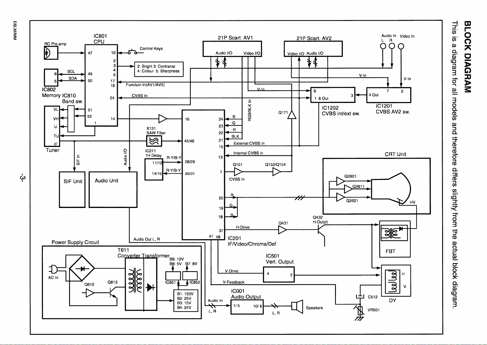
CIRCUIT DESCRIPTION
1. POWER SUPPLY
The power supply circuit of the
composed of a rectifier smoothing circuit, an oscillation
circuit, a control circuit and an output rectifier circuit. The
AC input voltage is full-wave rectified by the rectifier
smoothing circuit, and an unstable DC voltage is
generated at both terminals of the smoothing capacitor
C607.
This voltage is input to the oscillation circuit. The
oscillation circuit is provided with a blocking oscillator
circuit that switches the switching transistor Q613 ON
and OFF, and an oscillation frequency and a duty square
wave pulse are generated in the input windings
according to operation of the control circuit. A squarewave pulse whose size is dependent on the turn ratio of
the input and output windings is obtained in the output
winding. This is rectified in the output rectifier circuit, and
the desired DC voltage is obtained.
2. IF
&
DEFLECTION (TDA8361)
The IF output signal from the tuner passes through the
SAW filter, and it is input to pin45 and pin46 of
The signal input to the IC passes through the IF
amplifier, video detection and video amplifier circuits and
is output from pin7 as a composite video signal. And
after this signal is converted to impedance at Q151,
supplies to the video and chroma amplifier stages.
The sync.-separation circuit separates the video signals
applied to
video signal) to vertical- and horizontal-sync. signals
respectively. The horizontal oscillator requires no
external components and is fully integrated. The
oscillator is always running when the start-pin36 is
supplied with 8V. Horizontal drive signal is output from
pin37.
The separated vertical-sync. signal from sync. separation
circuit passes through the vertical-separation circuit, and
applied to trigger divider circuit. The horizontal oscillation
pulse and input vertical sync. pulse are monitored by the
trigger divider circuit, and switching 50Hz and 60Hz
system, the vertical amplitude automatically adjusted for
50Hz and 60Hz. The output signal from the trigger
divider is triggered vertical oscillation circuit consisting of
C351, R352 and pin42, and vertical drive pulse is output
from pin43.
feedback applied to pin41 and for adjustment of the
vertical amplitude.
3. VIDEO CHROMA
The composite video signal output from the pin7 of
IC101
pin13. The external video signal output from SCART is
supplied to pin15. The video signal input to pin13 or
pin15 is separated to luminance (Y) signal and chroma
signal in
H/V-sync. separation input. The peaking of Y signal is
adjusted by DC voltage of pin14. (“SHARPNESS”
pin1
3(internal video signal) or
VR361
is for adjustment of the horizontal centring.
VR501
is for changing the amount of AC
&
passes through
IC201.
These pins are used in common with
R.G.B. (TDA8361)
Q151-Q154,
EB4-A
and it is supplied to
chassis is
IC201.
pin1 5(external
control) The chroma signal is divided into R-Y and B-Y
chroma signals, demodulated in
pin30 (R-Y) and pin31 (B-Y). These chroma signals pass
through the
input to pin29 (R-Y) and pin28 (B-Y). These R-Y/B-Y
signals pass through RGB matrix circuit and RGB
selector circuit of ICI01 . The internal RGB signals are
generated in RGB matrix circuit and the RGB selector,
consisting linear amplifiers, clamps and selects either the
internal RGB signals or the external RGB signals input
from
pin22(R), pin23(G), pin24(B).
by the voltage at the RGB switch control (pin21) and
mixed RGB modes are possible since RGB switching is
fast. The RGB switch also functions as a fast blanking
pin by blanking the RGB output stages; here internal and
external RGB signals are overruled. The colour gain is
controlled by DC voltage of pin26. (“COLOUR” control)
The contrast control voltage present at pin25, and the
brightness control voltage present at pin17 controls DC
level of RGB signals. The RGB signals are finally
buffered before being available at the RGB output pins
[pin20 (R), pin19 (G), pin18 (R)].
4. AUDIO OUTPUT(TDA7263M)
The audio signals output from the audio unit are input to
pin1(L)
amplifier circuit and drive circuit, after which it is input to
the audio amplifier. The audio amplifier is an SEPP
(single-ended, push-pull) OTL type and output to
and
10(L)
5. VERTICAL OUTPUT
An IC (LA7832/LA7833) is used for the vertical output
circuit in this chassis. The vertical drive pulse from pin43
of
IC201
IC501,
of scanning a deflecting current is output from pin2 and
passes through the following path:
Vcc(B4) --)
VR501/R509.
In the last half of scanning the current path is C512
DY + pin2
an amplifying sawtooth waveform current flows directly to
DY to perform electron beam defection. Next, in the first
half of the banking period the vertical drive pulse
suddenly becomes OFF, and in order to reduce the
current flowing to DY, the current path becomes as
follows by the inductance of DY:
DY
+
pin2 +
when the charge of DY has dissipated, the current path
becomes Vcc24V
pin2 ->
prescribed current value is reached, the vertical drive
pulse becomes ON. This completes one cycle.
1H
delay line circuit
and 5(R) of IC171 and passes through the pre-
to directly drive the speakers.
(LA7832/LA7833)
is input to pin4 of IC501. This pulse drives
and vertical scanning is performed. In the first half
D501 + pin3 + pin2
An electric charge is then stored in C512.
--) pin1 + VR501/R509 +
pin1 + VR501/R509 +
+
pin6 + pin7 + C502 + pin3
DY + C512 +
VR501/R509,
IC201,
and output from
(IC271),
Selection is controlled
and they are
pin8(R)
--)
DY
--)
C512
C512. In this way,
C512 + DY. Also,
and when the
--)
+
+
-4-
E6LM/MM
Page 4

6. HORIZONTAL OUTPUT
A horizontal oscillation signal is output from pin37 of
IC201
and switches the drive transistor Q431. This
switching signal is current amplified by the drive
transformer T431 and drives the output transistor Q432.
When Q432 becomes ON, an amplifying current flows
directly to DY through C441
--)
DY
--)
0432 + GND,
and defection is performed in the last half of the
scanning period. Next, when Q432 becomes OFF, the
charge that had been stored in DY up to that point
releases a resonance current to the resonant capacitors
C421/C423 and charges them. The current stored in
C421/C423 is then flowed back to DY, and an opposite
charge is then stored in DY. This opposite charge then
switches the dumper diode in Q432 ON, the resonance
state is completed, and an amplifying current is then
flowed again directly to DY through the dumper diode.
By this means, deflection in the first half of the scanning
period is performed, and when Q432 becomes ON at
the end of the first half of the scanning period, deflection
during the last half is begun, thus completing one cycle.
In the PCC circuit consisting of Q461 and Q462, the
parabola signal supplied from the vertical circuit is
added at the horizontal output stage and pincushion
compensation is performed by varying the DC voltage
bias. Further, the ABL voltage is feedback to the base
of Q462 to compensate for width variations due to
variations in the beam current.
Pin25:
Black
Pin26:
IREF
Pin27: Odd/Even output
Pin28:
Pin29:
GND
-
Pin30: V-deflection stop output
Pin31:
RGB REF
Pin32: Blue output for OSD
Pin33: Green output for OSD
Pin34: Red output for OSD
Pin35: Blanking output for OSD
Pin36: H-sync. input (Horizontal pulse for OSD)
Pin37: V-sync. input (Vertical pulse for OSD)
Pin38-39: Supply
(+5V)
Pin 40: OSC GND
Pin 41: Oscillator input for CPU
Pin 42: Oscillator output for CPU
Pin 43: Reset input
Pin 44: Supply
(+5V)
Pin 45: Protect signal input (L:Power circuit defects)
Pin 46:
Ident.
signal input
Pin 47: R/C signal input
Pin 48: Mute output in no picture
Pin 49:
Pin 50:
Pin 51: Option SW5
IX
bus SCL (Serial clock)
1%
bus SDA (Serial date)
&
Band select output1
Pin 52: Band select output2
7. CPU
Pin
Pin1
Pin2:
Pin3:
Pin4:
<System
and Teletext Control>
description
: Tuning voltage output
Brightness control output (6-bit DAC)
Contrast control output
(6-bit
Colour control output (6-bit DAC)
DAC)
Pin5: Sharpness control output(6-bit DAC)
Pin6:
Not used (GND)
Pin7:
Not used (GND)
Pin8:
Pin9:
Pin10:
Pin1
Pin12: 50/60Hz switch input
Pin13:
Power ON/OFF output (H:ON)
AFT signal input
Option SW1 & Keyboard scan input (DC)
1: Option SW2
(50Hz:
Hi)
GND
Pin14: TV/AV switch output (TV: Hi)
Pinl5:
S-VHS switch output (S-VHS: Hi)
Pin16:
Option SW3 (2AV: Hi)
Pin17: Function signal input for SCART1
Pin18: Function signal input for SCART2
Pin19:
Power LED drive output1
Pin20:
Option SW4 & Power LED drive output2
Pin21
: Ignore output
Pin22:
GND
Pin23: CVBS input0 (Internal)
Pin24: CVBS input1 (Internal/External)
E6LM/MM
-5-
Page 5
Page 6

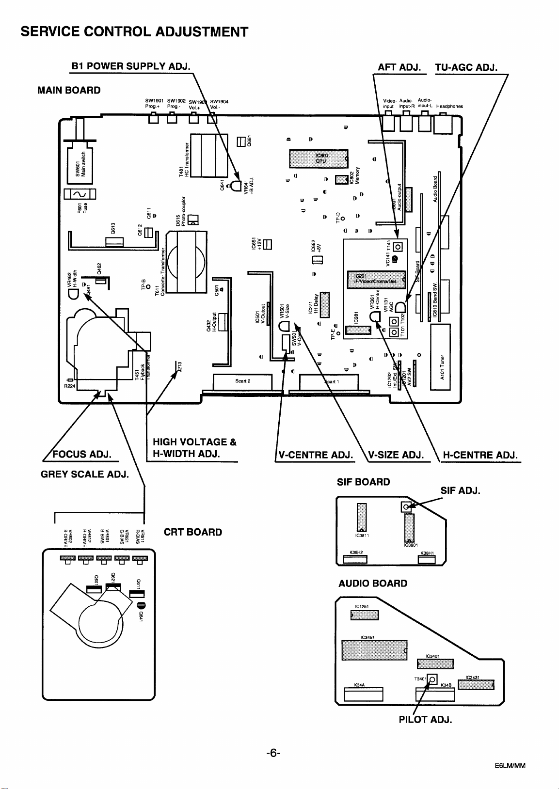
B1 POWER SUPPLY ADJUSTMENT
1. Set VR641 to it’s mechanical centre before pressing
the mains switch.
2. Tune the receiver to a PAL circular pattern.
3. Set the brightness and contrast controls to normal.
4. Connect a digital V-meter to test point “TP-B”.
5. By using VR641, adjust the voltage to 150
f
0.5 V.
AFT ADJUSTMENT
1. Tune the receiver to the clearest station.
2. By using
T141,
adjust AFT to obtain the best picture.
AGC ADJUSTMENT
NOTE: Do not attempt this adjustment with a weak
signal.
1. Tune the receiver to the clearest station.
2. Turn AGC VR(VR130) in direction which causes snow
noise to appear, then in the opposite direction until the
snow noise just disappears.
GREY SCALE ADJUSTMENT
HIGH VOLTAGE &WIDTH ADJUSTMENT
[HIGH VOLTAGE ADJUSTMENT]
1. Tune the receiver to circular pattern.
2. Set the brightness and contrast controls to maximum.
3. Connect digital V-meter to both terminals of R224, and
a high voltage meter to the CRT anode.
4. Confirm high voltage to be 26.0
f
1 KV at beam
current 1.3, and less than 29.0 KV at 0 beam current
(for 25 inch).
Confirm high voltage to be 26.0
f
1 KV at beam
current 1.4, and less than 29.0 KV at 0 beam current
(for 28 inch).
[H-WIDTH ADJUSTMENT]
Adjust VR462 to obtain proper H- width.
5.
6. Reconfirm high voltage.
H-CENTRE ADJUSTMENT
1. Tune the receiver to circular pattern.
2. Adjust H-centre by using VR361.
[SCREEN VR ADJUSTMENT]
1. Tune the receiver to the white pattern.
2. Set the brightness and contrast controls to normal.
3. Set VR2601and
VR2611
to its mechanical centre.
4. Turn VR2602, VR2612 and VR2622 fully anticlockwise.
5. Set the TV into service mode by pressing the
Function button
the Prog +
Function button
F(J
on the Remote control and
pAon
the TV front panel. Press the
F(J
on the Remote control until
“SCREEN” is highlighted. This sets up a
horizontal scanning line.
6. Set screen VR so that one colour is just visible.
[BIAS VR
ADJUSTMENT]
7. By using VR2602, VR2612 or VR2622, adjust line to
be white.
8. Set screen mode OFF, by pressing the Recall
(m
button
on the Remote control.
[DRIVE VR ADJUSTMENT]
Bv usina VR2601 and VR2611. adiust white balance.
9.
V-CENTRE ADJUSTMENT
1. Tune the receiver to circular pattern.
2. Adjust V-centre by using
SW501.
V-SIZE ADJUSTMENT
1. Tune the receiver to circular pattern.
2. Adjust V-size by using VR501.
FOCUS ADJUSTMENT
By using FOCUS VR, adjust focus control for good
scanning lines.
E6LM/MM
-7-
Page 7
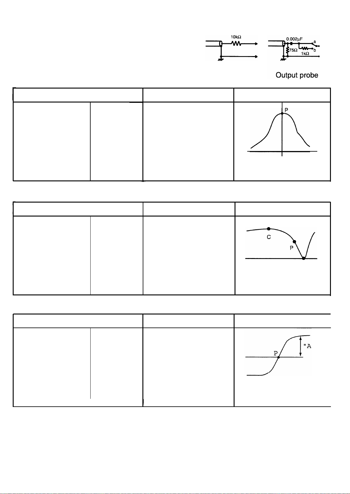
CIRCUIT ALIGNMENT
VIF alignment
DC
15.5V
AGC voltage
Output probe
Input probe
Marker frequency
Sweep
0dB=176mVrms/75
(4.3-4.5V)
ATT
Trap alignment
DC
15.5V
Output probe
Input probe
SETTING
SETTING
C644 +
IC201
-pin48
IC201
-pin45
(Side b)
IC201
-pin7
39.5MHz
20dB
C644 +
Tuner IF
(Side a)
Q101-C
Adjustment
By using T141, adjust
be maximum amplitude.
I
T
By using
be minimum amplitude.
Adjustment
T101,
adjust “A” to
Input probe
“P”
to
Waveform
Waveform
Marker frequency
Sweep ATT
0dB=176mVrms/75
SIF alignment
DC 12V
AGC voltage
Output probe
Input probe
Sweep
Marker Frequency
ATT
I
SETTING
41.5MHz
11dB
~
IC3801
-pin1 1
IC3801
IC3801 -pin1
(Side b)
IC3801 -pin1
1 OdB
38.5MHz
I
-pin3
I
A
Adjustment
1. Adjust AGC voltage to be
“A” =
0.5Vp-p.
2. By using T3801, adjust
to be equal centre line.
2
“P”
Waveform
-8-
E6LM/MM
Page 8
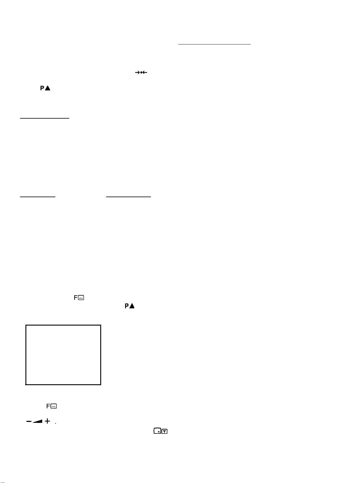
INITIALISATION (Important Notice)
When you replace a memory IC
necessary to initialise the IC as following step.
(IC802),
it is
A. Initialisation
Press and hold the normalisation button
remote control handset and press the programme +
button
The IC will be initialised automatically to set the
following data.
User control data
Colour
Brightness
Contrast
Sharpness
Text. Bright
Bass : Centre
Treble
Balance
Volume : Step 12
Service data
K1
K2
ST ID
A-l-T
pA
on the TV set.
: Centre
: Centre
: Maximum
: Centre
: Centre
: Centre
: Centre
: +000
: +000
: +000
:
+
Manual set data
->
->
004
+C
+001
-001
on the
Service mode description
K1,
K2 : For adjustment of stereo separation
ST ID
ATT
SCREEN: For screen adjustment
NOTE:
The items
adjustments for this model.
The data for
but has no effect.
: Mode setting for A2 stereo judgement
+000 : Fast mode
+001:
Normal mode
+002:
Fast -> normal mode
: Attenuation of FM sound
To equalise sound level between FM and
Nicam.
To make one horizontal scanning line.
K1,
K2, ST ID and
K1
,K2,ST ID and
ATT
are invalid
ATT
can be altered, but it
The initialised service data of items K1 and K2
should be modified to the manual set data shown
above.
For how to modify, refer to next step.
B. Service Mode
1. To entre the service mode, press and hold the
Function button
and press the programme + button
set.
The following OSD appears on the screen.
ADJUST DATA
K1
K2 +ooo
ST ID
ATT
SCREEN
CPU Ver
2. Select desired service item by using the Function
button
3. Change date by using the Level + or
--+.
4. To return to TV mode press the Recall button
on the remote control handset.
FT;;;1
FfJ
on the remote control handset
pA
on the TV
+ooo
+ooo
+004
VOL
1.0
on the remote control handset.
-
button
(m
E6LM/MM
-9-
Page 9
Page 10

Page 11

Page 12

Page 13

Page 14

Page 15

Page 16

Page 17

Page 18

Page 19

Page 20

Page 21

Page 22

Page 23

Page 24

Page 25

Page 26

Page 27

Page 28

Page 29

 Loading...