

Page 1

SERVICE MANUAL
MATSUI 14 V2R, 14 V2T
MATSUI
MATSUI 14 V2R, 14 V2T
Colour Television
Mastercare, Maylands Avenue, Hemel Hempstead, Hertfordshire, HP2 7JG, Telephone 01442 888000
Page 2
Es gelten die Vorschriften und Sicherheitshinweise
gemäß dem Service Manual "Sicherheit", Materialnummer 72010 800 0000, sowie zusätzlich die eventuell abweichenden, landesspezifischen Vorschriften!
The regulations and safety instructions shall be
valid as provided by the "Safety" Service Manual,
part number 72010 800 0000, as well as the
respective national deviations.
Inhaltsverzeichnis
Seite
Allgemeiner Teil ................................... 1-2…1-9
Typenschild des Gerätes (Version Number) ................................ 1-2
Modulübersicht............................................................................. 1-3
Technische Daten ........................................................................ 1-3
Sicherheits-Hinweise ................................................................... 1-4
Service Hinweise ......................................................................... 1-4
Schaltplansymbole ....................................................................... 1-5
Service und Sonderfunktionen..................................................... 1-9
Schaltungsbeschreibungen ............... 2-1... 2-6
1. Netzteil ..................................................................................... 2-1
2. Systemsteuerung ..................................................................... 2-2
3. TV-Signalprozessor TDA 8362 A ............................................. 2-3
Abgleich .........................................................3-1
Platinenabbildungen
und Schaltpläne ................................... 4-1…4-8
Chassisplatte ............................................................................... 4-1
Chassisplatte (vergrößert) ........................................................... 4-5
Oszillogramme Chassis ............................................................... 4-5
Gesamtschaltplan ........................................................................ 4-6
Bildrohrplatte 29305 022 8700..................................................... 4-7
Table of Contents
Page
General Section.................................. 1-2…1-10
Type Label on the set (Version Number) ..................................... 1-2
Module List................................................................................... 1-3
Technical Data ............................................................................. 1-3
Safety Advices ............................................................................. 1-4
Service Notes............................................................................... 1-4
Circuit Diagram Symbols ............................................................. 1-5
Service and Special Functions................................................... 1-10
Circuit Descriptions .......................... 2-7... 2-12
1. Power Supply ...........................................................................2-7
2. System Control ........................................................................2-8
3. TV Signal Processor TDA 8362 A ............................................2-9
Alignment.......................................................3-2
Layout of the PCBs
and Circuit Diagrams ........................... 4-1…4-8
Chassis Board.............................................................................. 4-1
Chassis Board (Enlarged)............................................................ 4-5
Oscillograms ................................................................................ 4-5
General Circuit Diagram .............................................................. 4-6
CRT Panel 29305 022 8700 ........................................................ 4-7
Ersatzteillisten.................................... 5-1…5-13
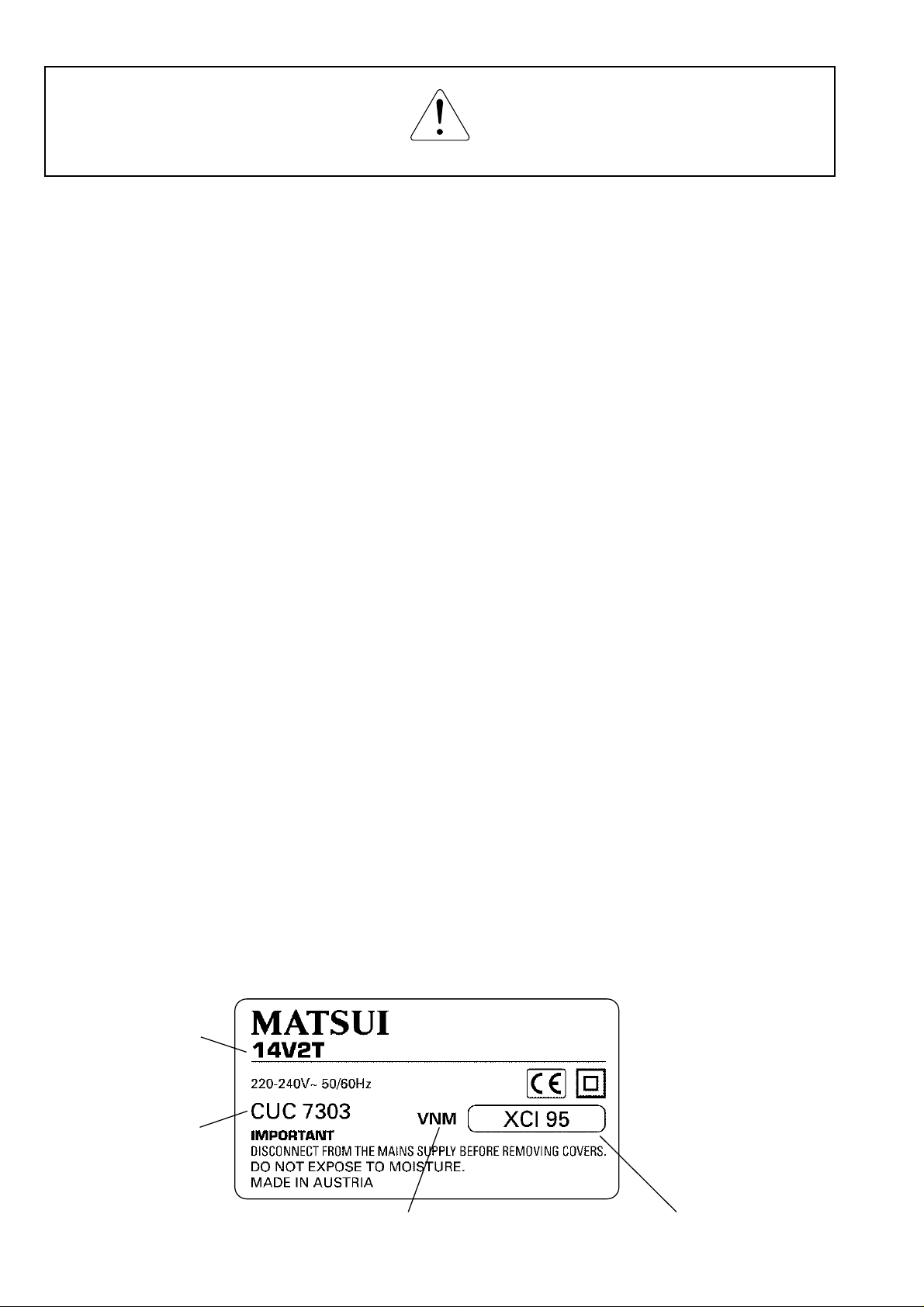
Typenschild des Gerätes
Zusätzlich zum Gerätetyp und der Chassisbezeichnung enthält das
Gerätetypenschild eine sogenannte "Version number" z.B. VNA. Diese Kennzeichnung gibt Aufschluss über den technischen/mechanischen Fertigungsstand.
Für die Bestellung von Ersatzteilen sind deshalb folgende Angaben
unbedingt erforderlich:
- Gerätetype (z.B. "14V2T")
- Chassis-Bezeichnung (z.B. "CUC 7303")
- Version number (z.B. "VNA")
- Materialnummer des Ersatzteils
Gerätetype
Type of product
Spare Parts Lists................................ 5-1…5-13
Type Label on the set
In addition to the type of the TV set and the designation of the chassis,
a so-called "Version number", e.g. VNA, is printed on the type label.
This identification gives information on the technical/mechanical state
of production.
Do not fail to give the following particulars when ordering spare parts:
– Type of product (e.g. "14V2T")
– Chassis designation (e.g. "CUC 7303")
– Version number (e.g. "VNA")
– Part number of spare part
1 - 2
Chassis-Bezeichnung
Chassis designation
Versionsnummer
Version number
Bestellnummer ohne Farbkennzeichnung
Order number without colour code
Page 3
Modulübersicht / Module List
Materialnummer
Part Number
Bestell-Nr.
Order No.
Chassis
Tuner
Bildrohrplatte
CRT Panel
tp Matsui 29642 062 0300
81406 016 1100
81406 016 1500
29305 022 8700
(CUC 7303 GB / VNM)
29704 004 1900
29704 004 2000
Technische Daten / Technical Data
14 V2R
(CUC 7303 GB / VNM)
Bildröhre / Picture Tube
Sichtbares Bild
Visible picture
Bildschirmdiagonale
Screen diagonale
Ablenkwinkel
Deflection angle
Bildwechselfrequenz
Vertical frequency
Elektronik / Electronic
Programmspeicherplätze
Programme positions
Kabeltuner
Cable tuner
TV-Normen
TV-Standards
Videotext
Teletext
Musikleistung
Music power
Anschlüsse Front / Connections Front
Kopfhörer
Headphones
Anschlüsse Rückwand / Connections Rear Panel
Mono 3,5mm Klinkenbuchse, schaltet eingebauten Lautsprecher ab
34cm 34cm
37cm (14")
tinted glass
90° 90°
50Hz 50Hz
69 TV + 1 AV 69 TV + 1 AV
nur / only UHF nur / only UHF
PAL, I PAL, I
–
2W 2W
Mono 3,5mm jack switch off inserted Loudspeaker
14 V2R
14 V2T
(CUC 7303 GB / VNM)
X.CI 9402 GB X.CI 9502 GB
29704 004 2300
29704 004 2400
••
••
••
14 V2T
(CUC 7303 GB / VNM)
37cm (14")
tinted glass
1-Seiten-Text
1-page-text
Euro AV 1 (schwarz/black)
Netzteil / Mains Stage
Netzspannung (Regelber.)
Mains voltage (variable)
Netzfrequenz
Mains frequency
Leistungsaufnahme
Power consumption
Standby ca. 9W ca. 9W
voll belegt
fully wired
165…265V 165…265V
50 / 60Hz 50 / 60Hz
ca. 38W ca. 38W
voll belegt
fully wired
1 - 3
Page 4

Sicherheits-Hinweise
Die in den Fernsehgeräten auftretende Röntgenstrahlung entspricht
den Bestimmungen der Physikalisch-Technischen Bundesanstalt
vom 8. Januar 1987.
Die Hochspannung für die Bildröhre und die damit auftretende
Röntgenstrahlung ist abhängig von der exakten Einstellung der
Netzteilspannung +A.
Nach jeder Reparatur im Netzteil oder in der Horizontalablenkung ist
die Hochspannung zu messen und ggf. einzustellen.
Schutzschaltungen im Gerät dürfen nur kurzzeitig außer Betrieb
gesetzt werden, um Folgeschäden am Chassis oder an der Bildröhre zu vermeiden.
Beim Austausch der Bildröhre dürfen nur die in den Ersatzteillisten
vorgeschriebenen Typen verwendet werden.
D
Servicehinweise
Chassisausbau
Bevor Sie die Chassis-Verbindungsleitungen lösen, muss die Leitungsverlegung zu den einzelnen Baugruppen wie Netzschalterplatte, Bedieneinheit, Bildrohrplatte, Ablenkeinheit oder Lautsprecher beachtet werden.
Nach erfolgter Reparatur ist es notwendig, die Leitungsführung wieder
in den werkseitigen Zustand zu versetzen um evtl. spätere Ausfälle
oder Störungen zu vermeiden.
Safety Advices
The X-radiation developing in the sets conforms to the X-radiation
Regulations (January 8, 1987), issued by the Physikalisch-Technische Bundesanstalt (federal physiotechnical institution).
The high tension for the picture tube and thus the developing Xradiation depends on the precise adjustment of the +A power
supply.
After every repair of the power supply unit or the horizontal deflection
stage it is imperative that the EHT for the picture tube is checked and
re-adjusted if necessary.
To avoid consequential damages to the chassis or the picture tube
the integrated protective circuits are allowed to be put out of
operation only for a short time.
When replacing the picture tube use only the types specified in the
spare parts lists.
Cable dereseau
Ces appareils ne peuvent être utilisés qu ' avec un cable de connecion
original de réseau avec bobine antiparasite intégré dans la fiche de
secteur. Ce câble de réseau empêche des perturbations de réseau et
est partie de l'autorisation d'appareil. Si nécessaire commandez
uniquement le cable de réseau selon la liste de pièces détachées.
Netzkabel
Diese Geräte dürfen nur mit dem Original-Netzanschlusskabel mit
integrierter Entstördrossel betrieben werden. Dieses Netzkabel verhindert Störungen aus dem Netz und ist Bestandteil der Gerätezulassung. Im Ersatzfall bestellen Sie bitte ausschließlich das Netzkabel laut Ersatzteilliste.
GB
Service Notes
Disassembly of the chassis
Before disconnecting the chassis connecting leads observe the way
they are routed to the individual assemblies like the mains switch
panel, keyboard control panel, picture tube panel, deflection unit or
loudspeaker.
On completion of the repairs the leads must be laid out as originally
fitted at the factory to avoid later failures or disturbances.
Mains cable
The TV receiver must only be operated with an original mains connecting
cable with an interference suppressor choke integrated in the mains
plug.This mains cable prevents interference from the mains supply and
is part of the product approval. For replacement please order exclusively
the mains connecting cable specified in the spare parts list.
F
Information pour la maintenance
Dèmontage de chassis
Avant de défaire les connecteurs du châssis princip, il y a lieu de
repérer auparavant les liaisons correspondant à chaque platine comme
par exemple le C.I. Inter secteur, le C.I. Commande, le C.I. Tube, le
bloc déviation ou les haut-parleurs.
A la fin de l'intervention, les connexions doivent être remises dans leur
position d'origine afin d'éviter par après d'éventuelles défaillances ou
perturbations.
I
Nota di servizio
Smontaggio del telaio
Prima di sfilare i cavi di collegamneto col telaio è necessario osservare
la disposizione originaria degli stessi verso le singole parti come la
piastra alimentazione, l'unità comandi, la piastra cinescopio, il giogo o
l'altoparlante.
Dopo la riparazione è necessario che gli ancoraggi e le guide
garantiscano la disposizione dei cavi analogamente a quella data in
fabrica e ciò per evitare disturbi o danni nel tempo.
Cavo rete
Gli apperechi devono essere messi in funzioni solo con il cavo originale
il colle gamento di rete e la sua spina di rete deve essere munita di una
bombina d´induttanza. In causa di sostituzione ordinate solo il cavo di
alimentatore che corrésponde alla lista degli accessori.
E
Nota de servicio
Desmontaje del chassis
Antes de desconectar las conecciones del Chassis hay que observar
la dirección de dichas conecciones a los distintos grupos de construcción
como la placa de conmutación de red, unidad de control, placa del
zócalo del tubo de imagen, unidad de deflección o altavoces.
Después de haber realizado la reparación y para evitar fallos o
pertubaciones posteriores es necesario reponer las conecciones tal
como fueron instaladas originalmente en fabrica.
Cable de red
El aparato solo se puede usar con el cable de red original con choque
antiparásito integrado en el enchufe de red. Este cable de red evita
perturbaciones de la red y es parte de la autorización del aparato. En
caso necesario puede pedir el cable de red según lista de piezas de
repuestos.
1 - 4
Page 5
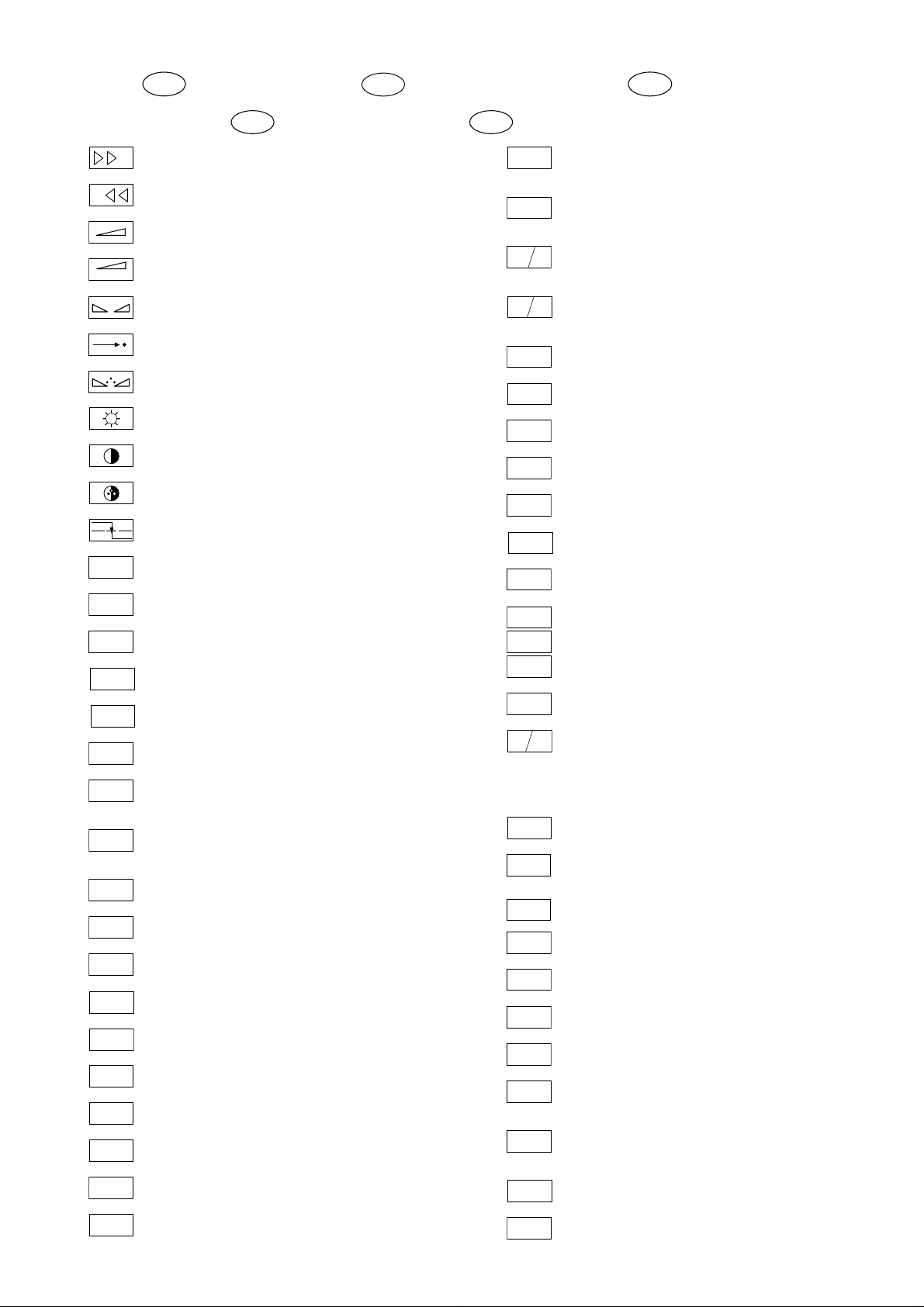
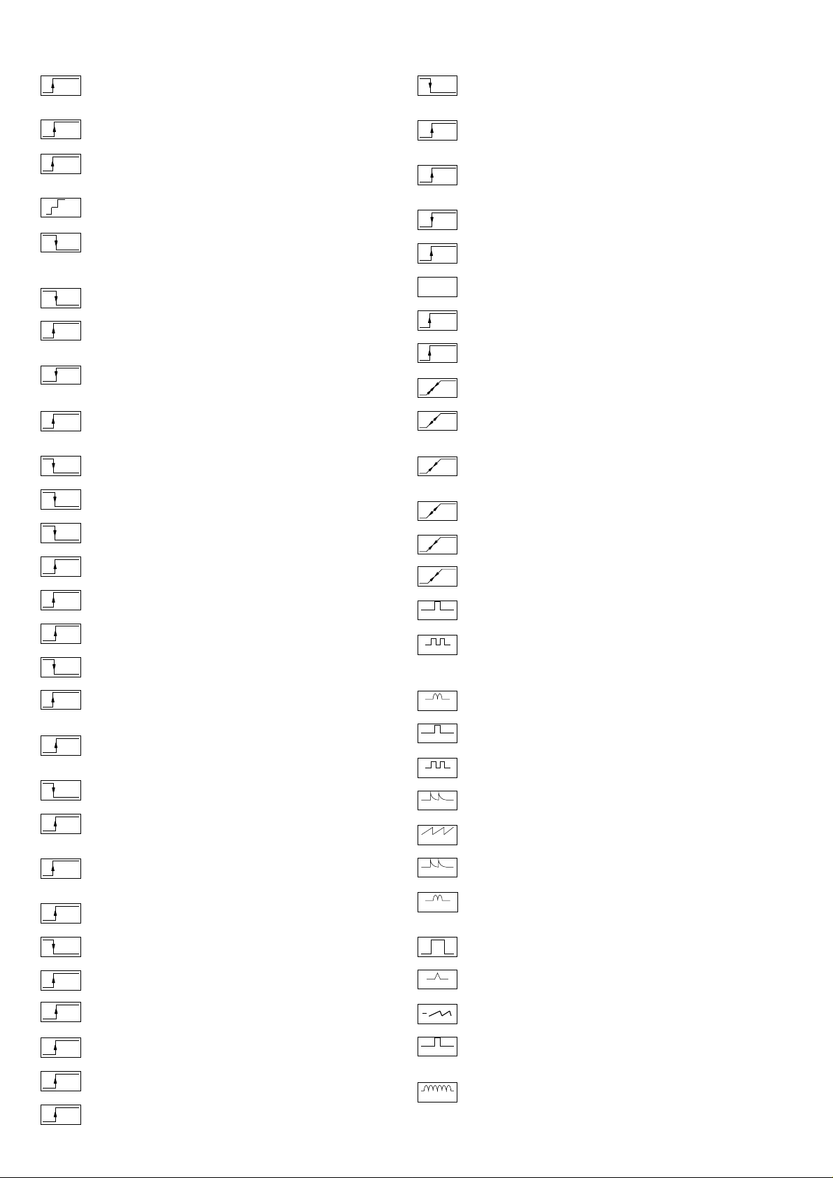
Schaltplansymbole
D
GB
Circuit Diagram Symbols
Symboles schéma
F
+
-
REF
A-AM
ABK
AUDIO
AUDIO-L
AUDIO-R
AUDIO
MAC
AUDIO
L-MAC
AUDIO
R-MAC
AUDIO
SUB
AUDIO
TV
AUDIO
VCR
A-ZF 1
A-ZF 2
B EXT
BB
B EXT
B
OSD
B PIP
Simboli sullo schema
I
Feinabst. + / Fine tuning + / Réglage fine + / Sint. fine + / Sint. fina +
Feinabst. - / Fine tuning - / Réglage fine - / Sint. fine - / Sint. fina -
Lautstärke / Volume / Volume / Volume sonore / Volumen
Referenz Lautstärke / Volume ref. volt. / Tens. de réf. vol. sonore /
Tens di rif. volume / Tens. ref. volumen
Balance / Balance / Balance / Balanciam. / Balance
Suchlauf / Self seek / Recherche autom. / Sint. autom. / Sintonia
automatica
Farbton / Tint / Teinte / Tinta / Tinte
Helligkeit / Brightness / Luminosité / Luminosita / Brillo
Kontrast / Contrast / Contraste / Contrasto / Contraste
Farbkontrast / Colour contrast / Contraste des coleurs / Contrasto
colore / Contraste de color
Schutzschaltung / Protection circuit / Circuit de sécurité / Circuito di
protezione / Circuito de protección
Audio AM
(Burst Key): Burstaustastimpuls / Burst blanking pulse / Impulsion de
suppress. de burst / Imp. di soppress. del burst / Imp. supresion burst
Ton-Signal / Audio signal / Signal audio / Segnale audio / Señal audio
Ton-Signal links / Audio signal left / Signal audio gauche / Segnale
audio sinistra / Señal audio izquierda
Ton-Signal rechts / Audio signal right / Signal audio droit / Segnale
audio destra / Señal audio derecha
Tonsignal D2 Mac / Audio signal D2MAC / Signal audio D2MAC /
Segnale audio D2MAC / Señal de sonido D2MAC /
Tonsignal links D2 Mac / Audio signal left D2MAC / Signal audio
gauche D2MAC / Segnale audio sinistro D2MAC / Señal de sonido
izquirdo D2MAC
Tonsignal rechts D2 MAC / Audio signal right D2MAC / Signal audio
droit D2MAC / Segnale audio destro D2MAC / Señal de sonido
derecho D2MAC /
Audio Tieftöner / Audio sub woofer / Audio haut-parleur pour les
frequences basses / Audio toni bassi / Audio sonido bajo
Audio-Signal FS Gerät / Audio signal TV set / Signal audio
téléviseur / Segnale audio TV / Señal audio TV
Tonsignal VCR Gerät / Audio signal VCR unit / Signal audio
magnetoscope / Segnale audio VCR / Señal audio VCR
Audio ZF 1 / Audio IF 1 / Audio FI 1 / Audio FI 1 / Audio FI 1
Audio ZF 2 / Audio IF 2 / Audio FI 2 / Audio FI 2 / Audio FI 2
Blau-Signal / Blue signal / Signal bleu / Segnale blu / Señal azul
Basisband / Baseband / Bande de base / Banda base / Banda base
Blau-Signal extern / Signal blue external /Signal bleu externe /
Segnale blu esterno / Señal azul externa
OSD-Einblendung blau / OSD blue / Eblouissement OSD bleu /
Visualizzazione OSD blu / Visualisacione OSD azul
Blau-Signal PIP / PIP Blue signal / Signal bleu PIP / Segnale blu
PIP / Señal azul PIP
Simbolos en los esquemas
E
Blau - Signal - 50Hz vert.,15625Hz hor. / Blue signal - 50Hz vert.,
B/50
15625Hz hor. / Signal bleu - 50Hz vert., 15625Hz hor. / Segnale bleu
- 50Hz vert., 15625Hz hor. / Señal azul - 50Hz vert., 15625Hz hor.
B/100
B-Y 50
B-Y 100
CENTER
CINCH
AUDIO L
CINCH
AUDIO R
CHROMA
CHROMA
Blau-Signal -100Hz vert., 31250Hz hor. / Blue signal -100Hz vert.,
31250Hz hor. / Signal bleu -100Hz vert., 31250Hz hor. / Segnale blu
-100Hz vert., 31250Hz hor. / Señal azul -100Hz vert., 31250Hz hor.
B-Y -Signal - 50Hz vert., 15625Hz hor. / B-Y -Signal - 50Hz vert.,
15625Hz hor. / Signal B-Y - 50Hz vert., 15625Hz hor. / Segnale BY - 50Hz vert., 15625Hz hor. / Señal B-Y - 50Hz vert., 15625Hz hor.
B-Y -Signal - 100Hz vert., 31250Hz hor. / B-Y -Signal - 100Hz vert.,
31250Hz hor. / Signal B-Y - 100Hz vert., 31250Hz hor. / Segnale BY - 100Hz vert., 31250Hz hor. / Señal B-Y - 100Hz vert., 31250Hz hor.
Kanalwahl / Channel selection / Sélection de canaux / Selez.
C
canale / Seleccion canal
Mittelpunkt-Lautsprecher / Center loudspeaker / Haut-parleur de
centre / Alto parlante punto centrale / Altavoz del centro
CHIP
Chip Adresse / Chip adress / Chip direction / Indiri. del chip /
ADR
Direccion chip
Ton-Signal Cinch links / Audio signal cinch left / Signal audio cinch
gauche / Segnale audio cinch sinistra / Señal audio cinch izquierda
Ton-Signal Cinch rechts / Audio signal cinch right / Signal audio
cinch droit / Segnale audio cinch destra / Señal audio cinch derecha
Chroma Signal / Chroma signal / Signal dégree / Croma segnale /
Señal croma
Chroma S-VHS-Signal / Chroma S-VHS-Signal / Signal dégree de
S-VHS
S-VHS / Croma segnale S-VHS / Señal croma S-VHS
Clock
CLK
CL 1
CL 2
Composite Sync. Imp. für VT / Composite sync pulse for TT / Imp. de
CSY
sync. vidéo-composite pour TXT / Imp. hor. para Video Comp.
CS 100
DATA
ENABLE
ENABLE
ENABLE
EURO-AV
AUDIO-L
EURO-AV
AUDIO-R
EURO-AV
VIDEO
Kombiniertes Hor./vert. Sync. Signal 31250Hz/100Hz (Composite
Sync.) / Combined hor./vert. sync signal 31250Hz/100Hz (Composite Sync) / Signal synchr. hor./vert. combiné 31250Hz/100Hz
(Synchr. composité) / Segnale sincr. orizz./vert. 31250Hz/100Hz
(Sincr. Composito) / Señal combinada sincr. hor./vert. 31250/100Hz
(Sincr. compuesto)
Daten / Data / Données / Dati / Datos
Verzögerungsleitung / Delay line / Ligne à retard / Linea di ritardo /
DL
Linea de retardo
Freigabe / Enable / Autorisation / Consenso / Habilitacion
ENA
ENA
Freigabe ZF / IF Enable / Validation FI / Consenso FI / Autorizacón FI
ZF
Freigabe FT / Finetuning enable / Autorisation Réglage fin / Abilitaz.
FT
Sintonia fine / Habilitacion Sintoinia fina
Freigabe LED / LED enable / Autorisation LED / Abilitaz. LED /
LED
Habilitacion LED
Freigabe Ton / Sound enable / Autorisation son / Abilitaz. audio /
TON
Habilitacion sonido
Audio-Signal EURO-AV links / Audio signal EURO-AV left / Signal
audio EURO-AV gauche / Segnale audio EURO-AV sinistra / Señal
audio izquierda EURO-AV
Audio-Signal EURO-AV rechts / Signal audio EURO-AV right /
Signal audio EURO-AV droit / Segnale audio EURO-AV destra /
Señal audio derecha EURO-AV
Video-Signal EURO-AV / Video signal EURO-AV / Signal video
EURO-AV / Segnale video EURO-AV / Señal video EURO-AV
Farb-Signal / Chroma signal / Signal chroma / Segnale chroma /
F
Señal croma
1 - 5
Page 6

FBAS
FBAS
CINCH
FBAS
MAC
FBAS
TON
FBAS
TXT
FBAS
TEXT
FBAS
SYNC.
FBAS
S-VHS
F
H
FRM
FT
F
U
F
V
G
G
OSD
G PIP
G EXT
G/50
G/100
GND - H
HA
HDR
HC
H
SYNC
HFB
HS
I2S CL
I2S TER
I2S IN
I2S WS
I BEAM
ICL
FBAS-Signal / CCVS signal / Signal vidéo composite / Segnale video
composito / señal video compuesta
FBAS-Signal-Cinch Buchse / CCVS signal-cinch socket / FBASprise à cinch / FBAS-presa cinch / FBAS-cinch
FBAS-D2 MAC / D2MAC CCVS signal / Signal vidéo compositeD2MAC / FBAS-D2MAC / FBAS-D2MAC
Basisband / Baseband / Bande de base / Banda base / Banda base
FBAS-Videotext / CCVS videotext / Signal vidéo compositeTélétexte / FBAS-Televideo / FBAS-Teletexto
FBAS Sync. Signal / CCVS sync signal / Signal sync. vidéo col.
comp. / Segnal sincr. video col. comp. / Señal sincr. video
compuesta
FBAS Signal S-VHS / CCVS signal S-VHS / Signal vidéo col. comp. SVHS / Segnal video col. comp. S-VHS / Señal video compuesta S-VHS
Hochspg. / EHT voltage / Haute tens. / Alta tens. / MAT
Rahmensignal / Frame signal / Signal d'encadrement / Segnale
cornice / Señal de marco
Feinabstimmung / Fine tuning / Reglage fin / Sint. fine / Sint. fina
FU-Signal / FU-signal / Signal FU / Segnale FU / Senal FU
FV-Signal / FV-signal / Signal FV / Segnale FV / Senal FV
Grün-Signal / Green signal / Signal green external / Signal vert /
Segnale verde / Señal verde
OSD-Einblendung grün / OSD green / Eblouissement OSD vert /
Visualizzazione OSD verde / Visualisacione OSD verde
Grün-Signal PIP / Green signal PIP / Signal green PIP/ Signal vert
PIP / Segnale verde PIP / Señal verde PIP
Grün-Signal extern / Green signal vertical / Signal vert externe /
Segnale verde esterno / Señal verde externa
Grün-Signal - 50Hz vert.,15625Hz hor. / Green signal - 50Hz vert.,
15625Hz hor. / Signal vert - 50Hz vert., 15625Hz hor. / Segnale
verde - 50Hz vert., 15625Hz hor. / Señal verde -50Hz vert., 15625Hz hor.
Grün-Signal -100Hz vert., 31250Hz hor. / Green signal -100Hz vert.,
31250Hz hor. / Signal vert -100Hz vert., 31250Hz hor. / Segnale
verde -100Hz vert., 31250Hz hor. / Señal verde -100Hz vert.,
31250Hz hor.
Nullpunkt Heizung / Ground filament / Point neutre-Chauffage /
Punto zero-Filamento / Punto medio filamento
Horiz. Sync. Impuls / Horiz. Sync pulse / Impulsion synchro. horiz. /
Impulso sincro orizzontale / Impulso de sinc. horiz.
Horiz. Ansteuerimpuls / Horiz. drive pulse / Impulsion de commande
horiz. / Impulso comando orizzontale / Impulso de control horiz.
Horiz. Klemmimpuls / Horiz. clamp pulse / Impulsion de serrage
horiz. / Impulso comando orizzontale / Impulso de garras horiz.
Horizontaler Sync-Impuls / Horizontal Sync impuls / Sync impuls
horizontale / Sinc impulso orrizontale / Impulso sync horizontal
Horiz. Rückschlagimpuls / Horiz. flyback / Impulsion de retour
horiz. / Impulso rotorno orizzontale / Impulso de retroceso horiz.
Hor. Sync. Implus für VT / Hor. sync pulse for TT / Imp. de sync. hor. pour
TXT / Imp. sincr. orizz. per Televideo / Imp. hor. para Video Comp.
Digitale Datensignale / Digtital data signals / Signal donneé digital /
Segnali dati digitali / Señal datos digital
Strahlstrom / Current beam / Current rayon / Corrante del irradire /
Corriente de haz
I2C Bus -Clock
IR
IM
CLOCK
IM
IDENT
IM
RESET
IR CLK
IR DATA
IR
VIDEO
KB
KH
AUDIO-L
KH
AUDIO-R
L
LED
M
MEGA
LOGIC
MODE
NIC CLK
NORM
OWA
P
P/C
PIP
P1
R
REMOTE
R
OSD
R PIP
R EXT
R-Y 50
R-Y 100
S
Infrarot-Signal / Signal infrared / Signal infra-rouge / Segnale
infrarosso / Señal infrarojo.
I2C Bus -Clock
I2C Bus -Kennung / I2C-Bus Identification / Identification I2C-Bus /
2
Ident. I
C-Bus, Identification I2C-Bus
I2C Bus -Reset
Infrarot Clock / Infrared clock / Signal I.R. horloge / Clock segnale
R.I. / Clock infrarojos
Infrarot Signal / Infrared signal / Signal I.R. / Segnale infrarosso /
Data infrarrojos
Infrarot Signal Video / Infrared signal video / Signal I.R. video /
Segnale infrarosso video / Data infrarrojos video
Keyboard
Tonsignal Kopfhörer links / Audio signal headphone left / Signal
audio gauche de casque / Segnale audio sinistra cuffia / Señal audio
izquierda auriculares
Tonsignal Kopfhörer rechts / Audio signal headphone right / Signal
audio droit de casque / Segnale audio sinistra cuffia / Señal audio
derecha auriculares
Lautstärke / Volume / Volume / Volume sonore / Volumen
Leuchtdiode / Light emitting diode / Diode lumineuse / Diodo
luminoso / Diodo luminescente
Speicher Taste / Memory button / Touche mémoire / Tasto di
memoria / Puls. memoria
Megalogic Daten / Megalogic data / Megalogic dates / Dati
Megalogic / Megalogic datas
Modus / Mode / Mode / Modo / Modo
NICAM Clock / Clock NICAM / Horloge NICAM / Clock NICAM /
Clock NICAM
Norm Taste / TV standard select button / touche de norme / Tasto
norma / Puls. de norma
Ost-West Ansteuerimpuls / East-west drive impuls / Impulsion de
commande Est-Ouest / Impulso comando Est-Ovest / Impulso de
control Este-Oeste
Programm / Program / Programme / Programma /Programa
Programm-Kanalwahl / Program channel selection / Progr. sélection
de canaux / Progr. selez.canale / Progr. selec. canal
Bild im Bild / Picture in picture / Image dans l'image / PIP / Imagen
en la imagen
Progr. Taste / Progr. button / Touche Progr. / Tasto Progr. / Puls.
Progr.
Rot-Signal / Red signal / Signal rouge / Segnale rosso / Señal rojo
Fernbedienung / Remote control / Telecommande / Telecomando /
Mando a distancia
OSD-Einblendung rot / OSD red / Eblouissement OSD rouge /
Visualizzazione OSD rosso / Visualisacione OSD rojo
Rot-Signal PIP / Red signal PIP / Signal rouge PIP / Segnale rosso
PIP / Señal rojo PIP
Rot-Signal extern / Signal red external / Signal rouge externe /
Segnale rosso esterno / Señal rojo externa
R-Y -Signal - 50Hz vert., 15625Hz hor. / R-Y -Signal - 50Hz vert.,
15625Hz hor. / Signal R-Y - 50Hz vert., 15625Hz hor. / Segnale RY - 50Hz vert., 15625Hz hor. / Señal R-Y - 50Hz vert., 15625Hz hor.
R-Y -Signal - 100Hz vert., 31250Hz hor. / R-Y -Signal - 100Hz vert.,
31250Hz hor. / Signal R-Y - 100Hz vert., 31250Hz hor. / Segnale
R-Y - 100Hz vert., 31250Hz hor. / Señal R-Y - 100Hz vert., 31250Hz hor.
Sonderkanal / Special channel / Canal special / Canale speciale /
Canal especial
1 - 6
Page 7

SB
SCL
SCL 100
SDA
SHIFT
VIDEO
SHIFT
TEXT
SS
SSB
SSC
SSC
PIP
SSC 100
SSC 50
SUR-
ROUND
SYNC
SYNC.
BTX
SYNC.
VT
SW
TE
T1
T2
TT
U
FOC
U
G1
U
H
U
G2
VA
VB
VCL
VDR
VG
Strahlstrombegrenzung / Beam current lim. / Lim. cour. de faisceau /
Lim. corr. di raggio / Corriente media de haz
I2C-Bus Clock
Schneller I2C-Bus Clock / I2C-Bus clock high speed / I2C-Bus grande
2
vitesse / I
I2C-Bus Daten / I2C-Bus data / I2C-Bus données / I2C-Bus dati /
2
I
Dynamische vert. Versch. 25Hz, aktiv bei Video u. Mix Betrieb /
Dynam. vert. shift 25Hz, active on video and mix operation / Decal
dynam. de l'image 25Hz, actif sur video et fonction. mixte / Spostam.
vert. dinam. 25Hz, attivo con video e. funzionam. misto / Desplaz.
dinamico vert. 25Hz, activo con video Y funciones mixtas
Dynamische vert. Versch. 25Hz, aktiv bei Standbild u. VT / Dyn. vert.
shift 25Hz, active on freeze-frame and Teletext / Decal dynam. de
l'image 25Hz, actif sur arret immage et Vidéotext (Antiope) / Spostam.
vert. dinam. 25Hz, attivo con fermo immag. e Televideo / Desplaz.
dinamico vert. 25Hz, activo con imagen parada Y Videotexto
Schutzschaltung / Protection circuit / Cablage protecteur / Pot. de
prot. / Circuito de proteccion
Spitzenstrahlstrombegrenzung / Peak beam current limiting / Lim.
de faisceau crete / Lim. corr. catod. di pico / Corrente pico de haz
Supersandcastle
Supersandcastle PIP
Supersandcastle 100Hz vert., 31250Hz hor.
Supersandcastle 50Hz vert., 15625Hz hor.
Surround
Sync.-Signal / Sync.-Signal / Signal sync / Segnale sync. / Señal de sync.
Sync. BTX / Viewdata Sync / Sync. Télétext / Sincr. Videotel / Sincr.
Videotexto
Sync. VT / Sync. Teletext / Sync Vidéotexte / Sincr. Televideo / Sincr.
Videotexto
Schwarzwert / Black level / Niveau du noir / Livello del nero / Nivel de negro
TEXT-Freigabe / TEXT enable / Autorisation TEXTE / Abilitaz.
TELEVIDEO / Habilatation TEXTE
Bei Zweiton, Ton 1 / On two channel sound, sound 1 / Pour double
son, son 1 / In bicanale, audio 1 / En dual, sonido 1
Bei Zweiton, Ton 2 / On two channel sound, sound 2 / Pour double
son, son 2 / In bicanale, audio 2 / En dual, sonido 2
Tieftöner / Woofer / Haut-parleur pour les frequences basses / Toni
bassi / Sonido bajo
Fokusspg. / Focussing volt. / Tens. de focalis. / Tens di focalizz. /
Tens focalizacion
Spg. Gitter G 1 / Volt. grid G1 / Tens grille G 1 / Tens. griglia G1 / Tens.
rejillas G 1
Hochspannung / High voltage / Haute tension / EAT / Alte tension
Schirmgitter Spg. / Screen-grid volt. / Tens. de grille - écran / Tens.di
griglia schermo / Tens. de rejilla
Vertikaler Ansteuerimpuls / Vert. drive pulse / Impulsion de commande
verticale / Impulso di comando verticale / Impulso de control vertical
VCR - Clock
Freigabe Anzeigebaustein / Display enable / Autorisation pour module
indicateur / Modulo indicazione / Habilitacion modulo indicacion
Vert. Gegenkopplung / Vert. feedback / Contre-reaction verticale /
Controreazione vert. / Aliment. neg. vert.
C-Bus veloce / Clock del I2C-Bus de alta velocida
C-Bus datos
VIDEO
VT DATA
VT SCL
VT SDA
V SYNC
Y
Y 50
Y 100
ZF
AFC
U
AV
U
B1
U
B2
U
U
BA
U
BTX
U
C-AV
U
DATA
DATA
U
EXT
DATA
U
OSD
U
DEEM
DS
U
EURO-
U
AV
EU-AV
U
CINCH
U
FBAS
U
HIFI
HIFI
U
MUTE
U
HUB
Video Signal / Video signal / Signal vidéo / Segnale video / Señal video
Videotext Daten / Teletext data / Données Teletexte / Linea dati
Televideo / Data Teletexto
Videotext Clock / Teletext clock / Signal horloge Vidéotext / Clock
Televideo / Clock Teletexto
I2C Bus: VT Daten / Teletext data / Données Vidéotext / Dati
Televideo / Data Teletexto
Vertikaler Sync-Impuls / Vertical Sync impuls / Sync impuls vertical /
Sinc impulso vertical / Impulso sync vertical
Y-Signal / Y Signal / Signal Y /Segnale Y / Señal Y
Y -Signal - 50Hz vert., 15625Hz hor. / Y -Signal - 50Hz vert., 15625Hz
hor. / Signal Y - 50Hz vert., 15625Hz hor. / Segnale
Y - 50Hz vert., 15625Hz hor. / Señal Y - 50Hz vert., 15625Hz hor.
Y - Signal - 100Hz vert., 31250Hz hor. / Y -Signal - 100Hz vert.,
31250Hz hor. / Signal Y - 100Hz vert., 31250Hz hor. / Segnale
Y - 100Hz vert., 31250Hz hor. / Señal Y - 100Hz vert., 31250Hz hor
Zwischenfrequenz / IF / FI / FI / FI
Schaltspg. AFC / AFC switching volt. / Tens. de commut. AFC/ Tens.
di commut. AFC / Tens. conmut. CAF
Schaltspg. AV / Switching volt. AV / Tens. de commut. AV / Tens. di
commut. AV / Tens. conmut. AV
Schaltspg. Band 1 / Switching volt. band 1 / Tens. de commut.
bande 1 / Tens. di commut. banda 1 / Tens. conmut. de banda 1
Schaltspg. Band 3/ / Switching volt. band 3 / Tens. de commut.
bande 3 / Tens. di commut. banda 3 / Tens. conmut. de banda 3
Schaltspg. Bildamplitude / Switching voltage vertical amplitude /
Tension de coupure amplitude dìmage / Tensione di commutaz.
ampiezza d'imagine / Tension de conm. amplitude de imagen di
commut. PAL / Tens. conmut. PAL
Schaltspg. BTX / Switching volt. BTX (Viewdata) / Tens. commut.
Télétext / Tens. commut. VIDEOTEL / Tens. conmut. Teletexto
Schaltspg. Camera Wiederg. über Camera-AV Eingang / Switching
volt. cam. playback via Camera-AV input / Tens de commut pour lec.
de camera par l'entree Camera-AV / Tens.de commut. in riproduz.
camera tramite ingresso Camera-AV / Tens. de serv. reprod. camera
a traves de la entrada Camera-AV
Schaltspg. Datenbetr. / Switching volt. data mode / Tens. de commut. fonct. données / Tens. di commut. dati / Tens conmut. datos
Schaltspg. U Data extern / Switching volt Data ext. / Tension de
commutation U Data externe / Tens. di commutazione U-Data
esterno / Tensión de conmutatón externa U
Schaltspg. für Bildschirm-Einblendung / Switching volt. for On
Screen Display / Tens. commut. pour eblouissement On Screen
Display / Tens. commut. per di visualizzazione On Screen Display /
Tens. conmut. para On Screen Display
Schaltspg. Deemphasis / Switching volt. deemphasis / Tens. commut. desaccent. / Tens. commut. deenfasi / Tens. conmut. deenfasis
Schaltspg. Dolby-Surround / Switching volt. Dolby-Surround / Tens.
commut. Dolby-Surround / Tens. commut. di Dolby-Surround / Tens.
de conmut. Dolby-Surround
Schaltspg. EURO-AV / Switching volt. EURO-AV / Tens. de commut.
EURO-AV / Tens. di commut. EURO-AV / Tens. conmut. EURO-AV
Schaltspg. EURO-AV-Cinch-Buchse / Switching volt. EURO-AVCinch socket / Tens. commut. prisa Scart - Cinch / Tens. commut.
presa Scart -Cinch / Tens. conm. EURO-AV - Cinch
Schaltspannung für Video-Ausgang EURO-AV Buchse / Switch.
voltage for video output EURO-AV socket / Tension de commut.
pour sortie vidéo EURO-AV / Tension commut. per presa d'uscita
video EURO-AV / Tension de conmut. para salida EURO-AV
Schaltspg. HIFI / Switching voltage HIFI / Tens. de commut. HIFI /
Tens di commut. HIFI / Tens. conmut. HIFI
Stummschaltung HiFi / Muting volt. HiFi / Commutation de silence
HiFi / Silenzametno HiFi / Muting HiFi
Schaltspg. HUB / Switching volt. deviation / Tens. commut.
1 - 7
Page 8
U
U
U
U
U
U
U
U
U
U
U
U
U
U
U
U
U
U
U
U
U
U
U
U
U
U
U
U
1 - 8
déviation / Tens. commut. deviazione / Tens. conmut. deviacion
IDENT
Schaltspg. Signalkennung AV 3 / Switching volt. signal identification
AV 3 / Tens de commut.identification de signal AV3 / Tens. commut.
identificazione segnale / Tens. conmut. identifi. segñal AV3
KH
Stummschaltung Kopfhörer / Muting volt. headphone / Commutation
MUTE
de silence casque / Silenzamento cuffia / Muting auriculares
KLEMM
Gleichspannung für SAT-Basissignal / DC for SAT basic signal /
Tens. continue pour SAT base signal / Tens continua per segnale
SAT base / Tens. continua para segñal SAT base
KOIN
Schaltspg. Koinz. / Switching volt. coinc. / Tens de commut. coinc. /
50/60Hz
Tens di commut. coinc. / Tens. conmut. coinc.
KOIN
Schaltspg. Koinz. mit Videoquelle verknüpft / Coinc. switching volt.
VQ
linked with video source / Signal de coincid. combiné avec source
video / Tens. di commut. a coinc. combinata con sorg video segñal
de coincidencia combinada con video
LED
Schaltspg. LED / Switching volt. LED / Tens de commut. LED / Tens.
commut. LED / Conmut. LED
Leucht-
Schaltspg. Leuchtpunktunterdrückung / Switching volt. beam spot
punkt
suppression / Tens. de commut. suppress. du spot lumineux / Tens.
soppr. punto luminoso / Tens. de conmut. filtro supresor del punto luz
LNC
Schaltspg. LNC "Aus" / Switching volt. LNC "OFF" / Tens. de
OFF
commut. LNC "OFF" / Tensione di commut. "Spento" LNC / Tension
LNC "OFF"
MAC
Schaltspg. D2MAC / Switching volt. D2MAC / Tension de
commutation D2MAC / Tens. di commutazione D2MAC / Tensión de
conmutación D2MAC
MUTE
Stummschaltung / Muting / Silencieux / Silenziamento /Muting
NF 1
Schaltspg. NF 1 / Switching volt. AF 1 / Tension commut. BF 1 / Tens.
commut BF 1 / Tens. conm. BF 1
NF 2
Schaltspg. NF 2 / Switching volt. AF 2 / Tension commut. BF 2 / Tens.
commut BF 2 / Tens. conm. BF 2
NIC
Schaltspg. NICAM / Switching volt. NICAM / Tens. de commut.
NICAM / Tens. commut. NICAM / Tens. de conmut. NICAM
NORM
Schaltspg. Norm / Switching volt. Norm / Tens. de commut.
standard / Tens. di commut. Norma / Tens. conmut. Norma
PAL
Schaltspg. PAL / Switching volt. PAL / Tens. de commut. PAL / Tens.
di commut. PAL / Tens conmut. PAL
POL.
Schaltspg. Polarität / Switching volt. polarity / Tension commut.
polarite / Tens. commut. polarita / Tens. conmut polarizacion
POWER
Schaltspg. Ökoschalter / Switching volt. eco switch / Tens. de
OFF
commut. interr. eco. / Tens. commut. interr. ecologico / Tens.
conmut. interr. ecol.
PV
Schaltspg. Panorama View / Switching volt. Panorama View / Tens.
de commut. Panorama View / Tens. commut. Panorama View /
Tens. conmut. Panorama View
RESET
Schaltspg. Reset / Switching volt. Reset / Tens. commut. Reset /
Tens. commut. Reset / Tens. conmut. Reset
RGB
Schaltspg. RGB1 - RGB2 / Switching volt. RGB1 - RGB2 / Tens. de
commut. RGB1 - RGB2 / Tens. di commut. RGB1 - RGB2 / Tens.
conmut. RGB1 - RGB2
SCHUTZ
Schaltspg.-Schutzfunktion / Switching volt.-protective func. / Tens
de commut.-sécurité / Tens. di commut.-funz di protez. / Tens.
conmut.-proteccion
SEC
Schaltspg. SECAM / Switching volt. SECAM / Tens. de commut.
SECAM / Tens. di commut. SECAM / Tens. conm. SECAM
STBY
Schaltspg. Standby / Switching volt. Standby / Tens. commut.
Veille / Tens. commut. Standby / Tens. conmut. Standby
S-VHS
Schaltspg. S-VHS / Switching volt. S-VHS / Tens.de commut.
S-VHS / Tens. de commut. S-VHS / Tens. de conmut. S-VHS
TON
Schaltspg. Ton 1-2 / Switching volt. sound 1-2 / Tens. commut. audio
1/2
1-2 / Tens. commut. son 1-2 / Tens. conmut. son 1-2
UHF
Schaltspg. UHF / UHF switching volt. / Tens. de commut. UHF / Tens
di commut. UHF / Tens. conmut. UHF
VHF
Schaltspg. VHF / VHF switching volt. / Tens. de commut. VHF / Tens
di commut. VHF / Tens. conmut. VHF
VQ
Schaltspg. Videoquelle / Switching volt. video source / Tens. de
commut. source video / Tens. di commut. sorg. video / Tens conmut.
U
WISCH
W/N
U
I / III
U
14V
U
22kHz
U
0/3/6/9V
4.5MHz
U
50/60
U
Hz
U
AFC
U
AFC
SAT
U
AGC
U
RE
U
TUN.
U
τ
HOR.
HOR.2FH
VERT.
VERT.
VER.2FV
VERT.
VERT.
VERT. 100
VERT. 100
REF.
PULSE
O/W
video
Schaltspg. Wischerkontakt / Schwitching voltage temp. contact /
Tens. de commut. contact fugitif / Tens. commut. contatto temporaneo / Contacto supresor tens. de conmut.
Schaltspg. ZF breit - schmal / IF switching volt. wide - narrow / Tens.
commut. FI large - etroit / Tens. commut. FI larga - stretta / Tens. FI
ancho - estrecho
Schaltspg. Bandwahl / Band sel. switching volt. / Tens. de commut.
select. bande / Tens. di commut. selez. banda / Tens. conmut. selec.
banda
14V Schaltspg. / 14V switching volt. / Tens. commut. 14V / Tens.
commut. 14V / Tens. de conm. 14V
22kHz Schaltspg. / 22kHz switching volt. / Tens. commut. 22kHz /
Tens. commut. 22kHz / Tens. de conm. 22kHz
0/3/6/9V Schaltspg. / 0/3/6/9V switching volt. / Tens. commut.
0/3/6/9V / Tens. commut. 0/3/6/9V / Tens. de conm. 0/3/6/9V
Schaltspg. 4,5MHz / Switching volt. 4.5MHz / Tens. de commut.
4,5MHz / Tens. di commut. 4,5MHz / Tens conmut. 4,5MHz
Schaltspg. 50-60Hz / Switching volt. 50-60Hz / tens. de commut.
50-60Hz / Tens. di commut. 50-60Hz / Tens. conmut. 50-60Hz
Regelspg. AFC / AFC contr. volt. / Tens. de regul. AFC / Tens. di
contr. AFC / Tens. regul. CAF
Regelspg. AFC Satellitentuner / AFC contr. volt. SAT tuner / Tens.
de regul. AFC tuner SAT / Tens. di contr. AFC Tuner SAT / Tens.
regul. CAF Tuner SAT
Feldstärkeabhängige Spg. / Fieldstrength-depent volt. / Contr. automatique de gain / Tens. dipent. intens. campo / Contr. autom. de gain
tens. CAG
Regelspg. / Contr. volt. / Tens. de regul. / Tens. di contr. / Tens regul.
Abstimmspg. Tuner / Tuning volt. tuner / Tens. d'accord tuner / Tens.
di sintonia tuner / Tens. sintonia tuner
Regelspg. Verzög. / Delayed contr. volt. / Tens. de regul. retardee /
Tens. regul. retardada
Horizontale Ansteuerung / Horiz. drive / Synchr. lignes / Pilotaggio
orizz. / Exitación horiz.
31250Hz Ansteuerimp. für Zeilenendstufe / 31250Hz Triggering
pulse for horiz. output / 31250Hz commande pour l'étage final
lignes / Imp. Pilotaggio di 31250Hz per stadio finale di riga / Impulso
de exitación 31250Hz para paso final de lineas
Vert. Parabel / Vert. parabolic signal / Signal parabolique vert. /
Segnale parab. vert. / Senal parabolica vert.
Vert. Tastimpuls / Vert. Gating pulse / Imp. trame / Imp. a cadenza
vert. / Imp. cuadro
Vert. Tastimpuls 100Hz / Vert. Gating pulse 100Hz / Imp. trame
100Hz / Imp. a cadenza vert. 100Hz / Imp. cuadro 100Hz
Vert. Sägezahn / Vert. saw tooth / Signal dent de scie / Dente di sega
vert. / Dientede sierra vert.
Vert. Tastimpuls / Vert. Gating pulse / Imp. trame / Imp. a cadenza
vert. / Imp. cuadro
Vert Sägezahn 100Hz / Vert saw tooth 100Hz / Signal dent de scie
100Hz / Dente di sega vert. 100Hz / Dientede sierra vert. 100Hz
Vert. Parabel 100Hz / Vert. parabolic 100Hz signal / Signal parabolique 100Hz vert. / Segnale parab. vert. 100Hz / Senal parabolica
vert. 100Hz
Tastimpuls / Gating pulse / Impuls de declenchement / Impulso a
cadenza / Imp. puerta
Ref. Impuls hor. / Reference impulse hor. / Imp. de refer.hor. / Imp.
di rifer. hor. / Imp. refer. horiz.
Klemmung Ein-Aus / Clamping On-Off / Clampage Marche-Arrêt /
Clamping Ins.-Disins. / Clamping Enc.-Apag.
Pulse für Polarotor / Pulses for Polar-Rotor / Impulsions Rotor de
Polariastion / Impulsi per Rotore Polarizzazione / Impulsos dara
Polarrotor
O-W Amplitude / E-W amplitude / Amplitude E-O / Ampiezza E-O /
Amplitud E-O
Page 9

Service- und Sonderfunktionen
1. Sonderfunktionen
1.1 Analogwertspeicherung
Eingestellte Analogwerte werden automatisch nach ca. 8 Sekunden
oder durch Schalten in den Standby-Betrieb gespeichert.
1.2 Optimalwerte einstellen,
Durch Tastendruck "AUX" –> "OK" werden die Optimalwerte für
Helligkeit, Kontrast, Farbstärke und Lautstärke eingestellt.
Optimalwert Maximalwert
Helligkeit 32 63
Farbkontrast 32 63
SW-Kontrast 50 63
Lautstärke 28 63
Nach Speicherung der Minimal-Lautstärke erscheint nach "Netz ein"
oder "Standby ein" der OSD Lautstärkebalken für ca. 8 Sekunden als
optischer Hinweis.
1.3 ATS Start
Taste "AUX" ca. 4s gedrückt halten bis die Einblendung "ATS" (Auto
Tuning System) erscheint, mit "OK" bestätigen.
Das ATS-System speichert das gefundene Sendersignal automatisch
(Anzeige: Kanal und Finetuning)
1.4 Versionsnummer (Prozessor)
Durch Drücken der Tasten "Ǻ" –> OK –> AUX wird die Versionsnummer des Prozessors eingeblendet.
1.5 Programmplatzwahl begrenzen (Umkehrpunkt):
Tasten "Ǻ" –> "OK" drücken. Es erscheint das Menü "Programmeinblen-
dung".
Mit den Tasten ǵ / Ƕ den Programmplatz anwählen der gesperrt
werden soll (z.B. 6).
Die Anzeige VHF1, VHF3 oder UHF mit der Taste Ƿ anwählen und mit
den Tasten ǵ / Ƕ auf "----" stellen.
Mit "OK" bestätigen und Menü mit "Ǻ" beenden.
Jetzt können nur die ersten 5 Programmplätze und AV mit den
Tasten ǵ / Ƕ angewählt werden.
Alle einstelligen Programmplätze -auch die gesperrten- können weiterhin mit den Tasten 0…9 angewählt werden.
Wird ab Programmplatz 11 gesperrt, sind alle Programmplätze mit den
Tasten 0…9 anwählbar.
1.6 Service-Menü aufrufen bei aktiviertem "Hotel mode on"
Fernbedientaste "Ǻ" gedrückt halten und Gerät mit der Netztaste
einschalten. Mit den Tasten ǵ / Ƕ über das Menü "Hotel" anwählen
und mit der Taste Ǹ / Ƿ Anzeige auf "OFF" stellen.
Bei aktiviertem "Hotel mode" ist der Aufruf des Programm-Menüs mit
der Taste "AUX" nicht mehr möglich.
2.5 Decoder
Über das Servicemenü Decoder "ON" oder "OFF" schalten.
Decoder "ON":
Automatische Erkennung der Schaltspannung an Pin 8 der EURO-AVBuchse (z.B. Descrambler-Betrieb bei Frankreichgeräten oder ext.
RGB-Betrieb für Italien).
2.6 Programmdauereinblendung
Zur Programmdauereinblendung die Taste "Ǻ" drücken. Nach ca. 8s
erscheint die Programmanzeige kleiner.
2.7 Remote C. (Remote Control)
1 - Remote Control ohne Farbtasten
2 - Remote Control mit Farbtasten
2.8 IDP2 HP
Händler-Programmer IDP2:
Sonderkanäle Frankreich "AUS": HP Mode auf "OFF" stellen.
Sonderkanäle Frankreich "EIN": HP Mode auf "ON" stellen.
2.9 TV ON
Netz EIN mit Programm 1 oder AV (Monitorbetrieb)
2.10 Blue Screen
Blauer Bildschirm ein / aus
3. Einstellungen über das AUX-Menü
3.1 AUX Übersicht
Kurzzeitiger Tastendruck der Fernbedientaste "AUX" ruft das AUX–
Menü auf.
3.2 Kontrastregelung aufrufen
AUX-Menü aufrufen und mit Taste " v - / v + " abstimmen.
3.3 Sleeptimer aufrufen
AUX-Menü aufrufen und mit der Taste "TXT" den Timer aktivieren. Mit
den Zifferntasten der Fernbedienung gewünschte Ausschaltzeit eingeben und mit Taste "Ǻ" Menü beenden.
3.4 Optimalwerte für Analogfunktionen
AUX-Menü aufrufen und Taste "OK" drücken. Die Optimalwerte sind
nun aufgerufen.
3.5 ATS
AUX-Menü aufrufen und Taste "AUX" ca. 4s gedrückt halten. Zum
Starten die Taste "OK" drücken.
2. Einstellungen über das Service-Menü
2.1 Service-Menü aufrufen
Fernbedientaste "Ǻ" gedrückt halten und Gerät mit der Netztaste
einschalten.
2.2 AGC Abgleich
Über das Servicemenü "AGC ALIGN" anwählen. Dieser Abgleich ist
mit den Tasten Ǹ / Ƿ zwischen den Werten 0…62 durchführbar.
2.3 OSD Position
Über das Servicemenü "OSD" (V bzw. H) anwählen und mit den
Tasten Ǹ / Ƿ die Menütafel in die Mitte des Bildschirms stellen.
2.4 Hotel Mode aktivieren
Über das Servicemenü "Hotel ON" anwählen.
Bei aktiviertem "Hotel mode"
- ist der Aufruf des Programm-Menüs mit der Taste "Ǻ" –> "OK" nicht
mehr möglich.
- wird die aktuelle eingestellte Lautstärke als maximale Lautstärke
gespeichert.
1 - 9
Page 10

Service and Special Functions
1. Special Functions
1.1 Storing the Analog Values
The entered analog values are either stored automatically after approx.
8 seconds or when switching to standby mode.
1.2 Setting the Optimum Values
Pressing "AUX" –> "OK" the television receiver is set to the optimum
values stored for brightness, contrast, colour contrast and volume.
Optimum Maximum
Brightness 32 63
Colour contrast 32 63
BW contrast 50 63
Volume 28 63
Having stored the minimum volume level, the volume setting bar is
indicated on the screen for approx. 8 seconds as an optical information
when switching the "power" on or switching on from "standby".
1.3 ATS Start
Press and hold the "AUX" button for approx. 4s until "ATS" (Auto
Tuning System) is indicated and confirm with "OK".
The ATS system stores the found station signal automatically (display:
channel and finetuning).
1.4 Version Number (Processor)
Pressing the "Ǻ" –> OK –> AUX buttons the version number of the
Processor is indicated.
1.5 Limiting channel position selection (reversing point):
Press the buttons "Ǻ" –> "OK". The menu "Channel display" appears.
With the buttons ǵ / Ƕ select the program position which is to be
limited (e.g. 6).
Select VHF1, VHF3 or UHF with button Ƿ and select the setting "----"
with buttons ǵ / Ƕ.
Save the setting with "OK" and end with "Ǻ".
Now only the first 5 channel positions and AV can be selected with
ǵ / Ƕ buttons.
All the single digit channel positions set including the "blocked" ones
can still be selected with the buttons 0…9.
If everything after channel position 11 is blocked, all channel positions
can be selected with the buttons 0…9.
1.6 Calling up the Service Menu at "Hotel mode on"
Press and hold button "Ǻ" on the remote control and switch on with the
mains button. With the ǵ / Ƕ button select the "Hotel" mode in the
menu and set the indication to "OFF" using the Ǹ / Ƿ button.
During the time the "Hotel mode" is active it is not possible to call up
the programme setting menu with the "AUX" button.
2.5 Decoder
Via the Service Menu switch the decoder "ON" or "OFF".
Decoder "ON":
Automatic identification of the switching voltage at Pin 8 of the EUROAV socket (e.g. descrambler operation with TVs in French version, or
external RGB mode for Italy).
2.6 Continuous Station Ident Indication
So that the programme name is displayed continuously on the screen
press the "Ǻ" button. After about 8 seconds the programme is displayed
in reduced size.
2.7 Remote C. (Remote Control)
1 - Remote Control without colour buttons
2 - Remote Control with colour buttons
2.8 IDP2 HP
Dealer Programmer IDP2:
France special channels „OFF“: set HP Mode to „OFF“.
France special channels „ON“: set HP Mode to „ON“.
2.9 TV ON
Mains power ON with channel position 1 or AV (monitor mode)
2.10 Blue Screen
Blue screen on / off
3. Settings via the AUX Menu
3.1 AUX Overview
The AUX menu is called up by pressing the "AUX" remote control
button quickly.
3.2 Calling up the Contrast Setting Option
Call up the AUX menu and adjust the contrast with " v - / v +" button.
3.3 Calling up the Sleeptimer
Call up the AUX menu and activate the timer with the "TXT" button.
Enter the desired stop time with the numbered buttons on the remote
control and leave the menu with button "Ǻ".
3.4 Optimum Values for Analog Functions
Call up the AUX menu and press "OK". The optimum values are now
called up.
3.5 ATS
Call up the AUX menu and press "AUX" for approximately 4s. Press the
"OK" button to start the system.
2. Settings via the Service Menu
2.1 Calling up the Service Menu
Press and hold button "Ǻ" on the remote control and switch on the set
with the mains button.
2.2 AGC Alignment
Select "AGC ALIGN" in the Service Menu. Alignment is possible in
range 0...62 with the Ǹ / Ƿ buttons.
2.3 OSD Position
Select "OSD" (V or H) in the Service Menu and with the Ǹ / Ƿ
buttons position the menu table in the centre of the screen.
2.4 Activating the Hotel Mode
Select "Hotel ON" in the Service Menu.
When the Hotel mode is activated
- it is no longer possible to call up the programme setting menu with
the "Ǻ" –> "OK" buttons.
- the currently set volume level is stored as the maximum level
possible in this mode.
1 - 10
Page 11
Schaltungsbeschreibung
1. Netzteil
1.1 Prinzipschaltung
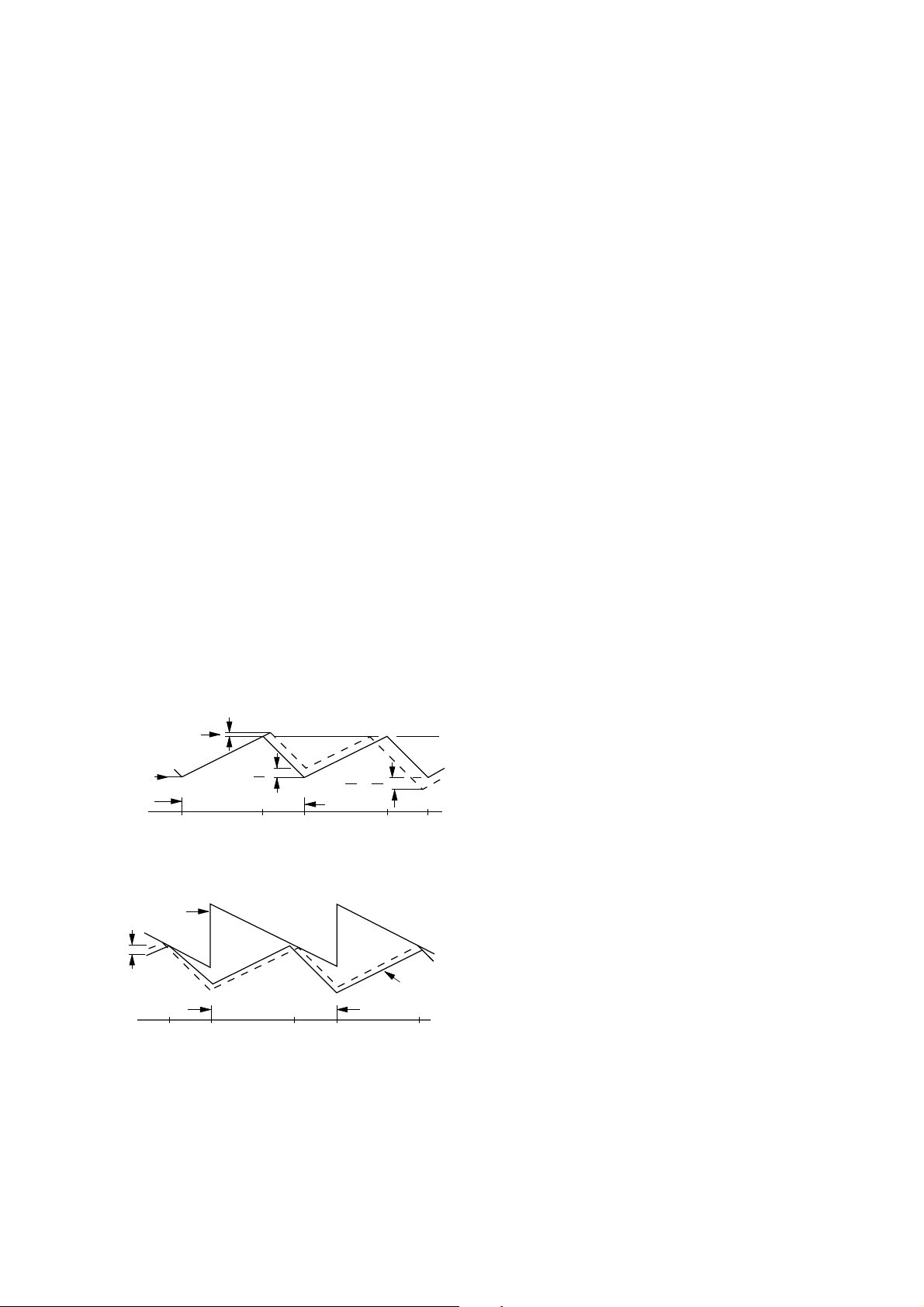
Sperrwandler können subharmonische Schwingungen aufweisen wenn
sie mit einem Arbeitstakt > 50% bei kontinuierlichem Induktionsstrom
betrieben werden. Diese Instabilität ist unabhängig von den Eigenschaften geschlossener Reglerkreise und wird durch die gleichzeitige
Messung der Festfrequenz und des Spitzenstroms verursacht.
In Fig. 1 ist diese Erscheinung graphisch dargestellt. An t0 beginnt der
Einschaltvorgang und damit steigt der Induktionsstrom mit einer
Steigung m1 an. Dieser Anstieg ist eine Funktion der Eingangsspannung im Verhältnis zur Induktanz. An t1 ist die maximale Stromstärke erreicht, die von der Steuerspannung festgelegt ist. Dadurch
wird die Sperrphase eingeleitet und der Strom fällt in einer Kurve m2 ab
bis zum nächsten Schwingungsvorgang. Die Instabilität lässt sich
zeigen, indem man ein Störsignal zur Steuerspannung addiert. Daraus
ergibt sich die kleine Stromänderung ∆I (gestrichelte Linie). Bei einer
festen Schwingungsdauer verkürzt sich die Sperrphase und die Mindeststromstärke in der Leitphase (t2) erhöht sich um ∆I + ∆I m2/m1. Die
Mindeststromstärke beim nächsten Zyklus (t3) fällt auf (∆l + ∆l m2/m1)
(m2/m1) ab. Diese Störgröße multipliziert sich mit m2/m1 bei jedem
folgenden Zyklus, so dass der Induktionsstrom beim Umschalten der
Polarität abwechselnd steigt und fällt. Bis der Induktionsstrom Null
erreicht, sind mehrere Schwingungszyklen notwendig. Anschließend
beginnt der Vorgang von neuem. Ist m2/m1 größer als 1, wird der
Sperrwandler instabil. Addiert man zur Steuerspannung eine künstliche Sägezahnspannung, die mit dem Pulsbreitenmodulations-Takt
synchronisiert wird, wie in Figur 1 dargestellt, verringert sich die
Störgröße ∆I in den nachfolgenden Zyklen und wird Null. Damit eine
Stabilität erzielt werden kann, muss die Steilheit dieser Korrekturspannung gleich oder etwas größer als m2/2 sein. Bei einer Korrekturspannung von m2/2 richtet sich der durchschnittliche Induktionsstrom
nach der Steuerspannung, so dass sich eine echte Stromregelung
ergibt. Die Korrekturspannung wird aus dem Oszillator abgeleitet und
entweder dem Spannungsrückkopplungs- oder dem Strommesseingang zugeführt (Fig. 2).
Fig. 1
∆l
Control Voltage
Inductor
Current
m1
t
0
∆l + ∆l
Oscillator Period
Fig. 2
Control Voltage
∆l
t
4
m1
Oscillator Period
1.2 Normalbetrieb / Regelbetrieb
Zur Stromversorgung des Gerätes wird ein Sperrwandlernetzteil mit
einer Schaltfrequenz von ca. 50kHz verwendet (bei Normalbetrieb und
einer Netzspannung von 230V).
Der Kollektoranschluss des Leistungstransistors T665 liegt über der
Primärwicklung 3/1 des Sperrwandlertrafos TR601 an der gleichgerichteten Netzspannung, D621…D624. Am Ladeelko C626 steht
bei 230V Netzspannung eine Spannung von ca. +320V.
m2
m
m
m3
(A)
2
1
t
1
∆l + ∆l
())(
t
2
m
m
2
2
m
m
1
1
t
3
(B)
m2
t
5
Inductor
Current
t
6
Die Ansteuerung sowie die Regel- und Überwachungsfunktionen des
bipolaren Leistungstransistors T665 übernimmt der IC630. Die Versorgungsspannung des Regel-ICs (Pin 7) liegt bei 12V. Nach dem
Erreichen der Einschaltschwelle an Pin 7 über den Widerstand R633
und den Kondensator C667 gibt der IC an Pin 6 einen positiven StartImpuls (1µs) von 10Vss ab. Nach dem Anlauf des ICs wird die
Versorgungsspannung über die Diode D667 aus der Wicklung 5/7 des
Wandlertrafos gewonnen. Während der Leitphase des Transistors
wird Energie im Übertrager gespeichert und in der Sperrphase über die
Sekundärwicklung abgegeben. Der IC630 regelt an Pin 6 über das
Tastverhältnis des Transistors T665 so nach, dass die Sekundärspannungen weitgehend unabhängig von Netzspannung, Netzfrequenz
und Last stabil bleiben.
Den Leistungstransistor T665 steuert ein Impulsbreitenmodulator an,
der von einem im IC integrierten Oszillator getaktet wird. Die Frequenz
bestimmen die Bauteile C652 und R652. Zur Stabilisierung vergleicht
der IC630 die über D654 gleichgerichtete Rückkopplungsspannung
mit der Referenzspannung von 5V an IC630-(8). Sinkt die Rückkopp-
lungsspannung durch größere Last geringfügig, wird der Ansteuerimpuls an Transistor T665 breiter. Dadurch verlängert sich die Leitzeit
von T665, so dass mehr Energie zur Kompensation der Last übertra-
gen wird. Am IC630-(3) liegt der Strom-Messeingang. Zieht die
Sekundärseite zu viel Strom, wird über den Strom-Messeingang Pin 3
die Ansteuerung IC630-(6) des T665 unterbrochen.
Bei einem Kurzschluss des Transistors T665 würde der Schaltkreis
UC3842 zerstört. Deshalb verhindern die Dioden D666 und D664,
dass die Spannung an Pin 3 die Spannung von 1,2V übersteigt. Die
Bauteile D668, C669 und R669 arbeiten als Snaperglied.
Durch die Bauteile CD654, C656, CD656 und CR656 wird ein verzö-
gertes Ansteigen der Startimpulse (Soft-Start) erreicht.
Mit dem Regler R654 werden die Sekundärspannungen über die
Kontrolle der Spannung +A bei Helligkeit- und Kontrast-Minimum
eingestellt.
1.3 Standby-Betrieb
Im Normalbetrieb steht am IC676-(1) (LM317) eine Spannung von ca.
10,5V. Soll das Gerät in Standby geschaltet werden, setzt der µP
U
auf "High" und damit IC676-(1) auf < 0,7V. Damit ist die
Standby
Spannung +B abgeschaltet und das Gerät schaltet in Bereitschaft.
1.4 Sekundärspannungen
+A: Stromversorgung für die Horizontalendstufe aus der
Wicklung 2/10 und D682. Auf diesen Wert wird das Netzteil eingestellt.
+33V: Die Abstimmoberspannung für den Tuner wird an der
Z-Diode D683 und dem Widerstand R681 aus der Wicklung 2/10 über D682 gewonnen.
+M =16,5V Stromversorgung für die Tonendstufe aus der Wicklung
6/10 und der Diode D671.
+B = 12V Stromversorgung für Tuner und horizontale Treiberstufe
T501. Diese Spannung kommt aus der Wicklung 6/10
über die Diode D671 und wird durch den Regler IC676
stabilisiert. Abschaltung der +12V siehe "Standby-Betrieb".
+E = 8V Stromversorgung für den Bildprozessor IC150, wird im
Standby-Betrieb abgeschaltet.
+H = 5V Stromversorgung für den µP IC850, Infrarotverstärker
IR810, den Tuner und CIC105.
Diese Spannung steht auch in Standby an.
Zusätzlich benötigte Spannungen
+D: +25V Stromversorgung für die Vertikalendstufe aus der Zeilen-
trafowicklung B/H über D444.
+C: 130V Die Stromversorgung für die Bildrohrplatte wird aus der
200V Zeilentrafowicklung G/H über R543 und die Diode D543
erzeugt: ca. 130V/14"-Bildröhre,
ca. 200V/17"…21"-Bildröhre.
2 - 1
Page 12
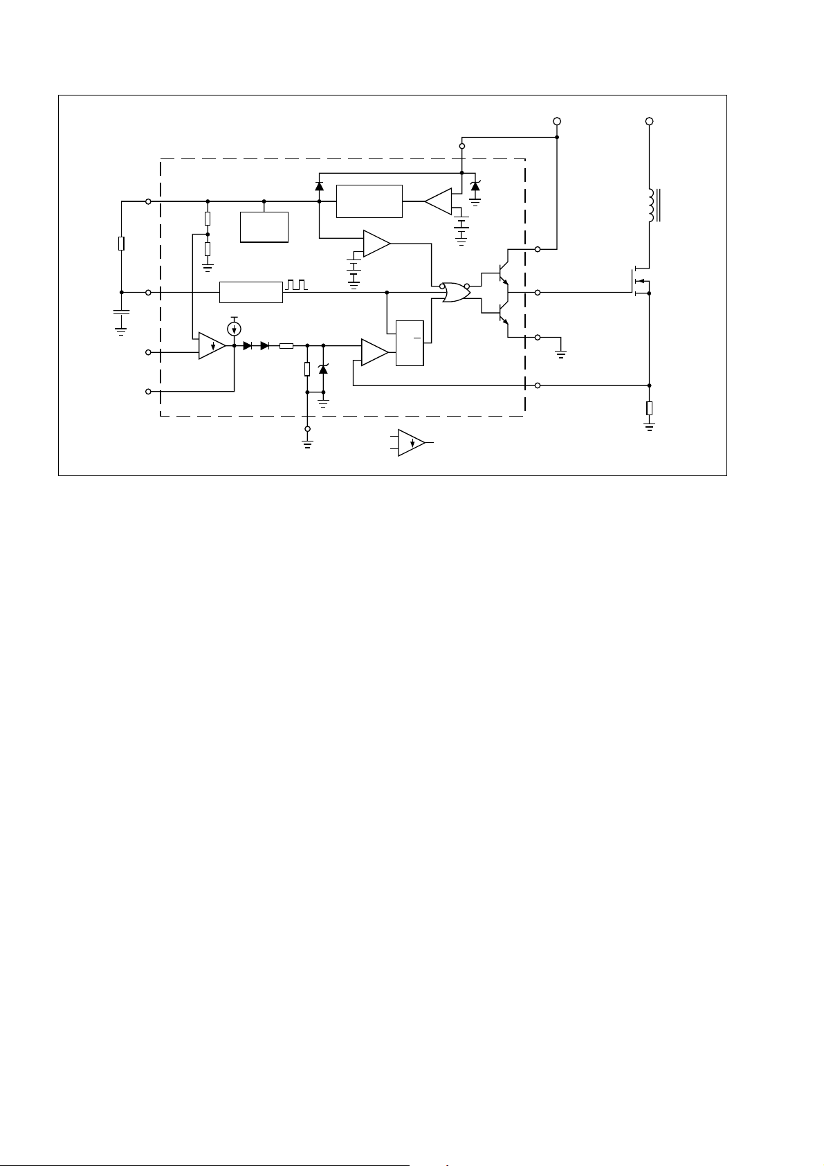
UC 3842A
R
T
C
T
Voltage Feedback
Input
Output
Compensation
V
cc
Vcc7
V
ref
8
2.5V
4
2
1
R
R
+
-
Error
Amplifier
Internal
Bias
Oscillator
1.0mA
2R
R
Gnd
Reference
Regulator
3.6V
1.0V
Current Sense
Comparator
5
+
-
UVLO
-
+
V
cc
UVLO
V
ref
S
Q
R
PWM
Latch
+
=
-
36V
Sink Only
Positive True Logic
V
c
7
Output
6
Power Ground
5
Current Sense Input
3
V
in
T665
R
s
2. Systemsteuerung
2.1 Mikrocomputer
Der maskenprogrammierte 8-Bit-Mikrocomputer IC850 (SDA5222 o.
Text) decodiert die eingegebenen Tastaturbefehle sowie die InfrarotFernbedienbefehle vom IR-Empfänger. Außerdem steuert er den
gesamten Systemablauf und die Bildschirm-Einblendung (OSD). Alle
Daten für die Programmplätze und Optionen werden in einem NVM
(nichtflüchtiger Speicher) gespeichert. Der Videotext ist im SDA5254
integriert.
Zur Funktion des Mikroprozessors sind folgende Grundbedingungen
notwendig:
- Betriebsspannung +5V/H an Pin 37
- Oszillatorfrequenz 18MHz an Pin 12, 13
- Reset-Impuls:
Nach jedem Einschalten mit der Netztaste wird der Prozessor an
Pin 15 über einen Reset-Impuls zurückgesetzt.
-I2C-Bus:
Der I2C-Bus ist ein bidirektionaler Zweileiterbus, bestehend aus der
SDA-Leitung (System-Daten) und der SCL-Leitung (System Clock).
Funktionskontrolle des Prozessors IC850:
Die I2C-Bus Leitungen liegen über die Pull-up-Widerstände CR869
und CR868 an +5V/H. Der Datenverkehr wird vom Prozessor, der den
Bustakt SCL erzeugt, gesteuert. Die Kontrolle der Daten- und ClockLeitung ist im Service nur über die Messung der TTL-Pegel (L ≤ 0,8V;
H ≥ 3,5V) möglich.
Servicehinweis:
Die I2C-Bus-Daten sind auch ohne Funktionsbefehl der IR-Fernbedienung vorhanden. Messen Sie auf der Datenleitung keine Busaktivitäten
liegt evtl. ein Schluss vor. Zur Lokalisierung des Fehlers werden dann
nacheinander alle am Datenbus angeschlossenen Bausteine oder
Bauteile abgelötet bzw. gezogen.
2.2 Initialisierung des Rechners nach dem Einschalten
Nach dem Einschalten baut sich die Spannung +5V/H auf, setzt den
IC850-(15) zurück und startet den Programmablauf.
Mit dem Startbefehl gibt der Prozessor an Pin 40 "High" aus und die
Spannung U
Spannungen +B, +12V (siehe Netzteil).
Nach dem Einschalten überträgt der Rechner (IC850) die Betriebsdaten aus dem internen Speicher über den I2C-Bus an die Bus-gesteuerten Bausteine und Schaltkreise.
startet das Gerät über CT826, IC676-(1) durch die
Standby
2.3 FBAS-Umschaltung EURO-AV-Buchse
Highpegel der Schaltspannung U
FBAS-Signal FBASSC an den Ausgang Pin 19 der EURO-AV-Buchse.
an IC850-(16) schaltet das
FBAS
2.4 Befehlseingabe
Das Keyboard liegt an der Dauerspannung +5V/H. Durch Auswertung
der unterschiedlichen Spannungspotentiale erkennt der Prozessor
IC850-(27), -(28) den eingegebenen Tastaturbefehl.
Die Fernbedienbefehle werden vom Infrarot-Empfänger IC810 verstärkt und an Pin 8 des µP decodiert.
2.5 Videotext IC850 (SDA5254)
Im IC850 (SDA5254) ist ein 1-Seiten Videotext integriert. Die Bildschirm-Einblendung ist in Zeilen und Spalten aufgeteilt. Zur Positionierung und Synchronisierung des Videotext-Bildes werden dem
IC850-(45), (46) horizontale und vertikale Vergleichsimpulse zugeführt. Die Aktivierung des Videotextes erfolgt intern über den I2C-Bus.
Der SDA5254 tastet über Pin 30 das FBAS-Signal nach Videotextdaten ab.
2.6 OSD-Einblendung
Bei einer OSD-Einblendung liefert die Schaltspannung "U
IC850-(50) "High" und schaltet IC 150-(21) ≤ 2V in den RGB-Modus.
Data
Der Zeichengenerator liefert die Einblenddaten über die Ausgangsports 47, 48, 49 des µP mit einer Amplitude von ca. 4,5V an die RGBEingänge IC150- (22), (23), (24) ca. 450mV.
2.7 Schutzschaltung U
An der Basis des Transistors T511 liegt über R511 der Fußpunkt der
Schutz
Vertikal-Endstufe und über R512, D512, D513 der Vergleichsimpuls F
aus der Horizontalendstufe. Im Fehlerfall schaltet die Basisspannung
ab 0,6V den Transistor durch und zieht über seinen Kollektor IC850-(32)
gegen Masse. Damit schaltet der µP das Gerät in Standby.
Bei Ausfall der Spannung +D fehlt am Ausgang der Vertikalendstufe
IC400-(5) die Gleichspannung und damit wird der Schutzschaltungseingang IC850-(32) nach Masse gezogen.
Gleichzeitig liegt der Kollektor (Leitung SB) über R513, D514, CD516
am Fußpunkt der Hochspannungswicklung. Bei zu hohem Strahlstrom
wird die Zenerspannung überschritten und zieht die Kollektorspannung
gegen 0V, damit schaltet das Gerät in Standby.
",
2 - 2
Page 13
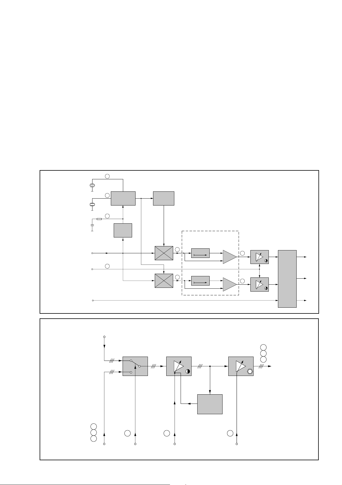
3. TV-Signalprozessor TDA8362A
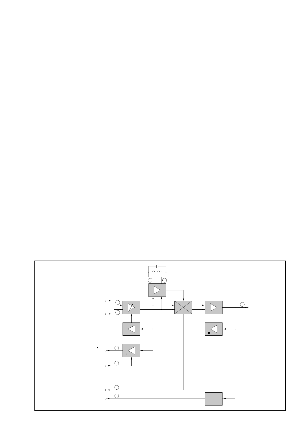
3.1 Übersicht
Bei diesem TV Konzept erfolgt fast die gesamte Verarbeitung des
Signals in einem einzigen IC, dem TV Signalprozessor TDA8362A.
In ihm sind integriert:
ZF-Signal:
- ZF-Verstärker
- Demodulator
- AFC
- AGC
- Koinzidenzkennung
FBAS Signal:
- Signalquellenumschaltung für das FBAS-Signal
- Luminanzverarbeitung
- Farbdemodulation
- Chrominanzverarbeitung
- Farbkontrastregelung
- RGB-Matrix
- C-AV-Eingang
- Signalquellenumschaltung für die RGB Signale
- Helligkeitsregelung
- Kontrastregelung
- Schwarzwertregelung (Cut-off)
Ton:
- Signalquellenumschaltung für den Ton
- Tondemodulation
- Lautstärkeregelung
Ablenkung:
- Amplitudensieb
- Zeilenoszillator
- ϕ1 Regelung
- ϕ2 Regelung
- Triggerimpulsgewinnung für die Zeilenendstufe
- Zeilenzähler
-Sägezahngewinnung für die Vertikalablenkung
- Treibersignal für die Vertikalendstufe
Zusätzlich kann der IC, je nach Beschaltung, Signale in PAL, NTSC
und SECAM Norm verarbeiten.
3.2 ZF
Die ZF kommt symmetrisch vom Tuner Pin 11 und 10 über das Filter
F901 und das Oberflächenfilter F906. Das vom Oberflächenwellenfil-
ter geformte Signal gelangt symmetrisch an die Pins 45 und 46 des
Signalprozessors. Die Demodulation des FBAS-Signals erfolgt in
einem Produktdemodulator. Der dafür benötigte Demodulatorkreis
F130 liegt an Pin 2 und Pin 3. Das demodulierte Signal durchläuft
einen Verstärker und steht an Pin 7 des ICs (BB). Der IC erkennt intern
das Synchronsignal ohne Auftastung durch den Zeilenrückschlag-
impuls. In Abhängigkeit des Synchronpegels wird eine Regelspannung
erzeugt. Diese Regelspannung wirkt zunächst auf den geregelten
Eingangsverstärker der ZF. Über den Pin 49 wird eine Referenzschwelle URV eingestellt. Unterhalb dieser Schwelle wird nur der
Eingangsverstärker der ZF geregelt. Bei Überschreitung dieser Schwelle wird von Pin 47 die Regelspannung Ut an den Tuner gelegt. Pin 47
ist ein Open-Kollektor- Ausgang. Die Spannung beträgt im ungeregelten Fall etwa 5V. Erhöht sich die Eingangsamplitude, so verringert
sich der AGC Pegel. Im Demodulator wird die Gleichspannung für die
AFC gewonnen. Pin 9 gibt dieses Signal als Stromausgang aus.
Steigt die empfangene Frequenz, so sinkt die Regelspannung für die
AFC. Der Prozessor IC850 wertet dieses Signal aus und zieht den
Tuner über Finetuning nach. Aus dem demodulierten Signal wird vom
Sync Detektor geprüft, ob Synchronsignale vorhanden sind. Ist dies
nicht der Fall, geht IC150-(4) auf "Low". Damit erkennt der Prozessor
IC850-(33) die fehlende Koinzidenz und schaltet den Ton stumm.
3.3 FBAS Signal
Das demodulierte FBAS-Signal verläßt den IC150-(7), TDA8362A als
Basisband noch gemeinsam mit der Ton ZF. Das FBAS-Signal wird im
weiteren Verlauf vom Tonsignal befreit. Nach dem Transistor CT921
und dem Ton-Trap F923 und F924 wird das Signal aufgeteilt.
Über Transistor CT110 und IC2807 (Option) steht es als FBAS
Videotext-Decoder IC850-(30) und über die Transistoren CT963,
am
SC
CT962 an der EURO-AV-Buchse Pin 19.
Als FBAS steht es am Signalquellenumschalter IC150-(13).
Der zweite Eingang des Signalquellenumschalters Pin 15 ist mit der
EURO-AV-Buchse Pin 20 verbunden.
Der Prozessor IC850-(42), Spannung UVQ, Transistor CT840 trifft an
IC150-(16) die Auswahl, ob das Signal vom Tuner oder von extern
verarbeitet werden soll.
3.4 Externes FBAS-Signal
Am Signalquellenumschalter IC150-(15) steht entweder ein externes
FBAS-Signal von der EURO-AV-Buchse oder das HF-FBAS-Signal.
Die Spannung UVQ an IC150-(16) wählt aus, ob das FBAS-Signal der
EURO-AV-Buchse, oder das HF-FBAS-Signal weitergeleitet werden
soll. IC150-(16) "Low" internes -, IC150-(16) "High" externes Signal.
Achtung: Ist die "Decoder Ein" Kennung gesetzt, erwartet das Gerät
ein Signal von der EURO-AV-Buchse. Das FBAS-Signal vom Tuner
ist aber am Ausgang Pin 19 der EURO-AV-Buchse messbar.
Bild-ZF und Demodulation
Vision IF and Demodulation
vom Prozessor
from Processor
Coincidence
ZF vom Tuner
IF from Tuner
U
~
für denTuner
for the Tuner
URV
AFC
Koinzidenz
F130
2 3
45
46
47
~
49
9
4
TDA8362A
Detector
Sync
FBAS- und Ton-
7
Ausgang
CCVS and Sound
Output
2 - 3
Page 14
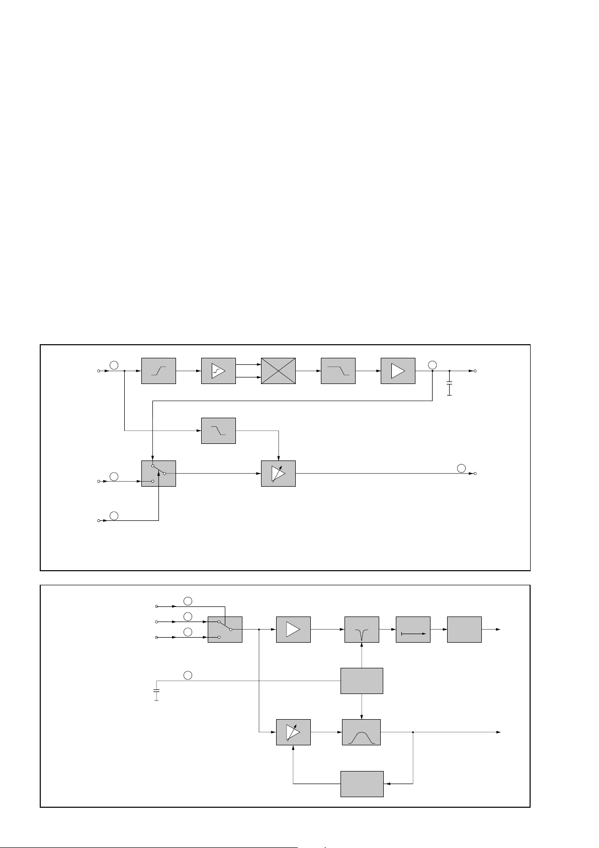
3.5 Ton-ZF
Dem Tonsignal ist nach dem Keramikfilter F926 an IC150-(5) eine
Gleichspannung zur Einstellung der Lautstärke unterlegt. Die
Demodulation erfolgt in einem PLL Demodulator.
Einmal wird das demodulierte und ungeregelte NF Signal an IC150-(1)
ausgekoppelt, von den Transistoren CT917, CT916 verstärkt und zur
EURO-AV-Buchse geleitet.
Zum anderen steht das demodulierte und geregelte NF-Signal an
IC150-(50) und gelangt zum NF-IC TDA7233.
3.6 Luminanz- und Chrominanz-Signal
Die Kalibrierung und Regelung erfolgt automatisch während der
Bildaustastlücke. Eine Änderung der Einstellung resultiert aus einem
positiven oder negativen Strom in den Integrationskondensator CC177
an IC150-(12). Während des sichtbaren Teils wird die Regelung
geklemmt.
Das Luminanzsignal durchläuft den im IC integrierten Farb-Trap. Eine
im IC eingebaute Verzögerungsleitung kompensiert die Laufzeitunterschiede zwischen Luminanz- und Chrominanzsignal. Die anschließende Verbesserung der Kantenschärfe (Peaking) wird ebenfalls im
IC realisiert. Dabei werden die ansteigenden und abfallenden Flanken
des Y-Signals versteilert. Im internen Farbfilter wird das Chrominanzsignal aus dem FBAS-Signal herausgefiltert. In einem Regelkreis wird
die Amplitude des Farbsignals für den Farblimiter und die Farbregelung
kontrolliert und gelangt als Chromasignal auf den Farbdemodulator.
Aus dem Chromasignal wird der Burst herausgelöst, der den
Farboszillator in Frequenz und Phase synchronisiert. Der Quarz legt
die Frequenz von 4,43MHz für den Farbhilfsträger an Pin 35 fest. Ein
interner PLL-Kreis regelt ihn. Die Nachregelspannung wird über die
Zeitkonstante an Pin 33 integriert. Mit Hilfe des Farbträgers werden
nun die Farbkomponentensignale demoduliert und verlassen als R-Y
(Pin 30) und B-Y (Pin 31) den IC150. Nach der PAL-Verzögerung
durch den CIC105 TDA4665 werden die beiden Signale B-Y und R-Y
wieder in den IC150-(28), -(29) TDA8362 A eingespeist und geklemmt.
Anschließend erfolgt die Regelung des Farbkontrastes an IC150-(26).
In der Matrix werden aus den verstärkten Signalen mit Hilfe des
Y-Anteils die RGB-Signale erzeugt.
3.7 SECAM-Signalweg und automatische PAL-SECAM-Umschaltung
Das Chromasignal von ca. 300mV steht für den SECAM-IC110 an
IC150-(27).
Im SECAM-Betrieb steht an IC110-(16) eine Spannung von 5,6…5,8V
Hat der IC110 über das Chromasignal an Pin 16 SECAM erkannt, wird
an Pin 1 eine Stromquelle aktiviert, die an IC150-(32) SECAMIdentifikation meldet. Erkennt IC150 ebenfalls SECAM, schaltet er den
Pin 32 auf 5V (bei PAL 1,5V). Dieser Gleichspannung wird bei PAL
eine gleichmäßige Taktfrequenz und bei SECAM Impulspakete mit
einer Frequenz von 4,43MHz überlagert.
Der IC110 nimmt dies als Bestätigung an und schaltet die DifferenzSignalausgänge R-Y und B-Y (Pin 9 und 10) auf 3,5V DC (bei
PAL 1,5V). Die Differenzsignalausgänge des IC150-(30), -(31) werden dadurch gesperrt. IC110 liefert jetzt R-Y und B-Y. Über die
Laufzeitleitung CIC105 gelangen die Differenzsignale zurück zum
IC150. Der weitere Verlauf der Signale ist unter 3.6 "Luminanz und
Chrominanz Signal" beschrieben.
Bei SECAM-Empfang wird der DC-Pegel 3,5V an IC110-(10). Über
CT115 wird U
ATS-Suchlauf PAL oder SECAM-Empfang erkennen (nur Frankreich).
Bei OIRT-Empfang (6,5MHz Tonträger) schaltet CT915 über U
und CT115 den Suchlaufmodus des µP (U
"Low" (PAL="High") und der µP IC850-(1) kann bei
PAL
) um.
PAL
AUDIO
Ton-ZF +
Lautstärkeregelung
Sound IF +
Volume Control
Ton von Scart
Sound from Scart
Schaltsignal vom
Prozessor
Switching Signal
from Processor
5
6
16
Ton-ZF und Demodulation
Sound IF and Demodulation
Schaltsignal vom Prozessor
Switching Signal from Processor
FBAS von HF
CCVS form RF
FBAS von Extern
External CCVS
HPF
PLL
1
Demodulator
LPF
16
13
15
LPF
Farb-Trap
Colour Trap
Deemphasis
Delay
50
Peaking
2dB
Ungeregelter
Ton Scart
Uncontrolled
Sound to Scart
Geregelter Ton
Controlled Sound
Y
Regelspannung für
die Calibrierung
Control Voltage
for Calibration
Filterung des Luminanz- und Chrominanzsignals
Luminance and Chrominance Filter
2 - 4
12
Autom.
Calibrierung
Auto Calibration
Farb-Filter
Chroma Filter
Farb-Limiter
Farb-Regler
Chroma Limiter
Chroma Control
CH
Page 15
3.8 RGB-Signalweg
Für die Kontrasteinstellung der RGB-Signale erzeugt der IC850-(23)
eine variable Regelspannung für den Kontrastverstärker an IC150-(25).
Da bei zu großem Strahlstrom die Bildröhre beschädigt werden
könnte, begrenzt die Schaltung den Strahlstrom. Die interne
Spitzenstrahlstrombegrenzung erfolgt in der Spitzenweiß-Begren-
zung. Überschreitet das RGB-Signal 2,3Vss, setzt die interne Spitzenweiß-Begrenzung ein und regelt den Kontrast zurück, die externe
Spitzenstrahlstrom-Begrenzung setzt bei ca. 2Vss ein.
Bei der mittleren Strahlstrombegrenzung wird die Einstellspannung an
IC150-(25) für Kontrast verringert.
Nach dem Helligkeitsverstärker verlassen die RGB-Signale den IC150
und gelangen zu den Kathodenverstärkern auf der Bildrohrsockelplatte.
3.9 Gewinnung der H- und V-Synchronsignale
Am TV-Signalprozessor IC150-(13), -(15) ist das FBAS-Signal von der
ZF und der EURO-AV-Buchse angeschlossen. Nachdem ein interner
Farbtrap die Farbinformationen aus dem FBAS-Signal herausgefiltert
hat, wird das Y-Signal zur weiteren Signalverarbeitung und für das
Amplitudensieb aufgeteilt.
Das Amplitudensieb erzeugt den Horizontal- und Vertikalsynchronimpuls aus dem Y-Signal. Das Horizontal-Synchronsignal gelangt nun
auf die ϕ1-Regelung, das Vertikal-Synchronsignal startet den Zeilenzähler für die Vertikalsynchronisation.
3.10 Zeilenoszillator
Bei diesem IC-Konzept generiert der Zeilenoszillator die Zeilenfrequenz
vollständig intern. Er besitzt keine externen Bauteile. Somit sind weder
die freilaufende Horizontal- noch die freilaufende Vertikalfrequenz
einzustellen.
3.11 ϕ1-Regelung
Die ϕ1-Regelung stellt eine Frequenzregelung dar. Damit wird der
Horizontal-Oszillator auf die Frequenz des Zeilensynchronsignals
geregelt. Hierzu wird die Frequenz des Zeilensynchronsignals mit der
Frequenz des Horizontal-Oszillators verglichen.
Ein ϕ1-Regelkreis definiert die Zeitkonstante der Regelspannung, die
an IC150-(40) ausgegeben wird. Die Regelspannung verschiebt den
Zeilenoszillator solange, bis die Frequenzen übereinstimmen.
3.12 ϕ2-Regelung
Die ϕ2-Regelung ist die Phasenregelung. Sie stellt den Phasenbezug
zwischen dem Zeilensynchronsignal und der tatsächlichen Position
des Elektronenstrahls her. Schaltungs- und strahlstrombedingt bestehen unterschiedliche Verzögerungszeiten zwischen dem Außen-,
dem Triggersignal und der tatsächlichen Reaktion der Zeilenendstufe.
Diese Unterschiede werden durch die ϕ2-Regelung ausgeglichen.
Für die Strahlposition ist der Zeilenrückschlagimpuls vom Zeilentrafo
am IC150-(38) angeschlossen. Die ϕ2-Regelung erzeugt aus dem
Oszillatorsignal und dem Zeilenrückschlagimpuls eine Regelspannung
am IC150-(39), die mit CC166 gesiebt wird.
Chroma-Signal
Farbkontrast vom
Prozessor
Colour Contrast
from Processor
Luminanzsignal
Luminance Signal
34
3,58
MHz
35
Farb-Oszillator
Colour Oscillator
4,43
4,43
MHz
MHz
33
26
RGB intern
Internal RGB
Burst
PLL
H/2
PAL-Schalter
PAL Switch
(R-Y)
(B-Y)
Farbdemodulation
Colour Demodulation
TDA4662
TDA4665 (OIRT/FR)
30
31
Delay
Delay
29
+
28
+
(R-Y)
(B-Y)
RGB
Matrix
R
G
BY
RGB-Ausgangsverstärker
RGB Output Amplifier
RGB von Scart
oder Videotext
RGB from Scart
or Videotext
22
23
24
RGB extern
External RGB
21 25
Data Kontrast
Contrast
Spitzenweiß
Begrenzung
Peak White
Limiting
17
Helligkeit
Brightness
20
19
18
RGB zur
Bildrohrplatte
RGB to the
CRT panel
2 - 5
Page 16

3.13 Supersandcastle SSC
Das 3-pegelige Supersandcastlesignal IC150-(38) ist ein KombiImpuls bestehend aus dem Horizontal-, Vertikal- und Burstauftastimpuls. Der Zeilenrückschlagimpuls (H-Sync) wird über T523,
CR163 dem IC150 zugeführt. Die Bildrückschlag- und Burstkeyimpulse
werden im IC generiert.
Bei Ausfall der Vertikalablenkung zieht IC400-(7) den SSC-Pegel über
R401 auf "Low" und steuert an IC150-(18), -(19), -(20) RGB den
Bildschirm dunkel. Dabei werden die Analogwerte auf "Low" gezogen.
3.14 Cut-Off-Einstellung
Die statischen Arbeitspunkte der Bildröhre werden über die Cut-OffAutomatik stabil gehalten. Dazu gibt der IC150 in der Zeile 23, 24 und
25 einen Impuls an die R, G, B-Kathoden aus um den Strahlstrom
jedes Systems zu messen (ca. 10µA). Der Cut-Off-Strom während der
Messzeilen wird über Widerstand CR156 dem IC150-(14) zugeführt.
Der IC vergleicht diesen Strom mit einem internen Referenzwert und
bildet daraus den Arbeitspunkt für den Schwarzwert der Videoendstufen
bzw. die Cut-Off-Spannung der Bildröhre.
3.15 HDR-Endstufe
Nach interner Verstärkung steht an Pin 37 das Horizontale Ansteuersignal für den Zeilenendstufentransistor.
3.16 Vertikal-Ablenkung
Der Vertikal-Generator wird in diesem IC-Konzept durch einen Zeilenzähler ersetzt.
Werden keine Synchronimpulse empfangen, so läuft der Zeilenoszillator unsynchronisiert. Aus dem Zeilenoszillator leiten wir den
"Vertikaloszillator" ab. Es muss nur die Anzahl der Zeilen gezählt
werden. Nachdem der Zähler 312 Zeilen festgestellt hat, wird ein
Bildsynchronsignal ausgegeben. Damit ist sowohl die horizontale als
auch die vertikale Ablenkung ohne externe Synchronisation sichergestellt.
Wird ein Synchronsignal empfangen, dann läuft zunächst der Zeilenoszillator synchron. Der Zeilenzähler liefert auch hier ein vertikales
Ablenksignal. Kommt nun ein Vertikalsynchronsignal, wird der
Sägezahngenerator nicht mehr vom Zeilenzähler sondern direkt vom
Vertikalsynchronsignal getriggert.
Der Sägezahngenerator besteht aus einer Konstantstromquelle, die
einen externen Kondensator auf- und wieder entlädt. Die Ladezeit gibt
das Vertikalsynchronsignal vor. Am Kondensator C158, IC150-(43) ist
der Vertikal-Ablenksägezahn messbar.
Um die Bildhöhe in der Vertikalendstufe IC400 einstellen zu können,
muss der Ablenksägezahn beeinflusst werden. Die Veränderung des
Ablenksägezahns muss noch vor der Vertikalendstufe durchgeführt
werden. Dazu steht an IC150-(42) von dem IC400 ein FeedbackSignal zur Gegenkopplung. Wie bei einem Operationsverstärker auf
dem Minuseingang lassen sich dadurch die gewünschten Parameter
einstellen.
3.17 Non-Interlace Kompensation bei Videotext (25Hz Modulation)
Wird ein Videotext-Signal dargestellt, springt das Videotext-Signal
ständig um eine Zeile rauf und runter (Videotext-Signal im NonInterlace). Um dieses Springen zu verhindern, sendet der VideotextIC850-(52) ein 25Hz Schaltsignal an IC150-(43). Aus dieser Schaltspannung U
lenksägezahn abgeleitet. Damit verschiebt sich das erste Halbbild
wird ein kleiner Gleichspannungs-Offset für den Ab-
25Hz
nach oben. Die geraden und die ungeraden Zeilen werden nun jeweils
übereinandergeschrieben.
3.18 Koinzidenz
Die Koinzidenz-Information wird im ZF-Teil gewonnen und am IC150-(4)
ausgegeben.
Regelzeitkonstante
für die
ϕ
1-Regelung
Control Time Constant
for
ϕ
1-Control
ϕ
H-Sync
FBAS
CCVS
Amplitudensieb
Sync Separator
V-Sync
H/V-Synchronisation und Ablenkung
H/V Synchronisation and Deflection
Enable Oszillator
Enable Oscillator
40 36
1
Zeilenoszillator
Line Oscillator
Zeilenzähler
Line Counter
SB VFB
Flyback
38 39
ϕ
2
43 42
25 Hz
Regelzeitkonstante für die
ϕ
2-Regelung
Control Time Constant
for
ϕ
2-Control
+
-
37
HDR
44
VDR
2 - 6
Page 17

Circuit Description
1. Power Supply
1.1 Basic Circuit
Current mode converters can exhibit subharmonic oscillations when
operating at a duty cycle greater than 50% with continuous inductor
current. This instability is independent of the regulators closed loop
characteristics and is caused by the simultaneous operating conditions of fixed frequency and peak current detecting.
Figure 1 shows the phenomenon graphically. At t0, switch conduction
begins, causing the inductor current to rise at a slope of m1.This slope
is a function of the input voltage divided by the inductance. At t1, the
Current Sense Input reaches the threshold established by the control
voltage. This causes the switch to turn off and the current to decay at
a slope of m2, until the next oscillator cycle. The unstable condition can
be shown if a pertubation is added to the control voltage, resulting in
a small ∆l (dashed line). With a fixed oscillator period, the current decay
time is reduced, and the minimum current at switch turn-on (t2) is
increased by ∆l + ∆l m2/m1. The minimum current at the next cycle (t3)
decreases to (∆l + ∆l m2/m1) (m2/m1). This pertubation is multiplied by
m2/m1 on each succeeding cycle, alternately increasing and decreasing the inductor current at switch turn-on. Several oscillator cycles may
be required before the inductor current reaches zero causing the
process to commence again. If m2/m1 is greater than 1, the converter
will be unstable. Figure 1 shows that by adding an artificial ramp that
is synchronized with the PWM clock to the control voltage, the ∆l
pertubation will decrease to zero on succeeding cycles. This compensating ramp (m3) must have a slope equal to or slightly greater than
m2/2 for stability. With m2/2 slope compensation, the average inductor
current follows the control voltage yielding true current mode operation. The compensating ramp can be derived from the oscillator and
added to either the Voltage Feedback or Current Sense inputs (Figure 2).
Fig. 1
The IC630 is responsible for driving, controlling and monitoring the
bipolar power transistor T665. The supply for the control-IC is 12V and
is present on Pin 7. As soon as the switch-on threshold is reached on
Pin 7 via the resistor R633 and the capacitor C667, the IC feeds out a
positive start pulse (1µs) of 10Vpp at Pin 6. After start-up of the IC, the
supply voltage is obtained via the diode D667 from the winding 5/7 of
the transformer. During the conducting phase of the transistor, energy
is stored in the transformer and this is transferred into the secondary
winding when the transistor is switched off. The IC630 controls by the
period during which the transistor T665 is switched on, the transfer of
energy at Pin 6 so that the secondary voltages are stable and are
largely not affected by variations of the mains supply, mains frequency
and the load.
The power transistor T665 is driven by a pulse-width modulator which
is triggered by an oscillator integrated in the IC. The frequency of the
oscillator is determined by the components C652 and R652. For
stabilisation, the feedback voltage which is rectified by D654 is
compared in IC630 with the 5V reference voltage provided at IC630-(8).
If the feedback voltage decreases by a small amount due to a heavier
load the drive pulse to the transistor T665 is prolonged. As a result, the
conducting period of T665 will be longer so that additional energy
transfer will be provided to compensate for the load. Pin 3 of IC630 is
a current sense input and will stop the drive to T665 at IC630-(6) in the
event of excessive current drain from a heavy secondary load.
If there was a short circuit condition at the transistor T665, the circuit
UC3842 would be destroyed. Therefore, the diodes D666 and D664
are provided to avoid the voltage at pin 3 exceeding 1.2V. The
components D668, C669, and R669 work as a snap stage.
The components CD654, C656, CD656, and CR656 delay the rise of
the pulse start duration (soft start).
The adjustment control R654 is used to set the secondary voltages by
regulating the +A voltage at minimum brightness and contrast.
m2
m
m
(A)
2
1
t
1
∆l + ∆l
())(
t
2
m
m
2
2
m
m
1
1
t
3
Control Voltage
Inductor
Current
m1
t
0
∆l
∆l + ∆l
Oscillator Period
Fig. 2
(B)
Control Voltage
∆l
t
4
m3
m1
Oscillator Period
m2
t
5
Inductor
Current
t
6
1.2 Normal / Controlled Operation
For the power supply of this TV receiver a blocking oscillator-type
converter power supply with a switching frequency of 50kHz approximately is used (at normal operation and a mains voltage of 230V).
The collector contact of the power transistor T665 is connected via the
primary winding 3/1 of the blocking oscillator-type transformer TR601
to the rectified mains voltage, D621…D624. At a mains voltage of 230V
the voltage level present at the charging electrolytic capacitor C626 is
approx. +320V.
1.3 Standby Mode
In normal operating mode, a voltage of approx. 10.5V is present on
IC676-(1) (LM317). If the TV receiver is to be switched to standby, the
µP switches U
< 0.7V. As a result, the voltage +B is switched off and the TV receiver
to "High" level so that the level on IC676-(1) is
Standby
goes to standby.
1.4 Secondary Voltages
+A: Supply for the horizontal output stage from the winding
2/10 and D682. The power supply unit is set to this level.
+33V: The upper tuning voltage limit for the tuner is produced at
the Z-diode D683 and the resistor R681 from the winding
2/10 via D682.
+M =16.5V Supply for the sound output stage from the winding 6/10
and the diode D671.
+B = 12V Power supply for the Tuner and the horizontal driver T501.
This voltage is supplied from the winding 6/10 via the diode
D671 and is stabilised by the adjustment control IC676.
Switching off of the +12V supply, see "Standby Mode".
+E = 8V Power supply for the Video Processor IC150. In Standby
mode it is switched off.
+H = 5V Power supply for the µP IC850, the infrared amplifier
IR810, Tuner, and CIC105.
This voltage is also present in Standby mode.
Additionally necessary voltages
+D: +25V Power supply for the vertical output stage from the line
transformer winding B/H via D444.
+C: 130V The power supply for the picture tube panel is obtained
200V from the line transformer winding G/H via R543 and the
diode D543. approx. 130V/14" CRT,
approx. 200V/17…21" CRT.
2 - 7
Page 18

UC 3842A
R
T
C
T
Voltage Feedback
Input
Output
Compensation
V
cc
Vcc7
V
ref
8
2.5V
4
2
1
R
R
+
-
Error
Amplifier
Internal
Bias
Oscillator
1.0mA
2R
R
Gnd
Reference
Regulator
3.6V
1.0V
Current Sense
Comparator
5
+
-
UVLO
-
+
V
cc
UVLO
V
ref
S
Q
R
PWM
Latch
+
=
-
36V
Sink Only
Positive True Logic
V
c
7
Output
6
Power Ground
5
Current Sense Input
3
V
in
T665
R
s
2. System Control
2.1 Microcomputer
The mask-programmed 8-bit Microcomputer IC850 (SDA5222 without
Text) decodes the commands entered on the keyboard and also the
infra-red remote control commands from the IR-receiver. It is also
responsible for the total system control and the on-screen display
(OSD). All data for the programme positions and the options are stored
in the NVM (Non Volatile Memory). The teletext (Videotext) IC is
integrated in SDA5254.
The correct operation of the microcomputer depends on the following
conditions:
- Supply voltage +5V/H at Pin 37
- Oscillator frequency 18MHz at Pins 12, 13
- Reset pulse:
Every time the TV receiver is switched on with the mains button, the
processor is reset on Pin 1 by the reset pulse.
-I2C-bus:
The I2C-bus is a bidirectional two-lead bus consisting of the SDA
(System Data) lead and the SCL (System Clock) lead.
Checking the operation of the processor IC850:
The I2C-bus leads are connected via the pull-up resistors CR869 and
CR868 to +5V/H. The data traffic is controlled from the processor which
also generates the SCL bus clock. The only way to check the data and
clock leads when servicing is by measuring the TTL-levels (L ≤ 0.8V;
H ≥ 3.5V).
Service note:
The I2C-bus data is also present without a command from the IR
remote control handset. If no data is carried on the bus leads there may
be a short circuit. To localize the fault, the modules and components
connected to the data bus must be unsoldered or unplugged one after
the other.
2.2 Initialisation of the Processor after Switching On
When the TV is switched on, the +5V/H voltage builds up, the
IC850-(15) is reset, and the programme sequence is started.
With the start command, the processor feeds out a "High" level at
Pin 40 and the voltage U
means of the voltages +B, 12V (see Power Supply).
starts the TV via CT826, IC676-(1) by
Standby
2.3 Switching over of the CCVS Signals to the Scart Socket
A "High"-level switching voltage U
signal FBASSC to be switched to output pin 19 of the Scart socket.
at IC850-(16) causes the CCVS
FBAS
2.4 Entering Commands
The keyboard is connected to the unswitched voltage +5V/H. By
evaluating the different voltage levels, the processor IC850-(27),-(28)
knows which button on the keyboard has been pressed.
The remote control commands are amplified by the infrared receiver
IC810 and decoded at Pin 8 of the microprocessor.
2.5 Teletext IC850 (SDA5254)
The IC850 (SDA5254) contains a 1-page Teletext-IC. The On Screen
Display is subdivided into lines and columns. For positioning and
synchronising the teletext display, horizontal and vertical reference
pulses are fed to IC850-(45, 46). Activation of the teletext is effected
internally via the I2C-bus. Via pin 30, the SDA5254 scans the CCVS
signal for teletext data.
2.6 On Screen Display (OSD)
For displaying data on the screen, the switching voltage "U
IC850-(50) supplies a "High" level switching IC150-(21) ≤ 2V to RGB
Data
mode. The character generator feeds out the display data via the
output ports 47, 48, 49 of the microprocessor at an amplitude of 4.5V
to the RGB inputs IC150-(22), -(23), -(24), approx. 450mV.
2.7 Protection Circuit U
The base of the transistor T511 is connected via R511 to the low-end
Schutz
point of the vertical output stage, and via R512, D512, D513 to the
reference pulse F from the horizontal output stage. In the case of any
failure, a base voltage of 0.6V and higher switches the transistor on; via
its collector the transistor switches IC850-(32) to ground. The µP then
switches the TV to standby.
If the voltage +D fails there is no direct voltage present at the output of
the vertical output stage IC400-(5) and consequently the proctection
circuit input IC850-(32) is pulled to ground.
At the same time the collector (SB lead) is connected via R513, D514,
and CD516 to the low-end point of the high-tension winding. When the
Zener voltage is exceeded due to too high a beam current the collector
voltage decreases to 0V so that the TV switches to standby.
"
After switching on, the processor (IC850) transfers the operating data
from the internal memory via the I2C-bus to the bus-controlled modules
and circuits.
2 - 8
Page 19

3. TV Signal Processor TDA8362A
Bild-ZF und Demodulation
Vision IF and Demodulation
FBAS- und TonAusgang
CCVS and Sound
Output
F130
ZF vom Tuner
IF from Tuner
U
für denTuner
for the Tuner
URV
vom Prozessor
from Processor
AFC
Koinzidenz
Coincidence
Sync
Detector
TDA8362A
~
45
46
2 3
47
49
9
4
7
~
3.1 Overview:
With this TV design the whole signal processing is carried out in a
single IC, i.e. the TV Signal Processor TDA8362A.
It accommodates the following stages:
IF Signal:
- IF amplifier
- Demodulator
- AFC
- AGC
- Coincidence identification
CCVS Signal:
- Signal source switch for the CCVS signal
- Luminance processing
- Colour demodulation
- Chrominance processing
- Colour contrast control
- RGB matrix
- C-AV input
- Signal source switch for RGB signals
- Brightness control
- Contrast control
- Black level control (cut-off)
Sound:
- Signal source switch for the sound
- Sound demodulation
- Volume control
Deflection:
- Sync separator
- Line oscillator
- ϕ1 phase control
- ϕ2 phase control
- Trigger pulse generation for the line output stage
- Line counter
- Saw-tooth generation for the vertical deflection
- Drive signal for the field output stage
Dependent on the associated circuitry, the IC is also able to process
PAL, NTSC and SECAM signals.
3.2 IF
The IF spectrum of frequencies is fed through a symmetrical path from
the tuner Pins 11 and 10 via the filter F901 and the Surface Acoustic
Wave filter F906. The signal formed by the Surface Acoustic Wave filter
is applied symmetrically to Pins 45 and 46 of the signal processor. The
demodulation of the CCVS signal is carried out in a product demodulator.
The required demodulator circuit F130 is connected to Pin 2 and Pin 3.
The demodulated signal passes through an amplifier and is then
present at Pin 7 of the IC (BB). The IC identifies the synchronising
signal internally and for this reason, feedback of the line flyback pulse
for gating purposes is not necessary. Corresponding to the synchronising signal level a control voltage is generated. This control voltage
first acts on the controlled input amplifier of the IF. Via Pin 49 a
reference threshold URV is set. Below this threshold, only the input
amplifier of the IF is regulated. If the threshold is exceeded, the control
voltage Ut is applied from Pin 47 to the tuner. Pin 47 is an open collector
output. In uncontrolled condition, the voltage is approximately 5V. With
increasing input amplitude the AGC level decreases. The direct
voltage for automatic frequency control (AFC) is generated in the
demodulator. Pin 9 feeds out this signal as a current signal. When the
received frequency increases the control voltage for AFC decreases.
The processor IC850 evaluates the signal and fine tunes the tuner
accordingly. The demodulated signal is examined by the sync detector
for the presence of synchronising signals. If no such signals are
present, the IC150-(4) switches to "Low". By this level the processor
IC850-(33) can identify that the coincidence signal is missing and
mutes the sound.
3.3 CCVS Signal
The demodulated CCVS signal leaves IC150-(7), TDA8362A, as a
baseband signal together with the sound-IF. In the following path, the
sound signal is separated from the CCVS signal. After the transistor
CT921 and the sound trap F923 and F924 the signal path divides.
Via the transistor CT110 and IC2807 (optionally) it is fed through to the
videotext decoder IC850-(30) as FBASSC signal, and via the transistors
CT963, CT962 it is supplied to the Scart socket pin 19.
At the signal source switch IC150-(13), the signal is present as CCVS.
The second input of the signal source switch Pin 15 is connected to the
Scart socket pin 20.
At IC150-(16), the processor IC850-(42), voltage UVQ, transistor CT840
decides as to whether the signal from the tuner or the external signal
is processed.
3.4 External CCVS Signal
At the signal source switch IC150-(15) either an external CCVS signal
from the EURO-AV socket or the RF-CCVS signal is present. The
voltage UVQ at IC150-(16) decides which signal shall be passed on, the
CCVS signal from the EURO-AV socket or else the RF-CCVS signal.
IC150-(16) "Low", the internal signal is selected; IC150-(16) "High", the
external signal is passed on.
Attention: If the option "Decoder On" has been selected the TV
expects the signal to come from the EURO-AV socket. However the
CCVS signal from the tuner can be measured at output Pin 19 of the
EURO-AV socket.
2 - 9
Page 20

3.5 Sound IF
After the ceramic filter F926, the sound signal is superimposed at
IC150-(5) on a direct voltage for setting the volume level. Demodulation is effected by a PLL demodulator.
In one path, the demodulated and uncontrolled AF signal is fed out at
IC150-(1), it is then amplified by the transistors CT917, CT916 and
passed on to the EURO-AV socket.
In another path, the demodulated and controlled AF signal is present
at IC150-(50) and is fed to the AF-IC TDA7233.
3.6 Luminance and Chrominance Signal
Calibration and control is effected automatically during the frame
blanking period. The signals are adjusted by a positive or negative
current entering the integration capacitor CC177 at IC150-(12). During
the scanning period the control voltage is clamped.
The luminance signal passes though the colour trap integrated in the
IC. The delay line provided in the IC is used to correct delay time
differences between the luminance and chrominance signal. The
colour transient improvement (peaking) which follows is also realized
in this IC. For this, the steepness of the leading and trailing edges of
the Y-signal is improved. The internal chroma filter separates the
chrominance signal from the CCVS signal. A control circuit adjusts the
amplitude of the colour signal for the chroma limiter and chroma
control. The resulting chroma signal is passed on to the colour
demodulator. From this chroma signal, the burst is separated which is
used to synchronise the colour oscillator in phase and frequency. The
quartz establishes a fixed 4.43MHz frequency for the colour carrier at
Pin 35. The quartz is controlled by an internal PLL circuit. The
correction voltage is integrated via the time constant at Pin 33. By
means of the colour carrier, the colour component signals are then
demodulated and leave IC150 as R-Y and B-Y signals at Pin 30 and
Pin 31 respectively. Following the PAL delay at CIC105 TDA4665 the
two signals, B-Y and R-Y, are fed back to IC150-(28), -(29) TDA8362A
where they are clamped.
Subsequently, the colour contrast is controlled at IC150-(26). In the
matrix, the RGB signals are produced from the amplified signals and
the Y-component.
3.7 SECAM Signal Path and Automatic PAL-SECAM Switching
The chroma signal of approx. 300mV for the SECAM-IC110 is present
at IC150-(27).
On SECAM mode, a voltage between 5.6V…5.8V is applied to
IC110-(16). When the IC110 identifies the SECAM standard from the
chroma signal at pin 16, a current source at pin 1 is activated and sends
a SECAM identification to IC150-(32). As soon as IC150 too has
identified SECAM, this IC sets pin 32 to 5V (1.5V on PAL). This direct
voltage is superimposed either by a regular clock frequency on PAL,
or by bursts at a frequency of 4.43 MHz on SECAM.
The IC110 interprets these as an acknowledgement and switches the
difference signal outputs R-Y and B-Y (pins 9 and 10) to 3.5V DC (1.5V
on PAL). The difference signal outputs of IC150-(30), -(31) are thus
blocked. IC110 now supplies the R-Y and B-Y signals. The difference
signals are returned to IC150 via the delay line CIC105. The following
path of these signals is described unter 3.6 "Luminance and
Chrominance Signal".
On SECAM reception the DC Level is switched to 3.5V at IC110-(10).
Via CT115, U
able to identify PAL or SECAM on ATS search (only FR variants).
changes to "Low" (PAL="High") and µP IC850-(1) is
PAL
On OIRT reception (6.5MHz sound carrier), the search mode of the µP
(U
) is switched over by CT915 via U
PAL
and CT115.
AUDIO
Ton-ZF +
Lautstärkeregelung
Sound IF +
Volume Control
Ton von Scart
Sound from Scart
Schaltsignal vom
Prozessor
Switching Signal
from Processor
5
6
16
Ton-ZF und Demodulation
Sound IF and Demodulation
Schaltsignal vom Prozessor
Switching Signal from Processor
FBAS von HF
CCVS form RF
FBAS von Extern
External CCVS
HPF
PLL
1
Demodulator
LPF
16
13
15
LPF
Farb-Trap
Colour Trap
Deemphasis
Delay
50
Peaking
2dB
Ungeregelter
Ton Scart
Uncontrolled
Sound to Scart
Geregelter Ton
Controlled Sound
Y
Regelspannung für
die Calibrierung
Control Voltage
for Calibration
Filterung des Luminanz- und Chrominanzsignals
Luminance and Chrominance Filter
2 - 10
12
Autom.
Calibrierung
Auto Calibration
Farb-Filter
Chroma Filter
Farb-Limiter
Farb-Regler
Chroma Limiter
Chroma Control
CH
Page 21

3.8 RGB Signal Path
For contrast control of the RGB signals, IC850-(23) generates a
variable control voltage for the contrast controlling amplifier at
IC150-(25). Because too high a beam current may cause damage to
the picture tube, the beam current is limited by this IC. The internal peak
beam current limiting function is carried out in the peak white limiting
stage. If the RGB signal exceeds 2.6Vpp, the internal peak white limiting
function starts working and reduces the contrast. The external peak
beam current limiting threshold is 2Vpp approximately.
The average beam current limiting function reduces the setting voltages
at IC150-(25) for the contrast.
After the brightness amplifier, the RGB signals leave the IC150 and are
passed on to the cathode amplifiers on the CRT base panel.
3.9 Generation of the Horizontal and Vertical Sync Signals
The TV signal processor IC150-(13,15) is connected to the CCVS
signal from the IF and from the EURO-AV socket. Following an internal
colour trap where the colour information is filtered off the CCVS signal,
the resulting Y-signal now divides into two paths. In one path the signal
is passed on for further processing, and in the other, the signal is
applied to the sync separator.
The sync separator produces the horizontal and the vertical synchronising pulses from the Y-signal. The horizontal synchronising signal is
passed on to the ϕ1 phase control, the vertical synchronising pulse is
used to start the line counter for vertical synchronisation.
3.10 Line Oscillator
With this IC concept, the line frequency is generated completely inside
the line oscillator. The IC is not connected to external components so
that it is not necessary to adjust the free running horizontal and the free
running vertical frequency.
3.11 ϕ1 Phase Control
The ϕ1 phase control stage is for controlling the frequency. This stage
adjusts the frequency of the line oscillator to that of the line synchronising pulse. For this, the frequency of the line synchronising pulse is
compared with the line oscillator frequency.
A ϕ1 phase control stage defines the time constant of the control
voltage which is fed out at IC150-(40). The control voltage shifts the line
oscillator until the frequencies are equal.
3.12 ϕ2 Phase Control
The ϕ2 phase control stage is for controlling the phase position of the
line drive pulse. This determines the phase off-set between the line
synchronising pulses and the actual position of the electron beam.
Dependent on the circuit components and the beam current, the delay
time between the external signal, the trigger signal and the actual
reaction of the line output stage is different. These differences are
compensated for by the ϕ2 control.
To identify the position of the electron beam the line flyback pulse from
the line output transformer is applied to IC150-(38). From the oscillator
signal and the line flyback pulse the ϕ2 controlling stage produces a
control voltage at IC150-(39) which is filtered by CC166.
Chroma-Signal
Farbkontrast vom
Prozessor
Colour Contrast
from Processor
Luminanzsignal
Luminance Signal
34
3,58
MHz
35
Farb-Oszillator
Colour Oscillator
4,43
4,43
MHz
MHz
33
26
RGB intern
Internal RGB
Burst
PLL
H/2
PAL-Schalter
PAL Switch
(R-Y)
(B-Y)
Farbdemodulation
Colour Demodulation
TDA4662
TDA4665 (OIRT/FR)
30
31
Delay
Delay
29
+
28
+
(R-Y)
(B-Y)
RGB
Matrix
R
G
BY
RGB-Ausgangsverstärker
RGB Output Amplifier
RGB von Scart
oder Videotext
RGB from Scart
or Videotext
22
23
24
RGB extern
External RGB
21 25
Data Kontrast
Contrast
Spitzenweiß
Begrenzung
Peak White
Limiting
17
Helligkeit
Brightness
20
19
18
RGB zur
Bildrohrplatte
RGB to the
CRT panel
2 - 11
Page 22

3.13 The Super Sand Castle - SSC
The 3-level SSC signal IC150-(38) is a composite pulse consisting of
the line flyback, the field flyback, and the burst key pulses. The line
flyback pulse (H-Sync) is fed through T523, CR163 to IC150. The field
flyback and burst key pulses are generated inside the IC.
If the field deflection stage fails, IC400-(7) pulls the SSC level to "Low"
via R401 and thus blanks the CRT at IC150-(18, 19, 20) RGB. In doing
so, the analog values are set to "Low".
3.14 Setting of the Cut Off Voltage
An automatic cut-off controlling stage ensures that the static working
points of the CRT are held stable. For this, IC150 feeds out a pulse to
the R, G, B cathodes during the lines 23, 24 and 25 to measure the
beam current of each system (approx. 10µA). The cut-off current
during the measuring lines is fed via the resistor CR156 to IC150-(14).
The IC compares this voltage with an internal reference value to
determine the working point for the black level of the video output
stages and the cut-off voltage of the CRT respectively.
3.15 The HDR Output Stage
Following an amplification stage the horizontal drive signal for the line
output transistor is provided at Pin 37.
3.16 The Field Deflection Stage
In this circuit concept, the field sync generator is substituted by a line
counter.
When no synchronising signals are received the line oscillator is free
running. From this line oscillator the "vertical oscillator" is derived by
counting the number of lines. After having counted 312 lines, the
counter feeds out a field sync signal so that the horizontal and also the
vertical deflection is achieved without using an external synchronising
signal.
On reception of a synchronising signal, the line oscillator will first be
synchronised. In this case too, the line counter supplies a field deflection signal. As soon as a field synchronising signal is obtained the sawtooth generator will no longer be triggered by the line counter but
directly by the field sync signal.
The saw-tooth generator is made up of a constant current source which
is used to charge and discharge an external capacitor. The charging
period is determined by the field sync signal. The field deflection signal
can be measured at the capacitor C158, IC150-(43).
Adjustment of the field amplitude at the field output stage IC400 is
possible by influencing the field saw-tooth voltage. This alteration must
be carried out before the field output stage. For this, a feedback signal
from IC400 is present at IC150-(42) for negative feedback. Similar to
an operational amplifier connected to the negative input, this technique
allows to set the desired parameters.
3.17 Non-Interlace Compensation with Teletext (25Hz Modulation)
When a teletext (videotext) signal is displayed on the screen, the
teletext signal would continuously change by one line upwards and
downwards (non-interlaced teletext signal). To avoid the signal changing the line, the teletext IC850-(52) supplies a 25Hz switching signal to
IC150-(43). From this U
is derived for the deflection saw-tooth. This offset effects an upward
switching voltage, a small DC voltage offset
25Hz
shift of the first half-field so that the even-numbered and odd-numbered
lines are superimposed on each other.
3.18 Coincidence
The coincidence information is generated in the IF stage and fed out on
IC150-(4).
Regelzeitkonstante
für die
ϕ
1-Regelung
Control Time Constant
for
ϕ
1-Control
ϕ
H-Sync
FBAS
CCVS
Amplitudensieb
Sync Separator
V-Sync
H/V-Synchronisation und Ablenkung
H/V Synchronisation and Deflection
Enable Oszillator
Enable Oscillator
40 36
1
Zeilenoszillator
Line Oscillator
Zeilenzähler
Line Counter
SB VFB
Flyback
38 39
ϕ
2
43 42
25 Hz
Regelzeitkonstante für die
ϕ
2-Regelung
Control Time Constant
for
ϕ
2-Control
+
-
37
HDR
44
VDR
2 - 12
Page 23

Abgleich
Alle nicht beschriebenen Einstellelemente sind werkseitig abgeglichen und dürfen im Servicefall nicht verstellt werden.
Messgeräte: 100MHz Oszilloskop mit Tastkopf 10:1, HF-Millivoltmeter, Farbbildgenerator, hochohmiges Voltmeter.
Kontrolle und Einstellarbeiten nach Austausch bzw. Reparatur von:
Netzteil: Abgleich 1 Zeilenablenkung: Abgleich 6, 7, 8 Bildröhre: Abgleich 5, 6, 7, 8
IC150: Abgleich 2, 3, 8 ZF: Abgleich 2, 3 IC830 (NVM): Abgleich 2, 4
Z-Diode D683: Abgleich 4
Abgleich
1. +A Spannung
2. Tuner-AGC
3. Bild-Demodulator
(Bildträger 38,9MHz)
Bild-Demodulator
Frankreich-Norm
(Bildträger 33,4MHz)
4. Bandgrenzen
5. Weißwert
Vorbereitung
Helligkeit: Minimum
Voltmeter: Kathode D682
100MHz Oszilloskop oder HF-Millivoltmeter an Tunerkontakt
10 oder 11 gegen Tunermasse anschließen.
Farbbildgenerator-Testbild (mit abgeschaltetem Tonträger)
über die Antenne einspeisen, 70…80dBµV.
Gerät mit Netzschalter ausschalten.
Servicemenü mit Fernbedienung aufrufen
(Gerät einschalten, dabei Taste "Ǻ" gedrückt halten).
Mit der Taste ǵ oder Ƕ die Zeile "AGC ALIGN" anwählen.
Farbbildgenerator mit Bildträger 38,9MHz, ca. 120mV an
Tunerkontakt 10, 11 einspeisen.
Norm 1 über Menü ("Ǻ" –> "OK") einstellen.
Voltmeter: IC850-(34).
Farbbildgenerator mit Bildträger 33,4MHz, ca. 120mV an
Tunerkontakt 10, 11 einspeisen.
Norm 3 über Menü ("Ǻ" –> "OK") einstellen.
Voltmeter: IC850-(34).
Servicemenü mit Fernbedienung aufrufen
(Gerät einschalten, dabei Taste "Ǻ" gedrückt halten).
FuBK-Testbild einspeisen.
Farbkontrast (i) Minimum.
Kontrast Maximum.
Bildschirmhelligkeit (v) so einstellen, dass die Abstufung vom
dunkelsten Graubalken zu Schwarz gerade noch sichtbar ist.
Abgleichvorgang
Mit Regler R654 eine Spannung von 114V (14" Orion),
105V (14" Philips) einstellen.
Mit der Taste Ǹ oder Ƿ 300mVss einstellen.
Ersatzweise wird ohne Oszilloskop oder HF-Millivoltmeter
mit der Taste Ǹ oder Ƿ das Bild so abgestimmt, dass es
gerade zu rauschen beginnt. Dann soweit zurückstellen,
bis das Bild wieder rauschfrei wird.
Einstellung mit "Ǻ" beenden.
Mit dem Filter F130 die Gleichspannung auf 2,5V einstel-
len.
Mit dem Trimmer C136 die Gleichspannung auf 2,5V
einstellen.
Wechselseitig wiederholen!
Mit den Tasten ǵ und Ƕ die Zeile "AGC ALIGN" anwählen.
Innerhalb 5s Taste "AUX" drücken und mit Taste "OK" bestätigen.
Regler VG und VB auf der Bildrohrplatte so einstellen, dass
keine Verfärbungen in den Grauwerten sichtbar sind.
6. Schirmgitterspannung U
7. Zeilenschärfe
8. Bildgeometrie
Zeilenbreite
(optional)
Horizontale Bild–
lage (optional)
Bildamplitude
Vertikale Bild–
linearität (optional)
Graubalken-Testbild einspeisen.
Bildschirmhelligkeit so einstellen, dass die Abstufung vom
G2
dunkelsten Graubalken zu schwarz gerade noch sichtbar ist,
ca. 2,7V an IC150-(17).
Kontrast: Minimum
An den Messpunkten R, G, B (auf der Bildrohrplatte)
Oszilloskop anschließen und den höchsten Schwarzwertpegel ermitteln.
Konvergenztestbild einspeisen.
Kontrast Maximum.
Helligkeit so einstellen, dass sich der schwarze Testbildhintergrund gerade aufhellt.
Geometrieeinstellung in betriebswarmem Zustand (ca. 15 Min.)
Konvergenz-Testbild einspeisen.
Geringer Kontrast.
Konvergenz-Testbild einspeisen.
Konvergenz-Testbild einspeisen.
Konvergenz-Testbild einspeisen.
Mit Regler UG2 (Splittrafo) an dem Messpunkt mit dem
höchsten Schwarzwert eine Spannung von 110V…115V
für 14"-Bildröhren einstellen.
Schwarzwert
110V…115V 14"
Mit dem Fokusregler UF (Splittrafo) die vertikalen Linien ca.
5cm vom rechten und linken Bildrand auf kleinste horizontale Breite einstellen.
Die Mittenschärfe darf nicht schlechter als die Randschärfe
erscheinen, gegebenenfalls mitteln.
Mit L533 die Zeilenbreite nach Testbild einstellen.
Mit R166 das Bild in horizontaler Lage mittig stellen.
Mit R411 die Bildamplitude nach Testbild einstellen.
Mit R408 das Testbild auf gleichmäßige Bildlinearität ein-
stellen.
Vertikale Bildlage
(optional)
Konvergenz-Testbild einspeisen.
Mit R413 das Bild vertikal in Schirmmitte stellen.
3 - 1
Page 24

Alignment
All adjustment controls not mentioned in this description are adjusted during production and must not be re-adjusted in the case of repairs.
Measuring Instruments: 100MHz oscilloscope with 10:1 test probe, RF millivoltmeter, colour test pattern, high resistance voltmeter
Checks and adjustments after replacement or repair of:
Power Supply: Alignment 1 Horizontal Deflection: Alignment 6, 7, 8 Picture Tube: Alignment 5, 6, 7, 8
IC150: Alignment 2, 3, 8 IF: Alignment 2, 3 IC830 (NVM): Alignment 2, 4
Z-Diode D683: Alignment 4
Alignment
1. +A Voltage
2. Tuner AGC
3.Vision demodulator
(visioncarrier 38.9MHz)
Vision demodulator
French standard
(visioncarrier33.4MHz)
4. Band limits
5. White balance
Preparations
Luminance: Mimimum
Voltmeter: Cathode D682
100MHz oscilloscope or RF millivoltmeter to tuner
contact 10 or 11 and tuner ground.
Feed in a colour video generator (sound carrier switched
off) via the aerial, 70…80dBµV.
Switch the TV off with the power button.
Call up the Service Menu with remote control.
(press and hold the button "Ǻ" and switching the TV on).
With ǵ or Ƕ buttons select the menu item "AGC ALIGN".
Feed in a generator with vision carrier 38.9MHz ca. 120mV
on tuner contact 10, 11.
Norm 1 via Menü ("Ǻ" –> "OK")
Voltmeter: IC850-(34)
Feed in a generator with vision carrier 33.4MHz ca. 120mV
on tuner contact 10, 11.
Norm 3 via Menü ("Ǻ" –> "OK")
Voltmeter: IC850-(34)
Call up the Service Menu with remote control.
(press and hold the button "Ǻ" and switching the TV on).
Feed in a FuBK test pattern.
Set the colour contrast (i) to minimum.
Set the contrast to maximum.
Adjust the screen brightness (v) so that the gradation from
the darkest grey scale value to black is just still visible.
Alignment Process
With control R654 set the voltage to 114V (14" Orion),
105V (14" Philips).
Adjust 300mVpp with button Ǹ or Ƿ.
Alternatively, without using a oscilloscope or RF
millivoltmeter, adjust the picture with button Ǹ or Ƿ so
that noise just appears on the screen. Then reset until the
picture is again free of noise.
Terminate with "Ǻ".
With filter F130 set the DC level to 2.5V.
With trimmer C136 set the DC level to 2.5V.
Repeat mutual adjustments!
With ǵ or Ƕ buttons select the menu item "AGC ALIGN". Press
the "AUX" button during a period of 5s and confirm with "OK".
Set the controls VG (R751) and VB (R771) on the CRT
panel so that no discolouration is visible in the grey scale.
6. Screen grid
voltage U
G2
7. Line sharpness
8. Picture geometry
Line width
(optional)
Horizontal picture
position (optional)
Picture amplitude
Vertical picture
linearity (optional)
Feed in a grey scale test pattern.
Adjust the screen brightness so that the gradation from the
darkest grey scale value to black is just still visible
(2.7V to IC150-(17)).
Set the contrast to minimum.
Connect an oscilloscope to test points R, G, B (on the CRT
panel) to determine the one with the highest black level.
Select the convergence test pattern.
Contrast to maximum.
Set the brightness so that the black background of the test
pattern is just brightening.
Allow the TV to warm up (ca. 15 min.) before setting the geometry.
Inject convergence test pattern.
Low contrast.
Inject convergence test pattern.
Inject convergence test pattern.
Inject convergence test pattern.
With the control UG2 (Splitt Transformer) adjust the black
level at the test point with the highest black level to approx.
110V…115V for 14" picture tubes.
110V…115V 14"
Black level
With the focus control UF on the picture tube panel adjust
the vertical lines about 5cm from the right and left picture
edge for minimum horizontal width.
The sharpness in the middle must not seem to be worse than
the sharpness at the edges. If necessary, take an average.
Use L533 to adjust the line width according to the test
pattern.
Use R166 to adjust the picture to its horizontal centre
position.
Use R411 to adjust the picture amplitude according to the
test pattern.
Use R408 to adjust the test pattern to uniform picture
linearity.
Vertical picture
position (optional)
3 - 2
Inject convergence test pattern.
Use R413 to adjust the picture to its vertical centre position.
Page 25

Platinenabbildungen und Schaltpläne / Layout of the PCBs and Circuit Diagrams
Chassisplatte
Koordinaten für die Bauteile der Bestückungsseite (Oberseite)
Pos.-Nr./ Koordinaten/
Pos. No. Coordinates
XY
AN10 348 255
AN11 5 255
AN12 5 5
AN13 5 90
AN14 162 147
AN15 348 90
AN16 348 5
AN30 9 10
AN31 239 10
BR-HZ 121 171
BR01 245 133
BR03 136 24
BR07 238 79
BR13 251 137
BR14 23 119
BR16 150 135
BR17 146 133
BR18 45 91
BR24 31 131
BR25 19 61
BR26 146 106
BR27 241 124
BR31 19 59
BR33 123 96
BR34 29 79
BR36 91 38
BR38 122 94
BR39 151 73
BR40 30 101
BR41 31 104
BR42 31 99
BR43 35 76
BR44 33 94
BR45 185 118
BR48 224 90
BR49 42 89
BR50 204 123
BR51 173 69
BR52 170 71
BR53 167 69
BR54 24 117
BR55 175 62
BR56 159 95
BR57 163 26
BR58 43 86
BR59 179 110
BR61 164 64
BR62 126 70
BR63 174 19
BR64 177 19
BR67 100 31
BR68 114 16
BR69 90 20
BR70 119 16
BR73 208 105
BR74 234 101
BR77 164 124
BR79 192 19
BR80 207 29
BR81 168 22
BR82 166 21
BR84 182 19
BR86 187 18
BR88 43 51
BR89 186 53
BR99 160 18
BR100 152 39
BR101 155 38
BR105 130 38
BR106 127 146
BR109 98 31
BR111 81 25
BR113 56 116
BR114 124 71
BR115 125 19
BR116 132 40
Pos.-Nr./ Koordinaten/
Pos. No. Coordinates
XY
BR117 65 29
BR119 30 96
BR120 33 81
BR121 68 34
BR122 25 33
BR123 40 73
BR125 28 16
BR128 32 59
BR129 17 54
BR130 138 231
BR132 61 54
BR135 35 63
BR136 35 66
BR139 59 116
BR141 9 51
BR145 133 133
BR148 44 71
BR149 110 126
BR150 114 129
BR151 96 75
BR152 108 70
BR153 93 70
BR154 92 68
BR155 131 116
BR156 131 114
BR157 129 111
BR159 42 68
BR160 51 115
BR161 54 116
BR162 62 115
BR164 25 136
BR166 27 147
BR167 26 159
BR168 59 139
BR169 76 138
BR170 82 154
BR171 81 136
BR172 102 128
BR173 123 154
BR174 126 156
BR175 81 60
BR176 114 201
BR177 94 214
BR178 89 221
BR179 76 223
BR181 69 237
BR182 200 198
BR183 121 131
BR184 170 202
BR185 129 159
BR186 159 199
BR187 72 178
BR189 72 174
BR190 94 164
BR198 158 11
BR200 208 47
BR201 163 11
BR204 213 57
BR205 146 10
BR206 58 148
BR207 204 40
BR208 242 109
BR209 201 118
BR210 189 98
BR211 258 84
BR212 253 78
BR213 191 41
BR214 214 60
BR215 180 23
BR216 177 62
BR217 222 6
BR218 222 11
BR219 224 9
BR220 184 24
BR221 189 114
BR222 235 114
Pos.-Nr./ Koordinaten/
Pos. No. Coordinates
XY
BR223 263 83
BR224 208 135
BR225 246 24
BR226 187 95
BR227 180 78
BR228 177 83
BR324 88 24
BR325 72 20
BR526 18 200
BR531 51 190
BR532 95 188
BR533 72 194
BR546 82 223
BR600 220 224
BR601 221 219
BR641 142 208
BR646 148 245
BR663 176 226
BR671 98 230
BR891 213 124
BR892 210 113
C106 160 34
C108 146 46
C112 135 46
C115 169 48
C127 50 54
C128 58 62
C129 47 61
C136 61 84
C141 89 85
C145 67 63
C148 53 60
C149 80 86
C151 148 73
C152 140 73
C153 145 80
C158 92 54
C167 99 46
C191 141 89
C302 33 54
C303 18 30
C309 41 56
C323 50 17
C325 96 16
C326 43 16
C327 71 17
C331 47 25
C402 65 163
C408 18 144
C412 82 162
C417 85 191
C422 59 168
C444 96 175
C446 108 174
C501 29 139
C502 43 169
C503 48 159
C506 28 180
C511 64 131
C512 201 137
C513 61 125
C522 38 196
C526 28 189
C527 10 207
C532 68 252
C541 73 214
C542 68 214
C543 116 193
C601 221 203
C603 229 164
C604 238 165
C609 211 174
C621 191 199
C622 195 175
C623 191 192
C624 191 176
Chassis Board
Coordinates of the Components on the Components Side (Top Side)
Pos.-Nr./ Koordinaten/
Pos. No. Coordinates
XY
C626 150 179
C627 130 203
C646 156 241
C647 152 202
C652 168 179
C653 166 183
C656 174 174
C661 182 205
C663 176 225
C664 144 194
C667 184 225
C669 155 233
C671 104 221
C672 107 210
C676 173 139
C681 101 242
C682 87 245
C682 87 245
C683 28 108
C687 38 129
C695 155 139
C811 258 172
C818 195 103
C819 196 111
C827 203 55
C851 180 41
C863 140 139
C911 48 79
C921 116 26
C922 110 26
C923 105 45
C924 95 39
C966 173 84
C2810 168 89
C2815 175 103
C2816 183 103
C2817 185 105
C2856 197 26
C2858 11 31
C3331 48 25
CH01 267 58
D323 104 13
D324 94 24
D401 69 157
D405 73 137
D406 64 154
D444 100 175
D512 127 136
D513 117 184
D514 191 137
D524 55 195
D543 91 219
D621 190 168
D622 191 162
D623 190 187
D624 188 178
D646 151 237
D647 151 222
D661 175 199
D662 163 204
D663 164 217
D664 180 233
D666 180 240
D667 148 206
D668 156 209
D671 101 226
D682 104 237
D683 25 114
D816 274 194
D816 272 194
D826 171 14
ENTMAG 213 164
F130 71 84
F901 67 53
F906 80 51
Pos.-Nr./ Koordinaten/
Pos. No. Coordinates
XY
F923 89 109
F924 89 94
F926 69 96
F927 73 96
F931 80 40
IC110 144 55
IC150 95 70
IC320 59 20
IC400 60 151
IC630 167 190
IC676 108 153
IC690 141 153
IC810 282 173
IC810 277 173
IC820 196 60
IC830 172 40
IC850 204 76
IC950 110 36
IC2807 166 99
IR-BA 265 184
KB 265 169
KH335 269 36
KH3335 273 85
L+ 264 139
L- 264 154
L108 158 53
L301 29 30
L302 38 30
L303 32 30
L305 56 54
L381 260 36
L506 20 195
L526 18 200
L531 50 180
L533 72 194
L543 86 223
L601 233 189
L601 231 187
L601- 231 187
L641 142 208
L646 148 246
L817 198 93
L818 181 90
L819 199 121
L912 155 66
L924 90 100
L2836 204 94
L3381 261 93
NETZ 211 243
P+ 264 106
P- 264 121
P01 34 18
Q171 106 56
Q172 99 56
Q857 205 64
R118 125 48
R119 123 51
R156 43 139
R166 16 22
R183 100 101
R203 256 29
R303 61 26
R337 81 19
R401 79 135
R404 46 138
R406 73 169
R408 11 156
R411 9 166
R412 70 171
R413 11 146
Pos.-Nr./ Koordinaten/
Pos. No. Coordinates
XY
R414 16 137
R416 86 179
R442 107 192
R502 45 164
R503 28 155
R504 35 166
R506 9 176
R511 70 136
R512 68 125
R512 70 125
R513 195 139
R521 16 158
R522 13 179
R524 56 199
R526 20 203
R531 51 190
R532 95 189
R533 73 206
R542 117 133
R543 79 224
R546 82 223
R553 116 167
R554 94 214
R554 96 214
R609 209 187
R621 197 199
R627 166 165
R633 186 215
R647 143 212
R651 175 184
R652 180 181
R653 177 184
R654 181 196
R661 184 236
R663 166 203
R664 145 206
R665 171 225
R666 161 241
R667 164 241
R669 155 209
R681 91 172
R683 28 124
R685 50 128
R2203 256 84
R4414 21 133
RGB 107 101
S601 241 219
SCART01 6 93
SI600 231 239
SI671 94 233
ST-BAT01 230 73
ST-BAT03 105 143
ST-BAT04 83 212
ST-BAT02 71 244
ST-J 69 182
ST-NETZ02212 221
T501 39 160
T506 9 189
T511 75 124
T523 139 131
T665 172 229
T686 40 122
TR501 25 168
TR550 37 227
TR601 129 232
TRX550 37 227
TUNER 30 42
4 - 1
Page 26

Chassisplatte
Koordinaten für die Bauteile der Lötseite (Unterseite)
Chassis Board
Coordinates of the components on the Solder Side (Bottom Side)
Pos.-Nr./ Koordinaten/
Pos. No. Coordinates
XY
CBR01 78 74
CBR02 254 170
CBR03 157 26
CBR04 118 83
CBR05 221 73
CBR06 149 65
CBR07 40 38
CBR08 20 47
CBR09 45 30
CBR11 87 48
CBR13 155 81
CBR17 77 95
CBR19 130 101
CBR23 177 80
CBR24 128 125
CBR27 42 73
CBR30 47 99
CBR32 184 92
CBR37 137 78
CBR41 30 38
CBR42 131 55
CBR46 92 129
CBR47 90 48
CBR52 25 14
CBR53 68 34
CBR57 22 25
CBR58 18 35
CBR59 92 71
CBR61 92 97
CBR62 83 86
CBR66 152 25
CBR68 128 15
CBR71 45 87
CBR72 48 81
CBR73 88 125
CBR84 238 121
CBR85 96 136
CBR90 137 68
CBR98 48 76
CBR101 72 55
CBR108 42 69
CBR109 128 21
CBR113 123 78
CBR114 164 62
CBR115 78 86
CBR119 160 73
CBR124 60 98
CBR125 45 90
CBR126 182 111
CBR127 117 99
CBR130 24 8
CBR131 20 8
CBR133 94 136
CBR134 96 91
CBR138 178 32
CBR139 183 47
CBR140 229 67
CBR141 239 83
CBR142 180 48
CBR143 188 37
CBR144 210 21
CBR145 204 36
CBR146 193 38
CBR147 177 90
CBR148 78 69
CBR149 43 65
CBR150 221 94
CBR151 224 103
CBR152 227 103
CBR153 232 103
CBR154 215 95
CBR155 229 93
CBR175 130 58
CBR817 198 93
CBR818 181 90
CBR844 139 126
CBR881 223 89
CC106 158 42
CC107 157 38
CC108 147 48
CC109 142 55
CC111 137 48
CC113 111 59
CC114 108 59
CC115 167 65
CC118 112 46
CC119 122 52
CC124 82 76
CC126 114 59
CC127 117 59
CC130 124 29
CC134 75 75
CC135 68 79
CC136 61 84
CC139 71 88
Pos.-Nr./ Koordinaten/
Pos. No. Coordinates
XY
CC140 80 60
CC141 89 86
CC142 95 75
CC143 86 82
CC144 67 62
CC146 97 84
CC147 53 95
CC149 72 75
CC156 86 67
CC157 91 67
CC163 88 129
CC166 97 66
CC167 94 66
CC168 88 43
CC171 103 52
CC172 101 52
CC173 107 71
CC174 107 66
CC177 92 75
CC181 114 93
CC184 102 89
CC307 30 46
CC308 27 46
CC321 62 21
CC322 54 19
CC328 68 16
CC331 45 22
CC381 260 27
CC382 246 24
CC383 257 31
CC401 68 146
CC403 69 165
CC404 53 154
CC406 49 148
CC411 7 161
CC419 46 151
CC501 29 155
CC653 172 191
CC654 173 184
CC673 112 150
CC674 107 139
CC676 108 162
CC682 28 111
CC694 138 148
CC695 142 148
CC805 254 165
CC808 189 100
CC814 185 79
CC816 186 88
CC817 199 87
CC818 183 79
CC819 260 189
CC820 211 73
CC821 195 46
CC822 226 78
CC823 232 89
CC825 159 110
CC826 200 58
CC827 199 72
CC831 168 39
CC836 196 72
CC837 186 95
CC838 194 87
CC842 187 53
CC848 187 57
CC852 172 65
CC854 205 61
CC855 183 63
CC856 208 73
CC859 219 64
CC860 217 74
CC863 190 76
CC865 230 76
CC866 195 76
CC868 215 63
CC869 215 55
CC881 233 82
CC901 78 54
CC902 78 46
CC906 84 60
CC912 161 51
CC913 167 52
CC920 84 104
CC921 128 108
CC922 125 108
CC923 123 108
CC924 75 104
CC925 88 97
CC926 108 36
CC930 100 110
CC937 65 98
CC944 68 38
CC951 5 108
CC956 121 29
CC957 9 108
Pos.-Nr./ Koordinaten/
Pos. No. Coordinates
XY
CC958 9 104
CC973 18 104
CC2801 178 63
CC2802 184 74
CC2803 179 75
CC2811 169 99
CC2816 211 95
CC2817 215 89
CC2818 219 89
CC2820 212 105
CC2825 184 35
CC2834 200 79
CC2835 203 21
CC2836 203 79
CC2837 206 79
CC2841 23 46
CC2845 206 22
CC2850 199 54
CC2851 199 48
CC3381 264 92
CC3382 258 94
CC3383 256 84
CD109 146 56
CD134 63 81
CD135 64 76
CD181 103 100
CD191 134 78
CD192 134 95
CD193 130 78
CD194 132 83
CD501 32 157
CD516 186 133
CD651 167 191
CD654 176 176
CD656 181 181
CD673 100 162
CD830 244 128
CD901 72 49
CD902 74 53
CD926 69 104
CD927 72 104
CD928 66 103
CD929 63 103
CD941 78 36
CD942 75 36
CD943 73 42
CD944 72 36
CD954 22 87
CD2827 154 93
CD2829 150 93
CIC105 114 52
CIC130 144 26
CR100 187 49
CR101 160 34
CR102 160 38
CR103 162 37
CR104 162 41
CR105 141 45
CR106 141 41
CR107 149 41
CR108 152 56
CR109 149 56
CR110 138 56
CR111 157 94
CR112 159 86
CR113 156 88
CR114 172 52
CR115 165 65
CR116 146 65
CR121 102 74
CR122 112 73
CR124 44 60
CR126 215 128
CR127 48 54
CR128 49 62
CR130 134 24
CR131 134 19
CR132 45 85
CR133 140 19
CR134 61 77
CR135 138 19
CR136 71 84
CR137 145 19
CR138 142 19
CR139 76 81
CR141 89 73
CR142 58 81
CR143 81 72
CR144 67 76
CR147 56 95
CR148 49 95
CR149 77 91
CR151 108 82
CR152 105 82
Pos.-Nr./ Koordinaten/
Pos. No. Coordinates
XY
CR153 103 82
CR154 126 56
CR155 88 52
CR156 100 84
CR158 89 67
CR159 101 65
CR161 89 56
CR162 53 105
CR163 85 129
CR164 20 21
CR165 93 47
CR166 95 49
CR167 96 55
CR168 86 54
CR169 49 104
CR171 102 60
CR173 104 66
CR174 120 64
CR175 120 60
CR181 98 102
CR182 96 102
CR183 99 89
CR186 105 89
CR187 149 88
CR191 136 83
CR192 134 87
CR193 147 88
CR194 131 94
CR304 43 33
CR305 35 38
CR306 26 72
CR307 24 72
CR309 42 60
CR313 22 36
CR314 28 36
CR315 25 38
CR321 68 21
CR322 53 15
CR323 91 19
CR324 98 17
CR325 60 13
CR326 41 20
CR327 100 17
CR328 45 20
CR329 58 20
CR331 41 22
CR381 257 27
CR382 263 27
CR402 39 133
CR403 65 168
CR404 73 162
CR405 74 127
CR406 15 150
CR407 16 137
CR408 17 134
CR409 65 146
CR411 131 131
CR412 145 122
CR419 6 149
CR523 63 134
CR541 106 121
CR641 142 208
CR654 173 182
CR656 177 184
CR673 100 155
CR674 103 162
CR686 43 118
CR687 38 125
CR801 257 121
CR802 261 129
CR803 240 111
CR804 261 131
CR805 257 154
CR806 190 94
CR808 189 102
CR811 260 181
CR813 200 94
CR814 222 107
CR815 233 93
CR816 260 186
CR817 251 165
CR818 183 88
CR819 258 184
CR820 224 64
CR821 220 110
CR822 225 107
CR823 229 107
CR824 227 107
CR825 222 79
CR826 208 101
CR827 201 72
CR828 206 73
CR829 203 72
CR830 249 127
CR831 219 79
Pos.-Nr./ Koordinaten/
Pos. No. Coordinates
XY
CR832 184 53
CR833 215 105
CR834 210 87
CR835 193 72
CR836 191 72
CR837 188 33
CR838 184 95
CR839 188 91
CR840 180 53
CR841 180 111
CR843 182 53
CR844 189 57
CR845 217 79
CR846 184 57
CR847 175 39
CR848 182 57
CR849 170 57
CR850 189 72
CR851 190 53
CR852 175 61
CR853 167 57
CR854 170 65
CR855 175 65
CR856 186 63
CR857 204 64
CR858 211 134
CR859 187 72
CR860 213 79
CR861 224 72
CR862 193 80
CR863 191 80
CR864 226 64
CR865 227 73
CR866 235 78
CR867 222 61
CR868 172 30
CR869 166 22
CR870 215 59
CR873 216 65
CR875 215 79
CR876 195 80
CR877 194 49
CR878 222 64
CR879 208 79
CR880 192 87
CR881 232 86
CR882 236 86
CR883 210 79
CR891 211 114
CR892 211 112
CR901 70 45
CR902 81 47
CR903 128 25
CR904 66 53
CR905 147 19
CR906 149 19
CR907 52 46
CR911 92 91
CR912 152 67
CR913 169 52
CR914 159 62
CR916 53 84
CR917 54 75
CR918 56 84
CR919 70 76
CR920 83 108
CR921 76 100
CR922 84 102
CR923 78 110
CR924 87 103
CR925 75 109
CR926 69 109
CR927 73 109
CR930 80 110
CR931 67 109
CR933 71 100
CR937 64 108
CR941 77 42
CR944 84 31
CR951 5 112
CR952 5 103
CR953 37 110
CR954 20 83
CR957 17 112
CR958 17 99
CR959 17 95
CR960 17 109
CR961 16 88
CR962 18 79
CR963 98 118
CR964 17 64
CR965 98 121
CR966 98 123
CR967 16 68
CR968 12 66
Pos.-Nr./ Koordinaten/
Pos. No. Coordinates
XY
CR971 12 71
CR974 99 74
CR984 56 89
CR985 132 16
CR2801 181 63
CR2802 183 71
CR2803 180 80
CR2804 222 103
CR2805 229 103
CR2806 234 103
CR2810 206 50
CR2811 208 43
CR2812 208 46
CR2813 169 107
CR2814 178 105
CR2815 204 46
CR2816 213 95
CR2817 215 91
CR2818 219 91
CR2820 205 40
CR2821 147 93
CR2822 200 43
CR2823 196 43
CR2824 195 29
CR2825 197 33
CR2826 186 38
CR2827 191 38
CR2829 152 88
CR2830 150 105
CR2831 202 17
CR2832 200 17
CR2833 147 106
CR2834 193 22
CR2836 195 17
CR2837 198 17
CR2839 188 79
CR2840 203 40
CR2841 209 35
CR2842 209 37
CR2843 194 33
CR2846 200 33
CR2847 201 36
CR2848 183 38
CR2849 181 35
CR2850 194 63
CR2851 196 49
CR2852 201 48
CR2853 183 28
CR2856 188 29
CR2858 20 11
CR2860 204 100
CR3381 259 86
CR3382 261 92
CT101 159 46
CT106 145 41
CT107 153 42
CT110 164 88
CT115 164 58
CT169 53 101
CT181 97 96
CT186 102 93
CT191 141 84
CT193 140 93
CT325 77 15
CT411 143 126
CT822 220 98
CT823 232 98
CT824 226 98
CT826 213 100
CT840 158 105
CT881 227 88
CT892 216 112
CT901 79 51
CT915 160 66
CT916 54 79
CT917 58 76
CT919 60 88
CT921 79 105
CT925 82 97
CT937 58 104
CT962 17 74
CT963 21 67
CT2820 191 43
CT2821 143 106
CT2825 197 38
CT2830 198 22
CT2831 153 105
CT2835 189 22
CT2840 204 27
CT2845 206 18
CT2850 186 44
4 - 2
Page 27

13
29304-764.71/2L(10)
C106
C811
C127
C151
C152
C148
C921
C922
C129
C167
C149
C128
C851
C153
C911
C191
C108
C863
C325
C656
C663
C323
C326
C661
C924
C923
C966
C309
C827
C2815
C2816
C145
C2817
L108
L924
L302
L303
L301
L2836
L305
L912
L818
L817
F926
F927
D816
D406
F924
C112
C158
Q171
Q172
Q857
13
IC810
13
1
8
916
IC110
F906
R654
F901
R406
R414
R183
R653
R667
R666
R663
R665
R652
R511
R683
R118
R203
R2203
R4414
5227
26
1
IC150
F923
CH1
D323
D663
C136
1
21
SCART1
D405
C543
C676
C446
C672
C3331
C412
L601
C511
C683
C695
C2810
C303
C302
C818
C0682
R664
R633
C512
C408
C501
C687
C115
F931
D668
R404
D671
D661
D624
D621
D401
D524
D623
D622
D664
D666
D543
D513
D444
D662
D826
D646
D647
D667
C621
C622
C671
C681
C502
C444
C623
C624
C664
C422
C503
C513
CE
T523
CE
T511
CE
T686
BR641
BR891
BR822
R533
L506
L381
L3381
C682
R526
R502
BR189
BR041
BR130
BR101
BR100
BR207
BR050
BR089
13
654
TR501
R506
R521
R512
BE
T506
C522
C669
C647
C646
L641
D514
D683
C601
C506
C526
L531
SI671
R522
R627
C331
C402
C327
C
EB
T665
C541
C542
C2856
R413
R411
R408
R532
L526
C527
ENTMAG
14
5 8
IC630
31
IC690
112
13
TR550
C532
EB
T501
D682
13
IC676
R401
R661
L533
S601
R416
R685
R504
R513
R337
BR190
BR024
BR170
BR031
BR184
BR122
BR206
BR663
BR646
BR205
BR532
BR325
BR671
BR026
BR016
BR018
BR059
BR039
BR043
BR172
BR073
BR069
BR052
BR099
BR209
BR154
BR178
BR175
BR114
BR062
BR054
BR179
BR210
C609
C653
C627
C603
C604
F130
BR128
BR198
BR067
BR057
BR027
BR201
BR211
BR013
BR166
BR135
R609
14
58
IC320
17
10 2
TR601
1
2
P1
1
2
ST-BAT2
BR038
BR111
BR151
BR049
BR123
BR208
BR186
BR164
BR040
BR042
BR044
BR145
BR119
BR080
BR086
BR051
BR232
R531
R503
14
58
IC830
14
58
IC2807
R651
R553
R546
R119
17
814
IC950
L543
BR025
BR053
BR213
BR121
BR177
BR033
BR173
BR068
BR148
BR079
BR214
BR215
BR176
BR001
BR152
BR109
BR187
BR105
BR225
BR048
BR150
BR077
BR229
BR230
BR159
BR162
BR183
BR116
BR115
BR129
BR168
BR169
BR139
BR113
BR036
BR217
BR218
BR204
BR231
BR216
12
34
BR212
BR045
BR200
BR017
BR003
BR160
BR034
BR161
BR171
BR125
BR070
BR149
BR058
BR219
BR220
BR007
BR153
C819
1
KB
BR226
BR221
BR063
BR185
BR174
BR117
BR084
BR064
BR227
BR055
1
10
11
TRX550
R554
R543
C417
D324
D824
BR014
R681
BR531
BR222
BR088
BR181
BR167
BR141
BR132
BR106
BR223
BR224
BR233
C652
C2858
C141
1
IR-BA
BR526
R166
111
TUNER
D512
SI600
R669
R621
43
21
R156
BR120
1
2
3
4
5
6
7
8
9
0
51
2
3
4
15
15
BR-HZ
17
RGB
BR600
BR533
BR601
BR546
ST-NETZ2
NETZ
12
ST-BAT1
13
ST-BAT4
31
IC820
1 26
2752
IC850
BR182
BR056
BR892
BR324
L819
R542
L646
MI-
R647
C667
19
IC400
C626
R303
R524
R412
KH335
P-
+P -P
L+
-L+L
L-
P+
R442
BR136
BR228
D412
D823
BR824
KH3335
D822
BR074
R601
BR823
14
ST-BAT3
BR081
D864
BR234
29304-764.71/4B(08)
NETZ3
NETZ2
NETZ1
-
+M
+M
A
A
M
M
M
+
KEINE NETZTRENNUNG
M
M
B
A
B
A
B
A
T2A
T2,5A
0
10
20
30
40
50
60
70
80
90
100
110
120
130
140
150
160
170
180
190
200
210
220
230
240
250
260
Y
0102030405060708090100110120130140150160170180190200210220230240250260270280290
X
4
27
U
G2
23
25
22
24
26
19
16
29
17
28
21
10
30
12
20
14
15
13
11
9
F130
18
8
6
7
1
5
R654
3
2
30
M
L
I
K
H
G
F
E
D
CB
A
Chassisplatte
Chassis Board
Bestückungsseite, Ansicht von oben
Component Side, Top View
*
ORION 14" +114V
PHILIPS 14"
+A
+105V
4 - 3
Page 28

13
29304-764.71/2L(10)
CC856
CC2850
CC174
1
16 9
8
CIC130
1
16 9
8
CIC105
CR674
CR963
CR686
CR163
CR918
CR156
CR116
CR901
CR931
CR141
CR673
CR687
CR166
CR916
CR130
CR926
CR974
CR121
CR132
CR985
CR304
CR965
CR148
CR2823
CR2812
CR305
CR826
CR2833
CR811
CR2813
CR966
CR2811
CR2822
CR821
CR2858
CR641
CR2810
CT916
CT917
CT901
CR2805
CR2804
CR122
CR968
CR2841
CR3382
CR402
CR921
CR3381
CR891
CR892
CR866
CR877
CBR881
CR830
CR881
CR860
CR2803
CR883
CR805
CR100
CR865
CR803
CR837
CR2827
CR840
CR2849
CR825
CR817
CR834
CR2802
CR828
CR806
CR819
CR829
CR831
CR822
CR848
CR833
CR2801
CR846
CR827
CR824
CR2843
CR801
CR878
CR823
CR879
CR820
CR861
CR2856
CR844
CR882
CR802
CR816
CR804
CR856
CR2825
CR2852
CR857
CR864
CR2860
CR2818
CR2816
CR2817
CR2839
CBR817
CBR818
CR814
CR2806
CR815
CD192
CD194
CD651
CC822
CC924
CC860
CC654
CC136
CC156
CC147
CC920
CC184
CC973
CC331
CC321
CC142
CC172
CC925
CC171
CC166
CC119
CC111
CC958
CC143
CC177
CC157
CC906
CC134
CC167
CC113
CC126
CC951
CC957
CC108
CC322
CC328
CC937
CC114
CC140
CC124
CC144
CC419
CC501
CC173
CC141
CC901
CC106
CC956
CC127
CC944
CC831
CC848
CC674
CC922
CC923
CC921
CC2851
CC307
CC2803
CC308
CC842
CC852
CC855
CC859
CC863
CC837
CC821
CC868
CC115
CC805
CC2811
CC825
CC139
CC869
CC676
CC383
CC682
CC2820
CC902
CC149
CC653
CC865
CC881
CC912
CC826
CC109
CC403
CC406
CC694
CC673
CC163
CC146
CC695
CC926
CC854
CC401
CC118
CBR066
CBR114
CBR052
CBR058
CBR126
CBR032
CBR073
CBR061
CBR119
CBR134
CBR042
CR102
CR403
CR930
CR158
CR933
CR913
CR912
CR813
CBR109
CBR053
CBR101
CBR059
CBR125
CBR004
CBR085
CBR008
CBR108
CBR098
CBR009
CBR003
CBR072
CBR133
CBR068
CBR037
CBR115
CBR062
CBR090
CBR071
CBR017
CBR046
CBR113
CBR041
CBR127
CBR002
CBR124
CBR007
CBR001
CBR084
CBR013
CBR019
CBR024
CBR027
CBR030
CBR005
CBR011
CBR175
CBR047
CBR057
CD193
CD654
CD109
CD673
CD954
CD516
CD2829
CD2827
CD656
CD191
CD181
CD830
CD501
EB
CT101
CBR131 CBR130
CC866
CC2801
CC2802
CC838
CC820
CC381
CC3383
CC404
CC3381
CC3382
CC168
CC2818
CC2816
CC2817
CC816
CC814
CC818
CC817
CC181
CC823
CT823
CT193
CT962
CT2825
CT110
CT2821
CT892
CT919
CT169
CT2835
CT2831
CT106
CT925
CT181
CT411
CT881
CT191
CT2845
CT822
CT824
CBR150
CBR148
CBR006
CBR023
CBR147
CBR138
CBR139
CBR140
CBR141
CBR142
CBR143
CBR144
CBR145
CBR146
CBR149
CBR151
CBR152
CBR153
CBR154
CBR155
EB
CT2850
EB
CT107
EB
CT186
EB
CT2820
EB
CT921
CBR844
CR851
CR411
CR541
CR923
CR155
CR958 CR959
CR954
CR961
CR960
CR924
CR171
CR911
CR183
CR128
CR127
CR919
CR152
CR159
CR153
CR186
CR967
CR962
CR109
CR147
CR105
CR984
CR951
CR952
CR106
CR103
CR181
CR165
CR902
CR162
CR957
CR331
CR164
CR328
CR322
CR905
CR137
CR131
CR133
CR135
CR321
CR193
CR138
CR964
CR182
CR325
CR404
CR104
CR173
CR167
CR126
CR903
CR112
CR2848
CR906
CR101
CR187
CR2830
CR409
CR405
CR944
CR917
CR941
CR324
CR326
CR937
CR108
CR953
CR922
CR151
CR149
CR327
CR192
CR113
CR808
CR904
CR191
CR2824
CR2826
CR2831
CR2837
CR2834
CR2836
CR2832
CR2847
CR2846
CR2842
CR2851
CR136
CR2853
CR2829
CR139
CR2821
CR309
CR329
CR818
CR169
CR143
CR114
CR654
CR115
CR843
CR847
CR845
CR876
CR875
CR868
CR873
CR862
CR858
CR849
CR855
CR854
CR853
CR863
CR852
CR870
CR307
CR306
CR2814
CR110
CR194
CR161
CR107
CR2820
CR2815
CR835
CR836
CR859
CR867
CR2840
CR907
CR850
CR381
CR382
CR971
CR2850
CR880
CR832
CR841
CR144
CR111
CR408
CR407
CR419
CR838
CR523
CR869
CR925
CR927
CR839
CR142
CR406
CR134
CR656
CR914
CR315
CR168
CR124
CR154
CR920
CR175CR174
CR323
CR412
CR313
CR314
CC2834
CC135
CC2836
CC2825
CC808
CC2841
CC107
CC930
CC2835
CC2837
CC2845
CC836
CC827
CC382
CC913
CC819
CC411
CC130
CT937
CT115
CT915
CT963
CT325
CT840
CT2830
CT2840
CT826
CD926
CD901
CD943
CD942
CD927
CD135CD928
CD944
CD941
CD134
CD929
CD902
29304-764.71/4LS(06)
0
0
10
20
30
40
50
60
70
80
90
100
110
120
130
140
150
160
170
180
190
200
210
220
230
240
250
260
10 20 30 40 50 60 70 80 90 100 110 120 130 140 150 160 170 180 190 200 210 220 230 240 250 260 270 280 290
Y
X
Chassisplatte
Chassis Board
Lötseite, Ansicht von unten
Solder Side, Bottom View
4 - 4
Page 29

Chassisplatte (vergrößert) Teil 1
Chassis Board (enlarged) Part 1
Lötseite, Ansicht von unten
Solder Side, Bottom View
260
250
240
230
220
210
200
190
180
23
27
29304-764.71/4LS(06)
K
L
I
H
G
F
E
CB
D
M
A
4
1 5
CR641
3
CD651
2
CC653
CC654
CR654
29304-764.71/2L(10)
CR656
CD656
CD654
13
CC819
CR816
CR819
CR811
CBR002
170
160
150
140
130
Y
X
CR403
CC403
CR404
CC411
CR419
0
CR406
CR407
CR408
10 20 30 40 50 60 70 80 90 100 110 120 130 140 150 160 170 180 190 200 210 220 230 240 250 260 270 280 290
CC501
22
CD501
CR402
CC419
CC406
CC404
24
CR409
CR523
CC401
25
CR163
CC163
CBR133
CBR046
CBR085
CD673
CR673
CR674
CC674
CC676
CC673
CR411
CC694
CC695
CR858
CD516
2621
CR817
CC805
CR805
CR804
4 - 5.1
Page 30

Chassisplatte (vergrößert) Teil 2
Chassis Board (enlarged) Part 2
Lötseite, Ansicht von unten
Solder Side, Bottom View
140
130
120
110
100
90
80
70
60
50
40
30
20
10
CR951
CC951
CR952
CC957
CC958
CR971
CR968
CR967
CR2858
CR407
CR408
CR957
CR960
CR958 CR959
CR961
CR962
CT962
CT963
CR964
CBR008
CBR058
CBR057
CR164
CBR131 CBR130
CC973
CD954
CR954
CR313
CR307
CC2841
CR315
CBR052
CC682
CR306
CC308
CR314
CC307
CBR041
CR402
CR687
CR305
CR686
CR953
CBR027
CBR108
CBR149
CBR030
CBR125
CBR071
CR132
CR309
CBR007
CR331
CR326
CBR072
CBR098
CR304
CR148
CC331
CR328
CR169
CR124
CR127
CBR009
CR162
CC147
CR916
CR128
CR907
CR322
CT169
CT916
CR917
CC322
CR984
CR918
CT937
CR147
CR142
CT917
CR329
CBR124
CT919
CR134
CC321
CR523
CD929
CR325
CR937
CC937
CC136
CD134
CD135CD928
CC144
CR904
CR931
CD926
CC135
CR144
CD943
CC944
28
CR926
CD927
CR933
CC139
CR136
CR919
CD901
CR901
CBR053
CR321
CC328
CR405
CR927
CC924
CBR017
CC149
CBR101
CD944
CR925
CR921
CBR115
CR139
CC134
CD902
CC902
CD942
CT325
CR923
CBR001
CBR148
CC140
CC901
CT901
CR941
CD941
29
CR930
CT921
CR149
CR902
CR920
EB
CT925
CBR062
CC124
CR143
CC906
CR155
CR944
CR163
CBR073
CC920
CR922
CC156
CR168
CBR011
CC925
CC143
CR141
18
CC163
CR924
CR158
CC168
CR323
CBR133
CBR046
CR965
CR963
CBR061
CR911
CC141
CC177
CBR059
CC157
CR161
CBR047
CR165
CC930
CR182
CBR134
CC146
CC167
CR167
CR166
17
CR966
CT181
CR183
CC142
CC166
CR324
CBR085
CR181
CT186
CR156
CR974
CR159
CC172
EB
CC184
CR153
CR121
CR171
CR327
CC674
CR541
CD181
CR186
CR152
CR173
CC114
CC171
CC181
CR151
CR122
CC173
CC174
CC113
CC126
16 9
CIC105
1
CC118
CC926
1916
CBR127
CC127
CBR004
8
CC923
CBR113
CR175CR174
CC956
CR154
CC119
CC130
CC922
CR194
CD194
CR903
CBR109
CBR068
CR411
CBR024
CC921
CD193
CBR175
CBR042
CD192
CR192
CD191
CR985
26
CBR844
CBR019
CR191
CBR090
CR110
CC111
CR130
CR131
CT411
CR412
CT2821
CR2821
CT193
CT191
CBR037
CD109
CC109
CC108
CR105
CR106
CT106
16 9
CIC130
1
CR137
CR133
CR135
CR138
CR2833
CR193
CR116
CR905
CR2830
CR187
CBR006
CR109
CR107
8
CR906
CD2829
CR2829
CBR013
CR912
EB
CT107
CBR066
CT2831
CD2827
CR113
CR108
CC106
CC107
CC825
CT840
CR111
CBR119
CT915
CR914
CC912
CT101
CR101
CBR003
CR112
CR102
CT110
EB
CR115
CT115
CR104
CR103
CR869
CR2813
CC2811
CC115
CBR114
CR853
CR913
CC913
CBR147
CR854
CR849
CC831
CR868
CC852
CR114
CBR023
CR855
CR852
CR847
CBR138
CR841
CR2814
CC2803
CC2801
CR840
CR843
CBR818
CR818
CR2803
CR2802
CR2801
CR848
CBR142
CR2848
CR2849
CR2853
CBR126
CR838
CBR032
CC818
CC2802
CC855
CR846
CR832
CBR139
CR2826
CC2825
CD516
CC837
CC814
EB
CT2850
CC816
CR2839
CC863
CR859
CR856
CC848
CC842
CBR143
CR2856
CT2835
CR880
CR863
CR850
CR100
CC821
EB
CR837
CR808
CC808
CR806
CR839
CR862
CR836
CR844
CR851
CT2820
CR2827
CBR146
CR2843
CR2824
CC838
CC866
CC836
CR835
CR2850
CR877
CR2823
CT2830
CR2834
CR2836
CBR817
CC817
CR876
CR2851
CC2850
CC2851
CT2825
CR2825
CR2837
CR813
CC2834
CC827
CC826
CR2822
CR2847
CR2846
CR2832
CR2860
CC2836
CR829
CR827
CC854
CR2852
CR2840
CBR145
CC2835
CR2831
CR891
CR892
CR834
CC2837
CR828
CR857
CR2810
CR2815
CT2840
CT2845
CR826
CC2816
CR2817
CR879
CC856
CR2820
CC2845
CR858
CC2820
CT826
CR2816
CR883
CR860
CC820
CR873
CC868
CR2812
CR2811
CR2842
CR2841
CBR144
CT892
CBR154
CC2817
CR875
CR870
CC869
CR126
CR833
CR845
CC860
CR821
CR2804
CT822
CBR150
CC2818
CR831
CBR005
CC859
CR814
CR2818
CR825
CR878
CR867
CR822
CBR151
CBR881
CR861
CR820
CR824
CBR152
CT824
CT881
CC822
CR864
CR823
CR2805
CC865
CR865
CBR153
CT823
CBR155
CR881
CC881
CR2806
CR815
CC823
CR882
CR866
CBR140
CBR084
CR803
CD830
CBR141
CC382
CR830
CR801
CC3383
CC383
CR381
CC3382
CR3381
CR3382
CR382
CC381
CR804
CR802
CC3381
Y
0
X
0
10 20 30 40 50 60 70 80 90 100 110 120 130 140 150 160 170 180 190 200 210 220 230 240 250 260 270 280 290
121320 14 15 11 9
10
30
308 67
4 - 5.2
Page 31

Oszillogramme Chassis / Oscillograms Chassis
1 500mV/cm, 5µs/cm
5
500mV/cm, 5µs/cm
500mV/cm, 20µs/cm
9
0V
0V
4V
5V/cm, 500ms/cm
2
100mV/cm, 20µs/cm
6
500mV/cm, 20µs/cm
10
6V
0V
4V
3 5V/cm, 5µs/cm
100mV/cm, 20µs/cm
7
200mV/cm, 1µs/cm
11
0V
1,5V
2V
4 100V/cm, 5µs/cm
in Betrieb
in operation
100mV/cm, 20µs/cm
8
500mV/cm, 250ns/cm
12
0V
1,5V
0V
2V/cm, 20µs/cm
13
1V/cm, 20µs/cm
17
1V/cm, 5ms/cm
21
0V
0V
0V
1V/cm, 10ms/cm
14
1V/cm, 50µs/cm
18
5V/cm, 20µs/cm
22
0V
0V
0V
1V/cm, 20µs/cm
15
1V/cm, 20µs/cm
19
200V/cm, 20µs/cm
23
0V
0V
0V
1V/cm, 20µs/cm
16
1V/cm, 5ms/cm
20
10V/cm, 5ms/cm
24
0V
0V
0V
4 - 5.3
Page 32

2V/cm, 5ms/cm
25
2V/cm, 20µs/cm
26
50V/cm, 20µs/cm
27
1V/cm, 10µs/cm
28
500mV/cm, 10µs/cm
29
2V/cm, 200µs/cm
30
0V
0V
0V
0V
0V
0V
0V
Gesamtschaltplan / General Circuit Diagram
CR819
M
P3.6
41 4243
1N4007
1N4007
P
CC818
4,7k
ENT-
U
7
C621
1n
D621
D623
C623
1n
+H
2829
VDDA
MAG
M
P
C656
*
D816
330
+H
M
4,7u/63V
0,1u
0
SYNC-A
TEXT
37cm
R621
+
TLHR4601
C818
P3.0
52
1N4007
1N4007
4,7
1k
CC819
0,1u
CR816
+H
L819
+
CC856
CBR881
22k
CC881
P
C622
1n
D622
D624
C624
1n
CR656
1M
CD656
LS4148
CD654
LS4148
VDD
XTAL1
R661
KB/IR/BA
10
5
9
4
8
M
3
7
2
6
1
5
IR-BA
4
KB
3
3
2
2
1
1
M
51
P3.1
100
CR864
150k
CR878
+H
10k
CR858
100p
CC859
M
CR867
PAL
SCHUTZ
U
U
MAG
ENT-
U
100
CR860
CC860
2
100p
1
ST-BAT1
NUR BEI 12V GERAETE
ONLY FOR 12V SETS
SEUL. POUR 12V APPAREIL
SOLO CON PER APPAR. A 12V
SOLAM. EN CASO DE‘ APPAR. A 12V
+A
2
M
1
ST-BAT2
12V_GER.
2
1
C609
N3
P3
230V
NETZ
T2,5A
P3
SI600
IR
IC810
3
+5V
TFMS5300
1
MM
CR801
+H
1,2k
CR802
2,2k
CR804
4,7k
CR805
8,2k
CC808
M
CR806
1n
P0.6
VSS
VSS1
P0.3
CR870
P0.4
100
CR873
101
M
+
C811
2
P+
P-
L+
L-
CR808
4,7k
1k
36 37
P3.3
P3.4
100
+H
100k
4,7k
CR880
CR883
FR/OIRT
3,3k
CC869
INL
IRL
M
S601
+H
CR869
12V-GER
3,3k
CR868
100p
M
100p
CC868
M
M
30
0
*
BR601
BR600
SCL
SDA
BATT
12V-GER
100p
U
CR865
0
M
C861
K
1n
43
F
C601
21
*/MP3/250V/AC
12V-GER
+H/1
U
M
CR866
NORM1
M
CR875
OIRT
0
ENA
+M
-823.96
0,33u
B
G‘
100
CC865
M
ST-BAT4
ST-BAT3
M
PTC
R609
*
L601
29500-
826.97
M
CR876
100p
KOIN
U
1
2
3
1
2
3
12V_GER.
37cm
CR811
47u/16V
P2.1
47k
270
M
CC866
M
SCL
U
IR
+H
CR813
P2.2
100p
POWER
OFF
12V-GER
47k
CC821
SDA
R601
+H
P1.7
16
CR877
2,2n
M
FBAS
U
5
SDA
6
SCL
A0 A1 A2 VSS
3,3M
CR803
100
M
C604
C603
CR817
CC805
100
44
P3.2
P2.3
CR863
AV
EURO-
U
+H
VCC
IC830
X24C02
K
1n/400V-AC
K
1n/400V_AC
100p
22k
150k
8
IREF
VSS
CR862
CC863
CC831
0,1u
M
37cm
CR818
82k
M
+H/1
68k
M
2,2n
M
TEST
4321
BR182
CR879
M
M
CC2818
M
33p
CC2817
M
33p
CC2816
M
33p
-051
C819
0,1u
+H/1
12 13
Q857
18MHz
15p
MM
SYNC-B
CT881
BC858B
+H
CR881
27k
CR882
10n
M
CR824
3,9k
CR822
48 49 5047
G
R
IC850
ohne TEXT
SDA5222
mit TEXT
SDA5252
SYNC A SDA52XX-A001, 002
SYNC B SDA52XX-A003 INL.
SDA52XX-A004 OIRT
XTAL2
P1.0
33
CR857
2,2k
CR859
+H +H +H
56p
CC854
CR856
390k
CR853
110k
CR854
MM
100p
CC855
MMM
25Hz
U
21" SN / 27,5kV
T665
BC40
4,7k
BR663
R663
R633
10
2
56k
1k
R665
D666 D664
1N4004 1N4004
P
+
C626
*/385V
P
76
V
V
REF
5,0V
G
2
8
R652
*
10n
F
C652
CC653
4,7n
CR654
PP
IC820
21
+H
MC33164
RESET
3
CC827
M
3,9k
CR823
3,9k
B
+H
M
0,1u
CC820
4,7k
CR820
23 456789
VDD
P0.7
P1.1
P1.2
M
2,2k
CR848
220k
330k
100p
+H
CR832
100k
CC842
M
CR847
330k
P1.3
CR844
10k
100p
CR851
220
47k
C851
MM
CR850
*
CR849
CR855
CC852
2,2k
CR852
330k
68k
100p
+H/1+H/1+H/1
CR836
47k
CR846
CR840
CC848
C647
P
33n/630V
0,56
R666
R667
PP
STANDART
R661
P
220
D663
D662
U<8,5V
UC3842N/AN
IC630
+
-
150k
R647
F
4
33k
D647
BYT54M
D646
BYT54M
L646
*
F
C646
P
470p/FKP/1600V
+
3,6V
C663
18
R663
BA157
LOGIK
UC3843
BWM
54321
P
1,2n
CC654
P
CR830
CD830
LS4148
0
+H/1
10k
CR827
CC826
M
0,1u
+
0,1u
n.v.
C827
1u/100V
M
M
+H/1
4,7k
CR829
1411
P4.0
+
15
FBKG
RESET
P1.4
VS
P3.5
HS
+H
CR831
100
CC823
5,6k
1n
M
CR841
CC825
SYNC-B
CBR844
H
SYNC
4,7k
100p
M
4546
100
CR845
SYNC-A
0
SSC
SYNC
VQ
U
192021222324 18
+H/1
2,2k
CR835
CR825
5,6k
CR834
M
1u/100V
V
SYNC
M
R627
4,7M
P
T665
MJF18004C
3
2,2u/63V
1
R654
D664
1N4004
D666
0,82
R667
1N4004
P P P P
P
+
C667
100u/25V
P
CD651
ZD18V/2%
ZD16V/2%
21" SN / 27,5V
R651
4,7k
37cm
1
D667
BA157
1k
R665
K
470p
C653
P
470
R653
*
+A
Min.
M
R666
+H
CR2810
B1
P0.0
P2.0
CR839
CC822
M
M
AFC
U
CR891
CT840
BC848B
*
R664
D661
C661
CR821
1,8k
4,7k
CR2811
4,7k
4,7k
CR2812
40
UHF
P0.2
P3.7
P0.5
P1.5
LCIN
LCOUNT
38 39
L2836
6,8u/2%
10n
CC2837
33p/2%
CC2836
MM M
10p
1n
CC836
SYNC-B
M
5,6k
CR837
RV
CC838
10k
CR838
CC837
B3
P0.1
M
100p
SYNC-A
39k
M
100p
U
+H
n.V.
4,7k
CR892
C669
R669
CR641
2
+
U
4,7k
BC858
CT892
M
(4)
3
BR646
F
1n/FKP/1600V
4
470
D668
BYT53G
1
4
BR641
100
5,6u
L641
(6)
5
56
(9) (12)
C664
710
4,7n
1,8n
BYT53B
1u/63V
P
/400V_AC
*
P
C627
GB
CC2820
M
M
CR2815
17
FIL
P1.6
FIL
25CL
FIL
15CL
120p/2%
(18)
F
35
CL
CVBS
30313233 3435
2
(15)
6
15p
0
25
26
27
TR601
U
M
CR2801
8,2k
CR2802
6,8k
CR2803
6,8k
CR/CC 2801-2803
CR 2839
CR2839
5
*
BR671
T2,5A
SI671
n.V.
M
DATA-P
CR2820
+H
+12V
560k
0
CR2823
10k
CC2825
10n
CC2801
CC2802
CC2803
C681
100p
D682
*
C671
270p/2kV
D671
BY297
CT2820
0,22u
33n
33n
CR2825
**
xx
CR2822
10k
20"/21"
12V-GER
+
C2810
SC
FBAS
C682
K
CC673
10k
CR2824
CR2827
xx
CR2826
M
TEXT
M
M
TEXT
0 OHM
4
0dB
3
0dB
TEA2114
8
6dB
7
100u/25V
0,1u
CC2811
+
C2815
M
1u/100V
FBAS
EURO-AV
R681
2
*
+
160V
100u/250V
37cm
M
IC676
32
LM317T
1
0,22u
xx
CT2825
BC858B
BR056
M
1
2
IC2807
6
5
+B‘
CR2814
VQ
U
+
C683
+114 Volt bei 14" ORION
+105 Volt bei 14" PHILIPS
+124 Volt bei 17"-21"
+132 Volt bei 21" SN / 27,5kV
+
C672
470u/40V
M
390/1%
CC674
ENTF. BEI 20/21" TEXT, 12V GER.
DELETED WITH
N’EXISTE PAS POUR
MANCA CON
NO EXISTE EN
M
47u/50V
MM
CR673
2,2n
MM
R685
15
CR686
430/1%
+
C2817
390
D683
CD673
CR674
CR2831
10k
M
CC2850
M
2,2u/100V
CR2813
12V-GER
20"/21"
ZTK33B
LS4148
3,4k/1%
BC337/25
*
270
n.v.
CC2835
CR2832
100p
CC682
CC676
T686
CR687
CT2830
xx
10n
10k
CR2860
+H/1
2,2u/100V
10n
M
0,1u
1,2k/1%
+
R683
4,7k
C2816
M
+
C676
C687
CR2834
CR2836
10k
CR826
+
C863
M
39k
21"SN/27kV
470u/25V
MMM
+
22u/16V
M
M
1
IC690
0,22u
CC694
MM MM
MC7805T
3
2
+
0,1u
C695
CC695
100u/25V
GB
10k
CR2837
xx
+33V
+A
+M
+16,5V
+B
+12V
+E
+H
+5V
xx
CT826
BC848B
M
CR833
4,7u/63V
BY
STAND
U
INL
CR110
0
100
NF
BY
STAND
U
8
M
3
CR113
470
330
M
2,2n
CC973
220
CR963
CC923
2,2k
R
22
09246-865.04
1
150
R502
F
C503
M
D405
BAV21
CR407
22k
37cm
R414
680
C412
+
D412
+E
CR958
75
CR959
75
CR961
75
330
330
CR966
330
CR965
0,1u
0,1u
CC921
0,1u
CC922
B
G
TR501
120
R506
MM M
1
*
R503
MM
22n
CR405
4,7k
CR408
3,9k
+
37cm
C408
4,7u/63V
CR406
100
+D
R413
10k
M
2,2k
R408
*
R412
MM
B
R411
M
M
M
OSDGOSD
T506
S2055N
M
100
R
OSD
M
CR419
OIRT
FR
150p
CC956
n.V.
5,6k
CR956
AUDIO FBAS
CH2 CH1
47
CR968
+
C966
1u/100V
FBAS
EURO-AV
SCHUTZ
U
-056
L506
23
F
C506
/FKP1/1600V
*
MM
SB
CD516
D514
R513
FBAS
SC
LS4148
ZPD12
2,7k
CC321
CR321
AUDIO
H
D324
SYNC
1N4148
0,1u
1,8k
F
D513
BAV21
R512
+
ZPD22/2%
*
220u/10V
C512
22u/35V
T511
BC548B
MM
+H
+
26
D512
C513
F
0,18u
R511
330
C511
4,7k
CUC 7303 / CM 9603
CUC 7303 F / CM 9603 F
CUC 7305 /(12V-GERAET)
+B
4,7k
CR323
D323
ZPD9,1V/2%
+
C325
220u/10V
M
5,6k
M
CR327
0,68u/MKS4/160V
R522
1M/MGW
+H
BC548B
1k
CR523
M
3,3n
CR322
CC322
CT325
BC848B
M
2,2k
CR324
D826
BAV21
TR550
BEI 37cm ORION
I
NF
MUTE
U
C522
F
T523
37cm
22k
33k
R521
MM
09246-
CR913
CC913
3,3n
3,3n
CR912
M
BRU120
10u/50V
1,2k
AUDIO
AUDIO
EURO-AV
U
Seite / Page 4 – 7
R
G
B
SW
ZPD5,6V
M
*
+B
CR181
CR182
37cm
+H
470
390k
CR914
CT915
BC848B
100k
CR921
470
CR924
0
L924
8,2u
29
SFE6,0_GB
28
ZF
BB
AUDIO
FBAS
CD191
VERS C.I. TUBE CATHOD
A LA PLACA-ZOCALO TRC
ALLA PIASTRA CINESC.
TO CART BASE
ZUR BILDROHRPLATTE
CD194
CR194
10k
CT191
BC858B
+
C191
M
+E
CT181
6,8k
BC858B
10k
*
M
R183
MM
8141-812-405
GB
3
GB
47p
CC924
F926
5,5MHz
M
F927
M
6,5MHz_OIRT
6,0MHz_FR
NORM1
U
*
2,2u/100V
M
10k
M
CR193
5,1k
CR187
CT186
BC848B
120p
CC184
F923
2
F924
BR162
CR191
*
CT193
BC858B
CR186
UND GB
BEI INL.
CR933
(CD929)
(CD928)
OIRT
SB
CD192
CR192
620/2%
M
CT921
BC848B
7
1
6
TPS5,5MHZ
TPS6,0MHz
M
fuer CD926
1,2k_OIRT
CR828
2,7k_FR
CR937
470
LS4148
*
CR922
GB
0
CD926
CD928
2,7k_FR
CR411
39k
SYNC-B
R401
1k
R404
6,8k
3,3k
CR402
M
CR923
220
1,2k
CR920
82
CC920
CR927
2,7k
CR926
2,7k
CD927
LS4148
LS4148
CD929
BA592_OIRT
BA592_OIRT
CT937
BC848B
M
CT411
BC858B
56k
CR409
M
CC404
M
R156
6,8k
FBAS
TER
AUDIO
+B
5,6k
5,6k
CR953
AV
EURO-
U
CC957
150p
1k
150p
CC958
M
75
CR954
M
CD954
LS4148
CR971
+B
DATA
PERI
U
V
SYNC
D406
21
ZPD4,7V
4,7k
CR404
0,22u
CC403
SYNC-A
M
n.V.
47p
CC925
xx
n. b. US-NORM
680
FR/OIRT
FR/OIRT
+B
CR931
CC937
M
SSC
SYNC
CR412
10k
M
4,5MHz
M
1k
0,1u
CC951
150p
BRU14
CR951
CR952
FR
M
CT925
BC858B
+B
xx
CR925
NORM1
AUDIO
EURO-AV
U
+H
M
LS4148
+D
CC401
D401
M
2,2n
CC419
1N4936
0,1u
98
7
3
1
2
10n/5%
M
100u/35V
47u/50V
6
IC400
TDA3653_B
VERTIKAL
CC406
1n/5%
CR163
15k
CC163
47p
C402
CR403
+
470
390
37cm
4
MM
nur vorgesehen!
**
ONLY IF REQUIRED
PREVU
SOLO PREVISTO
SOLAM. PREVISTO PARA
OIRT
5
24
M
M
M
M
M
CD501
M
CR911
M
75
330
R406
CR112
CT110
BC858B
CR111
470
360
M
220
CR957
CR960
1
2
3
4
6
8
10
12
14
16
18
20
BU1
M
5
7
M
9
11
M
13
15
M
17
19
M
21
75
CR962
CT962
BC858B
+B
CT963
FBAS
BC848B
SC
CR964
CR967
1k
M
FBAS
U
+B
R504
22
T501
BC637
K
2,2n
C502
1n
CC501
MM
+
C501
4,7u/63V
F
C422
0,1u/MKT4
J4
M
F
JOCH J3
C417
MKT
0,22u
VERT.
12V-GER
J5
1
R416
25
R4414
37cm
1,2k
M
1000u/35V
12V-GER
BAV21
AENDERUNGEN VORBEHALTEN
SUBJECT TO ALTERNATE
SOURS RESERVE DE MODIFIC
CON RISERVA DI MODIFICA
RESERV. EL DEREC. DE MODIFIC.
CT901
BC848B
CR904
0
1u
L305
n.v.
F901
8140-533-605
MM
M
CC901
47k
0,1u
CR144
CR134
100k
BA592
CD135
1n
CC135
8,2p
CC139
CR139
+E
8V8V
36
52
0,1u
CC144
5,6M
M
FR
0
1,5V
+B
CR901
CD901
CD902
CR142
100k
BA592
CD134
1n
F130
8141-111-603
1k
5,8V
1,5V
10k
BA592
BA592
1
2
C136
5,8V
CR136
5,8V
VIDEO
IDENT.
OFWJ1952 (GB)
OFWG1962G(INL)
OFW 6255K(OIRT)
OFWK6260K(FR)
10
F906
4
5
OFWK6260
8
3
MM
CC906
4,7k
CR132
ZF
22p
3-10p
CC136
KOIN
U
31
76
MM
10k
CR143
M
0,1u
CC143
1,7V
871213
TDA8362A(EURO)
TDA8361A(INLAND/OIRT)
PAL/NTSC-DECODER
1,6V
2V4,3V
Q172
100k
CR173
4,7n
0,1u
CC174
CC173
CC172
MMM
12
3,3p
BB
2,2k
IC150
35 34333231 30 29 2827
FBAS
CC146
5,3V
11
18p
ZF_
FBAS
EURO-AV
0,1u
CR171
4,43MHz
+E
10SECAM
9
CR944
CR974
3,8V
2,5V
+E
8,2k
0,1u
CC944
0
U
22k
Q171
CC171
FR
CD941
BA592
CD942
BA592
4,7k
CR941
CD943
BA592
CD944
BA592
OIRT
CR985
NORM1
U
VQ
AUDIO
EURO-AV
56k
CR149
M
+
C149
22u/50V
+
C148
7,7V
3,8V
4,4V
51 50
2 3
3,9V
3,9V
3,58MHz
CC167
xx
M
NTSC NTSC
CC926
0,1u
CUC7305
M
3
14
5
2
1
CR148
CC147
10u/50V
L9460
CR905
6,8k
470
0
CR147
0,1u
M
1
4
F931
2
+
C923
10u/50V
8
M
CR906
4,7k
ZF
AUDIO
750
2,5V
CT919
BC858B
CR984
10k
1
AUDIO
AUDIO
2,7n
CC149
M
3V
3,5V
143265
3
V-DRIVE
H-DRIVE
3,8V
18k
CR167
+
1n
C167
MMM
+E
37cm
1u/100V
2,8V
CC166
CR166+
11
M
10n
CR166
**
+8V
LOGICAGC
+E
1
AUDIO
2,4V
1,7V
171615
4140 39 38
0,8V
+E
820k
10k
R166
M
22u/16V
1312 11
10
C151
+
10u/50V
C152
+
2,2u/100V
C153
+
2,2u/100V
1,7V
2625
20
19
18
14
42
44
43
37
15
M
+
1V
C924
CC930
H
M
14
M
4
STV8225
6
CR930
SYNC
M
M
M
CR155
8,2M
3,8V
1,8V
1,8V
1,8V
2,5V
2,7V
5,4V
CR158
560k
IC950
180k
10n
CR919
3
M
1k
CR156
10k
SB
CR154
CR161
CR159
7
9
5
CT917
BC848B
U
C158
8,2M
8,2M
8,2k
13
25Hz
F
4,7u/63V
22u/25V
+B
CR917
CR918
CC168
CR168
0,1u
+E
+B
CR169
390
C922
+
C921
+
1n
M
CC156
M
22k
CT916
BC848B
7,5k
1,5k OIRT 4,7k OIRT
CR151
100
CR152
100
CR153
100
18
20
M
3,3k
CR162
330
CT169
BC858B
390p
OIRT
L912
M
4,7m
CC912
FR
+
C911
CR916
M
M
M
RGB
19
1
M
2
16
3
M
4
17
5
6
+B
7
CD181
CC181
LS4148
M
M
10n
CC157
M
+5V
+12V
L301
n.V.
CC2841
1n
345
B3
B1
UHF
PHILIPS-TUNER
UV1315 INL. (PAL)
UV1343 GB (UHF only)
M12
12 13 14 15 12
47k
CR306
CC130
M
M
0,1u
CR133
CR137
U
R
G
B
U
1
R303
n.v.
C302
220u/10V
M15
56k
CR138
xx
L302
+
n.v.
M
8
56k
56k
CR131
1
2
3
10k
CR130
xx
10u
L303
M
C303
+
220u/10V
67
M14
M13
CR135
10k
10k
ENA
AFC
DATA
URVU
ZF_
U
+H
8,2k
CR126
1n
CC140
15k
M
CR124
12k
CR127
M
22k
CR122
+
C127
47u/16V
M
4,7k
CR128
C129
+
4,7u/100V
C128
M
CC124
4,7u/63V
0,1u
M
CR121
+E
56k
+H
CC127
0,1u
1
47
5,1V
1,5V
GB
100
CR305
SDA
+H
CIC105
1,5V
CR304
SCL
R119
5,1V
8
+H
CR2840
CC307
CC308
n.v.
100
47
CC119
0,22u
0
CR313
100
M
1n
M
1n
11
3V
12
10k
CR2843
CT2840
xx
CR2841
10k
+H
CT2850
PMBT2369
10k
CR2852
M
CT2821
BC858B
PERI
OIRT
+H
CR102
47k
CR1030CR104
12k
CC107
M
10p
FR
CC109
1,6V
SECAM
6
+E
8V
CC108
CR2842
10k
CR2848
180
M
M
CR2833
47k
FR
AV
EURO-
U
CT101
BC848B
CT106
BC858B
0
CR107
M
1n
CC106
M
CR109
91k
FR
OIRT/5
0
0,8V
1
INTER-
FACE
2
4
16
3
56 7 8
0,1u
OIRT/5
FR
BC858B
CT2835
CR2850
5,6k
n.v.
CC2851
1,5n
CR2851
3,9k
100
CR861
BATT
MUTE
U
DATA
U
U
10k
CR100
C106
+
2,2u/50V
0,1u
CR106
10k
47k
CR105
M
L108
100uH
M
5,8V
10k
CR108
+
C108
47u/16V
MM
BC858B
CT2845
CR2847
xx
CR2846
xx
GB
CC2845
M
10n
+33V
22k
CR2853
CR2849
CR2856
22k
150k
F
C2856
CR2858
22k
33n
C2858
+8V
680
CR2821
CD2829
LS4148
CT2831
BC858B
4,7k
CR2830
M
M
AUDIO
SSC
U
CT115
FR
BC848B
200k
4,7n
CR115
CC115
MM
390k
CR116
1,4V
16
1n
CC113
1,4V
1n
CC114
FR
CD109
LS4148
CONTROL
IDENT.
PLLBELLACC
TUNING
4,3V3,3V
M
CC111
MM
F
0,1u
C112
CR314
100
CR315
100
F
33n
LS4148
CD2827
1,8k
M
CR2829
B
DATA
OSDGOSDROSD
U
PAL
U
M
10k OIRT
TDA4662T(OIRT/4)
TDA4665T(OIRT/5/FR)
5
CLOCK PROZ.
SWITCH
DEEM
PHASIS
+H
CR114
10k
C115
OIRT
+
4,7u/63V
R118
CC118
MM
0,1u
LINESTORE
LINESTORE
PLL
109876
432
151413
M
1112131415
-(B-Y)
10
-(R-Y)
9
IC110
TDA8395P/N2
0,22u
FR/OIRT
+33V
n.v.
M
CR902
**
0
CR309
10n
M
CC902
CUC7305
C309
M
+
10u/50V
9
11
ZF
10
ZF
n.V.
CR307
82k
+E
MC14094
CIC130
CR907
1615
1098
0
+B
14
13
12
11
4
5
6
7
NORM4
OIRT)
fuer CC901
(NORM1 bei
CR903
4,7k
CC134
AGC
STROBE
DATA
CLOCK
ZF
+E
CC142
M
0,1u
1
CR141
CC141
M
0,1u
C141
M
+
470u/10V
4V
4V
9V
2V
+
1,3V
0,3V
3,4V
3,4V
3,4V
CC177
CR174
10
45
46
47
49
AGC
48
9
AFC
21
22
23
24
6,6V2,8V
+
0,1u
C145
2,2u/100v
M
MM
2,7M
CR175
CC126
0,1u
7
CR326
100
+
C326
22u/16V
MM
10k
R524
10k
D524
BA157
37cm
n.v.
L531
CR325
M
G
C
C526
/MKP4/160V
*
68k
CR329
+
xx
C323
22u/50V
M
CR2813
F
1
*
*
R531
J1
JOCH
HOR.
L533
*
R533
*
2/4
M
GF
E
3
2
1
4
(INTERN)
TR 550
65
7
D
C
B
A
ANSCHL. V. UNTEN GESEHEN
CONN. BOTTOM VIEW
CONN. VUES DE DESSOUS
COLLEGAM. VISTI DI SOTTO
CONEXIONES VISTAS POR DEBAJO
+B
8,2
R337
C327
470u/16V
7
8
+
TDA7233
CC328
0,1u
MM
IC320
M
14" ORION
*
R183
CD191
1,5
C506
7,3n
3,9k
R512
C526
R531
0,68u 0,68u 0,68u 0,68u 1,2u 1,2u 1,2u 1,2u 1,2uC532
L533
R542
-653.01
TR550
R554
29201-512.97 29201-514.97
TR601
C626
47u 47u 47u 100u
2,2n 2,2n 2,2n 2,2n 2,2n 2,2n 2,2n2,2n 2,2n
C627
10k 10k 10k 10k 10k 10k
R652
R653
2,2u/100V 2,2u/100V 2,2u/100V 2,2u/100V 2,2u/100V 2,2u/100V
C656
R666
1
BYV37 BYV37 BYV37 BYV37 BYV37 BYV37
000 270
C527
R526
F
1
6,8
18n/63V/FKP2
37cm
L526
10u
BR526
37cm
n.V.
BR532
F
29200-
412.31
NUR BEI 20" SAMSUNG
ONLY WITH 20" SAMSUNG
SEUL. POUR 20" SAMSUNG
SOLO CON 20" SAMSUNG
SOLAM. CON 20" SAMSUNG
H
I
8
K
9
L
10
M
2,7k
CR328
C331
+
654321
14" PHILIPS
00
15k15kCR192
0,33 0,33 0,33 0,33 1,5 0,33 0,331,5R442
-653.02
0,22u
1,1k1,1k
1
12k15k 15k 15k15k 15k 15k15k 15kR681
110k110kCR856
470u/10V
17"
47p47p47pCC181
390
LS4148 LS4148 LS4148 LS4148 LS4148LS4148 LS4148
100k00CR191
0,51 0,51 0,51 0,51 0,510,51 0,5111R503
6,8n7,8n 7,8n
2,2k 2,2k1,5k
0,26u/MKP40,42u/MKP40,42u/MKP4
-115.95L531
-031.54C -031.54C -031.54C -031.54C
4,7/1W3,3/1W7,5/1W
0,15u 0,15uC601 0,22u
29201-513.97
8311-200-010
100k
TR550
29201-
*
L
0,1u
CC331
4,7
CR331
M
20" SAMSUNG
360/2% 360/2% 360/2%360/2% 360/2%
100k
1,8 1,8
8,3n
2,2k 2,2k
0,33u/MKP4 0,33u/MKP4 0,33u/MKP40,33u/MKP4 0,33u/MKP4
-114.95 -114.95 -114.95-114.95 -114.95
820 820 820820 820820
820 OHM/2W1,5k/4WR533
-838.51-850.51
10k 10k 10k10k 10k
2,7/2W
0,15u 0,15u 0,15u0,15u 0,15u
29201-513.97 29201-513.97
8311-200-010
100u 100u
1k 1k
100k
270 270 270270 270
+A
A
R532
10/7W
I
F
C532
/MKS4/160V
*
Die Hochspannung fuer die Bildroehre
und die damit auftretende Roentgenstrahlung
ist abhaengig von der exakten Einstellung
der Netzteilspannung +A.
Schutzschaltungen im Geraet
duerfen nur kurzzeitig ausser Betrieb
gesetzt werden, um Folgeschaeden
am Chassis oder an der Bildroehre zu vermeiden.
The high tension for the picture tube
and thus the developing X-radiation depends on
the precise adjustment of the +A power supply.
To avoid consequential damages to the chassis
or the picture tube the integrated protective
circuits are allowed to be put out of operation
only for a short time.
G
C
F
M
H
B
L381
-014
CC381
KH
BR205
CC382
KH
M
3,3n
CC383
M
135X01/25kV
155X01/27,5kV
360/2%
100k
100k100k100k 100k
1,51,8 1,8 1,8R412
0,33u/MKP4
-114.95
820
1,5k/4W 1,5k/4W
-850.51 -850.51
10k10k13k13k
5,1/1W 2,2/2W
29201-513.97
8311-200-0108311-200-020 8311-200-020R609
1k1k
100k
HS
U
F
U
G2
GND
R543
10/1W
G‘
F
27
R442
0,75W
*
CR381
100n
21" SN PHI21" SN PHI
29201-519.97 29201-519.9729201-519.97
8311-200-010
0,47u/100V 0,47u/100V0,47u/100V
KH
VIDEO-COLOR VIDEO-COLOR
100k 100k
1,5 1,51,5
9n
270
820/2W 820/2W
838.51 838.51
-031.54C
-031.57
1,5/1W
8311-200-016 8311-200-016
150u 150u150u
6,8k 6,8k6,8k
1,1k 1,1k1,1k
BYT56M BYT56MBYT56MD682
100k
HS
UF
BR-PLATTE
VERS C.I. TUBE CATHOD
TO CART BASE
UG2
M
L543
220u
37cm
R546
1,2k
BR546
37cm
390p
C444
D444
1N4936
C446
C541
+
M
KH335
3
R
2
L
10111
100n
220
3,9/2W
CR382
R203
M
VIDEO-COLOR
21" EFS83X191
21" SAMSUNG
20" 20"
SN / 27,5kV
100k
7,5n
100k
5,6k
100k100k
-031.57
0,22/1W
0,1u0,1uC609
8311-200-012
0,56
100k
SB
A LA PLACA-ZOCALO TRC
ALLA PIASTRA CINESC.
Seite / Page 4 – 7
R542
*
F
F
C542
0,22u
0,22u
MM
D543
+C
BYV16
+
C543
22u/350V
M
37cm
1000u/35V
470u/35V
47
KH
KH
1
9n
270
CR541
1k
ca. 130V/14"
ca. 200V/17-21"
/25V+8V
+D
EAX93X02EEV13X01
100k
100k
7,5n
1,5k/4W
-850.51
0,910,560,91 0,910,910,91
100k
w.w.
L3381
3,3n
CR3381
CC3383
M
+B
7
6
5
4
3
2
1
KH3335
V2BK003
3
R
2
L
10111
-014
CC3381
100n
220
CR3382
KH KH
CC3382
100n
R2203
KH
KH
1
M
M
+C
R553
M
1,5k
M
R554
X
F
M
*
21714-907.0100
170100
2
1
KH/CH
3
2
1
M
47
BR-HZ
1
2
3
4
5
CH
KH
1
2
LS
Seite / Page 4 – 7
A LA PLACA-ZOCALO TRC
ALLA PIASTRA CINESC.
VERS C.I. TUBE CATHOD
TO CART BASE
ZUR BILDROHRPLATTE
4 - 6
Page 33

1,5k
R717
1
ST2
1
4
5
6
7
8
9
10
11
12
13
ST-SN
1
ST1
*
CR742
*
R760
5,1k
CR783
*
CC743
1k
R771
R715
1k
1,2k
CR752
*
CC763
T781
*
10k
CR735
4,7n
C717
*
CR741
T736
BF421
+C
SW
+B
B
UG2
G
UF
R
+
10u/50V
C781
*
CR761
2.2k
CR732
*
CR781
7
1
2
3
4
5
6
ST-RGB
1
2
3
4
5
ST-BR
1k
R751
2
*
R773
2
*
R753
2
*
R733
1,2k
CR772
1k
CR754
1,5k
R779
*
R759
1,5k
R739
+
4,7u/250V
C731
LS4148
CD742
LS4148
CD734
LS4148
CD762
470
CR777
330p
CC774
270p
CC754
*
CC782
*
CC742
LS4148
CD781
220
CR731
0
CR784
*
CR782
1k
CR776
1k
CR774
5,1k
CR763
0
CR764
*
CR762
1k
CR756
*
CC762
1k
CR734
270p
CC734
1k
CR736
0
CR744
T761
*
T776
BF421
T756
BF421
T741
*
M
M
M
M
M
M
MM
M
M
MM
MM
+2
+2
+2
+2
+2
+2
+2
+2
+1
+1
+1
+1
110899
R773
390p 47p
CC763 CC743 R760R759
1,5k
1,5k
1,5k330p
CC782CC762
390p
CC742
-022.90
-022.88
-022 9000 15"...21" SMALL NECK
-022 8800 15"...21" MINI NECK
-022.87
29305 022 8700 14" MINI NECK
15"-21" SMALL NECK
15"-21" MINI NECK
14" MINI NECK
560p
680p
680p 820p
560p 560p
470p
270
270
240
CR782
CR762
CR742
8,2k
2,7k
(9)
(7)
NECK
SMALL-/MINI-
90
o
VG
VB
*
(+12V)
SMALL NECK
MINI NECK
(4)
(5)
(-)
(10)
(1)
(11)
(8)
(6)
(3)
AL TRASF. DI RETE
HS
3
2
1
645
ca.(130V) 14"
ca.(200V) 15"..20"
BF422
BF871
BF871
BV0411
10k
BV0617
BV0617
12k
12k
CR781
CR761
CR741
T781
T761
T741
R753
R733
SOLAM. PREVISTO PARA
SOLO PREVISTO
PREVU
ONLY IF REQUIRED
NUR VORGESEHEN
**
AL TRANSF. DE LINEAS
VERS TRANSF. ALIMENT
TO LINE TRANSFORMER
ZUM ZEILENTRAFO
PLACA ZOCALO TRC
PIASTRA CINESC.
C.I. TUBE CATHOD.
CRT PANEL
BILDROHRPLATTE
ZUM CHASSIS
TO CHASSIS
VERS CHASSIS
AL TELAIO
AL CHASIS
AL CHASIS
AL TELAIO
VERS CHASSIS
TO CHASSIS
ZUM CHASSIS
B
G
R
SEITE / PAGE 4 - 6
SEITE / PAGE 4 - 6
SEITE / PAGE 4 - 6
Bildrohrplatte / CRT Panel 29305 022 8700
4 - 7
Page 34

Bestückungsseite, Ansicht von oben / Component Side, Top View
C781C814
T815
C817
T776
CE
VB
R771
BR771
BE
T781
BE
D819
R773
6 4 5
29304-722.65/4b(04)
910
11
9
12
R779
AQUA.
C731
C818
ST-BR
51
R715
R718
D817
BR779
3
4
5
0123456789
Bildrohrpl. 29305-022...
6 4
5
Lötseite, Ansicht von unten / Solder Side, Bottom View
CR744
CC743
CD734
CBR742
CR742
CBR741
CR735
CR731
CBR744
CR763
CR752
7
CD781
CR762
CR751
CC742
CC734
CR741
CR737
CR732
CBR743
CR777
CR764
CC762
CC763
CR761
29304-722.65/2L(04)
CR756
CD742
CR734
CR736
CR754
CR757
CC754
8
8
6
R760
R739
BR739
7
4
0123456789
R733
T736
BE
R717
7
6
C717
5
R759
C716
BE
R753
T756
UG2
T761
BE
BR751
BR740
BE
71
T741
R751
29304-722.65/2L(04)
7
ST-RGB
1
2
3
VG
CR772
CR784
CR771
CR783
CR776
CC774
CR774
CR816
CR781
CC783
CR814
CD762
CC782
CD811
CR782
CT810
CR817
CR819
CR813
1V/cm, 20µs/cm
1
50V/cm, 20 s/cm
4
4 - 8
0V
0V
2
1V/cm, 20µs/cm
50V/cm, 20µs/cm
5
0V
0V
1V/cm, 20 s/cm
3
50V/cm, 20 s/cm
6
0V
0V
Page 35

Ersatzteilliste
ǵ
Spare Parts List
3 / 2000
MATERIAL-NR. / PART NO.: 92185 363 0200 BESTELL-NR. / ORDER NO.: X.CI 94-02 GB SCHWARZ/BLACK
POS. NR. ABB. MATERIAL-NR. ANZ. BEZEICHNUNG DESCRIPTION
POS. NO. FIG. PART NUMBER QTY.
92185 363 0200 14 V 2 R 14 V 2 R
0200.000 29625 831 0100 GEH-VORDERTEIL DRUCK KPL CABINET FRONT PART PRINT CPL
0201.000 19116 008 9700 LAUTSPRECHER SPEAKER
0215.000 29636 452 0100 TASTENSATZ PROGRAMM/LAUTSTAERKE KEY SET PROGRAMME/VOLUME
0218.000 29636 451 0100 TASTENKNOPF NETZSCHALTER KEY KNOB MAINS SWITCH
0230.000 29636 453 0100 IR-FENSTER IR WINDOW
0300.000 29636 454 8800 GEH-RUECKTEIL CABINET REAR PART
0320.000 29110 052 6301 TYPENAUFKLEBER TYPE LABEL SELF ADHESIVE
0330.000 29620 017 0101 ANTENNE TELESKOP EINSTAB ANTENNA TELESCOPE CPL
0700.000 S 09246 184 7100 ENTMAGNETISIERUNGSSPULE DEGAUSSING COIL
0760.000 29628 483 0100 4 DISTANZSTUECK SPACER
WW. 29628 483 0403 4 DISTANZSTUECK SPACER
1100.000 S 83000 200 3700 BILDROHR A34 EAC01X06 PHILIPS PICTURE TUBE A34 EAC01X06 PHILIPS
1100.000 S 83000 200 3900 BILDROHR A34 JLL90X23 ORION PICTURE TUBE A34 JLL90X23 ORION
1200.000 S 29201 650 0105 ANODENKAPPE M.HOCHSPANNUNGSKABEL ANODE CAP W.HIGH VOLTAGE CABLE
WW. S 29201 360 0111 ANODENKAPPE M.HOCHSPANNUNGSKABEL ANODE CAP W.HIGH VOLTAGE CABLE
2100.000 S 82909 913 5100 NETZKABEL KPL POWER CABLE CPL
2300.000 S 29305 022 8700 X BILDROHRPLATTE PICTURE TUBE BOARD
2400.000 29642 062 0300 FERNBEDIENUNG MATSUI REMOTE CONTROL MATSUI
d©
KEIN E-TEIL NO SPARE PART
VERSION NR./VERSION NO.: VNM
14 V 2 R
TV
21853 941 0100 BEDIENUNGSANLEITUNG OPERATING INSTRUCTIONS
21853 941 0300 BEDIENUNGSANLEITUNG QUICK START OPERATING INSTRUCTIONS QUICK START
72010 027 0000 SERVICE MANUAL SERVICE MANUAL
29656 002 6100 MONTAGEZUBEHOER F.BILDROHR MOUNTING ACCESSORIES F.PT
29704 004 1900 X CHASSIS-FS-MONO CHASSIS TV MONO
29704 004 2000 X CHASSIS-FS-MONO CHASSIS TV MONO
KEIN E-TEIL NO SPARE PART
CUC 7303 GB ORION-BR CUC 7303 GB ORION-PT
KEIN E-TEIL NO SPARE PART
CUC 7303 GB PHILIPS-BR CUC 7303 GB PHILIPS-PT
KEIN E-TEIL NO SPARE PART
X = SIEHE GESONDERTE E-LISTE X = SEE SEPARATE PARTS LIST
WW. = WAHLWEISE WW. = OPTIONAL
ÄNDERUNGEN VORBEHALTEN / SUBJECT TO ALTERATION
5 - 1
Page 36

POS. NR. ABB. MATERIAL-NR. ANZ. BEZEICHNUNG DESCRIPTION
POS. NO. FIG. PART NUMBER QTY.
d©
14 V 2 R
29625 831 0100
29636 451 0100
29636 453 0100
29636 452 0100
Es gelten die Vorschriften und Sicherheitshinweise
gemäß dem Service Manual "Sicherheit", Mat.-Nummer 72010 800 0000, sowie zusätzlich die eventuell
abweichenden, landesspezifischen Vorschriften!
5 - 2
!
( ! )
The regulations and safety instructions shall be valid
as provided by the "Safety" Service Manual, part
number 72010 800 0000, as well as the respective
national deviations.
ÄNDERUNGEN VORBEHALTEN / SUBJECT TO ALTERATION
Page 37

Ersatzteilliste
ǵ
Spare Parts List
3 / 2000
MATERIAL-NR. / PART NO.: 92185 363 0200 BESTELL-NR. / ORDER NO.: X.CI 95-02 GB SCHWARZ/BLACK
POS. NR. ABB. MATERIAL-NR. ANZ. BEZEICHNUNG DESCRIPTION
POS. NO. FIG. PART NUMBER QTY.
92185 365 0200 14 V 2 T 14 V 2 T
0200.000 29625 836 0100 GEH-VORDERTEIL DRUCK KPL CABINET FRONT PART PRINT CPL
0201.000 19116 008 9700 LAUTSPRECHER SPEAKER
0215.000 29636 452 0100 TASTENSATZ PROGRAMM/LAUTSTAERKE KEY SET PROGRAMME/VOLUME
0218.000 29636 451 0100 TASTENKNOPF NETZSCHALTER KEY KNOB MAINS SWITCH
0230.000 29636 453 0100 IR-FENSTER IR WINDOW
0300.000 29636 454 8800 GEH-RUECKTEIL CABINET REAR PART
0320.000 29110 053 6301 TYPENAUFKLEBER TYPE LABEL SELF ADHESIVE
0350.000 29628 483 0100 4 DISTANZSTUECK SPACER
WW. 29628 483 0403 4 DISTANZSTUECK SPACER
0700.000 S 09246 184 7100 ENTMAGNETISIERUNGSSPULE DEGAUSSING COIL
1100.000 S 83000 200 3700 BILDROHR A34 EAC01X06 PHILIPS PICTURE TUBE A34 EAC01X06 PHILIPS
1100.000 S 83000 200 3900 BILDROHR A34 JLL90X23 ORION PICTURE TUBE A34 JLL90X23 ORION
1200.000 S 29201 650 0105 ANODENKAPPE M.HOCHSPANNUNGSKABEL ANODE CAP W.HIGH VOLTAGE CABLE
WW. S 29201 360 0111 ANODENKAPPE M.HOCHSPANNUNGSKABEL ANODE CAP W.HIGH VOLTAGE CABLE
2100.000 S 82909 913 5100 NETZKABEL KPL POWER CABLE CPL
2300.000 S 29305 022 8700 X BILDROHRPLATTE PICTURE TUBE BOARD
2400.000 29642 062 0300 FERNBEDIENUNG MATSUI REMOTE CONTROL MATSUI
d©
KEIN E-TEIL NO SPARE PART
VERSION NR./VERSION NO.: VNM
14 V 2 T
TV
21853 941 0200 BEDIENUNGSANLEITUNG OPERATING INSTRUCTIONS
21853 941 0300 BEDIENUNGSANLEITUNG QUICK START OPERATING INSTRUCTIONS QUICK START
72010 027 0000 SERVICE MANUAL SERVICE MANUAL
29656 002 6100 MONTAGEZUBEHOER F.BILDROHR MOUNTING ACCESSORIES F.PT
29704 004 2300 X CHASSIS-FS-MONO CHASSIS-TV-MONO
29704 004 2400 X CHASSIS-FS-MONO CHASSIS-TV-MONO
KEIN E-TEIL NO SPARE PART
CUC 7303 GB ORION-BR CUC 7303 GB ORION PT
KEIN E-TEIL NO SPARE PART
CUC 7303 GB PHILIPS-BR CUC 7303 GB
KEIN E-TEIL NO SPARE PART PHILIPS PT
X = SIEHE GESONDERTE E-LISTE X = SEE SEPARATE PARTS LIST
WW. = WAHLWEISE WW. = OPTIONAL
ÄNDERUNGEN VORBEHALTEN / SUBJECT TO ALTERATION
5 - 3
Page 38

POS. NR. ABB. MATERIAL-NR. ANZ. BEZEICHNUNG DESCRIPTION
POS. NO. FIG. PART NUMBER QTY.
d©
14 V 2 T
29625 836 0100
29636 451 0100
29636 453 0100
29636 452 0100
Es gelten die Vorschriften und Sicherheitshinweise
gemäß dem Service Manual "Sicherheit", Mat.-Nummer 72010 800 0000, sowie zusätzlich die eventuell
abweichenden, landesspezifischen Vorschriften!
5 - 4
!
( ! )
The regulations and safety instructions shall be valid
as provided by the "Safety" Service Manual, part
number 72010 800 0000, as well as the respective
national deviations.
ÄNDERUNGEN VORBEHALTEN / SUBJECT TO ALTERATION
Page 39

Ersatzteilliste
ǵ
Spare Parts List
3 / 2000
ERSETZT AUSGABE 6/98
SUBSTITUTE EDITION 6/98
POS. NR. ABB. MATERIAL-NR. ANZ. BEZEICHNUNG DESCRIPTION
POS. NO. FIG. PART NUMBER QTY.
29704 004 1900 CHASSIS-FS-MONO CHASSIS TV MONO
0100.000 81406 016 1100 TUNER U1343/I(SPANNUNGSSYNTHESIZER) TUNER U1343/I(VOLTAGE SYNTHESIZER)
WW. 81406 016 1500 TUNER U1343/IU TUNER U1343/IU
0216.000 29703 357 1100 TASTSCHALTER PROGRAMM + KEY SWITCH PROGRAMME +
0216.000 29703 357 1100 TASTSCHALTER PROGRAMM - KEY SWITCH PROGRAMME -
0216.000 29703 357 1100 TASTSCHALTER LAUTSTAERKE + KEY SWITCH VOLUME +
0216.000 29703 357 1100 TASTSCHALTER LAUTSTAERKE - KEY SWITCH VOLUME -
0241.000 29303 390 4300 KOPFHOERERBUCHSE 3,5 M.SCHALTER HEADPHONE SOCKET 3,5 WITH SWITCH
0247.000 29303 119 0400 EURO-AV BUCHSENLEISTE 21-POL SW EURO-AV SOCKET STRIP 21 PIN BLACK
1000.000 S 09621 113 0206 2 SICHERUNGSHALTER SI600 FUSE HOLDER SI600
2000.000 S 29703 291 2105 NETZSCHALTER O.WISCHER POWER SWITCH W/O WIPER
WW. S 29703 291 3100 NETZSCHALTER O.WISCHER 4A POWER SWITCH W/O WIPER 4A
2200.000 S 29303 399 5100 NETZ EINBAUGERAETESTECKER APPLIANCE COUPLER
2410.000 29303 153 0208 MONTAGECLIP T506 MOUNTING CLIP T506
2420.000 29303 153 0304 MONTAGECLIP IC400 MOUNTING CLIP IC400
2440.000 29303 153 1600 MONTAGECLIP T665 MOUNTING CLIP T665
2445.000 29303 153 1605 2 MONTAGECLIP IC676/690 MOUNTING CLIP IC 676/690
2470.000 29303 156 2000 FOLIE WAERMELEITEND IC 676 FOIL HEAT CONDUCTING IC676
2480.000 29303 156 2301 FOLIE WAERMELEITEND T506 FOIL HEAT CONDUCTING T506
d©
CUC 7303 GB CUC 7303 GB
KEIN E-TEIL NO SPARE PART
CHASSIS-FS-MONO CUC 7303 GB
CHASSIS TV MONO CUC 7303 GB
MATERIAL-NR. / PART NO.: 29704 004 1900
TV
WW. = WAHLWEISE WW. = OPTIONAL
POS. NR. MATERIAL-NR. BEZEICHNUNG
POS. NO. PART NUMBER DESCRIPTION
C 00412 84529 961 8700 ELKO 1000UF 20% 35V
C 00506 85159 116 7300 FOKO FKP1/4 7300PF 3,5% 1600V
C 00601 S 85117 930 3300 FOKO MP3 0,22UF 20% 250VW
C 00603 S 86600 982 3400 SI-KERKO B-SS 1000PF 20% 400V
C 00604 S 86600 982 3400 SI-KERKO B-SS 1000PF 20% 400V
C 00621 86500 811 2500 KERKO HV C 1000PF 20% 1KV
C 00622 86500 811 2500 KERKO HV C 1000PF 20% 1KV
C 00623 86500 811 2500 KERKO HV C 1000PF 20% 1KV
C 00624 86500 811 2500 KERKO HV C 1000PF 20% 1KV
C 00627 S 86600 982 3800 SI-KERKO B-SS 2200PF 20% 400V
C 00669 85159 110 6000 FOKO KF #7 1000PF 10% 1600V
C 00671 86500 811 1100 KERKO HV C 270PF 20% 2KV
C 00681 86500 670 4600 KERKO HV C 100PF 20% 1KV
C 00819 81405 401 0400 EMIFIL 0,1 UF -GR
CD 00181 83250 041 4800 SMD DIODE LS 4148
CD 00192 83250 041 4800 SMD DIODE LS 4148
CD 00501 83250 041 4800 SMD DIODE LS 4148
CD 00516 83250 041 4800 SMD DIODE LS 4148
CD 00651 83094 551 8100 MELF-Z DIODE 18 B 0,5W
CD 00654 83250 041 4800 SMD DIODE LS 4148
CD 00656 83250 041 4800 SMD DIODE LS 4148
CD 00673 83250 041 4800 SMD DIODE LS 4148
CD 00830 83250 041 4800 SMD DIODE LS 4148
CD 00954 83250 041 4800 SMD DIODE LS 4148
CD 02827 83250 041 4800 SMD DIODE LS 4148
CD 02829 83250 041 4800 SMD DIODE LS 4148
POS. NR. MATERIAL-NR. BEZEICHNUNG
POS. NO. PART NUMBER DESCRIPTION
CIC00105 83058 446 6200 SMD IC TDA4662T-V2/V3
CT 00110 83010 038 5800 SMD TRANS BC858B/BC857B
CT 00169 83010 038 5800 SMD TRANS BC858B/BC857B
CT 00325 83010 048 4800 SMD TRANS BC848B/BC847B
CT 00411 83010 038 5800 SMD TRANS BC858B/BC857B
CT 00826 83010 048 4800 SMD TRANS BC848B/BC847B
CT 00840 83010 048 4800 SMD TRANS BC848B/BC847B
CT 00916 83010 048 4800 SMD TRANS BC848B/BC847B
CT 00917 83010 048 4800 SMD TRANS BC848B/BC847B
CT 00921 83010 048 4800 SMD TRANS BC848B/BC847B
CT 00962 83010 038 5800 SMD TRANS BC858B/BC857B
CT 00963 83010 048 4800 SMD TRANS BC848B/BC847B
CT 02821 83010 038 5800 SMD TRANS BC858B/BC857B
CT 02831 83010 038 5800 SMD TRANS BC858B/BC857B
CT 02850 83015 342 6900 SMD TRANS PMBT2369
D 00323 83097 200 9200 Z DIODE 9,1 B 0,5W
D 00324 83092 150 4500 DIODE 1N4148
D 00401 83092 101 3800 DIODE 1N4936
D 00405 83092 000 2100 DIODE BAV21
D 00412 83092 000 2100 DIODE BAV21
D 00444 83092 101 3800 DIODE 1N4936
D 00512 83097 202 2100 Z DIODE 22 B 0,5W
D 00513 83092 000 2100 DIODE BAV21
D 00514 83097 201 1200 Z DIODE 12 C 0,5W
D 00524 83092 010 0500 DIODE BA157
D 00543 83092 042 6800 DIODE BYV16
ÄNDERUNGEN VORBEHALTEN / SUBJECT TO ALTERATION
5 - 5
Page 40

POS. NR. MATERIAL-NR. BEZEICHNUNG
POS. NO. PART NUMBER DESCRIPTION
POS. NR. MATERIAL-NR. BEZEICHNUNG
POS. NO. PART NUMBER DESCRIPTION
D 00621 83092 151 2700 DIODE 1 N 4007 -GA
D 00622 83092 151 2700 DIODE 1 N 4007 -GA
D 00623 83092 151 2700 DIODE 1 N 4007 -GA
D 00624 83092 151 2700 DIODE 1 N 4007 -GA
D 00661 83095 167 5400 DIODE BYT53B
D 00662 83092 010 0500 DIODE BA157
D 00663 83097 200 3600 Z DIODE 3,6 C 0,5W
D 00664 83092 150 2000 DIODE 1 N 4004 -GA
D 00666 83092 150 2000 DIODE 1 N 4004 -GA
D 00667 83092 010 0500 DIODE BA157
D 00668 S 83095 167 5200 DIODE BYT53G
D 00671 83092 040 5000 DIODE BY297
D 00682 83092 040 6000 DIODE BYV37
D 00683 83053 060 0100 IC ZTK33B
D 00826 83092 000 2100 DIODE BAV21
D 01806 83099 446 0100 LE DIODE TLHR 4601
F 00130 81411 116 0300 FILTER 7X7 603 FARBE 657
F 00901 81405 336 0500 SPULE 7X7 605 SIGN 533605
F 00906 83190 013 6200 OFWFIL J1952
F 00924 86027 550 4200 CER.TRAP 42
F 00926 19203 012 9700 KERAMIK-FILTER 60 SFE 6,0MHZ
IC 00150 83053 383 6100 IC TDA8361A
IC 00320 83053 372 3300 IC TDA7233
IC 00400 83053 436 5300 IC TDA3653B
IC 00630 83052 678 4200 IC UC3842N/AN
IC 00676 83052 043 1700 IC LM317T
IC 00690 83052 057 0300 IC MC7805CT
IC 00810 83053 675 3000 IC TFMS5300 STEHEND/TSOP
IC 00820 83052 100 6500 IC MC33164P-5RP
IC 00830 83056 024 0100 IC M24C02AB1
IC 00850 83051 550 8100 IC SDA5222A101
R 00609 S 83112 000 2000 PTC RM5 B59.250C1080
R 00627 S 87650 491 6100 MSW SI 0414 4,7 MOHM VDE
R 00633 S 87053 603 5300 MOW 0617 56 KOHM 10%
R 00653 87000 056 7400 KSW 0207 1,1 KOHM 5%
R 00654 87900 500 2500 ESTR.SK10-A 470 OHM LIN
R 00664 S 87053 690 4300 MOW 0617 56 OHM 5%
R 00669 S 87052 790 6500 MOW 0922 470 OHM 5%
R 00681 S 87053 693 0100 MOW 0617 15 KOHM 10%
R 00685 S 87003 290 2900 KSW NB 0207 15 OHM 5%
SI 00600S 83156 170 0600 SI 5X20 T2,5A L 250V
T 00501 83032 856 3700 TRANS.BC 637
T 00506 83022 605 0800 TRANS 0N4508
WW. 83029 000 2000 TRANS S2055N TOS
T 00511 83032 055 4800 TRANS BC548B/BC547B
T 00523 83032 055 4800 TRANS BC548B/BC547B
T 00665 83024 221 8400 TRANS MJF18004C
T 00686 83032 733 3700 TRANS.BC 337-25
TR 00501 09246 865 0400 TRAFO TREIBER
DRIVER TRANSFORMER
TR 00550S 29201 653 0100 TRAFO DIODENSPLIT
TRANSFORMER DIODE SPLIT
TR 00601S 29201 512 9700 TRAFO SPERRWANDLER
B.O.-TYPE CONVERTER
TRANSFORMER
L 00303 81405 269 6400 DR S 10UH 5%
L 00506 81049 820 5600 FERRITPERLE HF70 BTL 3,5X
L 00526 81405 263 6100 DR 0411 10UH 5%
L 00601 S 29500 823 9600 FUNKENTSTOERDROSSEL
L 00819 81049 820 5100 FERRITPERLE HF55 BTL 3,5X
L 00924 81405 264 2700 DR ST 0411 8,2UH 10%
L 02836 81405 229 2200 DR ST 0411 6,8UH 2%
L 03381 81049 820 1400 DAEMPF-PERLE 433003038102
Q 00172 83821 360 0400 QUARZ #136 2A 4,433619MHZ
Q 00857 86023 311 5500 KERRES #155 18MHZ
R 00303 S 87011 190 0100 KSW SI B 1 OHM 5%
R 00337 S 87011 210 2300 KSW SI B 8,2 OHM 5%
R 00411 87920 013 0900 ESTR.P6/A 100 OHM LIN
R 00412 S 87004 290 0700 KSW NB 0207 1,8 OHM 5%
R 00416 S 87003 290 0100 KSW NB 0207 1 OHM 5%
R 00442 S 87350 032 0500 DRW 0,75W 1,5 OHM 10%
R 00502 S 87053 290 7000 MOW 0411 150 OHM 10%
R 00504 S 87011 210 3300 KSW SI B 22 OHM 5%
R 00512 S 87001 212 8700 KSW 0207 3,9 KOHM 5%
R 00513 S 87003 290 8300 KSW NB 0207 2,7 KOHM 5%
R 00522 87103 381 4500 MGW AX 1 MOHM 5% VR 37
R 00524 S 87004 290 9700 KSW NB 0207 10 KOHM 5%
R 00526 S 87053 212 2100 MOW 0411 6,8 OHM 5%
R 00532 87301 792 2500 DRW 7 10 OHM 10%
R 00542 87000 075 0000 KSW 0207 13 KOHM 5%
R 00543 S 87053 290 2500 MOW 0411 10 OHM 5%
R 00554 S 87053 210 2200 MOW 0411 7,5 OHM 5%
FERRITE BEAD
INTERFERENCE COIL
FERRITE BEAD
DAMPING BEAD
Es gelten die Vorschriften und Sicherheitshinweise
gemäß dem Service Manual "Sicherheit", Mat.-Nummer 72010 800 0000, sowie zusätzlich die eventuell
abweichenden, landesspezifischen Vorschriften!
5 - 6
!
( ! )
The regulations and safety instructions shall be valid
as provided by the "Safety" Service Manual, part
number 72010 800 0000, as well as the respective
national deviations.
ÄNDERUNGEN VORBEHALTEN / SUBJECT TO ALTERATION
Page 41

Ersatzteilliste
ǵ
Spare Parts List
3 / 2000
ERSETZT AUSGABE 6/98
SUBSTITUTE EDITION 6/98
POS. NR. ABB. MATERIAL-NR. ANZ. BEZEICHNUNG DESCRIPTION
POS. NO. FIG. PART NUMBER QTY.
29704 004 2000 CHASSIS-FS-MONO CHASSIS-TV-MONO
0100.000 81406 016 1100 TUNER U1343/I(SPANNUNGSSYNTHESIZER) TUNER U1343/I(VOLTAGE SYNTHESIZER)
WW. 81406 016 1500 TUNER U1343/IU TUNER U1343/IU
0216.000 29703 357 1100 TASTSCHALTER PROGRAMM + KEY SWITCH PROGRAMME +
0216.000 29703 357 1100 TASTSCHALTER PROGRAMM - KEY SWITCH PROGRAMME -
0216.000 29703 357 1100 TASTSCHALTER LAUTSTAERKE + KEY SWITCH VOLUME +
0216.000 29703 357 1100 TASTSCHALTER LAUTSTAERKE - KEY SWITCH VOLUME -
0241.000 29303 390 4300 KOPFHOERERBUCHSE 3,5 M.SCHALTER HEADPHONE SOCKET 3,5 WITH SWITCH
0247.000 29303 119 0400 EURO-AV BUCHSENLEISTE 21-POL SW EURO-AV SOCKET STRIP 21 PIN BLACK
0258.000 S 29210 703 0100 FOKUSLEITUNG FOCUSING CABLE
1000.000 S 09621 113 0206 2 SICHERUNGSHALTER SI600 FUSE HOLDER SI600
2000.000 S 29703 291 2105 NETZSCHALTER O.WISCHER POWER SWITCH W/O WIPER
WW. S 29703 291 3100 NETZSCHALTER O.WISCHER 4A POWER SWITCH W/O WIPER 4A
2200.000 S 29303 399 5100 NETZ EINBAUGERAETESTECKER APPLIANCE COUPLER
2410.000 29303 153 0208 MONTAGECLIP T506 MOUNTING CLIP T506
2420.000 29303 153 0304 MONTAGECLIP IC400 MOUNTING CLIP IC400
2440.000 29303 153 1600 MONTAGECLIP T665 MOUNTING CLIP T665
2445.000 29303 153 1605 2 MONTAGECLIP IC676/690 MOUNTING CLIP IC676/690
2470.000 29303 156 2000 FOLIE WAERMELEITEND IC676 FOIL HEAT CONDUCTING IC676
2480.000 29303 156 2301 FOLIE WAERMELEITEND T506 FOIL HEAT CONDUCTING T506
d©
CUC 7303 GB CUC 7303 GB
KEIN E-TEIL NO SPARE PART
CHASSIS-FS-MONO CUC 7303 GB
CHASSIS TV MONO CUC 7303 GB
MATERIAL-NR. / PART NO.: 29704 004 2000
TV
WW. = WAHLWEISE WW. = OPTIONAL
POS. NR. MATERIAL-NR. BEZEICHNUNG
POS. NO. PART NUMBER DESCRIPTION
C 00412 84529 961 8700 ELKO 1000UF 20% 35V
C 00506 85159 116 7800 FOKO FKP1/4 7800PF 3,5% 1600V
C 00601 S 85117 930 3300 FOKO MP3 0,22UF 20% 250VW
C 00603 S 86600 982 3400 SI-KERKO B-SS 1000PF 20% 400V
C 00604 S 86600 982 3400 SI-KERKO B-SS 1000PF 20% 400V
C 00621 86500 811 2500 KERKO HV C 1000PF 20% 1KV
C 00622 86500 811 2500 KERKO HV C 1000PF 20% 1KV
C 00623 86500 811 2500 KERKO HV C 1000PF 20% 1KV
C 00624 86500 811 2500 KERKO HV C 1000PF 20% 1KV
C 00627 S 86600 982 3800 SI-KERKO B-SS 2200PF 20% 400V
C 00669 85159 110 6000 FOKO KF #7 1000PF 10% 1600V
C 00671 86500 811 1100 KERKO HV C 270PF 20% 2KV
C 00681 86500 670 4600 KERKO HV C 100PF 20% 1KV
C 00819 81405 401 0400 EMIFIL 0,1 UF -GR
CD 00181 83250 041 4800 SMD DIODE LS 4148
CD 00192 83250 041 4800 SMD DIODE LS 4148
CD 00501 83250 041 4800 SMD DIODE LS 4148
CD 00516 83250 041 4800 SMD DIODE LS 4148
CD 00651 83094 551 8100 MELF-Z DIODE 18 B 0,5W
CD 00654 83250 041 4800 SMD DIODE LS 4148
CD 00656 83250 041 4800 SMD DIODE LS 4148
CD 00673 83250 041 4800 SMD DIODE LS 4148
POS. NR. MATERIAL-NR. BEZEICHNUNG
POS. NO. PART NUMBER DESCRIPTION
CD 00830 83250 041 4800 SMD DIODE LS 4148
CD 00954 83250 041 4800 SMD DIODE LS 4148
CD 02827 83250 041 4800 SMD DIODE LS 4148
CD 02829 83250 041 4800 SMD DIODE LS 4148
CIC00105 83058 446 6200 SMD IC TDA4662T-V2/V3
CT 00110 83010 038 5800 SMD TRANS BC858B/BC857B
CT 00169 83010 038 5800 SMD TRANS BC858B/BC857B
CT 00325 83010 048 4800 SMD TRANS BC848B/BC847B
CT 00411 83010 038 5800 SMD TRANS BC858B/BC857B
CT 00826 83010 048 4800 SMD TRANS BC848B/BC847B
CT 00840 83010 048 4800 SMD TRANS BC848B/BC847B
CT 00916 83010 048 4800 SMD TRANS BC848B/BC847B
CT 00917 83010 048 4800 SMD TRANS BC848B/BC847B
CT 00921 83010 048 4800 SMD TRANS BC848B/BC847B
CT 00962 83010 038 5800 SMD TRANS BC858B/BC857B
CT 00963 83010 048 4800 SMD TRANS BC848B/BC847B
CT 02821 83010 038 5800 SMD TRANS BC858B/BC857B
CT 02831 83010 038 5800 SMD TRANS BC858B/BC857B
CT 02850 83015 342 6900 SMD TRANS PMBT2369
D 00323 83097 200 9200 Z DIODE 9,1 B 0,5W
ÄNDERUNGEN VORBEHALTEN / SUBJECT TO ALTERATION
5 - 7
Page 42

POS. NR. MATERIAL-NR. BEZEICHNUNG
POS. NO. PART NUMBER DESCRIPTION
POS. NR. MATERIAL-NR. BEZEICHNUNG
POS. NO. PART NUMBER DESCRIPTION
D 00324 83092 150 4500 DIODE 1N4148
D 00401 83092 101 3800 DIODE 1N4936
D 00405 83092 000 2100 DIODE BAV21
D 00412 83092 000 2100 DIODE BAV21
D 00444 83092 101 3800 DIODE 1N4936
D 00512 83097 202 2100 Z DIODE 22 B 0,5W
D 00513 83092 000 2100 DIODE BAV21
D 00514 83097 201 1200 Z DIODE 12 C 0,5W
D 00524 83092 010 0500 DIODE BA157
D 00543 83092 042 6800 DIODE BYV16
D 00621 83092 151 2700 DIODE 1 N 4007 -GA
D 00622 83092 151 2700 DIODE 1 N 4007 -GA
D 00623 83092 151 2700 DIODE 1 N 4007 -GA
D 00624 83092 151 2700 DIODE 1 N 4007 -GA
D 00661 83095 167 5400 DIODE BYT53B
D 00662 83092 010 0500 DIODE BA157
D 00663 83097 200 3600 Z DIODE 3,6 C 0,5W
D 00664 83092 150 2000 DIODE 1 N 4004 -GA
D 00666 83092 150 2000 DIODE 1 N 4004 -GA
D 00667 83092 010 0500 DIODE BA157
D 00668 S 83095 167 5200 DIODE BYT53G
D 00671 83092 040 5000 DIODE BY297
D 00682 83092 040 6000 DIODE BYV37
D 00683 83053 060 0100 IC ZTK33B
D 00826 83092 000 2100 DIODE BAV21
D 01806 83099 446 0100 LE DIODE TLHR 4601 TFK
F 00130 81411 116 0300 FILTER 7X7 603 FARBE 657
F 00901 81405 336 0500 SPULE 7X7 605 SIGN 533605
F 00906 83190 013 6200 OFWFIL J1952
F 00924 86027 550 4200 CER.TRAP 42
F 00926 19203 012 9700 KERAMIK-FILTER 60 SFE 6,0MHZ
IC 00150 83053 383 6100 IC TDA8361A
IC 00320 83053 372 3300 IC TDA7233
IC 00400 83053 436 5300 IC TDA3653B
IC 00630 83052 678 4200 IC UC3842N/AN
IC 00676 83052 043 1700 IC LM317T
IC 00690 83052 057 0300 IC MC7805CT
IC 00810 83053 675 3000 IC TFMS5300 STEHEND/TSOP
IC 00820 83052 100 6500 IC MC33164P-5RP
IC 00830 83056 024 0100 IC M24C02AB1
IC 00850 83051 550 8100 IC SDA5222A101
R 00502 S 87053 290 7000 MOW 0411 150 OHM 10%
R 00504 S 87011 210 3300 KSW SI B 22 OHM 5%
R 00512 S 87001 212 7700 KSW 0207 1,5 KOHM 5%
R 00513 S 87003 290 8300 KSW NB 0207 2,7 KOHM 5%
R 00522 87103 381 4500 MGW AX 1 MOHM 5% VR 37
R 00524 S 87004 290 9700 KSW NB 0207 10 KOHM 5%
R 00526 S 87053 212 2100 MOW 0411 6,8 OHM 5%
R 00532 87301 792 2500 DRW 7 10 OHM 10%
R 00542 87000 075 0000 KSW 0207 13 KOHM 5%
R 00543 S 87053 290 2500 MOW 0411 10 OHM 5%
R 00554 S 87053 210 1300 MOW 0411 3,3 OHM 5%
R 00609 S 83112 000 2000 PTC RM5 B59.250C1080
R 00627 S 87650 491 6100 MSW SI 0414 4,7 MOHM VDE
R 00633 S 87053 603 5300 MOW 0617 56 KOHM 10%
R 00653 87000 056 7400 KSW 0207 1,1 KOHM 5%
R 00654 87900 500 2500 ESTR.SK10-A 470 OHM LIN
R 00664 S 87053 690 4300 MOW 0617 56 OHM 5%
R 00669 S 87052 790 6500 MOW 0922 470 OHM 5%
R 00681 S 87053 690 9900 MOW 0617 12 KOHM 5%
R 00685 S 87003 290 2900 KSW NB 0207 15 OHM 5%
SI 00600S 83156 170 0600 SI 5X20 T2,5A L 250V
T 00501 83032 856 3700 TRANS.BC 637
T 00506 83022 605 0800 TRANS 0N4508
WW. 83029 000 2000 TRANS S2055N
T 00511 83032 055 4800 TRANS BC548B/ BC547B
T 00523 83032 055 4800 TRANS BC548B/ BC547B
T 00665 83024 221 8400 TRANS MJF18004C
T 00686 83032 733 3700 TRANS.BC 337-25
TR 00501 09246 865 0400 TRAFO TREIBER
DRIVER TRANSFORMER
TR 00550S 29221 031 5500 TRAFO DIODENSPLIT
WW. S 29201 653 0201 TRAFO DIODENSPLIT
TRANSFORMER DIODE SPLIT
TR 00601S 29201 514 9700 TRAFO SPERRWANDLER KPL
B.O.-TYPE CONVERTER
TRANSFORMER
L 00303 81405 269 6400 DR S 10UH 5%
L 00506 81049 820 5600 FERRITPERLE HF70 BTL 3,5X
FERRITE BEAD
L 00526 81405 263 6100 DR 0411 10UH 5%
L 00601 S 29500 823 9600 FUNKENTSTOERDROSSEL
INTERFERENCE COIL
L 00819 81049 820 5100 FERRITPERLE HF55 BTL 3,5X
FERRITE BEAD
L 00924 81405 264 2700 DR ST 0411 8,2UH 10%
L 02836 81405 229 2200 DR ST 0411 6,8UH 2%
L 03381 81049 820 1400 DAEMPF-PERLE 433003038102
DAMPING BEAD
Q 00172 83821 360 0400 QUARZ #136 2A 4,433619MHZ
Q 00857 86023 311 5500 KERRES #155 18MHZ
R 00303 S 87011 190 0100 KSW SI B 1 OHM 5%
R 00337 S 87011 210 2300 KSW SI B 8,2 OHM 5%
R 00411 87920 013 0900 ESTR.P6/A 100 OHM LIN
R 00412 S 87004 290 0700 KSW NB 0207 1,8 OHM 5%
R 00416 S 87003 290 0100 KSW NB 0207 1 OHM 5%
R 00442 S 87350 030 3300 DRW 0,75W 0,33 OHM 10%
Es gelten die Vorschriften und Sicherheitshinweise
gemäß dem Service Manual "Sicherheit", Mat.-Nummer 72010 800 0000, sowie zusätzlich die eventuell
abweichenden, landesspezifischen Vorschriften!
!
( ! )
The regulations and safety instructions shall be valid
as provided by the "Safety" Service Manual, part
number 72010 800 0000, as well as the respective
national deviations.
ÄNDERUNGEN VORBEHALTEN / SUBJECT TO ALTERATION
5 - 8
Page 43

Ersatzteilliste
ǵ
Spare Parts List
3 / 2000
ERSETZT AUSGABE 11/99
SUBSTITUTE EDITION 11/99
POS. NR. ABB. MATERIAL-NR. ANZ. BEZEICHNUNG DESCRIPTION
POS. NO. FIG. PART NUMBER QTY.
29704 004 2300 CHASSIS-FS-MONO CHASSIS-TV-MONO
0100.000 81406 016 1100 TUNER U1343/I(SPANNUNGSSYNTHESIZER) TUNER U1343/I(VOLTAGE SYNTHESIZER)
WW. 81406 016 1500 TUNER U1343/IU TUNER U1343/IU
0216.000 29703 357 1100 TASTSCHALTER PROGRAMM + KEY SWITCH PROGRAMME +
0216.000 29703 357 1100 TASTSCHALTER PROGRAMM - KEY SWITCH PROGRAMME -
0216.000 29703 357 1100 TASTSCHALTER LAUTSTAERKE + KEY SWITCH VOLUME +
0216.000 29703 357 1100 TASTSCHALTER LAUTSTAERKE - KEY SWITCH VOLUME -
0241.000 29303 390 4300 KOPFHOERERBUCHSE 3,5 M.SCHALTER HEADPHONE SOCKET 3,5 WITH SWITCH
0247.000 29303 119 0400 EURO-AV BUCHSENLEISTE 21-POL SW EURO-AV SOCKET STRIP 21 PIN BLACK
1000.000 S 09621 113 0206 2 SICHERUNGSHALTER SI600 FUSE HOLDER SI600
2000.000 S 29703 291 2105 NETZSCHALTER O.WISCHER POWER SWITCH W/O WIPER
WW. S 29703 291 3100 NETZSCHALTER O.WISCHER 4A POWER SWITCH W/O WIPER 4A
2200.000 S 29303 399 5100 NETZ EINBAUGERAETESTECKER APPLIANCE COUPLER
2410.000 29303 153 0208 MONTAGECLIP T506 MOUNTING CLIP T506
2420.000 29303 153 0304 MONTAGECLIP IC400 MOUNTING CLIP IC400
2440.000 29303 153 1600 MONTAGECLIP T665 MOUNTING CLIP T665
2445.000 29303 153 1605 2 MONTAGECLIP IC676/690 MOUNTING CLIP IC676/690
2470.000 29303 156 2000 FOLIE WAERMELEITEND IC676 FOIL HEAT CONDUCTING IC676
2480.000 29303 156 2301 FOLIE WAERMELEITEND T506 FOIL HEAT CONDUCTING T506
d©
CUC 7303 GB CUC 7303 GB
KEIN E-TEIL NO SPARE PART
CHASSIS-FS-MONO CUC 7303 GB
CHASSIS TV MONO CUC 7303 GB
MATERIAL-NR. / PART NO.: 29704 004 2300
TV
WW. = WAHLWEISE WW. = OPTIONAL
POS. NR. MATERIAL-NR. BEZEICHNUNG
POS. NO. PART NUMBER DESCRIPTION
C 00412 84529 961 8700 ELKO 1000UF 20% 35V
C 00506 85159 116 7300 FOKO FKP1/4 7300PF 3,5% 1600V
C 00601 S 85117 930 3300 FOKO MP3 0,22UF 20% 250VW
C 00603 S 86600 982 3400 SI-KERKO B-SS 1000PF 20% 400V
C 00604 S 86600 982 3400 SI-KERKO B-SS 1000PF 20% 400V
C 00621 86500 811 2500 KERKO HV C 1000PF 20% 1KV
C 00622 86500 811 2500 KERKO HV C 1000PF 20% 1KV
C 00623 86500 811 2500 KERKO HV C 1000PF 20% 1KV
C 00624 86500 811 2500 KERKO HV C 1000PF 20% 1KV
C 00627 S 86600 982 3800 SI-KERKO B-SS 2200PF 20% 400V
C 00669 85159 110 6000 FOKO KF #7 1000PF 10% 1600V
C 00671 86500 811 1100 KERKO HV C 270PF 20% 2KV
C 00681 86500 670 4600 KERKO HV C 100PF 20% 1KV
C 00819 81405 401 0400 EMIFIL 0,1 UF -GR
CD 00181 83250 041 4800 SMD DIODE LS 4148
CD 00192 83250 041 4800 SMD DIODE LS 4148
CD 00501 83250 041 4800 SMD DIODE LS 4148
CD 00516 83250 041 4800 SMD DIODE LS 4148
CD 00651 83094 551 8100 MELF-Z DIODE 18 B 0,5W
CD 00654 83250 041 4800 SMD DIODE LS 4148
CD 00656 83250 041 4800 SMD DIODE LS 4148
CD 00673 83250 041 4800 SMD DIODE LS 4148
CD 00830 83250 041 4800 SMD DIODE LS 4148
CD 00954 83250 041 4800 SMD DIODE LS 4148
CD 02827 83250 041 4800 SMD DIODE LS 4148
CD 02829 83250 041 4800 SMD DIODE LS 4148
POS. NR. MATERIAL-NR. BEZEICHNUNG
POS. NO. PART NUMBER DESCRIPTION
CIC00105 83058 446 6200 SMD IC TDA4662T-V2/V3
CT 00110 83010 038 5800 SMD TRANS BC858B/BC857B
CT 00169 83010 038 5800 SMD TRANS BC858B/BC857B
CT 00325 83010 048 4800 SMD TRANS BC848B/BC847B
CT 00411 83010 038 5800 SMD TRANS BC858B/BC857B
CT 00826 83010 048 4800 SMD TRANS BC848B/BC847B
CT 00840 83010 048 4800 SMD TRANS BC848B/BC847B
CT 00881 83010 038 5800 SMD TRANS BC858B/BC857B
CT 00916 83010 048 4800 SMD TRANS BC848B/BC847B
CT 00917 83010 048 4800 SMD TRANS BC848B/BC847B
CT 00921 83010 048 4800 SMD TRANS BC848B/BC847B
CT 00962 83010 038 5800 SMD TRANS BC858B/BC857B
CT 00963 83010 048 4800 SMD TRANS BC848B/BC847B
CT 02821 83010 038 5800 SMD TRANS BC858B/BC857B
CT 02831 83010 038 5800 SMD TRANS BC858B/BC857B
CT 02850 83015 342 6900 SMD TRANS PMBT2369
D 00323 83097 200 9200 Z DIODE 9,1 B 0,5W
D 00324 83092 150 4500 DIODE 1N4148
D 00401 83092 101 3800 DIODE 1N4936
D 00405 83092 000 2100 DIODE BAV21
D 00412 83092 000 2100 DIODE BAV21
D 00444 83092 101 3800 DIODE 1N4936
D 00512 83097 202 2100 Z DIODE 22 B 0,5W
D 00513 83092 000 2100 DIODE BAV21
D 00514 83097 201 1200 Z DIODE 12 C 0,5W
D 00524 83092 010 0500 DIODE BA157
ÄNDERUNGEN VORBEHALTEN / SUBJECT TO ALTERATION
5 - 9
Page 44

POS. NR. MATERIAL-NR. BEZEICHNUNG
POS. NO. PART NUMBER DESCRIPTION
POS. NR. MATERIAL-NR. BEZEICHNUNG
POS. NO. PART NUMBER DESCRIPTION
D 00543 83092 042 6800 DIODE BYV16
D 00621 83092 151 2700 DIODE 1 N 4007 -GA
D 00622 83092 151 2700 DIODE 1 N 4007 -GA
D 00623 83092 151 2700 DIODE 1 N 4007 -GA
D 00624 83092 151 2700 DIODE 1 N 4007 -GA
D 00661 83095 167 5400 DIODE BYT53B
D 00662 83092 010 0500 DIODE BA157
D 00663 83097 200 3600 Z DIODE 3,6 C 0,5W
D 00664 83092 150 2000 DIODE 1 N 4004 -GA
D 00666 83092 150 2000 DIODE 1 N 4004 -GA
D 00667 83092 010 0500 DIODE BA157
D 00668 S 83095 167 5200 DIODE BYT53G
D 00671 83092 040 5000 DIODE BY297
D 00682 83092 040 6000 DIODE BYV37
D 00683 83053 060 0100 IC ZTK33B
D 00826 83092 000 2100 DIODE BAV21
D 01806 83099 446 0100 LE DIODE TLHR 4601
F 00130 81411 116 0300 FILTER 7X7 603 FARBE 657
F 00901 81405 336 0500 SPULE 7X7 605 SIGN 533605
F 00906 83190 013 6200 OFWFIL J1952
F 00924 86027 550 4200 CER.TRAP 42
F 00926 19203 012 9700 KERAMIK-FILTER 60 SFE 6,0MHZ
IC 00150 83053 383 6100 IC TDA8361A
IC 00320 83053 372 3300 IC TDA7233
IC 00400 83053 436 5300 IC TDA3653B
IC 00630 83052 678 4200 IC UC3842N/AN
IC 00676 83052 043 1700 IC LM317T
IC 00690 83052 057 0300 IC MC7805CT
IC 00810 83053 675 3000 IC TFMS5300 STEHEND/TSOP
IC 00820 83052 100 6500 IC MC33164P-5RP
IC 00830 83056 024 0100 IC M24C02AB1
IC 00850 83051 550 9100 IC SDA5252A101
R 00543 S 87053 290 2500 MOW 0411 10 OHM 5%
R 00554 S 87053 210 2200 MOW 0411 7,5 OHM 5%
R 00609 S 83112 000 2000 PTC RM5 B59.250C1080
R 00627 S 87650 491 6100 MSW SI 0414 4,7 MOHM VDE
R 00633 S 87053 603 5300 MOW 0617 56 KOHM 10%
R 00653 87000 056 7400 KSW 0207 1,1 KOHM 5%
R 00654 87900 500 2500 ESTR.SK10-A 470 OHM LIN
R 00669 S 87052 790 6500 MOW 0922 470 OHM 5%
R 00681 S 87053 693 0100 MOW 0617 15 KOHM 10%
R 00685 S 87003 290 2900 KSW NB 0207 15 OHM 5%
SI 00600S 83156 170 0600 SI 5X20 T2,5A L 250V
T 00501 83032 856 3700 TRANS.BC 637
T 00506 83029 000 2000 TRANS S2055N
WW. 83022 605 0800 TRANS 0N4508
T 00511 83032 055 4800 TRANS BC548B/BC547B
T 00523 83032 055 4800 TRANS BC548B/BC547B
T 00665 83024 221 8400 TRANS MJF18004C
T 00686 83032 733 3700 TRANS.BC 337-25
TR 00501 09246 865 0400 TRAFO TREIBER
DRIVER TRANSFORMER
TR 00550S 29201 653 0100 TRAFO DIODENSPLIT
TRANSFORMER DIODE SPLIT
TR 00601S 29201 512 9700 TRAFO SPERRWANDLER
B.O.-TYPE CONVERTER
TRANSFORMER
L 00303 81405 269 6400 DR S 10UH 5%
L 00506 81049 820 5600 FERRITPERLE HF70 BTL 3,5X
L 00526 81405 263 6100 DR 0411 10UH 5%
L 00601 S 29500 823 9600 FUNKENTSTOERDROSSEL
L 00819 81049 820 5100 FERRITPERLE HF55 BTL 3,5X
L 00924 81405 264 2700 DR ST 0411 8,2UH 10%
L 02836 81405 229 2200 DR ST 0411 6,8UH 2%
L 03381 81049 820 1400 DAEMPF-PERLE 433003038102
Q 00172 83821 360 0400 QUARZ #136 2A 4,433619MHZ
Q 00857 86023 311 5500 KERRES #155 18MHZ
R 00303 S 87011 190 0100 KSW SI B 1 OHM 5%
R 00337 S 87011 210 2300 KSW SI B 8,2 OHM 5%
R 00411 87920 013 0900 ESTR.P6/A 100 OHM LIN
R 00412 S 87004 290 0700 KSW NB 0207 1,8 OHM 5%
R 00416 S 87003 290 0100 KSW NB 0207 1 OHM 5%
R 00442 S 87350 032 0500 DRW 0,75W 1,5 OHM 10%
R 00502 S 87053 290 7000 MOW 0411 150 OHM 10%
R 00504 S 87011 210 3300 KSW SI B 22 OHM 5%
R 00512 S 87001 212 8700 KSW 0207 3,9 KOHM 5%
R 00513 S 87003 290 8300 KSW NB 0207 2,7 KOHM 5%
R 00522 87103 381 4500 MGW AX 1 MOHM 5%
R 00524 S 87004 290 9700 KSW NB 0207 10 KOHM 5%
R 00526 S 87053 212 2100 MOW 0411 6,8 OHM 5%
R 00532 87301 792 2500 DRW 7 10 OHM 10%
R 00542 87000 075 0000 KSW 0207 13 KOHM 5%
FERRITE BEAD
INTERFERENCE COIL
FERRITE BEAD
DAMPING BEAD
Es gelten die Vorschriften und Sicherheitshinweise
gemäß dem Service Manual "Sicherheit", Mat.-Nummer 72010 800 0000, sowie zusätzlich die eventuell
abweichenden, landesspezifischen Vorschriften!
5 - 10
!
( ! )
The regulations and safety instructions shall be valid
as provided by the "Safety" Service Manual, part
number 72010 800 0000, as well as the respective
national deviations.
ÄNDERUNGEN VORBEHALTEN / SUBJECT TO ALTERATION
Page 45

Ersatzteilliste
ǵ
Spare Parts List
3 / 2000
ERSETZT AUSGABE 11/99
SUBSTITUTE EDITION 11/99
POS. NR. ABB. MATERIAL-NR. ANZ. BEZEICHNUNG DESCRIPTION
POS. NO. FIG. PART NUMBER QTY.
29704 004 2400 CHASSIS-FS-MONO CHASSIS-TV-MONO
0100.000 81406 016 1100 TUNER U1343/I(SPANNUNGSSYNTHESIZER) TUNER U1343/I(VOLTAGE SYNTHESIZER)
WW. 81406 016 1500 TUNER U1343/IU TUNER U1343/IU
0216.000 29703 357 1100 TASTSCHALTER PROGRAMM + KEY SWITCH PROGRAMME +
0216.000 29703 357 1100 TASTSCHALTER PROGRAMM - KEY SWITCH PROGRAMME -
0216.000 29703 357 1100 TASTSCHALTER LAUTSTAERKE + KEY SWITCH VOLUME +
0216.000 29703 357 1100 TASTSCHALTER LAUTSTAERKE - KEY SWITCH VOLUIME -
0241.000 29303 390 4300 KOPFHOERERBUCHSE 3,5 M.SCHALTER HEADPHONE SOCKET 3,5 WITH SWITCH
0247.000 29303 119 0400 EURO-AV BUCHSENLEISTE 21-POL SW EURO-AV SOCKET STRIP 21 PIN BLACK
0258.000 S 29210 703 0100 FOKUSLEITUNG FOCUSING CABLE
1000.000 S 09621 113 0206 2 SICHERUNGSHALTER SI600 FUSE HOLDER SI600
2000.000 S 29703 291 2105 NETZSCHALTER O.WISCHER POWER SWITCH W/O WIPER
WW. 29703 291 3100 NETZSCHALTER O.WISCHER 4A POWER SWITCH W/O WIPER 4A
2200.000 S 29303 399 5100 NETZ EINBAUGERAETESTECKER APPLIANCE COUPLER
2415.000 29303 153 0208 MONTAGECLIP T506 MOUNTING CLIP T506
2420.000 29303 153 0304 MONTAGECLIP IC400 MOUNTING CLIP IC400
2440.000 29303 153 1600 MONTAGECLIP T665 MOUNTING CLIP T665
2445.000 29303 153 1605 2 MONTAGECLIP IC676/690 MOUNTING CLIP IC676/690
2470.000 29303 156 2000 FOLIE WAERMELEITEND FOIL HEAT CONDUCTING
2480.000 29303 156 2301 FOLIE WAERMELEITEND T506 FOIL HEAT CONDUCTING T506
d©
CUC 7303 GB CUC 7303 GB
KEIN E-TEIL NO SPARE PART
CHASSIS-FS-MONO CUC 7303 GB
CHASSIS TV MONO CUC 7303 GB
MATERIAL-NR. / PART NO.: 29704 004 2400
TV
WW. = WAHLWEISE WW. = OPTIONAL
POS. NR. MATERIAL-NR. BEZEICHNUNG
POS. NO. PART NUMBER DESCRIPTION
C 00412 84529 961 8700 ELKO 1000UF 20% 35V
C 00506 85159 116 7800 FOKO FKP1/4 7800PF 3,5% 1600V
C 00601 S 85117 930 3300 FOKO MP3 0,22UF 20% 250V
C 00603 S 86600 982 3400 SI-KERKO B-SS 1000PF 20% 400V
C 00604 S 86600 982 3400 SI-KERKO B-SS 1000PF 20% 400V
C 00621 86500 811 2500 KERKO HV C 1000PF 20% 1KV
C 00622 86500 811 2500 KERKO HV C 1000PF 20% 1KV
C 00623 86500 811 2500 KERKO HV C 1000PF 20% 1KV
C 00624 86500 811 2500 KERKO HV C 1000PF 20% 1KV
C 00627 S 86600 982 3800 SI-KERKO B-SS 2200PF 20% 400V
C 00669 85159 110 6000 FOKO KF #7 1000PF 10% 1600V
C 00671 86500 811 1100 KERKO HV C 270PF 20% 2KV
C 00681 86500 670 4600 KERKO HV C 100PF 20% 1KV
C 00819 81405 401 0400 EMIFIL 0,1 UF -GR
CD 00181 83250 041 4800 SMD DIODE LS 4148
CD 00192 83250 041 4800 SMD DIODE LS 4148
CD 00501 83250 041 4800 SMD DIODE LS 4148
CD 00516 83250 041 4800 SMD DIODE LS 4148
CD 00651 83094 551 8100 MELF-Z DIODE 18 B 0,5W
CD 00654 83250 041 4800 SMD DIODE LS 4148
CD 00656 83250 041 4800 SMD DIODE LS 4148
CD 00673 83250 041 4800 SMD DIODE LS 4148
CD 00830 83250 041 4800 SMD DIODE LS 4148
CD 00954 83250 041 4800 SMD DIODE LS 4148
POS. NR. MATERIAL-NR. BEZEICHNUNG
POS. NO. PART NUMBER DESCRIPTION
CD 02827 83250 041 4800 SMD DIODE LS 4148
CD 02829 83250 041 4800 SMD DIODE LS 4148
CIC 00105 83058 446 6200 SMD IC TDA4662T-V2/V3
CT 00110 83010 038 5800 SMD TRANS BC858B/BC857B
CT 00169 83010 038 5800 SMD TRANS BC858B/BC857B
CT 00411 83010 038 5800 SMD TRANS BC858B/BC857B
CT 00881 83010 038 5800 SMD TRANS BC858B/BC857B
CT 00962 83010 038 5800 SMD TRANS BC858B/BC857B
CT 02821 83010 038 5800 SMD TRANS BC858B/BC857B
CT 02831 83010 038 5800 SMD TRANS BC858B/BC857B
CT 02850 83015 342 6900 SMD TRANS PMBT2369
D 00323 83097 200 9200 Z DIODE 9,1 B 0,5W
D 00324 83092 150 4500 DIODE 1N4148
D 00401 83092 101 3800 DIODE 1N4936
D 00405 83092 000 2100 DIODE BAV21
D 00412 83092 000 2100 DIODE BAV21
D 00444 83092 101 3800 DIODE 1N4936
D 00512 83097 202 2100 Z DIODE 22 B 0,5W
D 00513 83092 000 2100 DIODE BAV21
D 00514 83097 201 1200 Z DIODE 12 C 0,5W
D 00524 83092 010 0500 DIODE BA157
D 00543 83092 042 6800 DIODE BYV16
ÄNDERUNGEN VORBEHALTEN / SUBJECT TO ALTERATION
5 - 11
Page 46

POS. NR. MATERIAL-NR. BEZEICHNUNG
POS. NO. PART NUMBER DESCRIPTION
POS. NR. MATERIAL-NR. BEZEICHNUNG
POS. NO. PART NUMBER DESCRIPTION
D 00621 83092 151 2700 DIODE 1 N 4007 -GA
D 00622 83092 151 2700 DIODE 1 N 4007 -GA
D 00623 83092 151 2700 DIODE 1 N 4007 -GA
D 00624 83092 151 2700 DIODE 1 N 4007 -GA
D 00661 83095 167 5400 DIODE BYT53B
D 00662 83092 010 0500 DIODE BA157
D 00663 83097 200 3600 Z DIODE 3,6 C 0,5W
D 00664 83092 150 2000 DIODE 1 N 4004 -GA
D 00666 83092 150 2000 DIODE 1 N 4004 -GA
D 00667 83092 010 0500 DIODE BA157
D 00668 S 83095 167 5200 DIODE BYT53G
D 00671 83092 040 5000 DIODE BY297
D 00682 83092 040 6000 DIODE BYV37
D 00683 83053 060 0100 IC ZTK33B
D 00826 83092 000 2100 DIODE BAV21
D 01806 83099 446 0100 LE DIODE TLHR 4601
F 00130 81411 116 0300 FILTER 7X7 603 FARBE 657
F 00901 81405 336 0500 SPULE 7X7 605 SIGN 533605
F 00906 83190 013 6200 OFWFIL J1952
F 00924 86027 550 4200 CER.TRAP 42
F 00926 19203 012 9700 KERAMIK-FILTER 60 SFE 6,0MHZ
IC 00150 83053 383 6100 IC TDA8361A
IC 00320 83053 372 3300 IC TDA7233
IC 00400 83053 436 5300 IC TDA3653B
IC 00630 83052 678 4200 IC UC3842N/AN
IC 00676 83052 043 1700 IC LM317T
IC 00690 83052 057 0300 IC MC7805CT
IC 00810 83053 675 3000 IC TFMS5300 STEHEND/TSOP
IC 00820 83052 100 6500 IC MC33164P-5RP
IC 00830 83056 024 0100 IC M24C02AB1
IC 00850 83051 550 9100 IC SDA5252A101
R 00554 S 87053 210 1300 MOW 0411 3,3 OHM 5%
R 00609 S 83112 000 2000 PTC RM5 B59.250C1080
R 00627 S 87650 491 6100 MSW SI 0414 4,7 MOHM VDE
R 00633 S 87053 603 5300 MOW 0617 56 KOHM 10%
R 00653 87000 056 7400 KSW 0207 1,1 KOHM 5%
R 00654 87900 500 2500 ESTR.SK10-A 470 OHM LIN
R 00664 S 87053 690 4300 MOW 0617 56 OHM 5%
R 00669 S 87052 790 6500 MOW 0922 470 OHM 5%
R 00681 S 87053 690 9900 MOW 0617 12 KOHM 5%
R 00685 S 87003 290 2900 KSW NB 0207 15 OHM 5%
SI 00600 S 83156 170 0600 SI 5X20 T2,5A L 250V
T 00501 83032 856 3700 TRANS.BC 637
T 00506 83029 000 2000 TRANS S2055N
WW. 83022 605 0800 TRANS 0N4508
T 00511 83032 055 4800 TRANS BC548B/BC547B
T 00523 83032 055 4800 TRANS BC548B/BC547B
T 00665 83024 221 8400 TRANS MJF18004C
T 00686 83032 733 3700 TRANS.BC 337-25
TR 00501 09246 865 0400 TRAFO TREIBER
DRIVER TRANSFORMER
TR 00550S 29221 031 5500 TRAFO DIODENSPLIT KPL
TRANSFORMER DIODE SPLIT
WW. S 29201 653 0201 TRAFO DIODENSPLIT
TRANSFORMER DIODE SPLIT
TR 00601S 29201 514 9700 TRAFO SPERRWANDLER KPL
B.O.TYPE CONVERTER
TRANSFORMER
L 00303 81405 269 6400 DR S 10UH 5%
L 00506 81049 820 5600 FERRITPERLE HF70 BTL 3,5X
L 00526 81405 263 6100 DR 0411 10UH 5%
L 00601 S 29500 823 9600 FUNKENTSTOERDROSSEL
L 00819 81049 820 5100 FERRITPERLE HF55 BTL 3,5X
L 00924 81405 264 2700 DR ST 0411 8,2UH 10%
L 02836 81405 229 2200 DR ST 0411 6,8UH 2%
L 03381 81049 820 1400 DAEMPF-PERLE 433003038102
Q 00172 83821 360 0400 QUARZ #136 2A 4,433619MHZ
Q 00857 86023 311 5500 KERRES #155 18MHZ
R 00303 S 87011 190 0100 KSW SI B 1 OHM 5%
R 00337 S 87011 210 2300 KSW SI B 8,2 OHM 5%
R 00411 87920 013 0900 ESTR.P6/A 100 OHM LIN
R 00412 S 87004 290 0700 KSW NB 0207 1,8 OHM 5%
R 00416 S 87003 290 0100 KSW NB 0207 1 OHM 5%
R 00442 S 87350 030 3300 DRW 0,75W 0,33 OHM 10%
R 00502 S 87053 290 7000 MOW 0411 150 OHM 10%
R 00504 S 87011 210 3300 KSW SI B 22 OHM 5%
R 00512 S 87001 212 7700 KSW 0207 1,5 KOHM 5%
R 00513 S 87003 290 8300 KSW NB 0207 2,7 KOHM 5%
R 00522 87103 381 4500 MGW AX 1 MOHM 5%
R 00524 S 87004 290 9700 KSW NB 0207 10 KOHM 5%
R 00526 S 87053 212 2100 MOW 0411 6,8 OHM 5%
R 00532 87301 792 2500 DRW 7 10 OHM 10%
R 00542 87000 075 0000 KSW 0207 13 KOHM 5%
R 00543 S 87053 290 2500 MOW 0411 10 OHM 5%
FERRITE BEAD
INTERFERENCE COIL
FERRITE BEAD
DAMPING BEAD
Es gelten die Vorschriften und Sicherheitshinweise
gemäß dem Service Manual "Sicherheit", Mat.-Nummer 72010 800 0000, sowie zusätzlich die eventuell
abweichenden, landesspezifischen Vorschriften!
5 - 12
!
( ! )
The regulations and safety instructions shall be valid
as provided by the "Safety" Service Manual, part
number 72010 800 0000, as well as the respective
national deviations.
ÄNDERUNGEN VORBEHALTEN / SUBJECT TO ALTERATION
Page 47

Ersatzteilliste
ǵ
Spare Parts List
2 / 98
PICTURE TUBE BOARD
MATERIAL-NR. / PART NO.: 29305 022 8700
POS. NR. ABB. MATERIAL-NR. ANZ. BEZEICHNUNG DESCRIPTION
POS. NO. FIG. PART NUMBER QTY.
0001.000 S 29303 751 1300 BILDROHRFASSUNG PICTURE TUBE
SOCKET
POS. NR. MATERIAL-NR. BEZEICHNUNG
POS. NO. PART NUMBER DESCRIPTION
C 717 85315 938 0000 FOKO MKT10 4700PF 20% 1000V
CD 734 83250 041 4800 SMD DIODE LS 4148
CD 742 83250 041 4800 SMD DIODE LS 4148
CD 762 83250 041 4800 SMD DIODE LS 4148
CD 781 83250 041 4800 SMD DIODE LS 4148
d©
POS. NR. MATERIAL-NR. BEZEICHNUNG
POS. NO. PART NUMBER DESCRIPTION
BILDROHRPLATTE
TV
R 733 S 87053 290 9700 MOW 0411 10 KOHM 5%
R 753 S 87053 290 9700 MOW 0411 10 KOHM 5%
R 773 S 87053 290 9700 MOW 0411 10 KOHM 5%
T 736 83034 014 2100 TRANS.BF 421 E6323SIE/PHI
T 741 83034 014 2200 TRANS.BF 422 WW.BF 422 S
T 756 83034 014 2100 TRANS.BF 421 E6323SIE/PHI
T 761 83034 014 2200 TRANS.BF 422 WW.BF 422 S
T 776 83034 014 2100 TRANS.BF 421 E6323SIE/PHI
T 781 83034 014 2200 TRANS.BF 422 WW.BF 422 S
Es gelten die Vorschriften und Sicherheitshinweise
gemäß dem Service Manual "Sicherheit", Mat.-Nummer 72010 800 0000, sowie zusätzlich die eventuell
abweichenden, landesspezifischen Vorschriften!
!
( ! )
The regulations and safety instructions shall be valid
as provided by the "Safety" Service Manual, part
number 72010 800 0000, as well as the respective
national deviations.
ÄNDERUNGEN VORBEHALTEN / SUBJECT TO ALTERATION
5 - 13
 Loading...