

Page 1

Preface
Copyright
This publication, including all photographs, illustrations and software,
is protected under international copyright laws, with all rights reserved. Neither this manual, nor any of the material contained herein,
may be reproduced without written consent of the author.
Version 1.0
Disclaimer
The information in this document is subject to change without notice.
The manufacturer makes no representations or warranties with respect to the contents hereof and specifically disclaims any implied
warranties of merchantability or fitness for any particular purpose.
The manufacturer reserves the right to revise this publication and to
make changes from time to time in the content hereof without obligation of the manufacturer to notify any person of such revision or
changes.
Trademark Recognition
Microsoft, MS-DOS and Windows are registered trademarks of Microsoft Corp.
MMX, Pentium, Pentium-II, Pentium-III, Celeron are registered
trademarks of Intel Corporation.
Other product names used in this manual are the properties of their
respective owners and are acknowledged.
Copyright © 2001
All Rights Reserved
MS8137C, V1.0
VT8366/Aug 2001
Page 2

Federal Communications Commission (FCC)
This equipment has been tested and found to comply with the limits
for a Class B digital device, pursuant to Part 15 of the FCC Rules.
These limits are designed to provide reasonable protection against
harmful interference in a residential installation. This equipment generates, uses, and can radiate radio frequency energy and, if not
installed and used in accordance with the instructions, may cause
harmful interference to radio communications. However, there is no
guarantee that interference will not occur in a particular installation. If
this equipment does cause harmful interference to radio or television
reception, which can be determined by turning the equipment off
and on, the user is encouraged to try to correct the interference by
one or more of the following measures:
− Reorient or relocate the receiving antenna.
− Increase the separation between the equipment and the
receiver.
− Connect the equipment onto an outlet on a circuit different
from that to which the receiver is connected.
− Consult the dealer or an experienced radio/TV technician
for help.
Shielded interconnect cables and a shielded AC power cable must
be employed with this equipment to ensure compliance with the pertinent RF emission limits governing this device. Changes or
modifications not expressly approved by the system's manufacturer
could void the user's authorit y to operate the equipment.
ii
Page 3

Declaration of Conformity
This device complies with part 15 of the FCC rules. Operation is
subject to the following conditions:
− This device may not cause harmful interference, and
− This device must accept any interference received, in-
cluding interference that may cause undesired operation.
Canadian Department of Communications
This class B digital apparatus meets all requirements of the Canadian Interference-causing Equipment Regulations.
Cet appareil numérique de la classe B respecte toutes les exigences
du Réglement sur le matériel brouilieur du Canada.
iii
Page 4

About the Manual
The manual consists of the following:
Chapter 1
Introducing the Mainboard
Chapter 2
Installing the Mainboard
Chapter 3
Using BIOS
Chapter 4
Using the Mainboard Software
Appendix A
Setting Jumpers
Describes features of the mainboard, and provides a shipping
checklist.
Go to
⇒
page 1
Describes installation of mainboard components.
Go to
⇒
page 7
Provides information on using
the BIOS Setup Utility.
Go to
⇒
page 33
Describes the mainboard software.
Go to
⇒
page 65
Provides a reference to the
jumpers on the mainboard.
Go to
⇒
page 69
iv
Page 5

T
AABBLLEE OOFF
T
Preface i
C
OONNTTEENNTTS
C
S
CHAPTER 1 1
Introducing the Mainboard 1
Introduction ..................................................................................... 1
Checklist.......................................................................................... 1
Standard Items .....................................................................................1
Features.......................................................................................... 2
Mainboard Components.................................................................. 4
Choosing a Computer Case............................................................ 6
CHAPTER 2 7
Installing the Mainboa r d 7
Safety Precautions.......................................................................... 7
Quick Guide .................................................................................... 8
Checking Jumper Settings .............................................................. 9
Setting Jumpers.................................................................................... 9
Checking Jumper Settings..................................................................10
Jumper Settings.................................................................................. 11
Installing the Mainboard in a Case................................................ 13
Connecting Case Components..................................................... 14
The Panel Connector.......................................................................... 15
Installing Hardware ....................................................................... 16
Installing the Processor......................................................................16
Installing Memory Modules...............................................................19
Installing a Hard Disk Drive/CD-ROM.............................................21
Installing a Floppy Diskette Drive.....................................................24
Installing Add-on Cards.....................................................................25
Connecting Optional Devices............................................................27
Connecting I/O Devices ................................................................ 30
External Connector Color Coding......................................................31
CHAPTER 3 33
Using BIOS 33
About the Setup Utility .................................................................. 33
The Standard Configuration...............................................................34
Entering the Setup Utility ..................................................................35
Updating the BIOS.............................................................................36
Using BIOS ................................................................................... 37
v
Page 6

Standard CMOS Features...................................................................37
Advanced BIOS Setup Option........................................................... 40
Advanced Chipset Features Option....................................................43
Integrated Peripherals Option............................................................48
Power Management Setup Option.....................................................53
PNP/PCI Configuration Option .........................................................58
PCI Health Status Option................................................................... 60
Frequency/Voltage Control................................................................61
Load Fail-Safe Defaults Option......................................................... 62
Load Optimized Defaults Option ....................................................... 62
Set Supervisor and User Passwords Options......................................63
Save & Exit Setup Option..................................................................64
Exit Without Saving...........................................................................64
CHAPTER 4 65
Using the Mainboard Software 65
About the Software CD-ROM........................................................ 65
Folders for this Mainboard............................................................ 65
Utility Folder......................................................................................65
MS8137C Folder................................................................................66
Running the Support CD-ROM..................................................... 66
Utility Folder Installation Notes ..................................................... 66
Mainboard (MS8137C) Installation Notes .................................... 68
APPENDIX A 69
Setting Jumpers 69
The Panel Connector.......................................................................... 71
vi
Page 7

CChhaapptteerr 1
Introducing the Mainboard
1
IInnttrroodduuccttiioon
Congratulations on purchasing the MS 8137C mainboard. The
MS8137C mainboard is an ATX mainboard tha t us es a 4-layer
printed circuit board a nd measures 240 mm x 304 m m. The
mainboard features a Socket 462 that accommodates AMD
Athlon processors support ing frontside bus (FSB) speeds up
to 133 MHz.
The MS8137C incorp orates the VIA VT8366 Nor thbridge and
VT8233 Southbridge chipsets which combine support for the
new high-bandwidth Double Data Rate (DDR) 266 SDRAM,
and the AC 97 audio codec.
Note:
CChheecckklliisst
n
SDRAM provides 800 MBps or 1 GBps data transfer
depending on whether the bus is 100 MHz or 133 MHz.
Double Data Rate SDRAM (DDR SDRAM) doubles
the rate to 1.6 GBps or 2.1 GBps by transferring data
on both the rising and falling edges of the clock. DDR
SDRAM uses additional power and ground lines and
requires 184-pin DIMM modules rather than the 168pin DIMMs used by SDRAM.
t
Compare the mainboar d ’s p ackage contents with the f o llo win g
checklist:
Standard Items
• One mainboard
• One diskette drive ribbon cable and bracket
• One IDE drive ribbon cable and bracket
• One auto-install software support CD
• This user’s manual
Page 8

FFeeaattuurrees
s
Processor
Chipset
VGA
The MS8137C mainboard uses an AMD 462-pin
Socket A that has the following features:
• Supports 100/133 MHz frontside bus (FSB)
• Accommodates AMD Athlon/Duron processors
The VIA VT8366 Northbridge and VT8233 Southbridge chipsets are based on an i nnovative and
scalable architectur e wi th p roven rel iabi lity an d pe rformance. A few of the chipset’ s advanced fea tures
are:
• An advanced V-Link memory controller archi-
tecture that provides 266MB/S bandwidth and
performance necessary for even the most
demanding Internet and 3D graphics
• A low 2.5-volt DDR266 SDRAM power con-
sumption which makes it an excellent solution
for notebooks and desktops with a small footprint
• Support for a 4xAGP interface providing vivid
3D graphics and video performance
• An ATA 100 interface on the chipset, which
helps boost system performance by providing
a high-speed connection to ATA 100 Hard
Disk Drives, delivering maximum sustained
data transfer rates of 100 MB/sec
Additional key features include support for six
USB ports, an AC 97 link for audio and modem,
hardware monitoring, and ACPI/OnNow power
management.
The MS8137C include s a 4 xAGP slot t hat p rovide s
four times the b andw id th o f t he o riginal A GP speci fi cation. AGP technology provides a direct connection
between the graphics sub-system and the processor
so that the graphics do not have to compete for
processor time with other devices on the PCI bus.
2
Page 9

Memory
AC 97 Audio
Codec
Expansion
Options
Integrated I/O
BIOS
Firmware
The mainboard accommodates the following
memory configurations:
• DDR (Double Data Ra te ) 20 0/2 66 SD RAM up to
2 GB using two 2.5V unbuffered DIMM modules
• PC100/PC133 SDRAM up to 2 GB using two
3.3V unbuffered DIMM modules
The AC 97 Audio codec is compliant with the AC
97 2.1 specification, and supports 18-bit ADC
(Analog Digital Converter) and DAC (Digital
Analog Converter) resolution as well as 18-bit
stereo full-duplex codec with independent and
variable sampling rates. Further features include
support for four analog line-level stereo inputs.
The mainboard comes with the following expansion options:
• Five 32-bit PCI slots
• An 4xAGP slot
• A Communications Network Riser (CNR) slot
• Two IDE channels and a floppy disk drive in-
terface
The MS8137C supports Ultra DMA bus mastering
with transfer rates of 33/66/100 MB/sec.
The mainboard has a full set of I/O ports and connectors:
• Two PS/2 ports for mouse and keyboard
• Two serial ports
• One parallel port
• One MIDI/game port
• Six USB ports
• Audio jacks for microphone, line-in and line-
out
This mainboard uses Award BIOS that ena bl es
users to configure many system features including
the following:
• Power management
• Wake-up alarms
• CPU parameters
• CPU and memory timing
The firmware can also be used to set parameters
for different processor clock speeds.
3
Page 10
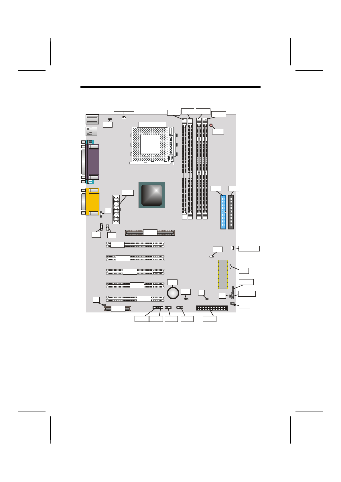
MMaaiinnbbooaarrdd CCoommppoonneenntts
s
CD2
J1
1
JP2
CPUFAN1
JP2
CPUFAN1
DDR1
CPU SOCKET
DDR2
DDR1 DDR2
DIMM1
DIMM1
DIMM2
DIMM2
LED1
LED1
JP4
IDE2
IDE 1
IDE 2
CASFAN1
CASFAN1
JP3
1111
JP3
SPKR1
1111
SPKR1PANEL1
J5
1111
1111
PANEL1
SIR1
J5
ATX1
ATX1
1
J2
J2
CD2
CD1
CD1
PCI1
AGP1
AGP1
IDE1
PCI1
PCI2
PCI2
PCI3
JP4
1111
PCI3
PCI4
PCI4
PCI5
J1
CNR1
PCI5
CNR1
BT1
BT1
JP1
J4
1111
JP1
1111
1111
USB2
USB3
WOL1WOM1
J4
FDD1
USB3 USB2WOL1WOM1
FDD1
4
Page 11

Table of Mainboard Components
Label Component
AGP1 Accelerated Graphics Port
ATX1 Power connector
BT1 Three volt realtime clock battery
CASFAN1 Auxiliary case cooling fan
CD1 Small (For Panasonic)
CD2 Big (For SONY)
CNR1 Communications Networking Riser slot
CPUFAN1 Cooling fan for CPU
DDR1~DDR2 Two 168 pin DDR SDRAM
DIMM1 ~ DIMM2 Two 184-pin DIMM sockets
FDD1 Floppy disk drive connector
IDE 1 Primary IDE channel
IDE 2 Secondary IDE channel
J1 Case open detection connector
J2 Front-oriented micr ophone/ lin e- out port hea der
J4 Sleep button connector
J5 Another Green LED Indicator for signal color
LED
JP1 Clear CMOS jumper
JP2 Keyboard and USB power on jumper
JP3 BIOS protection jumper
JP4 CPU frequency selection jumper
1
LED1
PANEL1 Connector for case front panel switches and
PCI1 ~ PCI5 Five 32-bit add-in card slots
SIR1 Serial infrared cable header
SOCKET 462 Socket A for AMD Athlon processor
SPEAKER Speaker connector
USB2/3 Front panel USB headers
WOL1 Wake On LAN wakeup connector
WOM1 Wake On Modem wakeup connector
Memory module LED
LED indicators
1
The red indicat or LED1 turns on if your system is s till powered, at which time memory modules cannot be installed or
uninstalled.
5
Page 12

CChhoooossiinngg aa CCoommppuutteerr CCaasse
There are many types of computer cas es on the market. T he
mainboard complies with the specifications for the ATX system case. Some f eatures on the mainb oard are implem ented
by cabling connectors on the mainboard to indicators and
switches on the s ystem case. Ensure that your case supports
all the features req uired. The mainboard can support one or
two floppy diskette drives and four enhanced IDE drives. Ensure that your case has sufficient po wer and space for all the
drives that you intend to install.
Most cases have a choice of I/O tem plates in the rear panel.
Make sure that the I/O template in the case matches the I/O
ports installed on the rear edge of the mainboard.
This mainboard has an ATX form factor of 240 x 304 mm.
Choose a case that accommodates this form factor.
This concludes Chapter 1. T he next chapter explains how to
install the mainboard.
e
6
Page 13

CChhaapptteerr 2
Installing the Mainboard
2
SSaaffeettyy PPrreeccaauuttiioonns
Follow these safety precautions when installing the mainboard:
• Wear a grounding strap attached to a grounded device
to avoid damage from static electricity.
• Discharge static electricity by touching the metal case
of a safely grounded object before working on the
mainboard.
• Leave components in the static-proof bags they came
in.
• Hold all circuit boards by the edges. Do not bend cir-
cuit boards.
s
Page 14

QQuuiicckk GGuuiidde
This Quick Guide suggests the steps you can tak e to assemble your system with the mainboard.
The following table pro vides a reference for installing specific
components:
e
Locating Mainboard Components
Setting Jumpers
Installing the Mainboard in a Case
Installing Case Components
Installing the CPU
Installing Memory
Installing an HDD and CD-ROM Drive
Installing an FDD
Installing Add-on Cards
Connecting Options
Connecting Peripheral (I/O) Devices
The appendix provides a quick reference for jumper
Note:
settings.
Go to page 4
Go to page 9
Go to page 13
Go to page 14
Go to page 16
Go to page 19
Go to page 21
Go to page 234
Go to page 245
Go to page 27
Go to page 30
8
Page 15

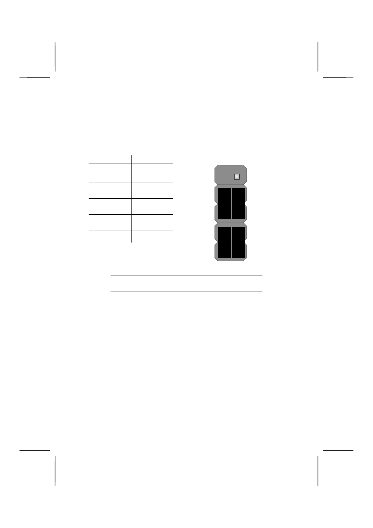
CChheecckkiinngg JJuummppeerr SSeettttiinnggs
This section explains how to set jumpers for correct configuration of the mainboard.
s
Setting Jumpers
Use the mainboard jumpers to set system configuration options. Jumpers with m ore than one pin are num bered. When
setting the jumpers, ensure that the jumper caps are placed
on the correct pins.
This illustration shows a 2-pin
jumper. When the jumper cap is
placed on both pins, the jumper is
SHORT. If you remove the jumper
cap, or place the jumper cap on
Short Open
just one pin, the jumper is OPEN.
This illustration shows a 3-pin
jumper. Pins 1 and 2 are SHORT.
1
2
3
9
Page 16
Checking Jumper Settings
J
The following illustr ation shows the location of the mainboard
jumpers. Pin 1 is labeled.
JP2
1111
CPUFAN1
JP2
1
ATX1
1
J2
CD2
CD1
AGP1
DDR1 DDR2
DIMM1
DIMM2
LED1
IDE1
IDE2
JP4
1111
PCI1
PCI2
PCI3
PCI4
BT1
PCI5
J1
CNR1
WOL1WOM1
1111
JP1
1111
1111
USB2
USB3
1111
J4
FDD1
CASFAN1
JP4
JP3
1111
JP3
1111
1111
SPKR1
J5
1111
PANEL1
1111
1111
P1
10
Page 17
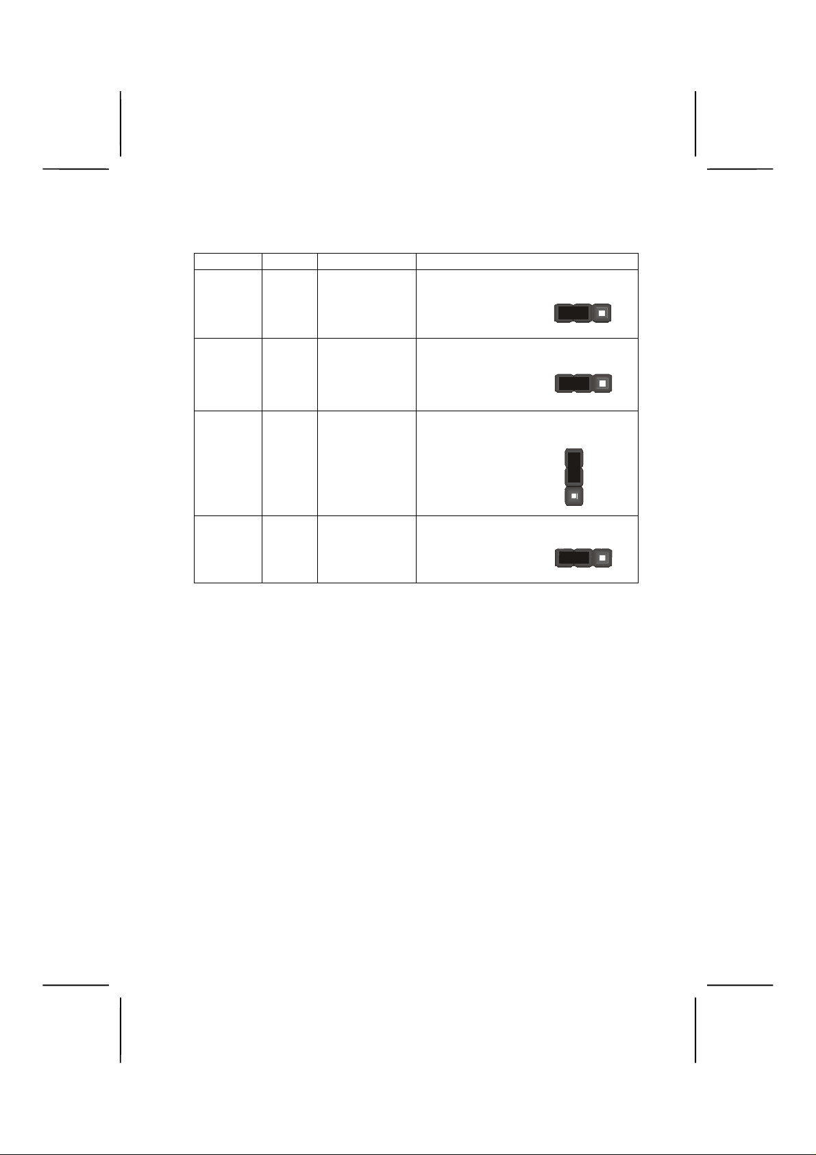
Jumper Settings
Jumper Type Description Setting (
JP1 3-pin Clear CMOS
JP2 3-pin K B Wake-Up
JP3 3-pin BIOS protec-
tion
JP4 3-pin CPU fre-
quency select
1-2: Normal
2-3: Clear
1-2: Enable
2-3: Disable
1-2: Disable
2-3: Enable
1-2: 100 MHz
2-3: 133 MHz
default
1
JP2
1
JP3
1
JP4
1
)
JP1
11
Page 18

Jumper 1
structions:
1. Turn the system off.
2. Short pins 2 and 3 on JP1.
3. Return the jumper to the normal setting.
4. Turn the system on. The BIOS is returned to the de-
Jumper 2
to awaken the system from power saving mode.
– enables you to c lear the BIOS. Follow these in-
fault settings.
– enable this jumper if you want ke yboard activity
Jumper 3
dated (flashed). Set the jumper to d isabled if you are going to
update your BIOS. After updating the BIOS, return it to the
default setting (enabled). For instructions on updating the
BIOS refer to Chapter 3.
Jumper 4
– enables you to prevent the BIOS f rom being up-
– Use this jumper to select the CPU frequency.
Editor’s Note:
Which setting should the user choose for CPU frequency. Should they also change the BIOS?
12
Page 19
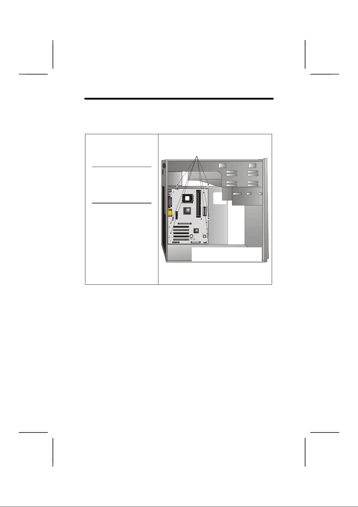
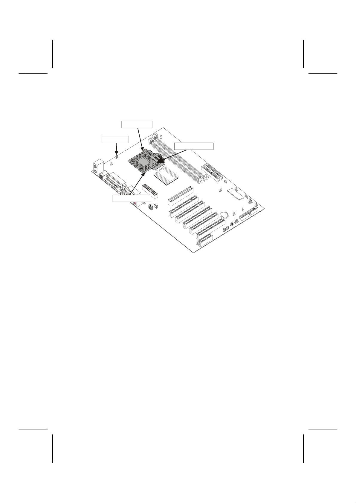
2. S
IInnssttaalllliinngg tthhee MMaaiinnbbooaarrdd iinn aa CCaasse
Refer to the following illus tration and instructi ons for installin g
the mainboard in a case:
e
This illustration shows
an example of a mainboard being installed in
a tower-type case:
Do not over-
Note:
tighten the
screws as this
can stress the
mainboard.
Most system cases have
mounting brackets installed in the case,
which correspond to the
holes in the mainboard.
Place the mainboard
over the mounting
brackets and secure the
mainboard onto the
mounting brackets with
screws.
Ensure that your c ase has an I/O tem plate that supports the
I/O ports and expansion slots on your mainboard.
ecure the mainboard with
screws where appropriate.
1. Place the mainboard
over the mounting brack ets.
13
Page 20
C
CCoonnnneeccttiinngg CCaassee CCoommppoonneenntts
After you have installed the m ainboard into a case, you can
begin connecting the mainboard components. Refer to the
following:
PUFAN1
s
AT X1
CPUFAN1
JP2
1
ATX1
1
J2
CD2
CD1
PCI1
PCI2
PCI3
PCI4
PCI5
J1
CNR1
AGP1
BT1
1111
USB3
WOL1WOM1
DIMM1
DIMM2
DDR1 DDR2
LED1
CASFAN1
IDE1
IDE2
CASFAN1
JP4
1111
1111
1111
JP1
J4
1111
USB2
FDD1
JP3
1111
J5
1111
PANEL1
SPKR1PANEL1
1111
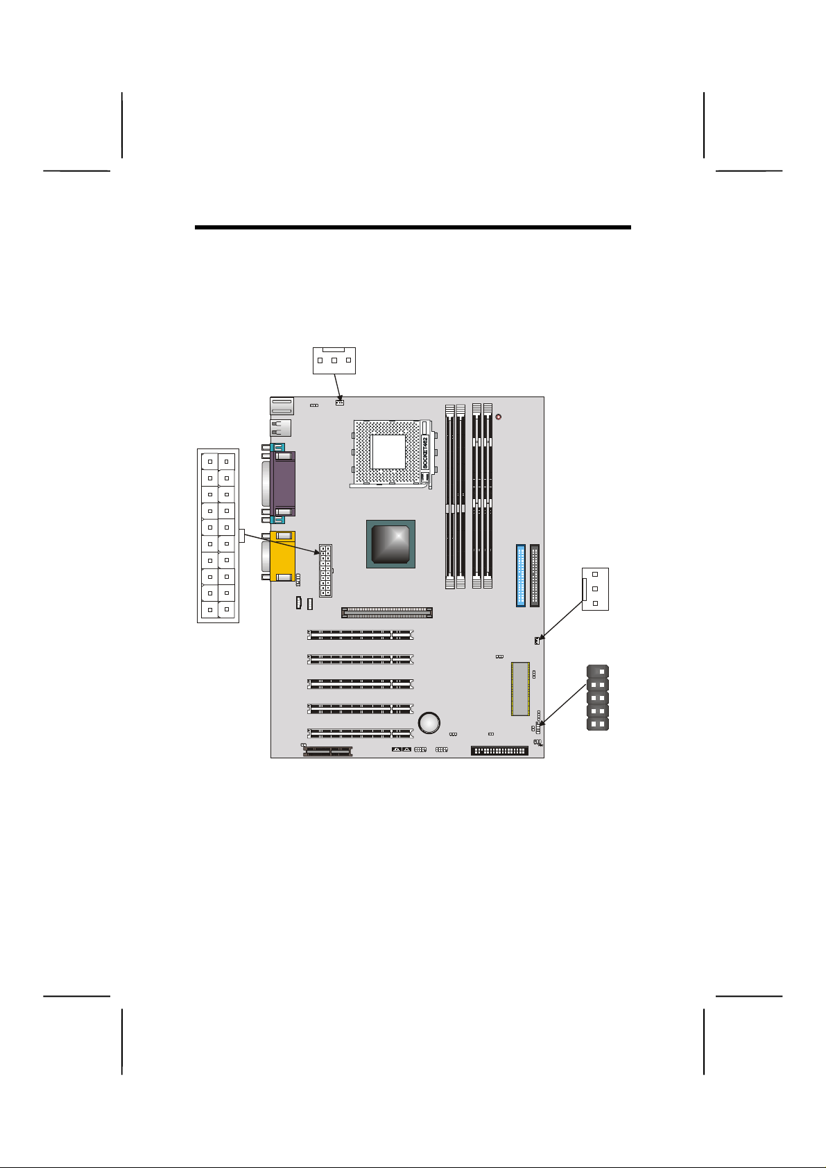
1. Connect the case power supply connector to ATX1.
2. Connect the CPU cooling fan cable to CPUFAN1.
3. Connect the case cooling fan connector to CASFAN1
1111
The following page explains how to make panel connections.
14
Page 21
The Panel Connector
h
The panel connector provides a standard set of switch and
LED connectors commonly found on ATX or micro-ATX cases.
Refer to the table below for information:
Device Pins
Empty 10
N/C 9
Power
6, 8
ON/OFF
Reset
5, 7
Switch
Green LED
2, 4
Indicator
HDD LED +1, -3
The plus sign (+ ) indicates a pin which must be con-
Note:
nected to a positive voltage.
Empty
(Pin 10)
Power Switch
(Pins 6, 8)
Green LED
(Pins 2, 4)
10 9
N/C
(Pin 9)
Reset Switc
(Pins 5, 7)
HDD LED
(Pins 1, 3)
2 1
15
Page 22

IInnssttaalllliinngg HHaarrddwwaarre
e
Installing the Processor
Caution:
make sure that you DO NOT scratch the mainboard or any
of the surface-mount resistors with the clip of the cooling
fan. If the clip of the cooling fan scrapes across the mainboard, you may cause serious damage to the mainboard or
its components.
On most mainboards, there are small surface-mount resistors near the processor socket, which may be damaged if
the cooling fan is carelessly install ed.
Avoid using cooling fans with sharp edges on the fan casing
and the clips. Also, install the cooling fan in a well-lit work
area so that you can clearly see the mainboard and processor socket .
When installing a CPU heatsink and cooling fan
Before installing the Processor
This mainboard autom atically determines the CPU clock frequency and system bus frequenc y for the process or. You m ay
be able to change these automatic settings by making
changes to jumpers on the mainboard, or changing the settings in the s ystem Setup Uti lity. We strongly recommend that
you do not overclock processors or other components to run
faster than their rated speed.
Warning:
the reliability of the system and introduce errors into your
system. Overclocking can permanently damage the mainboard by generating excess heat in components that are
run beyond the rated limits.
Overclocking components can adversely affect
This mainboard has a Socket 462 processor socket. When
choosing a process or, consider the perf ormanc e requirem ents
of the system. Per f orm anc e is bas ed on the processor desi gn,
the clock speed and system bus frequency of the processor,
and the quantity of inter nal cach e m em ory and ex terna l c ache
memory.
16
Page 23
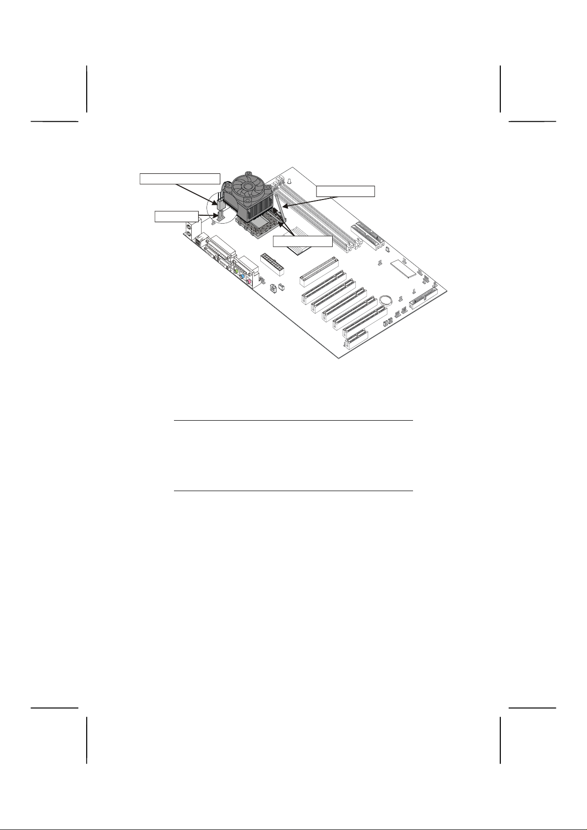
CPU Installation Procedure
The following illustration shows CPU installation components:
Socket 426
CPU fan
Pin A-1 c orner
Locking lever
Follow these instructions to install the CPU:
1. Pull the CPU socket locking lever away from the socket to unhook it and raise the locking lever to the upright
position.
2. Identify the pin A-1 corner on the CPU socket and the
pin A-1 corner on the processor.
3. Match the pin A-1 corners and insert the processor into
the socket. Do not use force.
4. Swing the locking lever down and hook it under the
latch on the edge of the socket.
5. Apply thermal grease to the top of the CPU.
17
Page 24
C
CPU fan connector
CPUFAN1
6. Lower the CPU fan/heatsink unit onto the CPU and
CPU socket and then snap the fan/heatsink into place.
7. Plug the CPU fan power cable into the CPU cooling
fan power supply on the mainboard (CPUFAN1).
After you have assembled the system, yo u must set
Note:
the correct clock speed and frontside bus (FSB)
speed. Check the jumper section in Appendix A if
your mainboard has jumpers that control the FSB,
and refer to Frequency/Voltage Control on page 61
for more information.
PU fan and
heatsink assembly
Locking lever
Pin A-1 corne r
18
Page 25

Installing Memory Modules
This mainboard accommodates 184-pin 2.5V unbuffered
Double Data Rate (DDR) or 168-pin 3.3V unbuffered Single
Data Rate (SDR) SDRAM memory modules. The memory
chips must be standard or registered SDRAM (Synchronous
Dynamic Random Access Memory).
The memory bus can run at 100 MHz or 133 MHz. If your
processor operates over a 100 MHz system bus, you can install PC100 or PC133 memory modules that operate over a
100 MHz or 133 MHz mem ory bus. If your proces sor op erat es
over a 133 MHz system bus, you can only install PC133
memory modules that operate over a 133 MHz memory bus.
SDRAM provides 800 MBps or 1 GBps data trans-
Note:
fer depending on whether the bus is 100 MHz or
133 MHz. Double Data Rate SDRAM (DDR
SDRAM) doubles the rate to 1.6 GBps and 2.1
GBps. DDR SDRAM uses additional power and
ground lines and requires 184-pin DIMM modules
rather than the 168-pin DIMMs used by SDRAM.
Installation Procedure
19
Page 26

The mainboard accommodates two SDR SDRAM and two
DDR SDRAM modules. You must ins tall at least one module
in any of the four slots. Each module can be installed with up
to 1 GB of memory; total memory capacity is 4 GB.
Refer to the following to install the memory modules.
1. Push the latches on each side of the DIMM slot down.
2. Align the memory module with the slot. The DIMM
slots are keyed with notches and the DIMMs are keyed
with cutouts so that they can only be installed correctly.
3. Check that the cutouts on the DIMM module edge
connector match the notches in the DIMM slot:
Latch
Cutout
Notch
Latch
Latch
Notches
Latch
DDR SDRAM Module SDR SDRAM Module
4. Install the DIMM module into the slot and press it firmly
down until it seats correctly. The slot latches are levered upwards and latch on to the edges of the DIMM.
5. Install any remaining DIMM modules.
Cutouts
20
Page 27

Installing a Hard Disk Drive/CD-ROM
This section describes how to install IDE devices such as a
hard disk drive and a CD-ROM drive.
About IDE Devices
Your mainboard has a primary and secondary IDE channel interface (IDE1 and IDE2 ). An IDE ribbon cabl e suppor ting two IDE
devices is bundled with t he mainbo a rd.
If you want to install m or e than two I DE de vices, get a se cond
IDE cable and you can add two more devices to the secondary IDE channel.
IDE devices have jumpers or switches tha t are used to s et the
IDE device as MASTER or SLAVE. Refer to the IDE device
user’s manual. When installing two IDE devic es on one cable,
ensure that one device is set to MASTER and the other device is set to S LAVE. The documentation of your IDE device
explains how to do this.
About UltraDMA
This mainboard su pports UltraDMA 66/ 100. UDMA is a technology that accelerates t he perform ance of devices in the IDE
channel. Install IDE d evices that support UD MA and use IDE
cables that support UDMA for better performance.
21
Page 28

Installing a Hard Disk Drive
1. Install the hard disk drive into the drive cage in your
ATX system case.
2. Plug the IDE cable into IDE1.
HDD
B
Colored
stripe
C
A
Pin 1
Ribbon cable connectors are usually keyed so that
Note:
they can only be installed correctly on the device
connector. If the connector is not keyed, make sure
that you match the pin-1 side of the cable connector
with the pin-1 side of the device connector. Each
connector has the pin-1 side clearly marked. The
pin-1 side of each ribbon cable is always marked
with a colored stripe on the cable.
3. Plug an IDE cable connector into the hard disk drive
IDE connector. It doesn't matter which connector on
the cable you use. Ensure that the pin-1 side of the
cable is matched with the pin-1 side of the connector.
Refer to the previous note.
4. Plug a power cable from the case power supply into
the power connector on the hard disk drive.
When you first start up your system, the BIOS should automatically detect your hard disk drive. If it doesn’t, enter the
Setup Utility and use the IDE Har d D isk Auto Detect feature to
configure the har d disk drive that you have installed. See IDE
HDD Auto-Detection on page 38 for more information.
22
Page 29

Installing a CD-ROM/DVD Drive
C
1. Install the CD-ROM/DVD drive into the drive cage in
your ATX system case.
2. Plug the IDE cable into IDE1 (A). If you have already
installed an HDD, use the other connector on the IDE
cable.
CD-ROM audio
connector
D
Ribbon cable connectors are usually keyed so that
Note:
they can only be installed correctly on the device
connector. If the connector is not keyed, make sure
that you match the pin-1 side of the cable connector
with the pin-1 side of the device connector. Each
connector has the pin-1 side clearly marked. The
pin-1 side of each ribbon cable is always marked
with a colored stripe on the cable.
D2
CD1
Colored
stripe
Pin 1
CD-ROM
B
A
C
3. Plug an IDE cable connector into the CD-ROM/DVD
drive IDE connector. It doesn't matter which connector
on the cable you use. Ensure that the pin-1 side of the
cable is matched with the pin-1 side of the connector.
Refer to the previous note.
4. Use the audio cable provided with the CD-ROM/DVD
drive to connect to the mainboard CD-in connector
CD1 or CD2.
23
Page 30

5. Plug a power cable from the case power supply into
the power connector on the CD-ROM/DVD drive.
When you first start up your system, the BIOS should automatically detect your CD-ROM/ DVD drive. If it doesn’t, enter
the Setup Utility and configure the CD-ROM/DVD drive that
you have install ed. See IDE Prim ary/Secondary Mast er/Slave
(Auto) on page 38 for more information.
Installing a Floppy Diskette Drive
The mainboard has a floppy diskette drive (FDD) interface
and ships with a diskette dr ive ribbon cable that s upports o ne
or two floppy diskette drives . You can i nstall a 5.25-inch drive
and a 3.5-inch drive with various c apacities. The floppy diskette drive cable has one type of connector for a 5.25-inch
drive and another type of connector for a 3.5-inch drive.
1. Install the FDD into the drive cage in your ATX system
case.
2. Plug the FDD cable into FDD1.
FDD
Colored
stripe
Ribbon cable connectors are usually keyed so that
Note:
they can only be installed correctly on the device
connector. If the connector is not keyed, make sure
that you match the pin-1 side of the cable connector
with the pin-1 side of the device connector. Each
connector has the pin-1 side clearly marked. The
pin-1 side of each ribbon cable is always marked
with a colored stripe on the cable.
24
B
C
A
Pin 1
Page 31

3. Plug the correct connector on the FDD cable for the
5.25-inch or 3.5-inch drive into the FDD connector (B).
4. Plug a power cable from the case power supply into
the power connector on the FDD.
When you first start up your system, go immediately to the
Setup Utility to configure the floppy diskette drives that you
have installed. See Dr ive A/Drive B (1.44M, 3.5 in ./None) on
page 39 for more information.
Installing Add-on Cards
This mainboard has five 32-bit PCI (Peripheral Components
Interconnect) expansion slots, one 4xAG P slot, and one CNR
slot.
AGP slot
PCI slots
CNR slot
4xAGP Slot
The 4xAGP slot is used to install a graphics
adapter that supports the 4xAGP specification and has a 4xAGP edge connector.
PCI Slots
PCI slots are used to install expansion cards
that have the 32-bit PCI interface.
CNR
The Communications Networking Riser
(CNR) slot can be used to insert a CNR card.
Before installing an add-in card, check the docu-
Note:
mentation for the card carefully. If the card is not
Plug and Play, yo u may ha ve to ma n ual l y con fi gur e
the card before installation.
CD2
CD1
PCI1
PCI2
PCI3
PCI4
PCI5
J1
CNR1
AGP1
WOL1WOM1
IDE
IDE2
CASFAN1
JP4
1111
JP3
1111
BT1
1111
1111
1111
USB2
USB3
J4
JP1
FDD1
1111
SPKR1PANEL1
J5
1111
1111
25
Page 32

1. Remove a blanking plate from the system case corresponding to the slot you are going to use.
2. Install the edge connector of the add-on card into the
expansion slot. Ensure that the edge connector is correctly seate d in the slot.
Add-on card
Edge connector
3. Secure the metal bracket of the card to the system
case with a screw.
For some add-on cards, for example graphics adap-
Note:
ters and net work adapters , you have to install
drivers and software be fore you can begin using the
add-in card.
26
Page 33

Connecting Optional Devices
3
5
Refer to the following for inf ormation on connectin g the mainboard’s optional device s:
CPUFAN1
JP2
1
J2
1111
J1
1
X
T
A
1
J2
CD2
CD1
PCI1
PCI2
PCI3
PCI4
PCI5
J1
CNR1
AGP1
BT1
1111
WOL1 WOM1
1111
DIMM1
DIMM2
DDR1 DDR2
LED1
E
D
2
E
D
SPEAKER
CASFAN1
JP4
1111
P
1111
R
K
P
S
1111
1
L
E
N
JP1
J4
1111
USB2 USB3
FDD1
A
P
1111
1111
1111
J5
J4
1111
WOLWOM
USB3
1111
USB2
1111
SIR1
J2: Front panel MIC/line-out
This header allows the user to install auxiliary front-oriented
microphone and line-out ports for easier access.
Pin Signal Name Pin Signal Name
AUD_RET_R
AUD_MIC
1
AUD_GND
2
AUD_MIC_BIAS
3
AUD_VCC
4
AUD_FPOUT_R
5
27
6
HP_ON
7
KEY
8
AUD_FPOUT_L
9
AUD_RET_L
10
Page 34

J1: Case open
This jumper prevents unauthorized access to your computer
by enabling an alarm that alerts you when your com puter case
has been opened.
J4:
Sleep button connector
J5: G-LED2
Editor’s Note:
Please supply the information for the items above.
USB2/USB3: USB port 3, 4 and 5, 6
The mainboard has two USB ports installed on the rear edge
I/O port array. Additionally, some com puter cases have USB
ports at the front of the case. If you h ave this kind of case, use
auxiliary USB connectors USB2 and USB3 to connect the
front-mounted ports to the mainboard.
Pin Signal Name Pin Signal Name
USB_FP_P1+
VREG_FP_USBPWR0
1
VREG_FP_USBPWR0
2
USB_FP_P0-
3
USB_FP_P1-
4
USB_FP_P0+
5
6
7
8
9
10
Ground
Ground
Key
USB_FP-OC0
WOL1/WOM: Wake On LAN/Wake On Modem
If you have installed a LAN card, use the c able provided with
the card to plug into t he m ainbo ard W O L1 connector. This enables the Wake On LAN (WOL) feature. W hen your s ystem is
in a power-saving mode, any LAN signal automatically resumes the system . You must enable this item us ing the Power
Management page of the Setup Utility.
Pin Signal Name
1
5VSB
2
Ground
3
SENSE
If you have installed a modem, use the cable provided with
28
Page 35

the modem to plug into th e mainboar d W OM1 connector. This
enables the Wake On Modem (WOM) feature. When your
system is in a power-saving mode, an y modem signal automatically resumes the system. You must enable this item
using the Power Managem ent page of the Setup Utility. See
Chapter 3 for more information.
SIR1: Serial infrared port
The mainboard supports a Serial Infrared (SIR) data port. Infrared ports allow the wireless exchange of information
between your com puter and similarly equipped d evices such
as printers, laptops, Personal Digital Assistants (PDAs), and
other computers.
Pin Signal Name
Not assigned
1
(No Pin)
2
+5V
3
Ground
4
IRTX
5
IRRX
6
SPEAKER1: Internal speaker
Connect the internal speaker connector to this header.
Pin Signal Name
1
SPKR
2
NC
3
Ground
4
+5V
29
Page 36

CCoonnnneeccttiinngg II//OO DDeevviiccees
s
The backplane of the mainboard has the following I/O ports:
PS/2
mouse
PS/2
keyboard
PS/2 Mouse
PS/2 Keyboard
USB Ports
LPT1
COM1/2
USB
ports
Pa ra lle l port (LPT1)
Serial port
COM 1
Serial port
COM 2
Game port
Use the upper PS/2 port to connect a
PS/2 pointing device.
Use the lower PS/2 port to connect a
PS/2 keyboard.
Use the USB ports to connect USB
devices.
Use LPT1 to connect printers or other
parallel communications devices.
Use the COM ports to connect serial
devices such as mice or fax/modems.
COM1 is identified by the system as
COM1/3. COM2 is identified by the
system as COM2/4.
Microphone
Line-in
Line-out
Game Port
Audio Ports
Use the game port to connect a joystick or a MIDI device.
Use the three audio ports to connect
audio devices. The left side jack is for
a stereo line-out signal. The middle
jack is for a stereo line-in signal. The
right side jack is for a microphone.
30
Page 37

External Connector Color Coding
Many connectors now use standard colors as shown in the
table below.
Connector Color
Analog VGA Blue
Audio line-in Light blue
Audio line-out Lime
Digital monitor/flat panel White
IEEE 1394 Grey
Microphone Pink
MIDI/game Gold
Parallel Burgundy
PS/2-compatible keyboard Purple
PS/2-compatible mouse Green
Serial Teal or Turquoise
Speaker out/subwoofer Orange
Right-to-left speaker Brown
USB Black
Video out Yellow
SCSI, network, telephone,
modem
None
This concludes Chapter 2. The next chapter covers the BIOS.
31
Page 38

Notes
32
Page 39

CChhaapptteerr 3
Using BIOS
3
AAbboouutt tthhee SSeettuupp UUttiilliitty
The computer uses the latest Award BIOS with support for
Windows Plug and Play. The CMOS chip on the mainboard
contains the ROM setup instructions f or configuring th e mainboard BIOS.
The BIOS (Basic Input and Output System) Setup Uti lity displays the system's configuration status a nd provides you with
options to set system parameters. T he parameters are s tored
in battery-backed-up CMOS RAM that saves this inform ation
when the power is turn ed off . When the s ystem is turned back
on, the system is configured with the values you stored in
CMOS.
The BIOS Setup Utility enables you to configure:
• Hard drives, diskette drives, and peripherals
• Video display type and display options
• Password protection from unauthorized use
• Power management features
The settings made in the Se tup Uti li t y aff ect how th e computer
performs. Befor e using the Setup Utility, ensure that you understand the Setup Utility options .
This chapter provides explanations for Setup Utility options.
y
Page 40

The Standard Configuration
A standard configuration has already been set in the Setup
Utility. However, we recommend that you read this chapter in
case you need to make any changes in the future.
This Setu p Utility should be used:
• when changing the system configuration
• when a configuration error is detected and you are
prompted to make changes to the Setup Utility
• when trying to resolve IRQ conflicts
• when making changes to the Power Management con-
figuration
• when changing the password or making other changes
to the Security Setup
34
Page 41

Entering the Setup Utility
When you power on the s ystem, BIOS enters the Po wer-On
Self Test (POST) routines. P OST is a series of built-i n diagnostics perform ed by the BIOS. After the POST routi nes are
completed, the following message appears:
Press DEL to enter SETUP
Pressing the delete ke y accesses the Award BIOS Setup
Utility:
CMOS Setup Utility – Copyright (C) 1984 – 2001 Award Software
Standard CMOS Features
Advanced BIO S Features
Advanced Chi pset Features
Integrated Peripherals
Power Management Setup
PnP/PCI Configurations
PC Health Stat us
Esc : Quit
F10 : Save & E xit Setup
Time, Date, Hard Disk Type . . .
Frequency/Voltage Control
Load Fail-Safe Def aul ts
Load Optimized Defa ul ts
Set Supervisor Password
Set User Password
Save & Exit Setup
Exit Without Saving
↑↑↑↑ ↓↓↓↓ →→→→
←←←←
: Select Item
BIOS Navigation Keys
The BIOS navigation keys are listed below:
Key Function
Esc Exits the current menu
←↑↓→
+/–
/PU/PD
F10 Saves the current configuration and exits setup
F1
F5 Loads previously saved values to CMOS
F6 Loads a minimum configuration for trouble-
F7 Loads an optimum set of values for peak per-
Scrolls through the items on a menu
Modifies the selected field's values
Displays a screen that describes all key functions
shooting.
formance
35
Page 42

Updating the BIOS
You can download and install updated BIOS for this mainboard from the m anufacturer's Web site. New BIO S provides
support for new peripher als, im provem ents in perf orm ance, or
fixes for known bugs. Install new BIOS as follows:
1. If your mainboard has a BIOS protection jumper,
change the setting to allow BIOS flashing. (Refer to
Appendix A for jumper settings.)
2. If your mainboard ha s an item called Firmware Write
Protect in Advanced BIOS features, disable it. (Firmware
Write Protect prevents BIOS from being overwritten.)
3. Create a bootable system disk. (Refer to Windows online help for information on creating a bootable system
disk.)
4. Download the Flash Utility and new BIOS file from the
manufacturer's Web site. Copy these files to the system diskette you created in Step 3.
5. Turn off your computer and insert the system diske tte in
your computer's diske tte drive. (You might need to run
the Setup Utility and change the boot priority items on the
Advanced BIOS Featu r e s Setu p pag e, to fo rce y ou r
computer to boot fro m the floppy diskette drive fi rst.)
6. At the A:\ prompt, type the Flash Utility program name
and press <Enter>. You see a screen similar to the
following:
(C) Award Software 1999 All Rights Reserved
For (MAINBOARD NAME) DATE: 10/26/2000
Flash Type
File Name to Program :____________________
Error Message
FLASH MEMORY WRITER V7.33
7. Type the filename of the new BIOS in the “File Name
to Program” text box. Follow the onscreen directions to
update the mainboard BIOS.
8. When the installation is complete, remove the floppy
diskette from the diskette drive and restart your computer. If your mainboard has a Flash BIOS jumper,
reset the jumper to protect the newly installed BIOS
from being overwritten.
36
Page 43

UUssiinngg BBIIOOS
S
When you start the Setup Uti lity, the main menu appears. The
main menu of the Setup Utility displays a list of the options
that are available. A highlight indicates which option is currently selected. Use the cursor arrow keys to move the
highlight to other opt ions. When an option is highlig hted, execute the option by pressing <Enter>.
Some options lead to pop- up dialog boxes tha t prompt you to
verify that you wish to exec ute that opt ion. Oth er options lead
to dialog boxes that prompt you for information.
Some options (marked with a triangle
) lead to submenus
that enable you to change the values for the option. Use the
cursor arrow keys to scroll through the items in the submenu.
In this manual, default values are enclosed in parenthesis.
Submenu items are denoted by a triangle
.
Standard CMOS Features
This option displays basic information about your system.
CMOS Setup Utility – Copyright (C) 1984 – 2001 Award Software
Date (mm:dd:yy) Tue, July 11 2000
Time (hh:mm:ss) 12 : 8 : 59
IDE Primary Master
IDE Primary Slave
IDE Secondar y Master
IDE Secondary Slave
Drive A [1.44M, 3.5 in.]
Drive B [None]
Floppy 3 Mode Support [Disabled]
Video [EGA/VGA]
Halt On [All Errors]
Base Memory 640K
Extended Memory 65535K
Total Memory 1024K
Standard CMOS Features
Item Help
Menu Level
Change the da y, month,
year and century.
↑↑↑↑ ↓↓↓↓ →→→→ ←←←←
: Move Enter : Select +/-/PU/PD:Value: F10: Save ESC: Exit F1:General Help
F5:Previous Values F6:Fail-Safe Defaults F7:Optimized Defaults
37
Page 44

Date and Time
The Date and Time items show the curren t date and time on
the computer. If you are running a Windows OS, these items
are automaticall y upda ted wh e ne ver you make changes to the
Windows Date and Time Properties utility.
IDE Devices (None)
Your computer has two IDE channels (Primary and Secondary)
and each channel can be installed with one or two devices
(Master and Slave). Use these it ems to configure eac h device
on the IDE channel.
Press <Enter> to display the IDE sub-menu:
CMOS Setup Utility – Copyright © 1984 – 2000 Award Software
IDE HDD Auto-Detection Press Enter
IDE Primary Master [Auto]
Access Mode [Auto]
Capacity 0 MB
Cylinder 0
Head 0
Precomp 0
Landing Zone 0
Sector 0
IDE Primary Master
Item Help
Menu Level
To auto-detect the
HDD’s size, head . . . on
this channel
↑↑↑↑ ↓↓↓↓ →→→→ ←←←←
: Move Enter : Select +/-/PU/PD:Value: F10: Save ESC: Exit F1:General Help
F5:Previous Values F6:Fail-Safe Defaults F7:Optimized Defaults
IDE HDD Auto-Detection
Press <Enter> while th is it em is high lighte d to pr om pt the Setup Utility to automatic ally detect and configure an ID E device
on the IDE channel.
If you are setting up a new hard disk drive that sup-
Note:
ports LBA mode, more than one line will appear in
the parameter box. Choose the line that lists LBA
for an LBA drive.
IDE Primary/Secondary Master/Slave (Auto)
Leave this item at Auto to enable the system to automatically
detect and c onf ig ur e IDE dev ic es on th e ch ann el. If it f ails to f ind
a device, change the value to Manual and then manually configure the drive by entering the characteristics of the drive in the
items described below.
38
Page 45

Refer to your drive's docum ent at i on or look on t h e drive cas i n g if
you need to obtain this information. If no device is installed,
change the value to None.
Before attempting to configure a hard disk drive,
Note:
ensure that you have the configuration infor mation
supplied by the manufacturer of your hard drive. Incorrect settings can result in your system not
recognizing the installe d hard disk.
Access Mode
This item defines ways that can be used to access IDE hard
disks such as LBA (Large Block Addressing). L ea ve t his value
at Auto and the system will automatically decide the fastest
way to access the hard disk drive.
Press <Esc> to return to the Standard CMOS Features page.
Drive A/Drive B (1.44M, 3.5 in./None)
These items define the characteristics of any diskette drive
attached to the system . You can con nect one or two diskette
drives.
Floppy 3 Mode Support (Disabled)
Floppy 3 mode refer s to a 3.5-inch diskette with a c apacity of
1.2 MB. Floppy 3 mode is sometimes used in Japan.
Video (EGA/VGA)
This item defines the video mode of the system. T his mainboard has a built-in VG A gr a ph ics s ystem; you must leave this
item at the default value.
Halt On (All Errors)
This item defines the operation of the system POST (Power
On Self Test) routine. You can use this item to select which
types of errors in the POST are sufficient to halt the system.
Base Memory, Extended Memory, and Total Memory
These items are autom atically detecte d by the s ystem at star t
up time. These are display-only fields. You cannot make
changes to these fields.
39
Page 46

Advanced BIOS Setup Option
This option displays advanced information about your system.
CMOS Setup Utility – Copyright (C) 1984 – 2001 Award Software
Anti-Virus Protection [Disabled]
Y2K Monitor [Disa bled]
CPU Internal C ache [Enabled]
External Cache [Enabl ed]
CPU L2 Cache ECC Checking [Enabled]
Processor Number Feature [Enabled]
Quick Power On Self Test [Enabled]
First Boot Device [Floppy]
Second Boot D evice [HDD-0]
Third Boot Device [LS120]
Boot Other Device [Enabled]
Swap Floppy Drive [Disabled]
Boot Up Floppy Seek [Enabled]
Boot Up NumLock Statu s [ On]
Gate A20 Option [Fast]
Typematic Rate Setting [Disabled]
x Typematic Rate (Chars/Sec) 6
x Typematic Delay (Msec) 250
Security Option [Setup]
↑↑↑↑ ↓↓↓↓ →→→→ ←←←←
: Move Enter : Select +/-/PU/PD:Value: F10: Save ESC: Exit F1:General Help
F5:Previous Values F6:Fail-Safe Defaults F7:Optimized Defaults
Anti-Virus Protection (Disabled)
When enabled, this item provides protection against viruses
that try to write to the boot sector and partit ion table of your
hard disk drive. You need to disable this item when installing
an operating system. We recommend that you enable this
item as soon as you have installed an operating system.
Advanced BIO S Features
Menu Level
Allows you to choose
the VIRUS warni ng
feature for IDE Hard
Disk boot sector
protection. If this
function is enabled
and someone attempts
to write data into this
area, BIOS will show a
warning message on
screen and alarm beep
Item Help
For complete protection against viruses, install viru s
Note:
software in your operating system and update the virus definitions regularly.
Y2K Monitor (Disabled)
Enable this item to a llow the s ystem to m onitor for errors generated by the year 2000 bug.
CPU Internal Cache CPU Internal Cache (Enabled)
All processors that can be installed in th is mainboard use internal level 1 (L1) cache memory to improve performance.
Leave this item at the default value for better performance.
40
Page 47

External Cache (Enabled)
Most processors that can be installed in this system us e external level 2 (L2) cache memory to improve performance.
Leave this item at the default value for better performance.
CPU L2 Cache ECC Checking (Enabled)
This item enables or disables ECC (Error Correction Code) error checking on the CPU cache m emory. We recommend that
you leave this item at the default value.
Processor Number Feature (Enabled)
Some new processors are installed with a unique processor
number. This number may be used for verificat ion in Internet
transactions and e-com merce. If you prefer not to use or distribute the unique processor number, disable this item to
suppress the processor number.
Quick Power On Self Test (Enabled)
Enable this item to shorten the power on testing (POST) and
have your system start up faster. You might like to enable this
item after you are confide nt that your system hardware is operating smoothly.
First/Second/Third Boot Device (Floppy/HDD-0/LS120)
Use these three items to select the priority and order of the
devices that your system searches for an operating s ystem at
start-up time.
Boot Other Device (Enabled)
When enabled, the system searches all other possible locations for an operating system if it fails to find one in the
devices specified under th e First, Second, and Third boo t devices.
Swap Floppy Drive (Disabled)
If you have two flopp y disk ette drives i n your s ystem , this item
allows you to swap the ass igned drive letters so that drive A
becomes drive B, and drive B becomes drive A.
41
Page 48

Boot Up Floppy Seek (Enabled)
If this item is enabled, it checks the size of the floppy disk
drives at start-up time. You don't need to enable this item unless you have a legacy diskette drive with 360K capacity.
Boot Up NumLock Status (On)
This item defines if the keyboard Num Lock key is active when
your system is started.
Gate A20 Option (Fast)
This item defines how the system handles legacy software
that was written for an ear lier g eneratio n of process ors. Le ave
this item at the default value.
Typematic Rate Setting (Disabled)
If this item is enabled, you can use the following two items to
set the typematic rate and the typematic delay settings for
your keyboard.
Typematic Rate (Chars/Sec):
•
how many characters per second are generated by a
held-down key.
Typematic Delay (Msec):
•
many milliseconds must elapse before a held-down
key begins generating repeat characters.
Use this item to define
Use this item to define how
Security Option (Setup)
If you have installe d password protection, this item defines if
the password is require d at system star t up, or if it is onl y required when a user tries to enter the Setup Utility.
OS Select For DRAM > 64 MB (Non-OS2)
This item is only requir ed if you have installed more than 64
MB of memory and you are runni ng the OS/2 operating system. Otherwise, leave this item at the default.
HDD S.M.A.R.T Capability (Disabled)
The S.M.A.R.T. (Self-Monitoring, Analysis, and Reporting
Tec hnology) system is a diagnos tics technology tha t monitors
and predicts device per form ance. S.M.A.R.T. software resides
on both the disk drive and the host computer.
42
Page 49

The disk drive sof tware monitors the internal perf ormance of
the motors, media, heads, and electronics of the drive. The
host software monitors the overall reliability status of the drive.
If a device failure is predicted, the host software, through the
Client WORKS S.M.A.R.T applet, warns the user of the impending condition and advises appropriate action to protect
the data.
Report No FDD For WIN95 (Yes)
If you are running a system with no floppy drive and using
Windows 95, select Yes for this item to ensure compatibility
with the Windows 95 logo certification. Otherwise, select No.
Advanced Chipset Features Option
These options define critical timing parameters of the mainboard. Yo u sh ould l eave t he item s on this p age at t heir defau lt
values unless you are very familiar with the technical s pecifications of your system hardware. If you change the values
incorrectly, you may introduce fatal errors or recur ring inst ability into your system.
CMOS Setup Utility – Copyright (C) 1984 – 2001 Award Software
DRAM Clock/Drive Control [Press Enter]
AGP & P2P Bridge Control [Press Enter]
CPU & PCI Bus Control [Press Enter]
Memory Hole [Disabled]
System BIOS Cacheable [Enabled]
Video RAM Cacheable [Enabled]
Advanced Chi pset Features
Item Help
Menu Level
↑↑↑↑ ↓↓↓↓ →→→→ ←←←←
: Move Enter : Select +/-/PU/PD:Value: F10: Save ESC: Exit F1:General Help
F5:Previous Values F6:Fail-Safe Defaults F7:Optimized Defaults
Editor’s Note:
When we try to access the DRAM Clock/Drive Control submenu, the system crashes, so we could not
verify the items below. Please check them for us.
43
Page 50

DRAM Clock/Drive Control
Scroll to this item and press <Enter> to view the following
screen:
CMOS Setup Utility – Copyright (C) 1984 – 2001 Award Software
Current FSB Frequency
Current DRAM Frequency
DRAM Clock [100 MHz]
DRAM Timing [By SPD]
x SDRAM Cycle Length 3
x Bank Interleave Disabled
DRAM Command Rate [2T Command]
↑↑↑↑ ↓↓↓↓ →→→→ ←←←←
: Move Enter : Select +/-/PU/PD:Value: F10: Save ESC: Exit F1:General Help
F5:Previous Values F6:Fail-Safe Defaults F7:Optimized Defaults
Current FSB Frequency
This item displa ys the fr ontside b us ( FSB) f requ enc y. This is a
display-only item. You cannot make changes to this field.
Current DRAM Frequency
This item displa ys the memory (DRAM) frequency. This is a
display-only item. You cannot make changes to this field.
DRAM Clock/Dri ve Control
Menu Level
Item Help
DRAM Clock (100 MHz)
This item enables you to m anually set the DRAM Clock. We
recommend that you leave this item at the default value.
DRAM Timing (By SPD)
Set this to the default va lue to enable the s ystem to autom atically set the SDR AM tim ing b y SPD (Seri al Presenc e Det ect).
SPD is an EEPROM c hip on the DI MM module th at stores information about the m emory chips it contains, inc luding size,
speed, voltage, row and column addresses, and manufacturer.
If you disable this item, you can us e the following three item s
to manually set the timing parameters for the system memory
SDRAM Cycle Length (3)
When synchronous DRAM is installed, the number of clock
44
Page 51

cycles of CAS latency depen ds on the DRAM timing. We recommend that you leave this item at the default value.
Bank Interleave (Disabled)
Enable this item to increase memory speed. When enabled,
separate memor y banks are set for odd and even ad dresses
and the next byte of m emory can be accessed whil e the current byte is being refreshed.
DRAM Command Rate (2T Command)
This item enables you to specify the waiting tim e for the CPU
to issue the next c ommand after issuing the command to t he
DDR memory. We recommend that you leave this item at the
default value.
Press <Esc> to return to the Advanced Chipset Features page.
AGP & P2P Bridge Control
Scroll to this item and press <Enter> to view the following
screen:
CMOS Setup Utility – Copyright (C) 1984 – 2001 Award Software
AGP Aperture Si ze [64M]
AGP Mode [4X]
AGP Driving Control [Auto]
x AGP Driving Value DA
AGP Fast Write [Disabled]
AGP Master 1 WS Wri te [Disabled]
AGP Master WS Read [Disabled]
AGP & P2P Bridge Control
Item Help
Menu Level
↑↑↑↑ ↓↓↓↓ →→→→ ←←←←
: Move Enter : Select +/-/PU/PD:Value: F10: Save ESC: Exit F1:General Help
F5:Previous Values F6:Fail-Safe Defaults F7:Optimized Defaults
AGP Aperture Size (64 MB)
This item defines the size of the aperture if you use an AGP
graphics adapter. The AGP aperture ref ers to a s ection of the
PCI memory address range used for graphics memory. We
recommend that you leave this item at the default value.
AGP Mode (4X)
This item allows you to enable or disable the c aching of display data for the pr ocessor video memor y. Enabling AGP-4X
45
Page 52

Mode can greatly improve the displ a y speed . Dis a bl e this item
if your graphics display card does not support this feature.
AGP Driving Control (Auto)
This item is used to signal driving current on AGP cards to
auto or manual. Som e AGP cards need s tronger than norm al
driving current in order to operate. We recommend that you
set this item to the default.
AGP Driving Value:
•
to Manual, use this item to set the AGP current driving
value.
AGP Fast Write (Disabled)
This item lets you enable or disable the caching of display data
for the video memory of the processor. Enabling this item can
greatly improve the display speed. Disable this item if your
graphics display card does not support this feature.
AGP Master 1 WS Write (Disabled)
This implements a sing le delay when writing to the AG P Bus.
By default, two-wait s tates are used by the s ystem, providing
greater stability.
AGP Master 1 WS Read (Disabled)
This implements a s ingle del ay whe n rea ding to the AGP Bus.
By default, two-wait states are used by the system, allowi ng
for greater stability.
When AGP Driving Control is set
Press <Esc> to return to the Advanced Chipset Features page.
46
Page 53

CPU & PCI Bus Control
Scroll to this item and press <Enter> to view the following
screen:
CMOS Setup Utility – Copyright (C) 1984 – 2001 Award Software
PCI1 Master 0 WS Write [Enabled]
PCI2 Master 0 WS Write [ Enabled]
PCI1 Post Write [Enabled]
PCI2 Post Write [Enabled]
PCI Delay Transaction [Disabled]
↑↑↑↑ ↓↓↓↓ →→→→ ←←←←
: Move Enter : Select +/-/PU/PD:Value: F10: Save ESC: Exit F1:General Help
F5:Previous Values F6:Fail-Safe Defaults F7:Optimized Defaults
PCI 1/2 Master 0 WS Write (Enabled)
When enabled, writes to the PCI bus are executed with zero
wait states, providing faster data transfer.
PCI 1/2 Post Write (Enabled)
When enabled, writes f rom the CPU to PCU b us are buff ered,
to compensate for the speed differences between the CPU
and PCI bus. When disabled, the writes are not buffered and
the CPU must wait until t he write is complete before starting
another write cycle.
AGP & P2P Bridge Control
Menu Level
Item Help
PCI Delay Transaction (Disabled)
The mainboard’s chi pset has an embedded 32-bit pos t write
buffer to support delay transact ions cycles. Select Enabled to
support compliance with PCI specification version 2.1.
Press <Esc> to return to the previous screen.
Memory Hole (Disabled)
This item is us ed to reser ve mem ory space f or ISA ex pansion
cards that require it.
System BIOS/Video RAM Cacheable (Enabled)
These items allow the video and system to be cached in
memory for faster execution . Leave these items at the default
value for better performance.
47
Page 54

Integrated Peripherals Option
These options define th e operation of peripheral com ponents
on the system's input/output ports.
CMOS Setup Utility – Copyright (C) 1984 – 2001 Award Software
OnChip IDE Device [Press Enter]
OnChip PCI Device [Press Enter]
Super I/O Device [Press Enter]
Init Display First [PCI Slot]
OnChip USB Controller [All Enabled]
USB keyboard Support [Disabled]
IDE HDD Block M ode [Enabled]
PWRON After PWR-Fail [off]
↑↑↑↑ ↓↓↓↓ →→→→ ←←←←
: Move Enter : Select +/-/PU/PD:Value: F10: Save ESC: Exit F1:General Help
F5:Previous Values F6:Fail-Safe Defaults F7:Optimized Defaults
OnChip IDE Device
Scroll to this item and press <Enter> to view the following
screen:
CMOS Setup Utility – Copyright (C) 1984 – 2001 Award Software
OnChip IDE Channel0 [Enabled]
OnChip IDE Channel1 [Enabled]
IDE Prefetch Mode [Enabled]
Primary Master PIO [Auto]
Primary Slave PIO [Auto]
Secondary Master PIO [Auto]
Secondary Slave PIO [Auto]
Primary Master UDMA [Auto]
Primary Slave UDMA [Auto]
Secondary Master UDMA [Auto]
Secondary Slave UDMA [Auto]
Integrated Peripherals
Menu Level
OnChip IDE Devi ce
Menu Level
Item Help
Item Help
↑↑↑↑ ↓↓↓↓ →→→→ ←←←←
: Move Enter : Select +/-/PU/PD:Value: F10: Save ESC: Exit F1:General Help
F5:Previous Values F6:Fail-Safe Defaults F7:Optimized Defaults
On-Chip IDE Channel 0/1 (Enabled)
Use these items to enable or disable the PCI IDE channels
that are integrated on the mainboard.
48
Page 55

IDE Prefetch Mode (Enabled)
The onboard IDE drive interfaces supports IDE prefetching,
for faster drive acces s. If you install a pr imary and secondar y
add-in IDE interfac e, set this field to Disabled if the interface
does not support prefetching.
IDE Primary/Secondary Master/Slave PIO (Auto)
Each IDE channel supports a master device and a slave device. These four items let you assign which kind of PIO
(Programmed Input/Output) is used by IDE devices. Choose
Auto to let the system auto detect which PIO mode is best , or
select a PIO mode from 0-4.
IDE Primary/Secondary Master/Slave UDMA (Auto)
Each IDE channel supports a master device and a slave device. This mainboard supports UltraDMA technology, which
provides faste r access to IDE devices.
If you install a device that sup ports UltraDMA, cha nge the appropriate item on this list to Auto. You may have to install the
UltraDMA driver suppli ed with this mainboard in order to us e
an UltraDMA device.
Press <Esc> to return to the Integrated Peripherals screen.
OnChip PCI Device
Scroll to this item and press <Enter> to view the following
screen:
CMOS Setup Utility – Copyright (C) 1984 – 2001 Award Software
OnChip AC97 Audio [Auto]
VIA-3068 MC97 Modem [Auto]
↑↑↑↑ ↓↓↓↓ →→→→ ←←←←
: Move Enter : Select +/-/PU/PD:Value: F10: Save ESC: Exit F1:General Help
F5:Previous Values F6:Fail-Safe Defaults F7:Optimized Defaults
OnChip PCI Devi ce
Menu Level
49
Item Help
Page 56

OnChip AC97 Audio (Auto)
Enables and disables the onboard audio chip. Disable this
item if you are going to install a PCI audio add-in card.
VIA-3068 MC97 Modem (Auto)
Enables and disables the onboard modem . Disable this item if
you are going to install an external modem.
Press <Esc> to return to the Integrated Peripherals screen.
SuperIO Device
Scroll to this item and press <Enter> to view the following
screen:
CMOS Setup Utility – Copyright (C) 1984 – 2001 Award Software
Onboard FDC Control l er [Enabled]
Onboard Serial Port 1 [3F8/IRQ4]
Onboard Serial Port 2 [2F8/IRQ3]
UART Mode Select [Normal]
UR2 Duplex Mode [Half]
Onboard Parallel Port [378/IRQ7]
Parallel Port Mode [ECP]
ECP Mode Use DMA [3]
Game Port Address [201]
Midi Port Address [33 0]
Midi Port IRQ [10]
SuperIO Device
Item Help
Menu Level
↑↑↑↑ ↓↓↓↓ →→→→ ←←←←
: Move Enter : Select +/-/PU/PD:Value: F10: Save ESC: Exit F1:General Help
F5:Previous Values F6:Fail-Safe Defaults F7:Optimized Defaults
Onboard FDC Controller (Enabled)
This option enables the onboard floppy disk drive controller.
Onboard Serial Port 1 (3F8/IRQ4)
This option is used to ass ign the I/O addres s and interrupt request (IRQ) for the onboard serial port 1 (COM1).
Onboard Serial Port 2 (2F8/IRQ3)
This option is used to ass ign the I/O addres s and interrupt request (IRQ) for the onboard serial port 2 (COM2).
50
Page 57

UART Mode Select (Normal)
This field is ava ilabl e if the Onboard Seri al Por t 2 f iel d is s et to
any option but Disabled. UART Mode Select enables you to
select the infrared communication protocol: Normal (default),
IrDA, or ASKIR. IrDA is an infrared communication protocol
with a maximum baud r ate up to 115.2K bps. ASKIR is Shar p's infrared communication protocol with a maximum baud
rate up to 57.6K bps.
UR2 Duplex Mode (Half)
This field is available when UART 2 Mode is set to either
ASKIR or IrDA. This item enables you to determ ine the infrared function of the onb oard infrar ed chip. The op tions are Ful l
and Half (default).
Full-duplex means that you can trans mit and send inform ation
simultaneously. Half-duplex is the tra nsm ission of data in both
directions, but only one direction at a time.
Onboard Parallel Port (378/IRQ7)
This option is used to ass ign the I/O addres s and interrupt request (IRQ) for the onboard parallel port.
Parallel Port Mode (ECP)
Enables you to set the da ta transfer protocol for your parallel
port. There are four options: SPP (Standard Parallel Port),
EPP (Enhanced Parallel Port), ECP (Extended Capabilities
Port) and ECP+EPP.
SPP allows data output only. Extended Capabilities Port (ECP)
and Enhanced Parallel Port (EPP) are bi-directional modes, allowing both data input and outp ut . ECP and EPP mode s are only
supported with EPP - an d E C P-awa re pe ri p h erals.
51
Page 58

ECP Mode Use DMA (3)
When the onboard paral lel port is set to ECP mode, the p arallel port can use DMA 3 or DMA 1.
Game Port Address (201)
This item sets the I/O address for the game port.
Midi Port Address (330)
This item sets the I/O address for the Midi function.
Midi Port IRQ (10)
This item sets the interrupt request for the Midi function.
Press <Esc> to return to the Integrated Peripherals screen.
Init Display First (PCI Slot)
Use this item to specify whether your gr aphics adapter is installed in one of the PCI slots or is integrated on the
mainboard.
OnChip USB Controller (All Enabled)
Enable this item if you plan to use the Universal Serial Bus
ports on this mainboard.
USB Keyboard Support (Disabled)
Enable this item if you plan to use a keyboard connected
through the USB port in a legacy operating system (s uch as
DOS) that does not support Plug and Play.
IDE HDD Block Mode (Enabled)
Enable this field if your IDE hard drive supports block mode.
Block mode enables BIOS to automatically detec t the optimal
number of block read and writes per sector that the drive c an
support and improves the speed of access to IDE devices.
PWRON After PWR-Fail (Off)
This item determines the power state after a power failure. Set
this item to On to enable your computer to autom atically restart after a power failure
52
Page 59

Power Management Setup Option
This option lets you control system power m anagement. The
system has various power-saving modes including powering
down the hard disk, tur ning off the video, suspendin g to RAM,
and software power down that a llows the system to be automatically resumed by certain events.
The power-saving m odes can be c ontrolled by tim eouts. If the
system is inactive for a time, the timeouts begin counting. If
the inactivity continues so that th e timeout per iod ela pses, the
system enters a power- saving mode. If any item in the list of
Reload Global Timer Events is Enabled, then any activit y on
that item will reset the timeout counters to zero.
If the system is suspended, or has been powered down by
software, it can be resum ed b y a wake up call t hat is gen erated by incoming traffic to a m odem, a LAN card, a PCI c ard, or
a fixed alarm on the system realtime clock,
CMOS Setup Utility – Copyright (C) 1984 – 2001 Award Software
ACPI function [Enabled]
ACPI Suspend Type [S1(POS)]
Power Management Option [User Define]
HDD Power Down [Disable]
Suspend Mode [Disable]
Video Off Option [Suspend --> Off]
Video Off Method [DPMS Support]
MODEM Use IRQ [ 3]
Soft-Off by PWRBTN [Instant-Off]
IRQ/Event Activity Detect [Press Enter]
Power Management Setup
Item Help
Menu Level
↑↑↑↑ ↓↓↓↓ →→→→ ←←←←
Help F5:Previous Values F6:Fail-Safe Defaults F7:Optimi zed Defaults
: Move Enter : Select +/-/PU/PD:Value: F10: Save ESC: Exit F1:General
53
Page 60

ACPI Function (Enabled)
This mainboard supports ACPI (Advanced Configuration and
Power management In terface) . Use this item to enable or dis able the ACPI feature.
ACPI is a power management specification that
Note:
makes hardware status information available to the
operating system. ACPI enables a PC to turn its
peripherals on and off for improved power management. It also allows the PC to be turned on and
off by external devices, so that mouse or keyboard
activity wakes up the co mp ute r.
ACPI Suspend Type (S1(POS))
Use this item to define how your s ystem suspends. In the default, S1(POS), the s uspend mode is equivalent to a software
power down. If you select S3 (STR), the suspend mode is a
suspend to RAM, i.e., the s ystem shuts do wn with the exception of a refresh current to the system memory.
Power Management Option (User Define)
This item acts like a master switch for the power-saving
modes and hard dis k timeouts. If this item is s et to Max Saving, power-saving modes occur after a short timeout. If this
item is set to Min Saving, po wer-saving modes occur after a
longer timeout. If the item is set to User Def ine, you can insert
your own timeouts for the power-saving modes.
HDD Power Down (Disable)
The IDE hard drive will spin do wn if it is not acc essed within a
specified length of tim e. Options ar e f rom 1 Min t o 15 Mi n and
Disable.
Suspend Mode (Disable)
The CPU clock will be stopped and the video signal will be
suspended if no Power Management events occur for a
specified length of tim e. Full power f unction will retur n when a
Power Management eve nt is detected. Options ar e f r om 1 Min
to 1 Hour and Disable.
54
Page 61

Video Off Option (Suspend --> Off)
This option defines if the video is powered down when the
system is put into suspend mode.
Video Off Method (DPMS Support)
This item defines how the video is powered down to save
power. This item is set to DPMS (D ispla y Power Ma nagement
Software) by default.
MODEM Use IRQ (3)
If you want an incoming call on a modem to automatic ally resume the system from a power-s aving mode, use this item to
specify the interrupt request li ne (IRQ) that is used by the m odem. You might have to connect the fax/modem to the
mainboard Wake On Modem connector for this feature to work.
Soft-Off by PWRBTN (Instant-Off)
Under ACPI (Advanced Configuration and Power management Interface) you can create a s oftware power down. In a
software power down, the s ystem can be resum ed by Wake
Up Alarms. This item lets you install a software power down
that is controlled b y the power button on your s ystem. If the
item is set to Instant-Off, then the power button causes a
software power down . If the item is set to Dela y 4 Sec. then
you have to hold the po wer button down for four seconds to
cause a software power down.
55
Page 62

IRQ/Event Activity Detect
Scroll to this item and press <Enter> to view the following
screen:
CMOS Setup Utility – Copyright (C) 1984 – 2000 Award Software
USB Resume from S3/S4/S5 [Disabled]
VGA [OFF]
LPT & COM [LPT/COM]
HDD & FDD [ON]
PCI Master [OFF]
PowerOn by PCI Card [Enabled]
Wake Up On LAN/ Ring [Enabled]
RTC Alarm Resume [Disabled]
x Date (of Month) 0
x Resume Time (hh:mm:ss) 0 0 0
IRQs Activity Monitoring [Press Enter]
↑↑↑↑ ↓↓↓↓ →→→→ ←←←←
: Move Enter : Select +/-/PU/PD:Value: F10: Save ESC: Exit F1:General Help
F5:Previous Values F6:Fail-Safe Defaults F7:Optimized Defaults
This item opens a submenu that enables you to set events
that will resume the system from a power saving mode.
USB Resume from S3 (Disabled)
When enabled, the system power will resume the s ystem f r om
a power saving mode if there is any USB port activity.
IRQ/Event Activity Detect
Menu Level
Item Help
VGA (Off)
When set to On, the system power will resume the system
from a power saving mode if there is any VGA activity.
LPT & COM (LPT/COM )
When this item is enabled, the system will r estart the powersaving timeout count ers when any activity is detect ed on the
serial ports, or the parallel port.
HDD & FDD (ON)
When this item is enabled, the system will res tart the powersaving timeout count ers when any activity is detect ed on the
hard disk drive or the floppy diskette drive.
PCI Master (OFF)
When set to Off, any PCI device set as the Master will not
power on the system.
56
Page 63

PowerOn by PCI Card (Enabled)
Use this item to enable PCI activity to wakeup the system
from a power saving mode.
Wake Up On LAN/Ring (Disabled)
Use this item to enable LAN or modem activit y to wakeup the
system from a power saving mode.
RTC Alarm Resume (Disabled)
When set to Enabled, a dditional fields become ava ilable and
you can set the date (day of the month), hour, minute and
second to turn on your system. When set to 0 ( zero) for the
day of the month, t he alarm will po wer on your system every
day at the specified time.
IRQs Activity Monitoring
Scroll to this item and press <Enter> to view the following
screen:
CMOS Setup Utility – Copyright (C) 1984 – 2001 Award Software
Primary INTR [ON]
IRQ 3 (COM2) [Enabled]
IRQ 4 (COM1) [Enabled]
IRQ 5 (LPT2) [Enabled]
IRQ 6 (Floppy Disk) [Enabled]
IRQ 7 (LPT1) [Enabled]
IRQ 8 (RTC Alarm) [Disabled]
IRQ 9 (IRQ2 Redir) [Disabled]
IRQ 10 (Reserved) [Disabled]
IRQ 11 (Reserved) [Disabled]
IRQ 12 (PS/2 Mouse) [Enabled]
IRQ 13 (Coprocessor) [Enabled]
IRQ 14 (Hard Disk) [Enabled]
IRQ 15 (Reserved) [Disabled]
↑↑↑↑ ↓↓↓↓ →→→→ ←←←←
: Move Enter : Select +/-/PU/PD:Value: F10: Save ESC: Exit F1:General Help
F5:Previous Values F6:Fail-Safe Defaults F7:Optimized Defaults
IRQs Activity Monitoring
Menu Level
Item Help
This screen enables you to set IRQs that will resume the
system from a power saving mode.
Set any IRQ to Enable d to a l lo w acti vity at the IRQ to wake up
the system from a power saving mode.
57
Page 64

PNP/PCI Configuration Option
These options configure how PnP (Plug and Play) and PCI
expansion cards operate in your system. Both the ISA and
PCI buses on the Mainboard use s ystem IRQs (Interrupt ReQuests) and DMAs (Dir ect Memory Acces s). You must set up
the IRQ and DMA ass ignm ents correc tly through the Pn P/PCI
Configurations Setup utility for the mainboard to work properly.
Selecting PnP/PCI Configurations on the main program
screen displays this menu:
CMOS Setup Utility – Copyright (C) 1984 – 2001 Award Software
PNP OS Install ed [No]
Reset Configuration Data [Disabled]
Resources Contr oll e d by [Auto(ESCD)]
x IRQ Resources Press Enter
PCI/VGA Palette Sno op [Disabled]
Assign IRQ For VGA [Enabled]
Assign IRQ For USB [Enabled]
INT Pin 1 Assignment [Auto]
INT Pin 2 Assignment [Auto]
INT Pin 3 Assignment [Auto]
INT Pin 4 Assignment [Auto]
↑↑↑↑ ↓↓↓↓ →→→→ ←←←←
: Move Enter : Select +/-/PU/PD:Value: F10: Save ESC: Exit F1:General Help
F5:Previous Values F6:Fail-Safe Defaults F7:Optimized Defaults
PnP/PCI Confi gurations
Menu Level
Select Yes if you are
using a Plug and Play
capable operating
system Select No if
you need the BIOS to
configure non-boot
devices
Item Help
PNP OS Installed (No)
Setting this option to Yes allows the PnP OS (instead of BIO S)
to assign the system resources such as IRQ and I/O address
to the ISA PnP device. The default setting is No.
Reset Configuration Data (Disabled)
If you enable this item and restart the system, an y Plug and
Play configuration data stored in the BIOS Setup is cleared
from memory.
Resources Controlled By (Auto(ESCD))
Yo u should leave this item at the default Auto( ESCD). Under
this setting, the system dynamically allocates resources to
Plug and Play devices as they are required.
58
Page 65

If you cannot get a legacy ISA (Industry Standard Architecture)
expansion card to work properly, you might be able to solve
the problem by changin g this item to Manual, and then opening up the IRQ Resources and Memory Resources submenus.
In the IRQ Resources subm enu, if you ass ign an IRQ Legac y
ISA, then that Inter rupt Request Lin e is reserved f or a legacy
ISA expansion card. Pr ess <Es c> to c los e the IRQ R esour ces
submenu.
In the Memory Resources submenu, use the first item Reserved Memory Base to set the s tart address of the memor y
you want to reserve for th e ISA expansion card . Use the second item Reserved Memory Length to set the amount of
reserved memory. Press <Esc> to close the Memory Resources submenu.
PCI/VGA Palette Snoop (Disabled)
This item is designed to overcome problems that can be
caused by some non-standard VGA cards. This board includes a built-in VGA system that does not require palette
snooping so you must leave this item disabled.
Assign IRQ for VGA/USB (Enabled)
Names the interrupt request (IRQ) line assigned to the
USB/VGA (if any) on your system . Ac tivit y of the sel ected I RQ
always awakens the system.
INT Pin 1 Assignment (Auto)
Names the interrupt request (IRQ) line assigned to PCI 1
through PCI 4 on your system. Activity of the select ed P CI s lot
awakens the system.
59
Page 66

PCI Health Status Option
On mainboards that support hardware monitoring, this item
lets you monitor the parameters for critical voltages, critical
temperatures, and fan speeds:
CMOS Setup Utility – Copyright (C) 1984 – 2001 Award Software
Shutdown Temperature [Disabled]
Vcore
+2.5V
+3.3V
+ 5V
+12V
3.3V Battery
System Temperature
CPU Temperat ure
CPU FAN speed
System Fan Speed
PC Health Stat us
Item Help
Menu Level
↑↑↑↑ ↓↓↓↓ →→→→ ←←←←
: Move Enter : Select +/-/PU/PD:Value: F10: Save ESC: Exit F1:General Help
F5:Previous Values F6:Fail-Safe Default s F7:Optimized Defaults
Shutdown Temper atur e
Enables you to set the m aximum tem perature the s ystem can
reach before powering down.
System Component Characteristics
These fields provid e you with information about the systems
current operating status . You cannot m ake changes to these
fields.
60
Page 67

Frequency/Voltage Control
This item enables you to set the clock s peed and system bus
for your system. The clock speed and system bus are determined by the kind of processor you have installed in your
system.
CMOS Setup Utility – Copyright (C) 1984 – 2001 Award Software
Auto Detect DIMM/PCI Clk [Enabled]
Spread Spectrum Modulated [Enabled]
CPU Host/PCI Cl ock [Default]
CPU Host/PCI Cl ock [Default]
↑↑↑↑ ↓↓↓↓ →→→→ ←←←←
: Move Enter : Select +/-/PU/PD:Value: F10: Save ESC: Exit F1:General Help
F5:Previous Values F6:Fail-Safe Defaults F7:Optimized Defaults
Auto Detect DIMM/PCI Clk (Enabled)
When this item is enabled, BIOS will disa ble the clock signa l
of free DIMM and PCI slots.
Frequency/Voltage Control
Menu Level
Item Help
Spread Spectrum (Enabled)
If you enable spread s pectrum, it can signif icantly reduce the
EMI (Electro-Magnetic Interference) generated by the system.
CPU Host Clock (CPU/PCI) (Default)
Use the CPU Host Clock to s et the f r ontsi de bus f requency for
the installed processor (usually 133 MHz, 100 MHz or 66
MHz).
CPU Voltage Regulator (Default)
Editor’s Note:
Please supply the information
61
Page 68

Load Fail-Safe Defaults Option
This option opens a dialog box that lets you install fail-safe
defaults for all appropriate items in the Setup Utility:
Press <Y> and then <Enter> to ins tall the def aults. Press < N>
and then <Enter> to not ins tall the defaults. The fail-safe defaults place no great demands on the system and are
generally stable. If your system is not functi oning correctly, try
installing the fail-safe defaults as a first step in getting your
system working proper ly again. If you only want to ins tall failsafe defaults for a s pecific option, s elect and display tha t option, and then press <F6>.
Load Optimized Defaults Option
This option opens a dialog box that lets you install optim ized
defaults for all appropriate items in the Setup Utility. Press
<Y> and then <Enter> t o install the defaults. Press <N> and
then <Enter> to no t i ns tal l th e d ef aults . T he optimized defau lts
place demands on the system that may be greater than the
performance level of the com ponents, such as the CPU and
the memory. You can cause f atal errors or ins tability if you install the optimized defaults when your hardware does not
support them. If you only want to install setup defaults f or a
specific option, se lect and displa y that option, and then pres s
<F7>.
62
Page 69

Set Supervisor and User Passwords Options
These items can be used t o install a password. A Supervisor
password takes precedence over a User password, and the
Supervisor can lim it the activities of a Us er. To install a pas sword, follow these steps:
1. Highlight the item Set Supervisor/Us er Pass wor d on
the main menu and press <Enter>.
2. The password dialog box appears.
Enter Password:
3. If you are installing a new password, type in the pass word. You cannot use more than eight characters or
numbers. The Set Supervisor/User Password item
differentiates between upper and lower case characters. Press <Enter> after you have typed in the
password. If you are deleting a password that is already installed press <Enter > when the password
dialog box appears. You see a message that indicates
that the password has been disabled.
PASSWORD DISABLED !!!
Press any key to continue . . .
4. Press any key. You are prompted to confirm the password:
Confirm Password:
5. Type the password again and press <Enter>, or pres s
<Enter> if you are deleting a password that is already
installed.
6. If you typed the password correctly, the password will
be installed.
63
Page 70

Save & Exit Setup Option
Highlight this item and press <Enter> to save the changes tha t
you have made in the Setup Utility and exit the Setup Ut ility.
When the Save and Exit dialog box appears, press <Y> to
save and exit, or press <N> to return to the main menu:
Exit Without Saving
Highlight this item and press <Enter> to discard any c hanges
that you have made in the Setup Utility and exit the Setup
Utility. When the Exit Without Saving dialog box appears,
press <Y> to disc ard c hanges an d exit , or pr ess <N> to r etur n
to the main menu.
If you ha ve made settin gs that you do not want to
Note:
save, use the "Exit Without Saving" item and press
<Y> to disca rd any changes you have made.
This concludes Chapter 3. Refer to the next chapt er for information on the software supplied with the mainboard.
64
Page 71

CChhaapptteerr 4
Using the Mainboard Software
4
AAbboouutt tthhee SSooffttwwaarree CCDD--RROOM
The software for this mainboard is supplied on a CD-ROM. The
disk has some folders that can be used by many different main-
and
folder.
UTILITY
VIA
folders. Some folders can only
folders. In add ition, software that is
boards, for example the
be used by ma inboards which have c ertain bran ds of c hipsets, for
example the
specifically inte nded f or one kind of m ainboard is s tor ed in a folder
with the name of that board. The software for this mainboard is
stored in the
Note: Never try to install software from a folder that is not
specified for use with your mainboard.
INTEL
MS8137C
M
Folders for this Mainboard
For this board, you can install software from the following folders:
Utility Folder
You can use the software in the following sub-folders:
AWDFLASH
!
syst em BIOS
: Software to erase and install new revisions of the
PC-CILLIN:
!
SUPER VIOCE:
!
PageABC:
!
MediaRing Talk :
!
ware
Sunny Mail :
!
Anti-virus software
Fax/Modem application software
HomePage programming tool
PC to PC base Internet phone applic ation soft-
Voice mail Program
Page 72

MS8137C Folder
You can use the software in the following sub-folders:
AUDIO and IDE:
a short README file giving directions to alternate folders for the appropriate software.
Most of the sub-folders in this folder are empty, with
Running the Support CD-ROM
1. Place the disk in your CD-ROM drive. If you are running Windows
with Autoplay enabled, the opening screen of the CD appears
automatically. Click on READ ME to read the latest instructions.
2. Before installing the software, look for a file named README.TXT,
or something similar. This file may contain important information to
help you install the software correc t l y.
3. Some software is installed in separate folders for different operating systems, such as DOS, WIN NT, WIN95/98, and so on.
Always log on to the correct folder for the kind of OS you are using.
4. To install the software, you usually execute a file named
SETUP.EXE or INSTALL.EXE by double clicking on the filename.
Utility Folder Installation Notes
Award Flash Memory Utility
This utility lets you eras e the system BIOS store d on a Flash
Memory chip on the mainbo ard, a nd lets you cop y an update d
BIOS to the chip. Take care how you use this program. If you
erase the current BIOS and fa il to wri te a ne w BIOS, or write a
new BIOS that is incorrect, your system will malfunction.
For this mainboard, you can use
version number). To use the utility, you must be in real-mode
DOS (not the DOS box that is available in Windows 95/98/NT). If
you are us ing W INDOWS 95/98, s hut down your com puter and
select the option Restart in DOS in the shutdown dialog box. If
you are running Windows NT, shut down your compute r a nd boot
A WD8XX.EXE
66
(where xx is the
Page 73

from a DOS diskette temporarily in order to run the flash memory
utility.
PC-cillin Software
The PC-cillin sof tware program provides anti-v irus protection
for your system. This program is available for:
! WinNT – \UTILITY\PC-CILLIN\WINNT\SETUP.EXE
! Win9x – \UTILITY\PC-CILLIN\WIN98\SETUP.EXE
Anti-virus software is provided for WINNT/2000 and WIN95/98.
MediaRing Talk
To install the MediaRing Talk voice modem software for the built-in
modem, go to the directory \UTILITY\MEDIARING TALK; then run
MRTALK-SETUP72.EXE to install th e a ppli ca tion softw a re.
Super Voice
To install the Super Voice voice, fax, data communication application for use with the built-in fax/modem, go the directory
\UTILITY\SUPERVOICE; then run PICSHELL.EXE to install
the application software.
67
Page 74

Mainboard (MS8137C) Installation Notes
Most of the sub-folders in this folder are empty, with a short README
file giving direction s to alternate folders for the approp riate softw are.
68
Page 75

Setting Jumpers
Jumper Settings
Jumper Type Description Setting (
AAppppeennddiixx A
default
)
A
JP1 3-pin Clear CMOS
JP2 3-pin KB Wake-Up
JP3 3-pin BIOS protec-
tion
JP4 3-pin CPU fre-
quency select
Jumper 1
structions:
7. Turn the system off.
8. Short pins 2 and 3 on JP1.
9. Return the jumper to the normal setting.
10. Turn the system on. The BIOS is returned to the de-
Jumper 2
to awaken the system from power saving mode.
– enables you to c lear the BIOS. Follow these in-
fault settings.
– enable this jumper if you want ke yboard activity
1-2: Normal
2-3: Clear
1-2: Enable
2-3: Disable
1-2: Disable
2-3: Enable
1-2: 100 MHz
2-3: 133 MHz
1
1
1
JP1
JP2
JP3
1
JP4
Jumper 3
dated (flashed). Set the jumper to d isabled if you are going to
update your BIOS. After updating the BIOS, return it to the
default setting (enabled). For instructions on updating the
BIOS refer to Chapter 3.
– enables you to prevent the BIOS f rom being up-
Page 76

Jumper 4
– Use this jumper to select the CPU frequency.
Editor’s Note:
Which setting should the user choose for CPU frequency. Should they also change the BIOS?
The front side bus frequency of AMD K7 series can only be
changed (100MHz or 133MHz) by manual.
70
Page 77

The Panel Connector
h
The panel connector provides a standard set of switch and
LED connectors usually found on ATX or micro-ATX cases.
Refer to the table below for information:
Device Pins
Empty 10
N/C 9
Power
ON/OFF
Reset
Switch
Green LED
Indicator
HDD LED +1, -3
The plus sign (+ ) indicates a pin which must be con-
Note:
6, 8
5, 7
2, 4
nected to a positive voltage.
Empty
(Pin 10)
Power Switch
(Pins 6, 8)
Green LED
(Pins 2, 4)
10 9
N/C
(Pin 9)
Reset Switc
(Pins 5, 7)
HDD LED
(Pins 1, 3)
2 1
71
 Loading...