

Page 1

Preface
Copyright
This publication, including all photographs, illustrations and software,
is protected under international copyright laws, with all rights reserved. Neither this manual, nor any of the material contained herein,
may be reproduced without written consent of the author.
Version 1.0
Disclaimer
The information in this document is subject to change without notice.
The manufacturer makes no representations or warranties with respect to the contents hereof and specifically disclaims any implied
warranties of merchantability or fitness for any particular purpose.
The manufacturer reserves the right to revise this publication and to
make changes from time to time in the content hereof without obligation of the manufacturer to notify any person of such revision or
changes.
Trademark Recognition
Microsoft, MS-DOS and Windows are registered trademarks of Microsoft Corp.
MMX, Pentium, Pentium-II, Pentium-III, Celeron are registered
trademarks of Intel Corporation.
Other product names used in this manual are the properties of their
respective owners and are acknowledged.
Page 2

ii
Federal Communications Commission (FCC)
This equipment has been tested and found to comply with the limits
for a Class B digital device, pursuant to Part 15 of the FCC Rules.
These limits are designed to provide reasonable protection against
harmful interference in a residential installation. This equipment generates, uses, and can radiate radio frequency energy and, if not
installed and used in accordance with the instructions, may cause
harmful interference to radio communications. However, there is no
guarantee that interference will not occur in a particular installation. If
this equipment does cause harmful interference to radio or television
reception, which can be determined by turning the equipment off
and on, the user is encouraged to try to correct the interference by
one or more of the following measures:
− Reorient or relocate the receiving antenna.
− Increase the separation between the equipment and the
receiver.
− Connect the equipment onto an outlet on a circuit different
from that to which the receiver is connected.
− Consult the dealer or an experienced radio/TV technician
for help.
Shielded interconnect cables and a shielded AC power cable must
be employed with this equipment to ensure compliance with the pertinent RF emission limits governing this device. Changes or
modifications not expressly approved by the system's manufacturer
could void the user's authority to operate the equ ipment.
Page 3

iii
Declaration of Conformity
This device complies with part 15 of the FCC rules. Operation is
subject to the following conditions:
− This device may not cause harmful interference, and
− This device must accept any interference received, in-
cluding interference that may cause undesired operation.
Canadian Department of Communications
This class B digital apparatus meets all requirements of the Canadian Interference-causing Equipment Regulations.
Cet appareil numérique de la classe B respecte toutes les exigences
du Réglement sur le matériel brouilieur du Canada.
Page 4

iv
About the Manual
The manual consists of the following:
Chapter 1
Introducing the Mainboard
Describes features of the mainboard, and provides a shipping
checklist.
Go to
⇒
page 1
Chapter 2
Installing the Mainboard
Describes installation of mainboard components.
Go to
⇒
page 9
Chapter 3
Using BIOS
Provides information on using
the BIOS Setup Utility.
Go to
⇒
page 35
Chapter 4
Using the Mainboard Software
Describes the mainboard software.
Go to
⇒
page 67
Appendix A
Setting Jumpers
Provides a reference to the
jumpers on the mainboard.
Go to
⇒
page 71
Page 5

v
T
T
AABBLLEE OOFF
C
C
OONNTTEENNTTS
S
Preface i
CHAPTER 1 1
Introducing the Mainboard 1
Introduction ..................................................................................... 1
Checklist.......................................................................................... 2
Standard Items .....................................................................................2
Features.......................................................................................... 3
Mainboard Components.................................................................. 6
Choosing a Computer Case............................................................ 8
CHAPTER 2 9
Installing the Mainboar d 9
Safety Precautions.......................................................................... 9
Quick Guide .................................................................................. 10
Checking Jumper Settings ............................................................ 11
Setting Jumpers.................................................................................. 11
Checking Jumper Settings..................................................................12
Jumper Settings.................................................................................. 13
Installing the Mainboard in a Case................................................ 16
Connecting Case Components..................................................... 17
The Panel Connector.......................................................................... 18
Installing Hardware ....................................................................... 19
Installing the Processor......................................................................19
Installing Memory Modules...............................................................22
Installing a Hard Disk Drive/CD-ROM.............................................24
Installing a Floppy Diskette Drive.....................................................27
Installing Add-on Cards.....................................................................28
Connecting Optional Devices............................................................30
Connecting I/O Devices ................................................................ 33
External Connector Color Coding......................................................34
CHAPTER 3 35
Using BIOS 35
About the Setup Utility .................................................................. 35
The Standard Configuration...............................................................36
Entering the Setup Utility ..................................................................37
Updating the BIOS.............................................................................38
Using BIOS ................................................................................... 39
Page 6

vi
Standard CMOS Features...................................................................39
Advanced BIOS Setup Option........................................................... 42
Advanced Chipset Features Option....................................................46
Integrated Peripherals Option............................................................50
Power Management Setup Option.....................................................54
PNP/PCI Configuration Option .........................................................60
Frequency/Voltage Control................................................................63
Load Fail-Safe Defaults Option......................................................... 64
Load Optimized Defaults Option....................................................... 64
Set Supervisor and User Passwords Options......................................65
Save & Exit Setup Option..................................................................66
Exit Without Saving...........................................................................66
CHAPTER 4 67
Using the Mainboard Software 67
Folders for this Mainboard............................................................ 67
Running the Support CD-ROM..................................................... 68
Utility Folder Installation Notes ..................................................... 68
Realtek-codec Folder Installation Notes....................................... 70
Mainboard (MS7177CT) Installation Notes................................... 70
APPENDIX A 71
Setting Jumpers 71
Jumper Settings.................................................................................. 71
The Panel Connector.......................................................................... 74
Page 7

CChhaapptteerr 1
1
Introducing the Mainboard
IInnttrroodduuccttiioon
n
Congratulations on purchasing the MS7177CT mainboard.
The MS7177CT mainboard is an ATX mainboard that uses a
4-layer printed circuit board and measures 220 mm x 304 mm.
The mainboard features a Socket 370 that accommodates
FC-PGA Celeron, FC-PGA Pentium III/Tualatin and VIA C3
processors supporting frontside bus (FSB) speeds up to
66/100/133 MHz.
The MS7177CT incorp orates the VIA tec hnolog y for its Nor thbridge and Southbridge chipset which features AC 97 audio
codec. The MS7177CT also uses a 4xAGP slot and two Bus
Master Ultra DMA ports th at support up to four ATAPI devices.
The PCI IDE also supports PIO Mode 3, PIO Mode 4 , UDMA
33/66 IDE (UDMA 100 is optional) and an ATAPI CD-ROM.
The mainboard accomm odates PC100/PC133 SDRAM (Synchronous DRAM) with a tota l capacity of 1.5 GB using 3.3V
unbuffered DIMMs.
The MS7177CT I/O ports are complete with a dual channel
IDE interface, a floppy controller, two FIFO serial port connectors, and an E PP/ECP-capable bi-directional parallel port
connector. This board also contains external and onboard
USB (Universal Serial Bus) connectors, PS/2 keyboard and
mouse connectors, one game port, one AGP s lot, five P CI local bus slots, and one audio modem riser (AMR) slot.
Page 8

2
CChheecckklliisst
t
Compare the mainboar d ’s pac kage contents with the f ollo win g
checklist:
Standard Items
• One mainboard
• One diskette drive ribbon cable and bracket
• One IDE drive ribbon cable and bracket
• Software support CD
• This user’s manual
Page 9

3
FFeeaattuurrees
s
Processor
The MS7177CT mainboard includes a Socket 370
that has the following features:
• Supports up to a 133 MHz frontside bus (FSB)
• Accommodates PPGA Celeron, FC-PGA Penti-
um III/Tualatin, and Cyrix III processors.
Chipset
VIA VT82C694T Northbridge
The MS7177CT uses a VIA VT82C694T Northbridge chipset that uses a synchronous and
asynchronous frequency exchange between the
processor and memory using a broad frequency
range. This chipset is optimized for the Pentium III
processors running at a 66/100/133 MHz frontside
bus. The Northbridge chipset supports 32-bit
processor bus addressing.
The DRAM controller supports three doublesided
EDO, SDRAM, or VCM SDRAM DIMMs. The
chipset accommodates SDRAM wit h a 64-b it interface.
The AGP interface is Rev 2.0 compliant and supports 2x/4x (3.3/1.5V) devices. The PCI interface
is Rev. 2.2 compliant and supports 3.3V.
VIA VT82C686A Southbridge
The MS7177CT accommodates two VIA Southbridge versions– the VIA VT82C686A (default) or
the VIA VT82C686B (manufacturing option). The
VIA VT82C686A supports UDMA 33/66 while the
VIA VT82C686B supports UDMA 100.
The VIA VT82C686A chipset has a 352-pin BGA
package. The PCI to ISA Bridge has an integrated
ISA bus controller with integrated DMA, timer, and
interrupt controllers.
The chipset also contains a Real Time Clock that
can set a day and month alarm for the ACPI (Advanced Configuration and Power Interface).
Page 10

4
Chipset
(continued)
There is an integrated USB controller with a builtin root hub and four function ports and integrated
Ultra DMA33/66 master mode EIDE controller with
enhanced PCI bus commands.
The UltraDMA33/66 Master Mode PCI EID E controller features dual channel master mode PCI
supporting Enhanced IDE (EIDE) devices and
employ transfer rates up to 33 MB/sec to cover
PIO mode 4, multi-word DMA mode 2 drives, and
UltraDMA-33 interface. The SB chipset also supports ATAPI compliant devices including DVD
devices and six USB 1.1 ports for serial transfers
at 12 or 1.5 Mbits/sec.
The integrated super IO controller supports two
serial ports, an IR port, parallel port, and floppy
disk controller functions. There is also system
monitor support, providing system feedback of
voltage, temperature, and fan speed conditions.
Memory
The MS7177CT has three DIMM sockets for use
with 168-pin, 3.3V non-buffered DIMM memory
modules that use SDRAM or VCM memory chips.
VGA
The MS7177CT includes a 4xAGP slot that
provides four times the bandwidth of the original
AGP specification. AGP technology provides a
direct connection between the graphics subsystem and the processor so that the graphics do
not have to compete for processor time with other
devices on the PCI bus.
AC 97 Audi o
Codec
The AC 97 Audio codec is compliant with the AC
97 2.1 specification, and supports 18-bit ADC
(Analog Digital Converter) and DAC (Digital
Analog Converter) resolution as well as 18-bit
stereo full-duplex codec with independent and
variable sampling rates. Further features include
support for four analog line-level stereo inputs.
Expansion
Options
MS7177CT has five 32-bit PCI slots, an AGP slot,
and an AMR slot. The MS7177CT PCI slots are
capable of Ultra DMA33/66 bus mastering with
transfer rates up to 33/66 MB/sec.
Page 11

5
Integrated I/O
The mainboard has a full set of I/O ports and connectors:
• Two PS/2 ports for mouse and keyboard
• Two serial port
• One parallel port
• One MIDI/game port
• Six USB ports (2 backpanel ports, onboard
USB headers providing 4 extra ports)
• Audio jacks for microphone, line-in and line-
out
BIOS
Firmware
This mainboard uses Award BIOS that ena bl es
users to configure many system features including
the following:
• Power management
• CPU and memory timing
• Modem wake up alarms
The firmware can also be used to set parameters
for different processor clock speeds.
Page 12
6
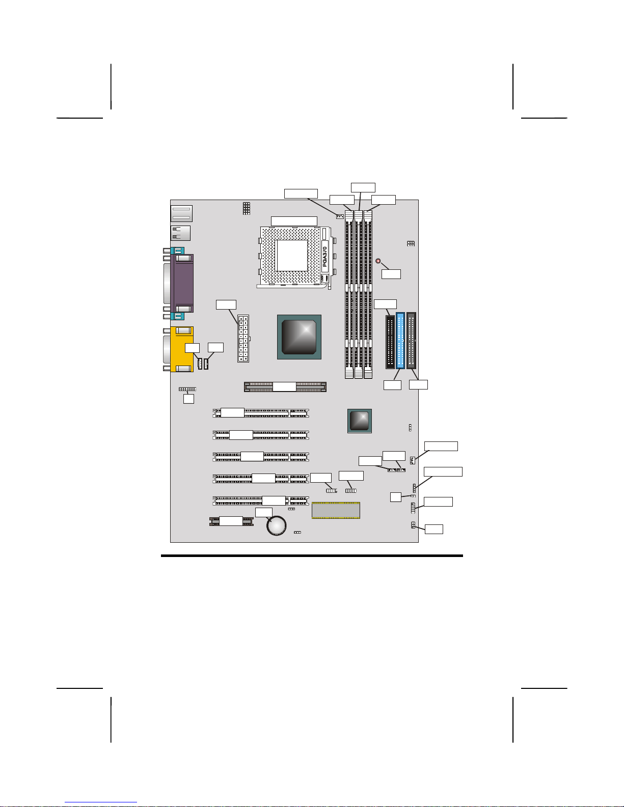
MMaaiinnbbooaarrdd CCoommppoonneenntts
s
CPUFAN
C
A
S
F
A
N
D
M
M
D
M
M
D
M
M
LED
D
E
A
T
X
J1
CD1
AGP
PCI1
PCI2
PCI3
PCI4
PCI5
AMR
BT1
USB
EUSB
JP1
JP9
JP8
JP10
JP12
WOLWOM
S
P
E
A
K
E
R
P
A
N
E
S
R
D
D
J2
CD2
D
E
JP2
JP3
JP4
JP5
JP6
A
GP1
PCI1
PCI2
PCI3
PCI4
PCI5
AMR1
BT1
USB2
EUSB1
WOL1
WOM1
SIR1
PANEL1
SPEAKER1
LED1
IDE1
IDE2
DIMM3
DIMM2
DIMM1
CPU SOCKET
CPUFAN1
ATX1
CD1
CD2
J1
CASFAN1
J2
FDD1
Page 13

7
Table of Mainboard Components
Label Component
AGP1 Accelerated Graphics Port
AMR1 Audio modem riser (AMR) slot
ATX1 Power connector
BT1 Three volt realtime clock battery
CASFAN1 Auxiliary case cooling fan
CD1 Primary CD-in connector
CD2 Secondary CD-in connector
CPU Socket PGA370 CPU Socket
CPUFAN1 Cooling fan for CPU
DIMM1 ~ DIMM3 Three 184-pin DIMM sockets
EUSB1 Connector for front panel USB ports
FDD1 Floppy disk drive connector
IDE 1 Primary IDE channel
IDE 2 Secondary IDE channel
J1 Auxiliary IR/keyboard/mouse header
J2 Sleep switch indicator
LED1 3 VSB for SDRAM (red)
PANEL1 Connector for case front panel switches and LED
indicators
PCI1 ~ PCI5 Five 32-bit add-in card slots
SIR1 Serial infrared cable header
SPEAKER1
Speaker connector
USB2 Front panel USB headers
WOL1 Wake On LAN wakeup connector
WOM1 Wake On Modem wakeup connector
Note:
LED1 is usually connected to a light that indicates that the computer is powered
on. Do not install hardware or disconnect power cables while the LED is on.
Page 14

8
CChhoooossiinngg aa CCoommppuutteerr CCaasse
e
There are many types of computer cases on the market. T he
mainboard complies with the specifications for the ATX system case. Some f eatures on the mainboar d are implem ented
by cabling connectors on the mainboard to indicators and
switches on the s ystem case. Ensure that your case supports
all the features requir ed. The mainboard can s upport two CD
drives, one floppy diskette drive and four enhanced IDE drives.
Ensure that your case has suff icient power and space for all
the drives that you intend to install.
Most cases have a choice of I/O tem plates in the rear panel.
Make sure that the I/O template in the case matches the I/O
ports installed on the rear edge of the mainboard.
This mainboard has an ATX form factor of 220 x 304 mm.
Choose a case that accommodates this form factor.
This concludes Chapter 1. T he next chapter explains how to
install the mainboard.
Page 15

CChhaapptteerr 2
2
Installing the Mainboard
SSaaffeettyy PPrreeccaauuttiioonns
s
Follow these safety precautions when installing the mainboard:
• Wear a grounding strap attached to a grounded device
to avoid damage from static electricity.
• Discharge static electricity by touching the metal case
of a safely grounded object before working on the
mainboard.
• Leave components in the static-proof bags they came
in.
• Hold all circuit boards by the edges. Do not bend cir-
cuit boards.
Page 16

10
QQuuiicckk GGuuiidde
e
This Quick Guide suggests th e steps you can take to as semble your system with the mainboard.
The following table pro vides a reference for installing specific
components:
Locating Mainboard Components
Go to page 6
Setting Jumpers
Go to page 11
Installing the Mainboard in a Case
Go to page 16
Installing Case Components
Go to page 17
Installing the CPU
Go to page 19
Installing Memory
Go to page 22
Installing an HDD and CD-ROM Drive
Go to page 23
Installing an FDD
Go to page 27
Installing Add-on Cards
Go to page 28
Connecting Options
Go to page 30
Connecting Peripheral (I/O) Devices
Go to page 33
Note: The appendix provides a quick reference for jumper
settings.
Page 17
11
CChheecckkiinngg JJuummppeerr SSeettttiinnggs
s
This section explains how to set jumpers for correct configuration of the mainboard.
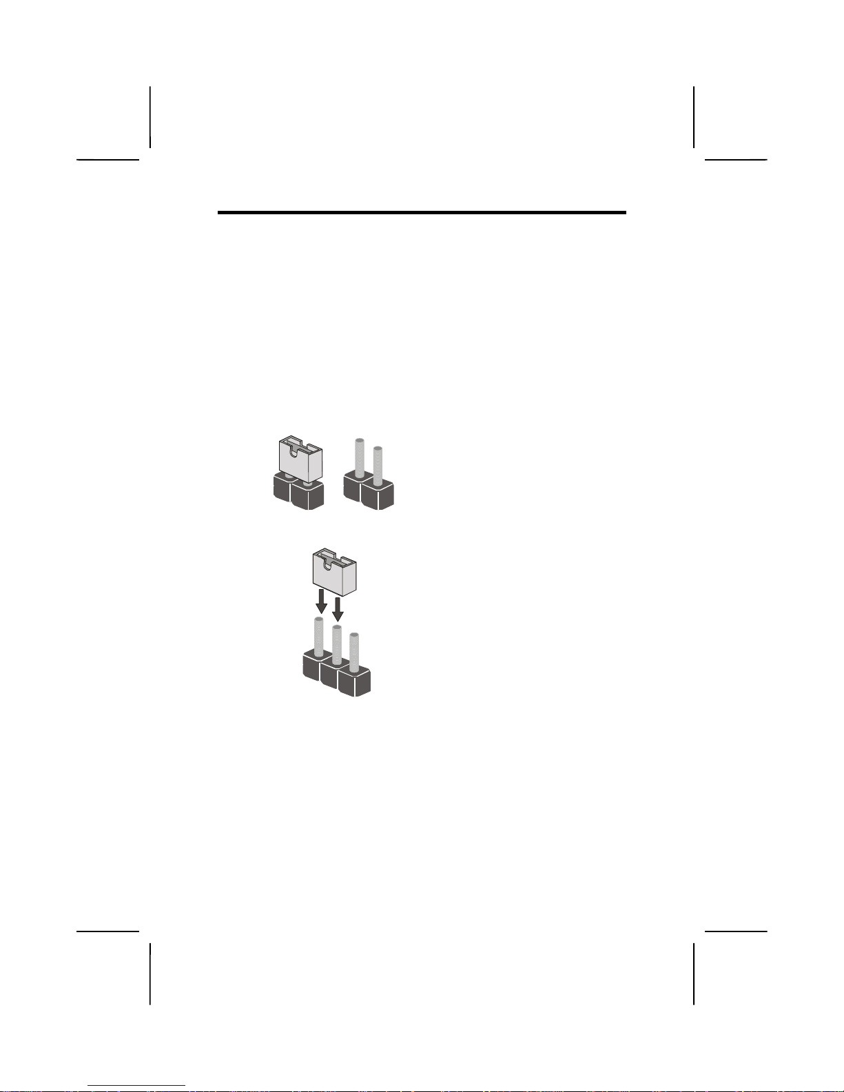
Setting Jumpers
Use the mainboard jumpers to set system configuration options. Jumpers with m ore than one pin are num bered. When
setting the jumpers, ens ure that the jumper caps are p laced
on the correct pins.
Short Open
This illustration shows a 2-pin
jumper. When the jumper cap is
placed on both pins, the jumper is
SHORT. If you remove the jumper
cap, or place the jumper cap on
just one pin, the jumper is OPEN.
1
2
3
This illustration shows a 3-pin
jumper. Pins 1 and 2 are SHORT.
Page 18

12
Checking Jumper Settings
The following illustrat ion shows the location of the mainboard
jumpers. Pin 1 is labeled.
CPUFAN1
CASFAN1
DIMM1
DIMM2
DIMM3
LED1
IDE2
ATX1
J1
CD1
AGP1
PCI1
PCI2
PCI3
PCI4
PCI5
AMR1
BT1
USB2
EUSB1
JP1
JP9
JP8
JP10
JP12
WOL1WOM1
SPEAKER1
PANE L 1
SIR1
FDD1
J2
CD2
IDE1
JP2
JP3
JP4
JP5
JP6
1
1
1
1
1
1111
1111
1111
1111
1111
11111111
1111
1111
1111
1
JP2
JP8
JP6
JP4
JP5
JP3
JP9
JP10
J
P1
1
1
1
1
1
1
1
1
1111
Page 19
13
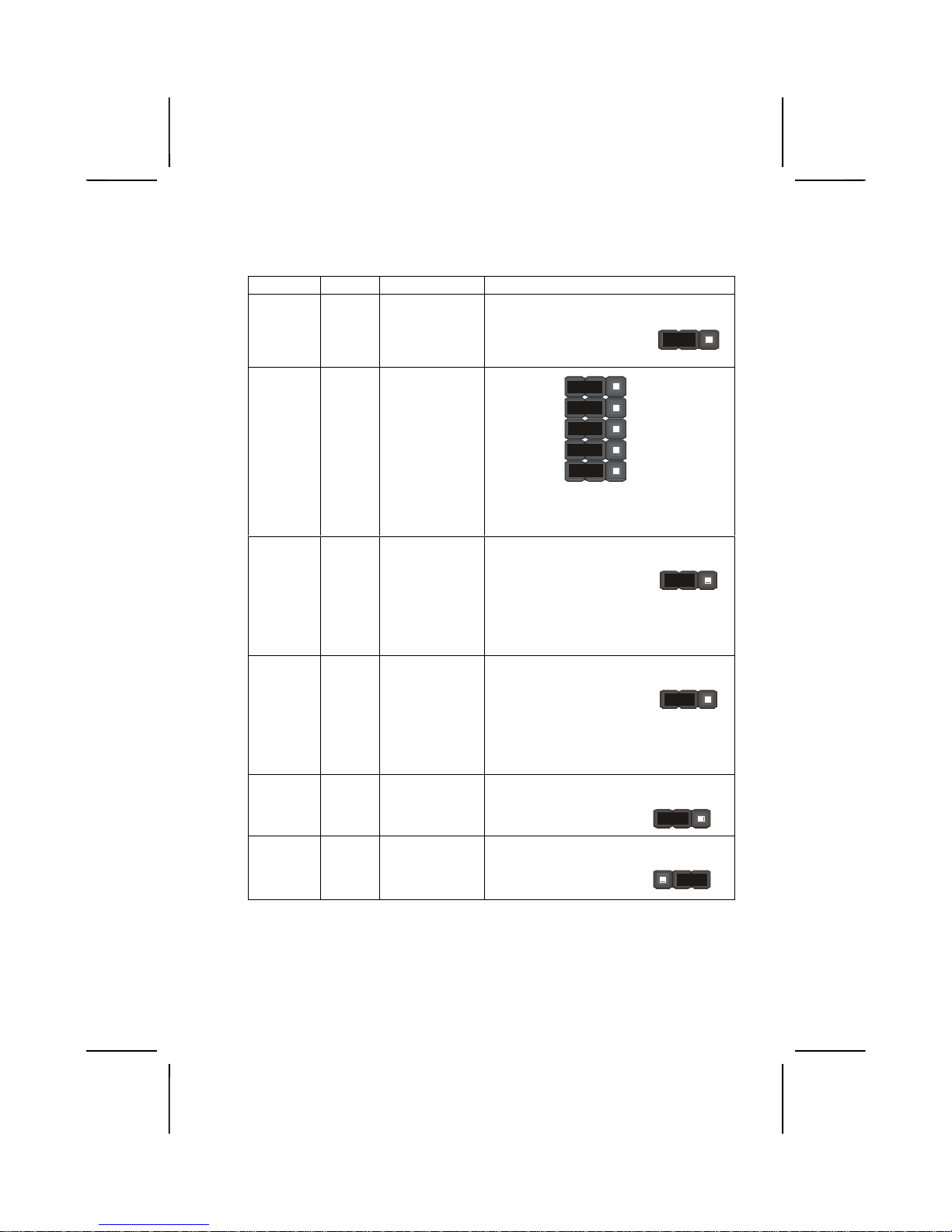
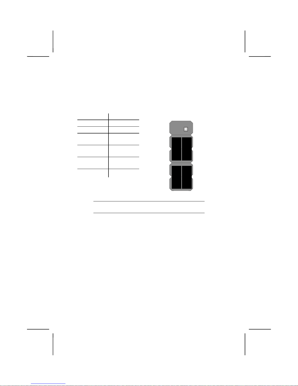
Jumper Settings
Jumper Type Description Setting (
default
)
JP1 3 pin Clear CMOS
jumper
1-2: Normal
2-3: Clear CMOS
JP1
1
JP2
JP3
JP4
JP5
JP6
3 pin CPU core
voltage select
jumper
JP2
JP4
JP5
JP3
1
1
1
1
Refer to the table on page 15 for pin
information.
JP8 3 pin CPU fre-
quency select
jumper
1-2: Normal
operation
2-3: Force a 66
MHz FSB to
run at 100 MHz
FSB
JP8
1
JP9 3 pin CPU fre-
quency
jumper
1-2: Normal
operation
2-3: Force a 100
MHz FSB to
run at 133 MHz
FSB
JP9
1
JP10 3 pin BIOS flash
protection
jumper
1-2: Disable
2-3: Enable
JP10
1
JP12 3 pin AC resume
jumper
1-2: Enable
2-3: Disable
JP12
1
Page 20

14
JP1: Clear CMOS Jumper
This jumper enables you to reset BIOS:
1. Turn the system off.
2. Short pins 2 and 3 on jumper 1.
3. Return the jumper to the normal setting.
4. Turn the system on. The BIOS is returned to the default settings.
JP2-JP6: CPU Frequency Selection
Refer to the table on page 15.
JP8: CPU Frequency Select Jumper 1
This jumper is used to forc e the CPU clock to run at a higher
frequency than it is r ated. It is recom mend that you leave the
jumper on the normal setti ng. See table abov e for more inf ormation
JP9: CPU Frequency Select Jumper 2
This jumper is used to forc e the CPU clock to run at a higher
frequency than it is r ated. It is recom mend that you leave the
jumper on the normal setti ng. See table abov e for more inf ormation.
Note: The CPU speed is determined by the CPU Host/PCI
Clock speed multiplied by the CPU Clock Ratio.
Refer to the Frequency Control Option in Chapter 3
for more information. Also, note that Forcing the
CPU to run at a higher clock speed then it was rated
for is called overclocking and is not recommended.
JP10: BIOS Flash Protect Jumper
This jumper is used to protect t he BIOS from being unintentionally flashed. Enab le this jumper for protec tion and disable
this jumper when you want to flash the BIOS.
JP12: AC Resume Jumper
Use this jumper to set the power state after an unexpected
shutdown due to AC power interruption.
Page 21

15
Jumper 2 – 6 pin settings
Pin Settings
V olt. JP6 JP5 JP4 JP3 JP2
Auto* 1-2 1-2 1-2 1-2 1-2
1.050V 2-3 2-3 Open 2-3 2-3
1.075V 2-3 2-3 Open 2-3 Open
1.100V Open Open 2-3 2-3 2-3
1.125V Open Open 2-3 2-3 Open
1.150V 2-3 Open 2-3 2-3 2-3
1.175V 2-3 Open 2-3 2-3 Open
1.200V Open 2-3 2-3 2-3 2-3
1.225V Open 2-3 2-3 2-3 Open
1.250V 2-3 2-3 2-3 2-3 2-3
1.275V 2-3 2-3 2-3 2-3 Open
1.300V Open Open Open Open 2-3
1.325V Open Open Open Open Open
1.350V 2-3 Open Open Open 2-3
1.375V 2-3 Open Open Open Open
1.400V Open 2-3 Open Open 2-3
1.425V Open 2-3 Open Open Open
1.450V 2-3 2-3 Open Open 2-3
1.475V 2-3 2-3 Open Open Open
1.500V Open Open 2-3 Open 2-3
1.525V Open Open 2-3 Open Open
1.550V 2-3 Open 2-3 Open 2-3
1.575V 2-3 Open 2-3 Open Open
1.600V Open 2-3 2-3 Open 2-3
1.625V Open 2-3 2-3 Open Open
1.650V 2-3 2-3 2-3 Open 2-3
1.675V 2-3 2-3 2-3 Open Open
1.700V Open Open Open 2-3 2-3
1.725V Open Open Open 2-3 Open
1.750V 2-3 Open Open 2-3 2-3
1.775V 2-3 Open Open 2-3 Open
1.800V Open 2-3 Open 2-3 2-3
1.825V Open 2-3 Open 2-3 Open
*Auto: When all 1-2 pins are shorted, the core voltage will automatically be determined.
Note: These values are for reference only. It is not recommend-
ed to change the settings for jumper 2 ~ 6. Please notice
that the CPU will burn out if the core voltage is higher
than the default value.
Page 22
16
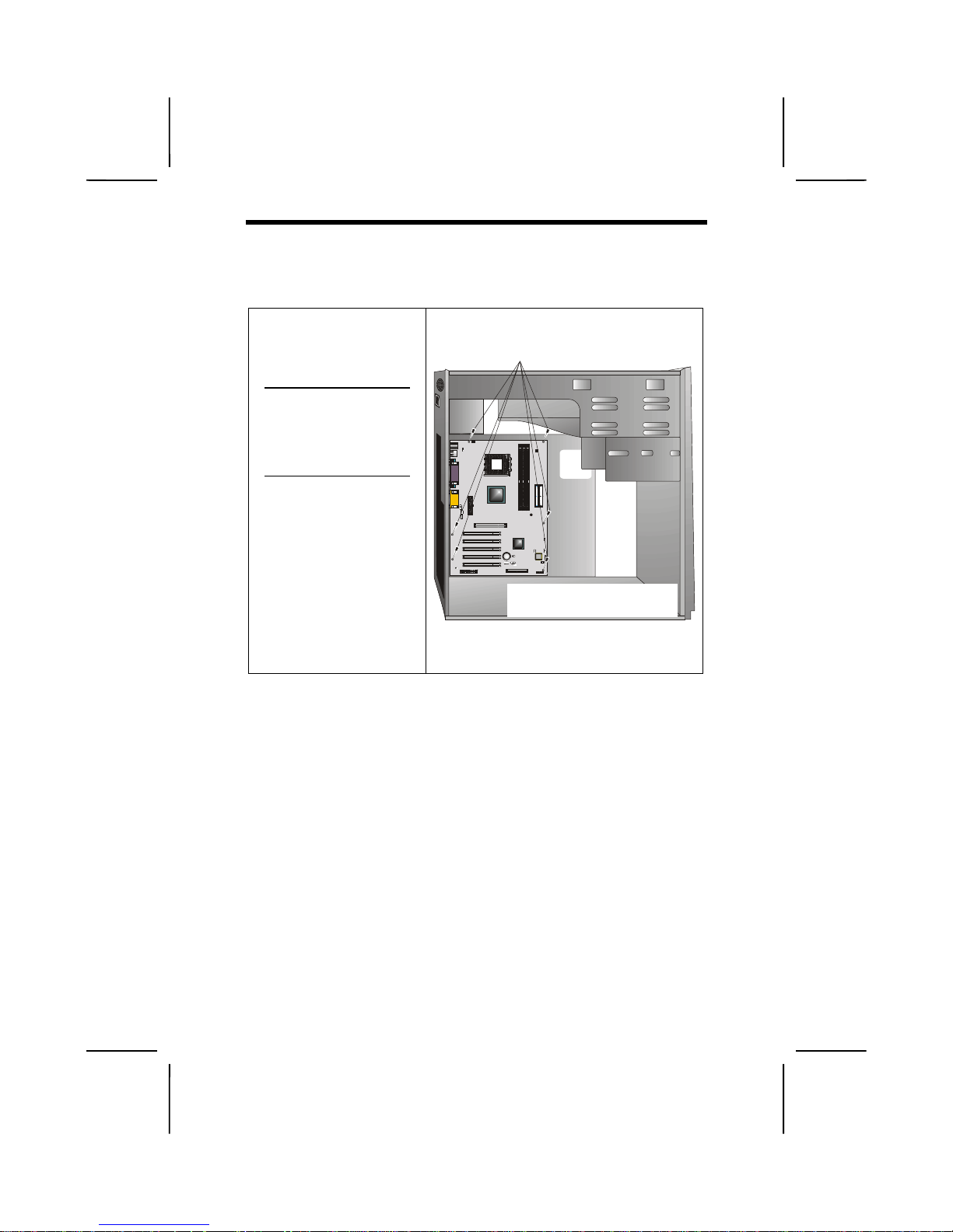
IInnssttaalllliinngg tthhee MMaaiinnbbooaarrdd iinn aa CCaasse
e
Refer to the following illus tration and instructions for installing
the mainboard in a case:
This illustration shows
an example of a mainboard being installed in
a tower-type case:
Note: Do not over-
tighten the
screws as this
can stress the
mainboard.
Most system cases have
mounting brackets installed in the case,
which correspond to the
holes in the mainboard.
Place the mainboard
over the mounting
brackets and secure the
mainboard onto the
mounting brackets with
screws.
2. S
ecure the mainboard with
screws where appropriate.
1. Place the mainboard
over the mounting brackets.
Ensure that your c ase has an I/O template t hat supports the
I/O ports and expansion slots on your mainboard.
Page 23
17
CCoonnnneeccttiinngg CCaassee CCoommppoonneenntts
s
After you have installed the m ainboard into a case, you can
begin connecting the mainboard components. Refer to the
following:
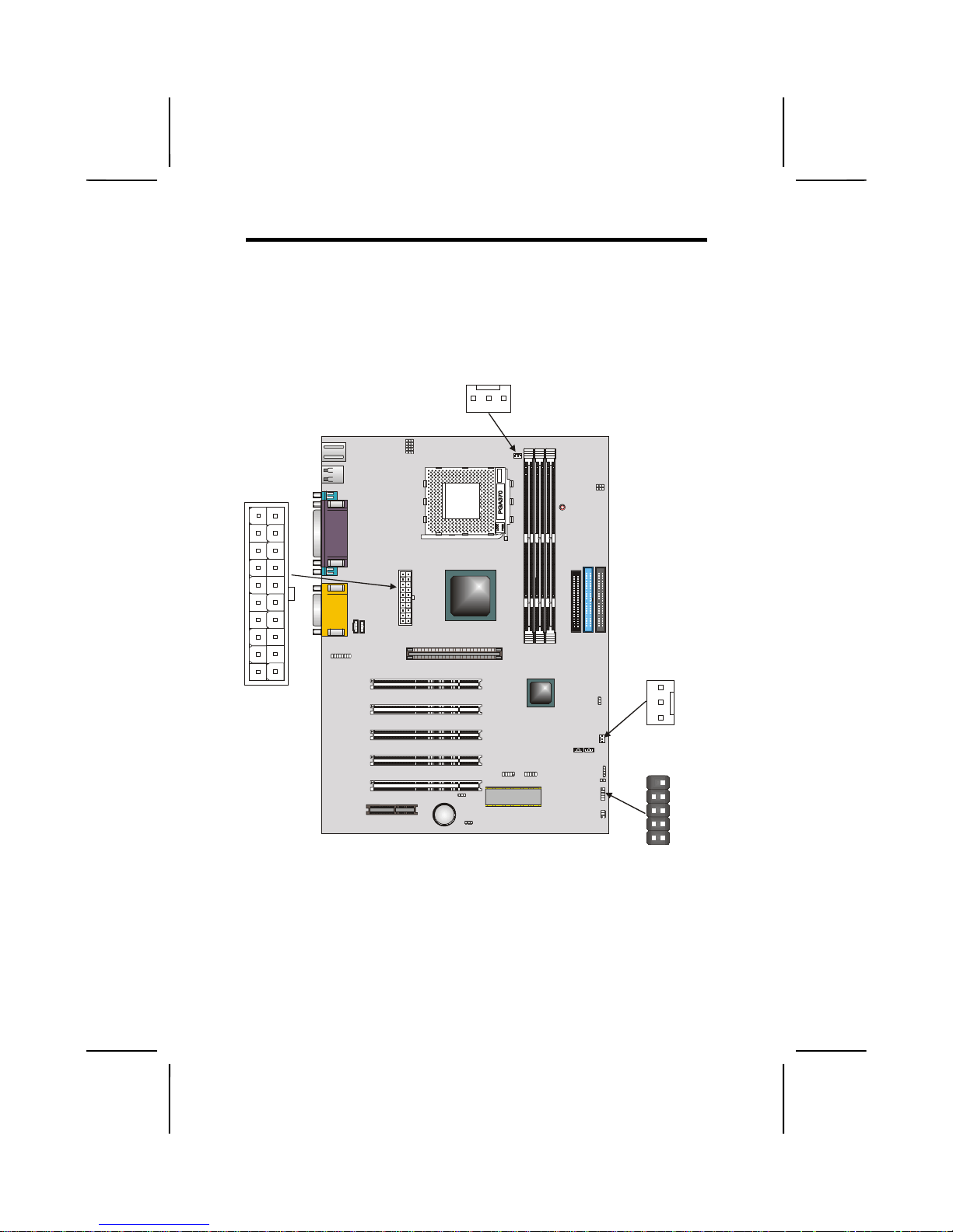
5. Connect the case power supply connector to ATX1.
6. Connect the CPU cooling fan cable to CPUFAN1.
7. Connect the case cooling fan connector to CASFAN1
The following page explains how to make PANEL1 connections.
CPUFAN1
CASFAN1
DIMM1
DIMM2
DIMM3
LED1
IDE2
ATX1
J1
CD1
AGP1
PCI1
PCI2
PCI3
PCI4
PCI5
AMR1
BT1
USB2
EUSB1
JP1
JP9
JP8
JP10
JP12
WOL1WOM1
SPEAKER1
PANEL1
SIR1
FDD1
J2
CD2
IDE1
JP2
JP3
JP4
JP5
JP6
1
1
1
1
1
1111
1111
1111
1111
1111
11111111 1111
1111
1111
1
C
PUFAN1
CASFAN1
ATX1
PANEL1
1
1
Page 24
18
The Panel Connector
The panel connector provides a standard set of switch and
LED connectors commonly found on ATX or micro-ATX cases.
Refer to the table below for information:
Device Pins
Empty 10
N/C 9
Power
ON/OFF
6, 8
Reset
Switch
5, 7
Green LED
Indicator
+2, -4
HDD LED +1, -3
HDD LED
(Pins 1, 3)
2 1
Reset Switc
h
(Pins 5, 7)
Power Switch
(Pins 6, 8)
Green LED
(Pins 2, 4)
Empty
(Pin 10)
10 9
N/C
(Pin 9)
Note: The plus sign (+) indicates a pin which mu st be con-
nected to a positive voltage.
Page 25

19
IInnssttaalllliinngg HHaarrddwwaarre
e
Installing the Processor
Caution:
When installing a CPU heatsink and cooling fan
make sure that you DO NOT scratch the mainboard or any
of the surface-mount resistors with the clip of the cooling
fan. If the clip of the cooling fan scrapes across the mainboard, you may cause serious damage to the mainboard or
its components.
On most mainboards, there are small surface-mount resistors near the processor socket, which may be damaged if
the cooling fan is carelessly installed.
Avoid using cooling fans with sharp edges on the fan casing
and the clips. Also, install the cooling fan in a well-lit work
area so that you can clearly see the mainboard and processor socket.
Before installing the Processor
This mainboard autom atically determines the CPU clock frequency and system bus frequenc y for the process or. You m ay
be able to change these s ettings by making changes t o jumpers on the mainboar d, or ch angin g the s ettings in t he syst em
Setup Utility. We strongly recommend that you do not overclock processors or other components to run f aster than their
rated speed.
Warning:
Overclocking components can adversely affect
the reliability of the system and introduce errors into your
system. Overclocking can permanently damage the mainboard by generating excess heat in components that are
run beyond the rated limits.
This mainboard has a Socket 370 processor socket. When
choosing a processor, consider the p erform anc e requirem ents
of the system. Perf ormance is based on the processor desi gn,
the clock speed and system bus frequency of the processor,
and the quantity of intern al c ach e m emor y and ext erna l c ache
memory.
Page 26

20
CPU Installation Procedure
The following illustration shows CPU installation components:
Note: The pin-1 corner on the CPU and socket is empty.
Locking lever
Pin-1 corner
CPU fan
Socket 370
Page 27

21
Follow these instructions to install the CPU:
1. Pull the CPU socket locking lever away from the socket to unhook it and raise the locking lever to the upright
position.
2. Match the pin A-1 corner on the CPU socket and the
pin A-1 corner on the processor and insert the proces sor into the socket. Do not use force.
3. Match the pin A-1 corners and insert the processor into
the socket. Do not use force.
4. Swing the locking lever down and hook it under the
latch on the edge of the socket.
5. Plug the CPU fan power cable into the CPU cooling
fan power supply on the mainboard (CPUFAN1).
Note: After you have assembled the system, you must set
the correct clock speed and frontside bus (FSB)
speed. Check the jumper section in Appendix A if
your mainboard has jumpers that control the FSB,
and refer to Frequency Vol t age Control on page 63
for more information.
Locking lever
CPUFAN1
CPU fan connector
CPU fan and
heatsink assembly
Pin-1 corners
Page 28

22
Installing Memory Modules
For this mainboard, you must use 168-pin 3.3V non- buffered
Dual In-line Memory Modules (DIMMs). The memory chips
must be standard or registered SDRAM and VCM SDRAM
memory chips.
The memory bus can run at 66 MH z, 100 MHz, or 133 MH z. If
your processor operates o ver a 133 MHz system bus, you ca n
install PC133 or PC100 m emory that operates over a 133 or
100 MHz bus. If your processor operates over a 100 MHz
system bus, you can install memory that operates over a
133MHz, 100 MHz or 66 MHz bus. If your proc essor operates
over a 66MHz, you can o nly i nsta ll m em ory chips that oper ate
at 66MHz or 100MHz.
Memory Configurations
The table below displays supported memory configurations:
Technology
(Mbit)
Configuration # of Row
Addrs Bits
# of Col
Addrs Bits
# of Bank
Addrs Bits
Page Size
(Kb)
64 8M x 8 12 8 2 4
64 4M x 16 12 9 2 2
128 32M x 4 12 11 2 16
128 16M x 8 12 10 2 8
Note: 32M x 4 128 Mbit is for registered DIMMs only, 4M x
16 64 Mbit support is for unbuffered DIMMs only.
The table below displays maximum memory for DIMMs.
1 DIMM 2 DIMMs 3 DIMMsDRAM
Configuration
SS
(MB)DS(MB)SS(MB)DS(MB)SS(MB)
DS
(MB
64 Mbit 8M x 8 64 128 128 256 192 384
64 Mbit 4M x 16 32 64 64 128 96 192
128 Mbit 16M x 8 128 256 256 512 384 768
128 Mbit 32M x 4 256 512 512 1024 768 1536
Note: SS = Single Sided
DS = Double Sided
Page 29

23
Installation Procedure
The mainboard accommodates three memory modules. You
must install at leas t on e module in any of the thr ee s lots. Each
module can be installed with 32 MB to 512 MB of m emory;
total memory capacity is 1.5 GB.
Refer to the following to install the memory modules.
1. Push the latches on each side of the DIMM slot down.
2. Align the memory module with the slot. The DIMM
slots are keyed with notches and the DIMMs are keyed
with cutouts so that they can only be installed correctly.
3. Check that the cutouts on the DIMM module edge
connector match the notches in the DIMM slot:
Cutouts
Notches
Latch
4. Install the DIMM module into the slot and press it firmly
down until it seats correctly. The slot latches are levered upwards and latch on to the edges of the DIMM.
5. Install any remaining DIMM modules.
Page 30

24
Installing a Hard Disk Drive/CD-ROM
This section describes how to install IDE devices such as a
hard disk drive and a CD-ROM drive.
About IDE Devices
Your mainboard has a primary and secondary IDE channel interface (IDE1 and IDE2) . An IDE ribbon cabl e supportin g two IDE
devices is bundled w ith t he mai nboa rd.
If you want to install m or e than two IDE de vices, g et a sec ond
IDE cable and you can add two more devices to the s econdary IDE channel.
IDE devices have jumpers or switches tha t are used to s et the
IDE device as MASTER or SLAVE. Refer to the IDE device
user’s manual. When ins talling two IDE d evices on one cab le,
ensure that one device is s et to MASTER and the other device is set to S LAVE. The documentation of your ID E device
explains how to do this.
About UltraDMA
This mainboard suppor ts Ultra DMA 66/ 100. UDMA is a t echnology that accelerates the p erform ance of dev ices in the IDE
channel. Install IDE d evices that support UDMA and use IDE
cables that support UDMA for better performance.
Page 31

25
Installing a Hard Disk Drive
1. Install the hard disk drive into the drive cage in your
ATX system case.
2. Plug the IDE cable into IDE1.
A
B
C
HDD
Pin 1
Note: Ribbon cable connectors are usually keyed so that
they can only be installed correctly on the device
connector. If the connector is not keyed, make sure
that you match the pin-1 side of the cable connector
with the pin-1 side of the device connector. Each
connector has the pin-1 side clearly marked. The
pin-1 side of each ribbon cable is always marked
with a colored stripe on the cable.
3. Plug an IDE cable connector into the hard disk drive
IDE connector. It doesn't matter which connector on
the cable you use. Ensure that the pin-1 side of the
cable is matched with the pin-1 side of the connector.
Refer to the previous note.
4. Plug a power cable from the case power supply into
the power connector on the hard disk drive.
When first starting up your system, the BIOS should automatically detect your hard disk drive. If it doesn’t, enter Setup
Utility and use IDE Hard Disk Auto Detect feature to configure
the hard disk drive that you have installed. See IDE HDD
Auto-Detection on page 40 for more information.
Page 32

26
Installing a CD-ROM/DVD Drive
1. Install the CD-ROM/DVD drive into the drive cage in
your ATX system case.
2. Plug the IDE cable into IDE1 (A). If you have already
installed an HDD, use the other connector on the IDE
cable.
A
Pin 1
CD-ROM
B
C
CD-ROM audio
connector
CD2
CD1
D
Note: Ribbon cable connectors are usually keyed so that
they can only be installed correctly on the device
connector. If the connector is not keyed, make sure
that you match the pin-1 side of the cable connector
with the pin-1 side of the device connector. Each
connector has the pin-1 side clearly marked. The
pin-1 side of each ribbon cable is always marked
with a colored stripe on the cable.
3. Plug an IDE cable connector into the CD-ROM/DVD
drive IDE connector. It doesn't matter which connector
on the cable you use. Ensure that the pin-1 side of the
cable is matched with the pin-1 side of the connector.
Refer to the previous note.
Page 33

27
4. Use the audio cable provided with the CD-ROM/DVD
drive to connect to the mainboard CD-in connector
CD1 or CD2.
5. Plug a power cable from the case power supply into
the power connector on the CD-ROM/DVD drive.
When you first start up your system, the BIOS should automatically detect your CD-ROM/ DVD drive. If it doesn’t, enter
the Setup Utility and configure the CD-ROM/DVD drive that
you have installed. See IDE Prim ary/Secondary Mast er/Slave
(Auto) on page 40 for more information.
Installing a Floppy Diskette Drive
The mainboard has a floppy diskette drive (FDD) interface
and ships with a diskette dr ive ribbon cable that s upports o ne
or two floppy diskette drives. You can install a 5.25-inch drive
and a 3.5-inch drive with various cap acities. The floppy diskette drive cable has one type of connector for a 5.25-inch
drive and another type of connector for a 3.5-inch drive.
1. Install the FDD into the drive cage in your ATX system
case.
2. Plug the FDD cable into FDD1.
FDD
B
C
A
Pin 1
Page 34

28
Note: Ribbon cable connectors are usually keyed so that
they can only be installed correctly on the device
connector. If the connector is not keyed, make sure
that you match the pin-1 side of the cable connector
with the pin-1 side of the device connector. Each
connector has the pin-1 side clearly marked. The
pin-1 side of each ribbon cable is always marked
with a colored stripe on the cable.
3. Plug the correct connector on the FDD cable for the
5.25-inch or 3.5-inch drive into the FDD connector (B).
4. Plug a power cable from the case power supply into
the power connector on the FDD.
When you first start up your system, go immediately to the
Setup Utility to configure the floppy diskette drives that you
have installed. See Standard CMOS Features on page 39 for
more information.
Installing Add-on Cards
This mainboard has five 32-bit PCI (Peripheral Components
Interconnect) expansion slots, and one 4xAGP slot.
4xAGP Slot
The 4xAGP slot is used to install a graphics
adapter that supports the 4xAGP specification and has a 4xAGP edge connector.
PCI Slots
PCI slots are used to install expansion cards
that have the 32-bit PCI interface.
AMR
The Audio Modem Riser slot can be used to
insert an AMR card.
Note: Before installing an add-in card, check the docu-
mentation for the card carefully. If the card is not
Plug and Play, you ma y have to ma nua lly configure
the card before installation.
Page 35

29
1. Remove a blanking plate from the system case corresponding to the slot you are going to use.
2. Install the edge connector of the add-in card into the
expansion slot. Ensure that the edge connector is correctly seated in the slot.
Edge connector
Add-on card
3. Secure the metal bracket of the card to the system
case with a screw.
Note: For some add-in cards, for example graphics adap-
ters and netwo rk adapters, you have to i nstall
drivers and software before you can begin using t he
add-in card.
CASFAN1
DIMM1
DIMM2
DIMM3
IDE2
J1
CD1
AGP1
PCI1
PCI2
PCI3
PCI4
PCI5
AMR1
BT1
USB2
EUSB1
JP1
JP10
JP12
WOL1WOM1
SPEAKER1
PANEL1
SIR1
FDD
1
J2
CD2
IDE1
1111
1111
1111
11111111
1111
1111
1111
1
AGP
PCI
AMR
Page 36

30
Connecting Optional Devices
Refer to the following for info rmation on connectin g the mainboard’s optional devices :
CASFAN1
DIMM1
DIMM2
DIMM3
IDE2
J1
CD1
AGP1
PCI1
PCI2
PCI3
PCI4
PCI5
AMR1
BT1
USB2
EUSB1
JP1
JP10
JP12
WOL1WOM1
SPEAKER1
PANEL1
SIR1
FD
J2
CD2
IDE1
1111
1111
1111
1111
11111
11
1
1111
1111
1
J1
USB2
EUSB1
WOL1
WOM1
J2
SIR1
SPEAKER1
1111
1111
1111
1111
1111
J1: Auxiliary IR/keyboard/mouse header
This header allows the user to install auxiliary front-oriented
microphone and line-out ports for easier access.
Pin Signal Name Pin Signal Name
1
3
5
7
9
11
13
15
LINEOUT (R)
AGND
GND
+12V
MIC
Front LINE Out (R)
Front LINE Out (L)
GND
2
4
6
8
10
12
14
16
LINEOUT (L)
AGND
GND
NC
GND (MIC)
LINE NEXT (R)
LINE NEXT (L)
NC
USB2: USB port
The mainboard has t wo USB ports i nstalled on the rear edge
I/O port array. Some computer cases have a spec ial module
that mounts USB ports at the front of the case. If you have this
kind of case, use auxiliary US B connectors USB2 and USB3
to connect the front-mounted ports to the mainboard.
Page 37

31
Pin Signal Name Pin Signal Name
1
3
5
7
9
VREG_FP_USBPWR0
USB_FP_P0USB_FP_P0+
Ground
Key
2
4
6
8
10
VREG_FP_USBPWR0
USB_FP_P1USB_FP_P1+
Ground
USB_FP-OC0
EUSB1: USB port
The mainboard has a USB p ort installed on the rear edge I/O
port array. Some computer cases have a specia l module that
mounts USB ports at the front of the case. If you have this
kind of case, use auxi liary USB c onnectors on EUSB 1 to connect the front-mounted ports to the mainboard.
Pin Signal Name Pin Signal Name
1
3
5
7
9
USBVCC
-DATA1
+DATA1
GND
GND
2
4
6
8
10
GND
GND
+DATA3
-DATA3
USBVCC
WOL1/WOM: Wake On LAN/Wake On Modem
If you have installed a LAN card, use the c able provided with
the card to plug into t he m ainboar d W OL1 c onnector. This enables the Wake On LAN (WOL) feature. W hen your s ystem is
in a power-saving mode, any LAN signal automatically resumes the system. You must enable this item using the Power
Management page of the Setup Utility.
Pin Signal Name
1
2
3
5VSB
Ground
SENSE
If you have installed a modem, use the cable provided with
the modem to plug into th e mainboar d WO M1 connector. This
enables the Wake On Modem (WOM) feature. When your
system is in a power-saving mode, an y modem signal au tomatically resumes the system. You must enable this item
using the Power Managem ent page of the Setup Utility. See
Chapter 3 for more information.
Page 38

32
SIR1: Serial infrared port
The mainboard supports a Seria l Infrared (SIR) data port. Infrared ports allow the wireless exchange of information
between your com puter and similarly equipped d evices such
as printers, laptops, Personal Digital Assistants (P DAs), and
other computers.
Pin Signal Name
1
2
3
4
5
6
Not assigned
(No Pin)
+5V
Ground
IRTX
IRRX
J2: Sleep switch
This connector attaches to a front pane l button used to l eave
the system in a sleep state.
Pin Signal Name
12Positive
Negative
SPEAKER1: Internal speaker
Connect the internal speaker connector to this header.
Pin Signal Name
1
2
3
4
SPKR
NC
Ground
+5V
Page 39

33
CCoonnnneeccttiinngg II//OO DDeevviiccees
s
The backplane of the mainboard has the following I/O ports:
PS/2
mouse
PS/2
keyboard
USB
ports
Pa ra lle l p ort (LPT 1)
Serial port
COM 1
Serial port
COM 2
Line-in
Game port
Microphone
Line-out
PS/2 Mouse
Use the upper PS/2 port to connect a
PS/2 pointing device.
PS/2 Keyboard
Use the lower PS/2 port to connect a
PS/2 keyboard.
USB Ports
Use the USB ports to connect USB
devices.
LPT1
Use LPT1 to connect printers or other
parallel communications devices.
COM1/2
Use the COM ports to connect serial
devices such as mice or fax/modems.
COM1 is identified by the system as
COM1/3. COM2 is identified by the
system as COM2/4.
Game Port
Use the game port to connect a joystick or a MIDI device.
Audio Ports
Use the three audio ports to connect
audio devices. The left side jack is for
a stereo line-out signal. The middle
jack is for a stereo line-in signal. The
right side jack is for a microphone.
Page 40

34
External Connector Color Coding
Many connectors now use standard colors as shown in the
table below.
Connector Color
Analog VGA Blue
Audio line-in Light blue
Audio line-out Lime
Digital monitor/flat panel White
IEEE 1394 Grey
Microphone Pink
MIDI/Game Gold
Parallel Burgundy
PS/2-compatible keyboard Purple
PS/2-compatible mouse Green
Serial Teal or Turquoise
Speaker out/subwoofer Orange
Right-to-left speaker Brown
USB Black
Video out Yellow
SCSI, network, telephone,
modem
None
This concludes Chapter 2. The next chapter covers the BIOS.
Page 41

CChhaapptteerr 3
3
Using BIOS
AAbboouutt tthhee SSeettuupp UUttiilliitty
y
The computer uses the latest Award BIOS with support for
Windows Plug and Play. The CMOS chip on the mainboard
contains the ROM setup instructions f or configuring th e mainboard BIOS.
The BIOS (Basic Input and Output System) Setup Utili ty displays the system's configuration status and provides you with
options to set system par ameters. T he parameters are st ored
in battery-backed-up CMOS RAM that saves this inform ation
when the power is turned off. When the s ystem is turned back
on, the system is configured with the values you stored in
CMOS.
The BIOS Setup Utility enables you to configure:
• Hard drives, diskette drives, and peripherals
• Video display type and display options
• Password protection from unauthorized use
• Power management features
The settings made in the Se tup Uti lit y aff ec t how the c omputer
performs. Before us ing the Setup Utility, ensure that you understand the Setup Utility options.
This chapter provides explanations for Setup Utility options.
Page 42

36
The Standard Configurat ion
A standard configuration has already been set in the Setup
Utility. However, we recommend that you read this chapt er in
case you need to make any changes in the future.
This Setup Utility should be used:
• when changing the system configuration
• when a configuration error is detected and you are
prompted to make changes to the Setup Utility
• when trying to resolve IRQ conflicts
• when making changes to the Power Management con-
figuration
• when changing the password or making other changes
to the Security Setup
Page 43

37
Entering the Setup Utility
When you power on the system , BIOS enters the Power-On
Self Test (POST) r outines. POST is a series of bui lt-in diagnostics perform ed by the BIOS. After the POST routines are
completed, the following message appears:
Press DEL to enter SETUP
Pressing the delete ke y accesses the Award BIOS Setup
Utility:
CMOS Setup Utility – Copyright (C) 1984 – 2001 Award Software
Standard CMOS Features
Advanced BIOS Features
Advanced Chipset Features
Integrated P eripherals
Power Management Setup
PnP/PCI Configurations
PC Health Status
Frequency/Voltage Control
Load Fail-Safe Def aul ts
Load Optimized Defa ult s
Set Supervisor Password
Set User Password
Save & Exit Set up
Exit Without Sa ving
Esc : Quit ↑↑↑↑ ↓↓↓↓ →→→→ ←←←← : Select Item
F10 : Save & Exit Setup
Time, Date, Hard Disk Type . . .
BIOS Navigation Keys
The BIOS navigation keys are listed below:
Key Function
Esc Exits the current menu
←↑↓→
Scrolls through the items on a menu
+/–
/PU/PD
Modifies the selected field's values
F10 Saves the current configuration and exits setup
F1
Displays a screen that describes all key func-
tions
F5 Loads previously saved values to CMOS
F6 Loads a minimum configuration for trouble-
shooting.
F7 Loads an optimum set of values for peak per-
formance
Page 44

38
Updating the BIOS
You can download and install updated BIOS for this mainboard from the manufactur er's Web site. New BIOS provides
support for new peripher als, im provem ents in perf orm ance, or
fixes for known bugs. Install new BIOS as follows:
1. If your mainboard has a BIOS protection jumper,
change the setting to allow BIOS flashing. (Refer to
Appendix A for jumper settings.)
2. If your mainboard has an item called Firmware Write
Protect in Advanced BIOS features, disable it. (Firmware
Write Protect prevents BIOS from being overwritten.)
3. Create a bootable system disk. (Refer to Windows online help for information on creating a bootable system
disk.)
4. Download the Flash Utility and new BIOS file from the
manufacturer's Web site. Copy these files to the system diskette you created in Step 3.
5. Turn off your computer and insert the system diskett e in
your computer's diskette drive. (You might need to run
the Setup Utility and change the boot priority items on the
Advanced BIOS Fe atu re s S etu p pag e, to fo rce y ou r
computer to boot fro m the floppy diskette drive fi rst.)
6. At the A:\ prompt, type the Flash Utility program name
and press <Enter>. You see a screen similar to the
following:
FLASH MEMORY WRITER V7.33
(C) Award Software 1999 All Rights Reserved
For (MAINBOARD NAME) DATE: 10/26/2000
Flash Type
File Name to Program :____________________
Error Message
7. Type the filename of the new BIOS in the “File Name
to Program” text box. Follow the onscreen directions to
update the mainboard BIOS.
8. When the installation is complete, remove the floppy
diskette from the diskette drive and restart your computer. If your mainboard has a Flash BIOS jumper,
reset the jumper to protect the newly installed BIOS
from being overwritten.
Page 45

39
UUssiinngg BBIIOOS
S
When you start the Setup Uti lity, the main menu appears. The
main menu of the Setup Utility displays a list of the options
that are available. A highlight indicates which option is currently selected. Use the cursor arrow keys to move the
highlight to other opt ions. When an option is highlighte d, execute the option by pressing <Enter>.
Some options lead to pop-up dialog boxes tha t prompt you to
verify that you wish to exec ute that opt ion. Oth er options lead
to dialog boxes that prompt you for information.
Some options (mark ed with a triangle
) lead to submenus
that enable you to change the values for the option. Use the
cursor arrow keys to scroll through the items in the submenu.
In this manual, default values are enclosed in parenthesis.
Submenu items are denoted by a triangle
.
Standard CMOS Features
This option displays basic information about your system.
CMOS Setup Utility – Copyright (C) 1984 – 2001 Award Software
Standard CMOS Features
Item Help
Date (mm:dd:yy) Tue, July 11 2000
Time (hh:mm:ss) 12 : 8 : 59
IDE Primary Master
IDE Primary Slave
IDE Secondary Master
IDE Secondary Slave
Drive A [1.44M, 3.5 in. ]
Drive B [None]
Floppy 3 Mode Support [Disabled]
Video [EGA/VGA]
Halt On [All,But Keyboard]
Base Memory 640K
Extended Memory 31744K
Total Memory 32768K
Menu Level
Change the day, month,
year and century.
↑↑↑↑ ↓↓↓↓ →→→→ ←←←←
: Move Enter : Select +/-/PU/PD:Value: F10: Save ESC: Exit F1:General Help
F59:Previous Values F6:Fail-Safe Defaults F7:Opti m ized Defaults
Page 46

40
Date and Time
The Date and Time items show the current date a nd time on
the computer. If you are running a Windows OS, these items
are automaticall y updated wh enever you mak e c hanges to t he
Windows Date and Time Properties utility.
IDE Devices (None)
Your computer has two IDE channels (Primary and Secondary)
and each channel can be installed with one or two devices
(Master and Slave). Use these it ems to c onfigure each d evice
on the IDE channel.
Press <Enter> to display the IDE submenu:
CMOS Setup Utility – Copyright © 1984 – 2000 Award Software
IDE Primary Master
Item Help
IDE HDD Auto-D etection Press Enter
IDE Primary Master [Auto]
Access Mode [Auto]
Capacity 0 MB
Cylinder 0
Head 0
Precomp 0
Landing Zone 0
Sector 0
Menu Level
To auto-detect the
HDD’s size, head . . . on
this channel
↑↑↑↑ ↓↓↓↓ →→→→ ←←←←
: Move Enter : Select +/-/PU/PD:Value: F10: Save ESC: Exit F1:General Help
F5:Previous Values F6:Fail-Safe Defaults F7:Optimized Defaults
IDE HDD Auto-Detection
Press <Enter> wh ile th is it em is high lighte d to pr om pt the Setup Utility to automaticall y detect and configure an ID E device
on the IDE channel.
Note: If you are setting up a new har d disk drive t hat sup-
ports LBA mode, more than one line will appear in
the parameter box. Choose the line that lists LBA
for an LBA drive.
IDE Primary/Secondary Master/Slave (Auto)
Leave this item at Auto to enable the system to automatically
detect and c onf ig ure ID E d evi c es on th e ch ann el. If it fa ils to f ind
a device, change the value to Manual and then manually configure the drive by entering the characteristics of the drive in the
items described below .
Page 47

41
Refer to your dr i ve's doc um entat ion or look on th e dr i ve cas ing if
you need to obtain this information. If no device is installed,
change the value to None.
Note: Before attempting to configure a hard disk drive,
ensure that you have the configuration informa tion
supplied by the manufacturer of your hard drive. Incorrect settings can result in your system not
recognizing the installed hard disk.
Access Mode
This item defines ways that can be used to ac cess IDE hard
disks such as LBA ( Large Block Addres s in g) . L ea ve t his value
at Auto and the system will automatically decide the fastest
way to access the hard disk drive.
Press <Esc> to return to the Standard CMOS Features page.
Drive A/Drive B (1.44M, 3.5 in./None)
These items define the characteristics of any diskette drive
attached to the system . You can con nect one or two diskette
drives.
Floppy 3 Mode Support (Disabled)
Floppy 3 mode refer s to a 3.5-inch diskette with a c apacity of
1.2 MB. Floppy 3 mode is sometimes used in Japan.
Video (EGA/VGA)
This item defines the video mode of the system. T his mainboard has a built-in VG A gra phics system; you m ust leave this
item at the default value.
Halt On (All Errors)
This item defines the operat ion of the system POST (Power
On Self Test) routine. You c an use this item to select which
types of errors in the POST are sufficient to halt the system.
Base Memory, Extended Memory, and Total Memory
These items are autom atically detecte d by the syst em at start
up time. These are display-only fields. You cannot make
changes to these fields.
Page 48

42
Advanced BIOS Setup Option
This option displays advanced information about your system.
CMOS Setup Utility – Copyright (C) 1984 – 2001 Award Software
Advanced BIOS Features
Item Help
Anti-Virus Protection [Disabled]
Y2K Monitor [Disabled]
H/W Reset Function [Enabled]
CPU Internal Cache [Enabled]
External Cache [Enabl ed]
CPU L2 Cache EC C Checking [Enabled]
Processor Number Feature [Enabled]
Quick Power On Self Test [Enabled]
First Boot Device [Floppy]
Second Boot Device [HDD-0]
Third Boot Device [LS120]
Boot Other Device [Enabled]
Swap Floppy Drive [Disabled]
Boot Up Floppy Seek [Enabled]
Boot Up NumLock Status [On]
Gate A20 Option [Normal]
Typematic Rate Setting [Disabled]
x Typematic Rate (Chars/Sec) 6
x Typematic Delay (Msec) 250
Menu Level
Allows you to choose
the VIRUS warning
feature for IDE Hard
Disk boot sector
protection. If this
function is enabled
and someone attempts
to write data into this
area, BIOS will show a
warning message on
screen and alarm beep
↑↑↑↑ ↓↓↓↓ →→→→ ←←←←
: Move Enter : Select +/-/PU/PD:Value: F10: Save ESC: Exit F1:General Help
F5:Previous Values F6:Fail-Safe Defaults F7:Optimized Defaults
Anti-Virus Protection (Disabled)
When enabled, this item provides protection against viruses
that try to write to the boot sector and partition table of your
hard disk drive. You need to disable this item when installing
an operating system. We recommend that you enable this
item as soon as you have installed an operating system.
Note: For complete protection against viruses, install virus
software in your operating system and update the virus definitions regularly.
Y2K Monitor (Disabled)
Enable this item to a llow the system to m onitor for errors generated by the year 2000 bug.
H/W Reset Function (Enabled)
This function contro ls the com puter hard ware ’s reset button. I t
can be set to either Enabled or Disabled.
Page 49

43
CPU Internal Cache CPU Internal Cache (Enabled)
All processors that can be installed in this mainboard use internal level 1 (L1) cache memory to improve performance.
Leave this item at the default value for better performance.
External Cache (Enabled)
Most processors that can be installed in this system us e external level 2 (L2) cache memory to improve performance.
Leave this item at the default value for better performance.
CPU L2 Cache ECC Checking (Enabled)
This item enables or disables ECC (Error Correction Code) error checking on the CPU cache m emory. We recommend that
you leave this item at the default value.
Processor Number Feature (Enabled)
Some new process ors are installed with a uniq ue processor
number. This number may be used for verificat ion in Internet
transactions and e-comm erce. If you prefer not to use or distribute the unique processor number, disable this item to
suppress the processor number.
Quick Power On Self Test (Enabled)
Enable this item to shorten the power o n testing (POST) and
have your system start up faster. You might like to enable this
item after you are confide nt that your system hardware is operating smoothly.
First/Second/Third Boot Device (Floppy/HDD-0/LS120)
Use these three items to select the priority and order of the
devices that your system searches f or an operating s ystem at
start-up time.
Boot Other Device (Enabled)
When enabled, th e system searches all other possi ble locations for an operating system if it fails to find one in the
devices specified under th e First, Second, and Third boo t devices.
Page 50

44
Swap Floppy Drive (Disabled)
If you have two floppy dis kette dr ives i n your s ystem, this item
allows you to swap the ass igned drive letters so that drive A
becomes drive B, and drive B becomes drive A.
Boot Up Floppy Seek (Enabled)
If this item is enabled, it checks the size of the floppy disk
drives at start-up tim e. You don't need to enable this i tem unless you have a legacy diskette drive with 360K capacity.
Boot Up NumLock Status (On)
This item defines if the keyboard Num Lock key is active when
your system is started.
Gate A20 Option (Normal)
This item defines how the system handles legacy software
that was written for an earl ier gener atio n of pr ocess ors. Le ave
this item at the default value.
Typematic Rate Setting (Disabled)
If this item is enabled, you c an use the following tw o items to
set the typematic rate and the typematic delay settings for
your keyboard.
•
Typematic Rate (6 Chars/Sec):
Use this item to define how many characters per second are generated
when a key is held down.
•
Typematic Delay (250 Msec):
Use this item to define
how many milliseconds must elapse before a helddown key begins generating repeat characters.
Security Option (Setup)
If you have installe d password protection, this it em defines if
the password is require d at system star t up, or if it is onl y required when a user tries to enter the Setup Utility.
OS Select For DRAM > 64 MB (Non-OS2)
This item is only requir ed if you have installed more than 64
MB of memory and you are runni ng the OS/2 operating system. Otherwise, leave this item at the default.
Page 51

45
HDD S.M.A.R.T Capability (Disabled)
The S.M.A.R.T. (Self-Monitoring, Analysis, and Reporting
Tec hnology) system is a diagnos tics technology tha t monitors
and predicts device perf orm ance. S.M.A.R.T. software resides
on both the disk drive and the host computer.
The disk drive sof tware monitors the internal perf ormance of
the motors, media, heads, and electronics of the drive. The
host software monitors the overall reliability status of the drive.
If a device failure is predicted, the hos t software, through t he
Client WORKS S.M.A.R.T applet, warns the user of the impending condition and advises appropriate action to protect
the data.
Report No FDD For WIN95 (Yes)
If you are running a system with no floppy drive and using
Windows 95, select Yes for this item to ensure compatibilit y
with the Windows 95 logo certification. Otherwise, select No.
Video BIOS Shadow (Enabled)
This function, when enab led allo ws VGA BIO S to be copi ed to
the system DRAM for enhanced performance.
C8000-CBFFF~DC000-DFFF Shadow (Disabled)
These settings determine whether option ROM will be copied
to RAM. The default value is "Disabled" for each item.
Page 52

46
Advanced Chipset Features Option
These items define critical timing parameters of the mainboard. Yo u sh ould lea ve the item s on this p age at t heir def au lt
values unless you are very familiar with the technical s pecifications of your system hardware. If you change the values
incorrectly, you may introduce fatal er rors or r ecurr ing inst ability into your system.
CMOS Setup Utility – Copyright (C) 1984 – 2001 Award Software
Advanced Chipset Features
Item Help
Bank 0/1 DRAM Timing
Bank 2/3 DRAM Timing
Bank 4/5 DRAM Timing
SDRAM Cycle Length
DRAM Clock
Memory Hole
P2C/C2P Concurrency
System BIOS Cacheable
Video RAM Cacheable
AGP Aperture Size
AGP-4X Mode
AGP Driving Co ntrol
x AGP Driving Value
AGP Fast Write
OnChip USB
USB Keyboard Support
OnChip Sound
SDRAM 8/10ns
SDRAM 8/10ns
SDRAM 8/10ns
3
Host CLK
Disabled
Enabled
Enabled
Enabled
64M
Enabled
Auto
DA
Disabled
Enabled
Disabled
Auto
Menu Level
↑↑↑↑ ↓↓↓↓ →→→→ ←←←←
: Move Enter : Select +/-/PU/PD:Value: F10: Save ESC: Exit F1:General Help
F5:Previous Values F6:Fail-Safe Defaults F7:Optimized Defaults
Bank 0/1 2/3 4/5 DRAM Timing (8/10 ns)
The DRAM timing is controlled by the DRAM Timing Registers.
The timings programm ed into this register are dependent on
the system design. Slower rates may be required in certain
system designs to support loose layouts or slower memory.
SDRAM Cycle Length (3)
This item sets the tim ing and wait states for SDRAM m emor y.
We recommend that you leave this item at the default value.
DRAM Clock (Host CLK)
This item sets the DRAM Clock. We recommend that you
leave this item at the default value.
Page 53

47
Memory Hole(Disabled)
This item can be used to reser ve mem or y space for som e ISA
expansion cards that require it.
P2C/C2P Concurrency (Enabled)
When disabled, the CPU bus is occupied during the entire PCI
operation period.
System BIOS/Video RAM Cacheable (Enabled)
These items allow the video and/or system to be cached in
memory for faster execution. We recommend that you leave
these items at the default value.
AGP Aperture Size Default (64 MB)
This item defines the size of the aperture if you use an AGP
graphics adapter. It refers to a section of the PCI m emory address range used for graphics memory. We recomm end that
you leave this item at the default value.
AGP-4X Mode (Enabled)
This item allows you to enable or disable the c aching of display data for the video memory of the processor. Enabling
AGP-4X Mode can gre atly improve the dis play speed. If your
graphics display card does no t support this feature, you need
to disable this item.
AGP Driving Control (Auto)
This item can be used to signa l driving curre nt on AGP cards
to auto or Manual. Some AGP c ards need stronger than nor mal driving current in order to operate. We recommend that
you set this item to Auto by default.
AGP Driving Value (DA)
When the previous item AG P Dri ving C ontro l is set to M an ual,
you can use this item to set the AGP current driving value.
AGP Fast Write (Disabled)
This item allows you to enable or disable the c aching of display data for the v id eo memory of the proces s or. Enabling c an
greatly improve the display speed. If your graphics display
card does not support this feature, you need to disable this
item.
Page 54

48
OnChip USB (Enabled)
This should be enab led if your s ystem has a USB installed on
the system board and you wish to use it.
USB Keyboard Support (Disabled)
Enable this item if you plan to use a keyboard connected
through the USB port in a legacy operating system (s uch as
DOS) that does not support Plug and Play.
OnChip Sound (Auto)
When set to Disabled, the onboard audio chip is turned off.
CPU to PCI Write Buffer (Enabled)
When enabled, up to four wor ds of data can be written to th e
PCI bus without inter rupting the C PU. When dis abled, a write
buffer is not used and the CPU re ad cyc le will n ot be c om pleted until the PCI bus s ign als that it is ready to receive the dat a.
The default setting is Enabled.
PCI Dynamic Bursting (Enabled)
When set to Enabled, e very write transactio n go es to t he write
buffer. Burstable transactions then "burst" on th e PCI bus and
nonburstable transactions do not.
PCI Master 0 WS Write (Enabled)
When set to Enabled, writes to the PCI bus are ex ecuted with
zero wait states.
PCI Delay Transaction (Enabled)
The chipset has an embedded 32-bit posted write buffer to
support delay transactions c ycles. Select Enabled to support
compliance with PCI specif ic atio n ver sion 2.1.
PCI#2 Access #1 Retry (Enabled)
When set to Enabled, the AGP Bus (PCI#2) access to PCI
Bus (PCI#1) is executed with the error retry feature.
PCI Master Bus Time-Out (01X32)
Sets the PCI Master Bus Time-out to synchronize data transfer with PCI expansion cards.
Page 55

49
AGP Master 1 WS Write (Disabled)
This implements a sing le delay when writing to the AGP Bus.
By default, two-wait states are used by the system, allowi ng
for greater stability.
AGP Master 1 WS Read (Disabled)
This implements a s ingle dela y when r eadin g to the AGP B us.
By default, two-wait states are used by the system, allowi ng
for greater stability.
Memory Parity/ECC Check (Disabled)
Enable this item to allo w BIO S t o perfor m a parity check to the
POST memory tests. Se lec t Enabled only if the s yst em DRAM
supports parity checking.
Press <Esc> to return to the previous screen.
Page 56

50
Integrated Peripherals Opt ion
These options define th e operation of peripheral com ponents
on the system's input/output ports.
CMOS Setup Utility – Copyright (C) 1984 – 2001 Award Software
Integrated P eripherals
Item Help
X
x
OnChip IDE Channel0
OnChip IDE Channel1
IDE Prefetch M ode
Primary Master PIO
Primary Slave PIO
Secondary Master PIO
Secondary Slave PIO
Primary Master UDMA
Primary Slave UDMA
Secondary Master UDMA
Secondary Slave UDMA
Init Display First
IDE HDD Block Mode
Onboard FDD Controller
Onboard Serial Port 1
Onboard Serial Port 2
UART 2 Mode
IR Function Du plex
TX, RX inverting enable
Enabled
Enabled
Enabled
Auto
Auto
Auto
Auto
Auto
Auto
Auto
Auto
PCI Slot
Enabled
Enabled
Auto
Auto
Standard
Half
No, Yes
Menu Level
↑↑↑↑ ↓↓↓↓ →→→→ ←←←←
: Move Enter : Select +/-/PU/PD:Value: F10: Save ESC: Exit F1:General Help
F5:Previous Values F6:Fail-Safe Defaults F7:Optimized Defaults
On-Chip IDE Channel 0/1 (Enabled)
Use these items to enable or disable the PCI IDE channels
that are integrated on the mainboard.
IDE Prefetch Mode (Enabled)
The onboard IDE drive interfaces supports IDE prefetching,
for faster drive access . If you install a pr imary and secondar y
add-in IDE interface, s et this field to Disabled if th e interface
does not support prefetching.
IDE Primary/Secondary Master/Slave PIO (Auto)
Each IDE channel supports a m aster device and a slave device. These four items let you assign which kind of PIO
(Programmed Input/Output) is used by IDE devices. Choose
Auto to let the system auto detect which PIO mode is best , or
select a PIO mode from 0-4.
Page 57

51
IDE Primary/Secondary Master/Slave UDMA (Auto)
Each IDE channel supports a m aster device and a slave device. This mainboard supports UltraDMA technology, which
provides faster access to IDE devices.
If you install a device that sup ports UltraDMA, cha nge the appropriate item on this list to Auto. You may have to install the
UltraDMA driver supplied with this mainboard in order to use
an UltraDMA device.
Init Display First (PCI Slot)
Use this item to define if your grap hics adapter is installed i n
one of the PCI slots or select Onboar d if you have a graphic s
system integrated on the mainboard.
IDE HDD Block Mode (Enabled)
Enable this field if your IDE hard drive supports b lock mode.
Block mode enables BIOS to automatically detect the optimal
number of block read and writes p er sector that the drive can
support and can improve the speed of access to IDE devices.
Onboard FDD Controller (Enabled)
This option enables the onboard floppy disk drive controller.
Onboard Serial Port 1/Serial Port 2 (Auto)
These options are used to assign the I/O addresses for the
two onboard serial ports.
UART 2 Mode (Standard)
This field is avail abl e if th e O nb oar d Ser ial Port 2 field is set to
any option but Disabled. UA RT Mode Select enab les you to
select the infrared communication protocol: Standard (default),
HPSIR or ASKIR. HPSIR is Hewlett Packard's infrared communication protocol with a maximum baud rate up to 115.2K
bps. ASKIR is Sharp's infrared c ommunica tion protocol with a
maximum baud rate up to 57.6K bps.
The UART mode setting depends on which type of infrared
module is used in the s ystem. When set to ASKIR or HP SIR,
the UART 2 is used to support the inf rared module c onnected
on the mainboard. If this option is not set to St andard, a device connected to the COM2 port will no longer work.
Page 58

52
IR Function Duplex (Half)
This field is available when UART 2 Mode is set to either
ASKIR or HPSIR. This item enables you to determine the infrared function of the onboard infrared chip. The options are
Full and Half (default).
Full-duplex means that you can trans mit and send inform ation
simultaneously. Half-duplex is the trans mis sion of data in both
directions, but only one direction at a time.
TX,RX inverting enable (No, Yes)
Defines the voltage level for Infrared module RxD (receive)
mode and TxD (tr ansmit) m ode. T his settin g has t o m atch the
requirements of the infrared module used in the system.
Onboard Parallel Port (378/IRQ7)
This option is used to assign the I/O a ddress for the o nboard
parallel port.
Onboard Parallel Port Mode (ECP)
Enables you to set the da ta transfer protocol for your parallel
port. There are four o ptions: Normal ( Standard Parallel Port),
EPP (Enhanced Parallel Port), ECP (Extended Capabilities
Port) and ECP+EPP.
Normal allows data output only. Extended Capabilities Port
(ECP) and Enhanced Parallel Port (EPP) are bi-directional
modes, allowing both data input and output. ECP and EPP
modes are only supported with EPP- and ECP-awar e peripherals.
ECP Mode Use DMA (3)
When the onboard parallel port is set to ECP mode, the par allel port has the option to use DMA 3 (default) or DMA 1.
Parallel Port EPP Type (EPP1.7)
Sets the EPP specification. There are two options, EPP1.9
and EPP1.7.
If you make any chang es to t he onboard FDD contr o ller, serial
ports or parallel ports in this setu p, sa ve the cha nges and tur n
off the system. After powering up the s ystem, ensure that the
changes have taken effect.
Page 59

53
Onboard Legacy Audio (Enable)
Enables the onboard legacy aud io function. If this item is enabled the following items become available.
Sound Blaster (Disabled)
Enables or disables Sound Blaster function.
SB I/O Base Address (220H)
This item lets you set the I/O base address for the Sound
Blaster card.
SB IRQ Select (IRQ 5)
This item lets you set the Interrupt Request (IRQ) for the
Sound Blaster card.
SB DMA Select (DMA 1)
This item lets you select the DMA for the Sound Blaster card.
MPU-401 (Enabled)
Use this item to enabl e or disable the MPU-401 (MIDI) f unction for the game port. The default is Disabled.
MPU-401 I/O Address (330-333H)
Use this item to set the I/O address for the MPU-401 (MIDI)
function.
Game Port (200-207H) (Enabled)
This item sets the I/O address for the game port.
Press <Esc> to return to the previous screen.
Page 60

54
Power Management Setup Option
This option lets you c ontrol system power managem ent. The
system has various power-saving modes including powering
down the hard disk, turnin g off the video, s uspendin g to RAM,
and software power down that a llows the system to be automatically resumed by certain events.
Power Management Timeouts
The power-saving m odes can be c ontrolled by tim eouts. If the
system is inactive for a t ime, the timeouts begin counting. If
the inactivity continues so that the t imeout per iod elaps es, the
system enters a power-s aving mode. If any item in the list of
Reload Global Timer Events is Enabled, then any activit y on
that item will reset the timeout counters to zero.
Wake Up Calls
If the system is suspended, or has been powered down by
software, it can be resum ed by a wak e up call t hat is gener ated by incoming traffic to a m odem , a LAN card, a PCI c ard, or
a fixed alarm on the system realtime clock,
CMOS Setup Utility – Copyright (C) 1984 – 2001 Award Software
Power Management Setup
Item Help
ACPI Function
Power Management
ACPI Suspend Type
PM Control by AP M
Video Off Option
Video Off Method
MODEM Use IRQ
Soft-Off by PWRBTN
CPU FAN in Suspend
Wake Up Events
Enabled
Press Enter
S1(POS)
Yes
Suspend !!!! Off
DPMS Support
3
Instant-Off
Off
Press Enter
Menu Level
↑↑↑↑ ↓↓↓↓ →→→→ ←←←← : Move Enter : Select +/-/PU/PD:Value: F10: Save ESC: Exit F1:General
Help F5:Previous Values F6:Fail-Safe Defaults F7:Optimized Default s
Page 61

55
ACPI Function (Enabled)
This mainboard supports ACPI (Advanced Conf iguration and
Power management Inter face). Use this item to enable or disable the ACPI feature.
Note: ACPI is a power management specification that
makes hardware status information available to the
operating system. ACPI enables a PC to turn its
peripherals on and off for improved power management. It also allows the PC to be turned on and
off by external devices, so that mouse or keyboard
activity wakes up the co mp ute r.
Power Management Option (User Define)
This item acts like a master switch for the power-saving
modes and hard dis k timeouts. If this item is s et to Max Saving, power-saving modes occur after a short timeout. If this
item is set to Min Saving, po wer-saving modes occur after a
longer timeout. If the item is set to User Def ine, you can insert
your own timeouts for the power-saving modes.
CMOS Setup Utility – Copyright (C) 1984 – 2001 Award Software
Power Management
Item Help
Power Management
HDD Power Down
Doze Mode
Suspend Mode
User Define
Disable
Disabled
Disable
Menu Level
↑↑↑↑ ↓↓↓↓ →→→→ ←←←← : Move Enter : Select +/-/PU/PD:Value: F10: Save ESC: Exit F1:General
Help F5:Previous Values F6:Fail-Safe Defaults F7:Optimized Default s
Page 62

56
This menu enables you to set the following items:
Power Management (User Define)
This item acts like a master switch for the power-saving
modes and hard dis k timeouts. If this item is s et to Max Saving, power-saving modes occur after a short timeout. If this
item is set to Min Saving, po wer-saving modes occur after a
longer timeout. If the item is set to User Def ine, you can insert
your own timeouts for the power-saving modes.
HDD Power Down (Disable)
The IDE hard drive will spin do wn if it is not acces sed within a
specified length of tim e. Options ar e f rom 1 Min t o 15 Mi n and
Disable.
Doze Mode (Disabled)
The system speed will change from turbo to slow if no Power
Management events oc cur for a specified length of time. Full
power function will retur n when a P o wer M ana gement event is
detected.
Suspend Mode (Disable)
The CPU clock will be stopped and the video signal will be
suspended if no Power Management events occur for a
specified length of time. F ull power f unction wil l return wh en a
Power Management event is detec t ed. O p tio ns are f r om 1 Min
to 1 Hour and Disable.
ACPI Suspend Type (S1(POS))
Use this item to define how your s ystem suspends. In the default, S1(POS), the s uspend mode is eq uivalent to a software
power down. If you select S3 ( STR), the suspend mode is a
suspend to RAM, i.e., the s ystem shuts down with the exception of a refresh current to the system memory.
PM Control by APM (Yes)
This field allows you to control the PC Monitor' s power management features via Intel-Microsoft Advanced Power
Management software. Once you have enabled the APM interface, some settings m ade in the BIOS Setup program may
be overridden by APM.
Page 63

57
Video Off Option (Suspend --> Off)
This option defines if the video is powered down when the
system is put into suspend mode.
Video Off Method (DPMS Support)
This item defines how the video is powered down to save
power. This item is set to DPMS (D ispla y Power Managem ent
Software) by default.
MODEM Use IRQ (3)
If you want an incoming call on a modem to automatic ally resume the system from a power-s aving mode, use this item to
specify the interrupt request li ne (IRQ) that is used by the m odem. You might have to connect the fax/modem to the
mainboard Wake On Modem connector for this feature to work.
Soft-Off by PWRBTN (Instant-Off)
Under ACPI (Advanced Configuration and Power management Interface) you can create a sof tware power down. In a
software power down, the sys tem can be resumed by Wake
Up Alarms. This item lets you install a software power down
that is controlled b y the normal power butto n on your syst em.
If the item is set to Instant-Off, then the power button causes a
software power down. If the item is set to Dela y 4 Sec. then
you have to hold the po wer button down for four seconds to
cause a software power down.
CPU Fan in Suspend (Off)
When set to Off, the CPU fan turns off during Suspend mode.
Wake Up Events
This item opens a submenu that enables you to set events
that will resume the system from a power s av ing mode. Select
Wake Up Events and press Enter to display the following
menu:
CMOS Setup Utility – Copyright (C) 1984 – 2000 Award Software
Wake Up Events
Page 64

58
Item Help
X
X
VGA
LPT & COM
HDD & FDD
PCI Master
PowerOn by PCI Card
Wake Up On LAN/Ri ng
RTC Alarm Resum e
Date (of Month)
Resume Time (hh:mm:s s)
Primary INTR
IRQ Activity Monitoring
OFF
LPT/COM
ON
OFF
Disabled
Disabled
Disabled
0
0 0 0
ON
Press Enter
Menu Level
↑↑↑↑ ↓↓↓↓ →→→→ ←←←←
: Move Enter : Select +/-/PU/PD:Value: F10: Save ESC: Exit F1:General Help
F5:Previous Values F6:Fail-Safe Defaults F7:Optimized Defaults
VGA (Off)
When set to On, the system power will resume the system
from a power saving mode if there is any VGA activit y. The
default value is Off.
LPT & COM (LPT/COM)
When this item is enabled, the system will r estart the powersaving timeout count ers when any activity is detect ed on the
serial ports, or the parallel port.
HDD & FDD (On)
When this item is enabled, the system will r estart the powersaving timeout count ers when any activity is detect ed on the
hard disk drive or the floppy diskette drive.
PCI Master (Off)
When set to Off any PCI device with Master function will not
power on the system.
PowerOn by PCI Card (Disabled)
Use this item to enable PCI activity to wakeup the system
from a power saving mode.
Wake Up On LAN/Ring (Disabled)
Use this item to enable LAN or modem activit y to wakeup the
system from a power saving mode.
Page 65

59
RTC Alarm Resume (Disabled)
When set to Enabled, a dditional fields become ava ilable and
you can set the date (day of the month), hour, minute and
second to turn on your system. When set to 0 (zero) for the
day of the month, t he alarm will po wer on your system every
day at the specified time.
Primary INTR (On)
Set Primary INTR to ON to allo w you to en able or disa ble IRQ
3 through IRQ 15 activity monitoring. Set it to OFF to disable
IRQ/Event Activity Detect
Scroll to this item and press <Enter> to view the following
screen:
CMOS Setup Utility – Copyright (C) 1984 – 2000 Award Software
IRQ/ Activity Detect
Item Help
IRQ 3
IRQ 4
IRQ 5
IRQ 6
IRQ 8
IRQ 7
IRQ 9
IRQ 10
IRQ 11
IRQ 12
IRQ 13
IRQ 14
IRQ 15
(COM2)
(COM1)
(LPT2)
(Floppy Disk)
(LPT1)
(RTC Alarm)
(IRQ2* Redir)
(Reserved)
(Reserved)
(PS/2 Mouse)
(Coprocessor)
(Hard Disk)
(Reserved)
Enabled
Enabled
Enabled
Enabled
Enabled
Disabled
Disabled
Disabled
Disabled
Enabled
Disabled
Enabled
Disabled
Menu Level
↑↑↑↑ ↓↓↓↓ →→→→ ←←←←
: Move Enter : Select +/-/PU/PD:Value: F10: Save ESC: Exit F1:General Help
F5:Previous Values F6:Fail-Safe Defaults F7:Optimized Defaults
This screen enables you to set IRQs that will rees tablish the
system from a power saving sleep state.
Set any IRQ to Enable d to a l lo w ac ti vity at the IRQ to wake up
the system from a power saving mode.
Press <Esc> to return to the previous screen.
Page 66

60
PNP/PCI Configuration Option
This option displays a table of items that configures how PnP
(Plug and Play) and PCI expansion cards operate in your
system. Both the I SA and PCI buses on the Mainboard use
system IRQs (Interrupt ReQ uests) and DMAs (Direct Mem ory
Access). You must set up the IRQ and DMA assignm ents cor rectly through the PnP/PCI Configurations Setup utility;
otherwise, the mainboard will not work properly. Selecting
PnP/PCI Configurat ions on t he main pro gram s creen displa ys
this menu:
CMOS Setup Utility – Copyright (C) 1984 – 2001 Award Software
PnP/PCI Configurations
Item
PNP OS Installed [No]
Reset Configuration Data [Disabled]
Resources Contr oll ed by [Auto(ESCD)]
x IRQ Resources Press Enter
x DMA Resources Press Enter
PCI/VGA Palette Sno op [Disabled]
Assign IRQ For V GA [Enabled]
Assign IRQ For U SB [Enabled]
INT Pin 1 Assignment Auto
INT Pin 2 Assignment Auto
INT Pin 3 Assignment Auto
INT Pin 4 Assignment Auto
Menu Level
Select Yes if y ou are
using a Plug and Play
capable operati ng
system Select No if
you need the BIOS to
configure non-boot
devices
↑↑↑↑ ↓↓↓↓ →→→→ ←←←←
: Move Enter : Select +/-/PU/PD:Value: F10: Save ESC: Exit F1:General Help
F5:Previous Values F6:Fail-Safe Defaults F7:Optimized Defaults
PNP OS Installed (No)
Setting this option to Yes allows the PnP OS (instead of BIOS)
to assign the system resources s uch as IRQ and I/O address
to the ISA PnP device. The default setting is No.
Reset Configuration Data (Disabled)
If you enable this item and restart the system, any Plu g and
Play configuration data stored in the BIOS setup is cleared
from memory. New updated data is created.
Resources Controlled By (Auto(ESCD))
You shou ld leave this item at the default Auto( ESCD). Under
this setting, the system dynamically allocates resources to
Plug and Play devices as they are required.
Page 67

61
You shou ld leave this item at the default Auto( ESCD). Under
this setting, the system dynamically allocates resources to
Plug and Play devices as they are required.
If you cannot get a legacy ISA (Industry Standard Architecture)
expansion card to work properly, you might be able t o solve
the problem by changin g this item to Manual, and then opening up the IRQ Resources and Memory Resources submenus.
In the Memory Resources submenu, use the first item Reserved Memory Base to set the st art address of the memory
you want to reserve for the ISA expansion card . Use the second item Reserved Memory Length to set the amount of
reserved memory. Press <Esc> to close the Memory Resources submenu.
PCI/VGA Palette Snoop (Disabled)
This item is designed to overcome problems that can be
caused by some non-standard VGA cards. This board includes a built-in VGA system that does not require palette
snooping so you must leave this item disabled.
Assign IRQ for VGA/USB (Enabled)
Names the interrupt request (IRQ) line assigned to the
USB/VGA (if any) on your s ystem . Activ it y of the selec ted IR Q
always awakens the system.
INT Pin 1 ~ Pin 4 Assignment (Auto)
Names the interrupt request (IRQ) line assigned to PCI 1
through PCI 4 on your system . Ac tiv ity of the selected PCI slot
awakens the system.
Press <Esc> to return to the previous screen.
Page 68

62
PCI Health Status Option
On mainboards that support hardware monitoring, this item
lets you monitor the parameters for critical voltages, critical
temperatures, and fan speeds:
CMOS Setup Utility – Copyright (C) 1984 – 2001 Award Software
PC Health Status
Item Help
Shutdown Tem perature Disabled
Current CPU Temp.
Current System Temp.
CPU Fan Speed
Power Fan Speed
Voltage core
2.5V
3.3V
5.0V
12.0V
Menu Level
↑↑↑↑ ↓↓↓↓ →→→→ ←←←← : Move Enter : Select +/-/PU/PD:Value: F10: Save ESC: Exit F1:General Help
F5:Previous Values F6:Fail-Safe Defaults F7:Optimized Defaults
Shutdown Temper atur e
Enables you to set the m aximum tem perature the s ystem can
reach before powering down.
System Component Characteristics
These fields provid e you with information about the systems
current operating status . You cannot m ake changes to these
fields.
• CPU temperature in degrees Fahrenheit and Celsius
• System temperature in degrees Fahrenheit and Celsius
• CPU fan speed (in RPMs)
• Power fan speed (in RPMs)
• Vcore (CPU core voltage)
• VCC SRAM (CPU L2 cache voltage)
• Vcc3 (onboard 3.3 volt)
• Power supply's ± 5 volt
• Power supply's ±12 volt
Page 69

63
Frequency/Voltage Control
This item enables you to s et the clock s peed and system bus
for your system. The clock speed and system bus are determined by the kind of processor you have installed in your
system .
CMOS Setup Utility – Copyright (C) 1984 – 2001 Award Software
Frequency/Voltage Control
Item Help
Auto Detect DIMM/PCI Clk [Enabled]
Spread Spectrum Modulated ±0.5%
CPU Host/PCI Clock [Default]
CPU Clock Ratio [By Auto]
Menu Level
↑↑↑↑ ↓↓↓↓ →→→→ ←←←←
: Move Enter : Select +/-/PU/PD:Value: F10: Save ESC: Exit F1:General Help
F5:Previous Values F6:Fail-Safe Defaults F7:Optimized Defaults
Auto Detect DIMM/PCI Clk (Enabled)
When this item is enabled, BIOS will disa ble the clock signal
of free DIMM and PCI slots.
Spread Spectrum Modulated (±0.5%)
If you enable spread sp ectrum, it can signif icantly reduce the
EMI (Electro-Magnetic Interference) generated by the system.
CPU Host Clock/PCI Clock (Default)
Use the CPU Host Clock to s et the f ronts i de bus f r equency for
the installed processor (usually 133 MHz, 100 MHz or 66
MHz).
Page 70

64
CPU Clock Ratio (By Auto)
Use this item to select a multiplier for the system frontside bus
(FSB) frequency. The value of the multiplier must be set so
that:
Multiplier x Frontside Bus Frequency = CPU Clock Speed
For example, if you have a processor that is rated to run at
450 MHz and the system is running a frontside bus frequenc y
of 100 MHz, you should select a multiplier of 4.5 so that:
4.5 (Multiplier) x 100 MHz (frontside bus) = 450 MHz (CPU
clock)
Press <Esc> to return to the previous screen.
Load Fail-Safe Defaults Option
This option opens a dialog box that lets you install fail-safe
defaults for all appropriate items in the Setup Utility:
Press <Y> and then <Enter> to ins tall the defaults . Press < N>
and then <Enter> to not ins tall the defaults. The fail-safe defaults place no great demands on the system and are
generally stable. If your system is not functioni ng correctl y, try
installing the fail-safe defaults as a first step in getting your
system working proper ly again. If you only want to ins tall failsafe defaults for a s pecific option, sel ect and display that option, and then press <F6>.
Load Optimized Defaults Option
This option o pens a dialog box that lets you install opt imized
defaults for all appropr iate items in the Set up Utility. Press <Y>
and then <Enter> to install the defaults. Press <N> and then
<Enter> to not inst all the defaults . The optim ized defaults place
demands on the s ys tem that may be greater than the performance level of the components, such as the CPU and the
memory. You can cause fatal errors or instabi lity if you ins tall
the optimized defaults when your hardware does not support
them. If you only want to inst all setup def aults for a spec ific option, select and di splay that option, and th en pre ss <F7>.
Page 71

65
Set Supervisor and User Passwords Options
These items can be used t o install a password. A Supervisor
password takes precedence over a User password, and the
Supervisor can lim it the activities of a User. To install a password, follow these steps:
1. Highlight the item Set Supervisor/Us er Pas sw ord on
the main menu and press <Enter>.
2. The password dialog box appears.
Enter Password:
3. If you are installing a new password, type in the password. You cannot use more than eight characters or
numbers. The Set Supervisor/User Password item
differentiates between upper and lower case characters. Press <Enter> after you have typed in the
password. If you are deleting a password that is already installed, press <Enter> when the password
dialog box appears. You see a message that indicates
that the password has been disabled.
PASSWORD DISABLED !!!
Press any key to continue . . .
4. Press any key. You are prompted to confirm the password:
Confirm Password:
5. Type the password again and press <Enter>, or press
<Enter> if you are deleting a password that is already
installed.
6. If you typed the password correctly, the password will
be installed.
Page 72

66
Save & Exit Setup Option
Highlight this item and press <En ter > to save the ch anges that
you have made in the Setup Utility and exit the Setup Ut ility.
When the Save and Exit dialog box appears, press <Y> to
save and exit, or press <N> to return to the main menu:
Exit Without Saving
Highlight this item and press <Enter> to discard any chan ges
that you have made in the Setup Utility and exit the Setup
Utility. When the Exit Without Saving dialog box appears,
press <Y> to disc ard changes an d exit , or pres s <N> to r eturn
to the main menu.
Note: If you have made settings that you do not want to
save, use the "Exit Without Saving" item and press
<Y> to discard any changes you have made.
This concludes Chapter 3. R efer to the next chapt er for information on the software supplied with the mainboard.
Page 73

CChhaapptteerr 4
4
Using the Mainboard Software
AAbboouutt tthhee SSooffttwwaarree CCDD--RROOM
M
The software for this mainboard is supplied on a CD-ROM. The
disk has some folders that can be used by man y different mainboards, for example the
UTILITY
folders. Some folders can only
be used by mainboar ds which have cer tain bran ds of chips ets, for
example the
INTEL
and
VIA
folders. In add ition, software that is
specifically intende d f or one k ind of m ainboard is st ored in a f older
with the name of that board. The software for this mainboard is
stored in the
MS7177CT
folder.
Note: Never try to install software from a folder that is not
specified for use with your mainboard.
Folders for this Mainboard
For this board, you can install software from the following folders:
Utility Folder
You can use the software in the following sub-folders:
"
AWDFLASH
: Software to erase and install new revisions of the
system BIOS
"
PC-CILLIN:
Anti-vir us software
"
SUPER VIOCE:
Fax/Modem application software
"
PageABC:
HomePage programming tool
"
MediaRing Talk :
PC to PC base Internet phone applic ation soft-
ware
"
Sunny Mail :
Voice mail Program
Page 74

68
MS7177CT Folder
You can use the software in the following sub-folders:
AUDIO and IDE:
Most of the sub-folders in this folder are empty, with
a short README file giving directions to alternate folders for the appropriate software.
Running the Support CD-ROM
1. Place the disk in your CD-ROM drive. If you are running Windows
with Autoplay enabled, the opening screen of the CD appears
automatically. Click on READ ME to read the latest instructions.
2. Before installing the software, look for a file named README.TXT,
or something similar. This file may contain important information to
help you install the software correctly.
3. Some software is installed in separate folders for different operat-
ing systems, such as DOS, WIN NT, WIN95/98, and so on.
Always log on to the correct folder for the kind of OS you are using.
4. To install the software, you usually execute a file named
SETUP.EXE or INSTALL.EXE by double clicking on the filename.
Utility Folder Installation Notes
Award Flash Memory Utility
This utility lets you erase the system BIOS store d on a Flash
Memory chip on the mainbo ard, and lets you copy an update d
BIOS to the chip. Take care how you use this program. If you
erase the current BIOS and fa il to wri te a ne w BIO S, or wr ite a
new BIOS that is incorrect, your system will malfunction.
For this mainboard, you can us e
A WD8XX.EXE
(where xx is the
version number). To use the utility, you must be in real-mode
DOS (not the DOS box that is available in Windows 95/98/NT). If
you are using WINDOWS 95/98, shut down your computer and
select the option Restart in DOS in the s hutdown dialog box. If
you are running Wind ows NT, shut down your compu te r a nd boot
Page 75

69
from a DOS diskette temporarily in order to run the flash memory
utility.
PC-cillin Software
The PC-cillin sof tware program provides anti-v irus protection
for your system. This program is available for:
"
WinNT – \UTILITY\PC-CILLIN\WINNT\SETUP.EXE
"
Win9x – \UTILITY\PC-CILLIN\WIN98\SETUP.EXE
Anti-virus software is provided for WINNT/2000 and WIN95/98.
MediaRing Talk
To install the MediaRing Talk voice modem software for the built-in
modem, go to the directory \UTILITY\MEDIARING TALK; then run
MRTALK-SETUP72.EXE to install th e application software.
Super Voice
To install the Super Voice voice, fax, data communication application for use with the built-in fax/modem, go the directory
\UTILITY\SUPERVOICE; then run PICSHELL.EXE to install
the application software.
Page 76

70
Mainboard (MS7177CT) Installation
Notes
Most of the sub-folders in this folder are empty, with a short README
file giving directions to alt ernate folders for the appropri ate softw are.
Page 77

AAppppeennddiixx A
A
Setting Jumpers
Jumper Settings
Jumper Type Description Setting (
default
)
JP1 3 pin Clear CMOS
jumper
1-2: Normal
2-3: Clear CMOS
JP1
1
JP2
JP3
JP4
JP5
JP6
3 pin CPU core
voltage select
jumper
JP2
JP4
JP5
JP3
1
1
1
1
Refer to the table on page 15 for pin
information.
JP8 3 pin CPU fre-
quency select
jumper
1-2: Normal
operation
2-3: Force a 66
MHz FSB to
run at 100 MHz
FSB
JP8
1
JP9 3 pin CPU fre-
quency
jumper
1-2: Normal
operation
2-3: Force a 100
MHz FSB to
run at 133 MHz
FSB
JP9
1
JP10 3 pin BIOS flash
protection
jumper
1-2: Disable
2-3: Enable
JP10
1
JP12 3 pin AC resume
jumper
1-2: Enable
2-3: Disable
JP12
1
Page 78

72
JP1: Clear CMOS Jumper
This jumper enables you to reset BIOS:
7. Turn the system off.
8. Short pins 2 and 3 on jumper 1.
9. Return the jumper to the normal setting.
10. Turn the system on. The BIOS is returned to the default settings.
JP2-JP6: CPU Frequency Selection
Refer to the table on page 73.
JP8: CPU Frequency Select Jumper 1
This jumper is used to forc e the CPU clock to run at a higher
frequency than it is r ated. It is recom mend that you leave the
jumper on the normal setti ng. See table abov e for more inf ormation
JP9: CPU Frequency Select Jumper 2
This jumper is used to forc e the CPU clock to run at a higher
frequency than it is r ated. It is recom mend that you leave the
jumper on the normal setti ng. See table abov e for more inf ormation.
Note: The CPU speed is determined by the CPU Host/PCI
Clock speed multiplied b y the CPU Clock Ratio. Refer to the
Frequency Control Option in Chapter 3 for more information.
Forcing the CPU to r un at a higher clock speed then it was
rated for is called overclocking and is not recommended.
JP10: BIOS Flash Protect Jumper
This jumper is used to protect t he BIOS from being unintentionally flashed. Enab le this jumper for protec tion and disable
this jumper when you want to flash the BIOS.
JP12: AC Resume Jumper
Use this jumper to set the power state after an unexpected
shutdown due to AC power interruption.
Page 79

73
Jumper 2 – 6 pin settings
Pin Settings
V olt. JP6 JP5 JP4 JP3 JP2
Auto* 1-2 1-2 1-2 1-2 1-2
1.050V 2-3 2-3 Open 2-3 2-3
1.075V 2-3 2-3 Open 2-3 Open
1.100V Open Open 2-3 2-3 2-3
1.125V Open Open 2-3 2-3 Open
1.150V 2-3 Open 2-3 2-3 2-3
1.175V 2-3 Open 2-3 2-3 Open
1.200V Open 2-3 2-3 2-3 2-3
1.225V Open 2-3 2-3 2-3 Open
1.250V 2-3 2-3 2-3 2-3 2-3
1.275V 2-3 2-3 2-3 2-3 Open
1.300V Open Open Open Open 2-3
1.325V Open Open Open Open Open
1.350V 2-3 Open Open Open 2-3
1.375V 2-3 Open Open Open Open
1.400V Open 2-3 Open Open 2-3
1.425V Open 2-3 Open Open Open
1.450V 2-3 2-3 Open Open 2-3
1.475V 2-3 2-3 Open Open Open
1.500V Open Open 2-3 Open 2-3
1.525V Open Open 2-3 Open Open
1.550V 2-3 Open 2-3 Open 2-3
1.575V 2-3 Open 2-3 Open Open
1.600V Open 2-3 2-3 Open 2-3
1.625V Open 2-3 2-3 Open Open
1.650V 2-3 2-3 2-3 Open 2-3
1.675V 2-3 2-3 2-3 Open Open
1.700V Open Open Open 2-3 2-3
1.725V Open Open Open 2-3 Open
1.750V 2-3 Open Open 2-3 2-3
1.775V 2-3 Open Open 2-3 Open
1.800V Open 2-3 Open 2-3 2-3
1.825V Open 2-3 Open 2-3 Open
*Auto: When all 1-2 pins are shorted, the core voltage will automatically be determined.
Note: These values are for reference only. It is not recommend-
ed to change the settings for jumper 2 ~ 6. Please notice
that the CPU will burn out if the core voltage is higher
than the default value.
Page 80

74
The Panel Connector
The panel connector provides a standard set of switch and
LED connectors usually found on ATX or micro-ATX cases.
Refer to the table below for information:
Device Pins
Empty 10
N/C 9
Power
ON/OFF
6, 8
Reset
Switch
5, 7
Green LED
Indicator
+2, -4
HDD LED +1, -3
HDD LED
(Pins 1, 3)
2 1
Reset Switc
h
(Pins 5, 7)
Power Switch
(Pins 6, 8)
Green LED
(Pins 2, 4)
Empty
(Pin 10)
10 9
N/C
(Pin 9)
Note: The plus sign (+) indicates a pin which must be
connected to a positive voltage.
 Loading...