

Page 1

Important Information
Copyright
This publication, includi ng all ph oto graphs , il lus trations and
software, is protected under international copyright laws, with all
rights reserved. Neither this manual, nor any of the material
contained herein, may be reproduced without the express written consent of the manufacturer.
Version 1.0
Disclaimer
The information in this document is subject to change without
notice. The manufacturer makes no representations or warranties with respect to the contents hereof and specifically disclaims
any implied warranties of merchantability or fitness for any particular purpose. Further, the manufacturer reserves the right to
revise this publication and to make changes from time to time in
the content hereof without obligation of the manufacturer to notify any person of such revision or changes.
i
Page 2

Trademark Recognition
Microsoft, MS-DOS and Windows are registered trademarks of
Microsoft Corp.
MMX, Pentium, Pentium-II, Pentium-III, Celeron are registered
trademarks of Intel Corporation.
Other product names used in this manual are the properties of
their respective owners and are acknowledged.
Federal Communications Commission (FCC)
This equipment has been tested and found to comply with the
limits for a Class B digital device, pursuant to Part 15 of the FCC
Rules. These limits are designed to provide reasonable protection
against harmful interference in a residential installation. This
equipment generates, uses, and can radiate radio frequency energy and, if not installed and used in accordanc e with the
instructions, may cause harmful interference to radio communications. However, there is no guarantee that interference will not
occur in a particular installation. If this equipment does cause
harmful interference to radio or television reception, which can be
determined by turning the equipment off and on, the user is encouraged to try to correct the interference by one or more of the
following measures:
! Reorient or relocate the receiving antenna.
! Increase the separation between the equipment and the
receiver.
! Connect the equipment onto an outlet on a circuit differ-
ent from that to which the receiver is connected.
! Consult the dealer or an experienced radio/TV technician
for help.
Shielded interconnect cables and a shielded AC power cable
must be employed with this equipment to ensure compliance
with the pertinent RF emission limits governing this device.
Changes or modifications not expressly approved by the system’s manufacturer could void the user’s authority to operate the
equipment.
ii
Page 3

Declaration of Conformity
This device complies with part 15 of the FCC rules. Operation is
subject to the following conditions:
! This device may not cause harmful interference, and
! This device must accept any interference received, in-
cluding interference that may cause undesired operation.
Canadian Department of Communications
This class B digital apparatus meets all requirements of the Canadian Interference-causi ng Equ ipment Regulations.
Cet appareil numérique de la classe B respecte toutes les exigences du Réglement sur le matériel brouilieur du Canada.
iii
Page 4

About the Manual
The manual consists of the following chapters:
Introduction
Use the
mainboard, and verify the checklist of items that are shipped
with the package.
Introduction
Chapter to learn about the features of the
Installation
Use the
board and get your system up and running.
Installation
Chapter to learn how to install the main-
Setup
Use the
performance.
Setup
Chapter to configure the mainboard for optimum
Software
Use the
drivers and support programs that are provided with this mainboard.
Software
Chapter to learn how to install the software
iv
Page 5

Contents
Important Information i
Copyright i
Disclaimer i
Trademark Recognition ii
Federal Communications Commission (FCC) ii
Declaration of Conformity iii
Canadian Department of Communications iii
About the Manual iv
CHAPTER 1: INTRODUCTION 1
Welcome 1
Checklist 2
Recommendations 3
Features 4
CHAPTER 2: INSTALLATION 7
Quick Installation Table 7
Quick Jumper Setting Reference 8
Before You Begin 12
Static Electricity 12
Choosing a Case 12
How to Set Jumpers 13
Preparing the Mainboard 14
Mainboard Guide 14
I/O Ports Side View 16
Check the Jumper Settings 17
Installing the Mainboard in a Case 21
Connecting Internal Components 22
Installing Other Hardware 24
Installing the Processor 24
Install the Memory Modules 26
Installing a Hard Disk Drive and CD-ROM 28
Installing a Floppy Diskette Drive 31
Using the Expansion Slots 32
Add-in Card Options 35
Making External Connections 37
External Connector Color Coding 38
CHAPTER 3: SETUP 39
About the Setup Utility 39
v
Page 6

Entering the Setup Utility 40
BIOS Navigation Keys 41
Using BIOS 42
How to Flash a New BIOS 43
Standard CMOS Setup Option 44
Advanced CMOS Setup Option 47
Advanced Chipset Features Option 51
Integrated Peripherals Option 55
Power Management Setup Option 58
PNP/PCI Configuration Option 64
PCI Health Status Option 66
Frequency Control Option 67
Load Fail-Safe Defaults Option 68
Load Optimized Defaults Option 68
Set Supervisor and User Passwords Options 69
Save & Exit Setup Option 70
Exit Without Saving Option 70
CHAPTER 4: SOFTWARE 71
Folders for this Mainboard 71
Utility Folder Installation Notes 72
Mainboard (MS7177C) Installation Notes 74
APPENDIX: JUMPER SETTING REFERENCE 75
Quick Jumper Setting Reference 75
vi
Page 7

CChhaapptteerr 11:: IInnttrroodduuccttiioon
n
Welcome
Congratulations on purchasing the MS7177C mainboard. The
MS7177C mainboard is an ATX mainboard that uses a 4-layer
printed circuit board and measures 304 mm x 220 mm. The
mainboard features a Socket 370 that accommodates PPGA
Celeron, FC-PGA Pentium III, and Cyrix III processors that support frontside bus (FSB) speeds up to 133 MHz.
The MS7177C uses the VIA family chipset and features the AC
97 audio codec. The mainboard delivers high-level performance
with a 4xAGP (Acceler at ed Graphi cs Po r t) slot and tw o P CI B u s
Master Ultra DMA (UDMA) ports that support up to four ATAPI (AT
Attachment Packet In ter fa ce) devi c es. The PC I IDE al so suppo rt s
PIO Mode 3 and 4 , UD MA33 /66 I DE (UD MA10 0 i s o ptional), and
an ATAPI CD-RO M.
Note: The MS7177C supports two VIA South Bridge chipsets—
the VIA VT82C686A and the VIA VT82C686B. The VIA
VT82C686A is standard and supports UDMA33/66. The VIA
VT82C686B is optional and supports UDMA100.
The mainboard accommodates PC 100 SDRAM (Synchronous
DRAM) up to 1.5 GB using t h ree 3 .3V unbu ffe red DI MM modules.
The MS7177C al so h a s a full set of I/ O po rt s, su ch a s du a l chan nel
IDE interfaces, a floppy cont roller, two FIFO serial po rt connecto rs,
an EPP/ECP-capable bi-directional pa rall el po rt conne cto r, a d ual
USB (Universal Serial Bu s) conne cto r, an d PS /2 keyboa rd an d
mouse connectors.
One AGP slot, five PCI local bus slots, and one audio modem ri ser
(AMR) slot provide e xpanda bility for add -on pe ri pheral ca rds.
1
Page 8

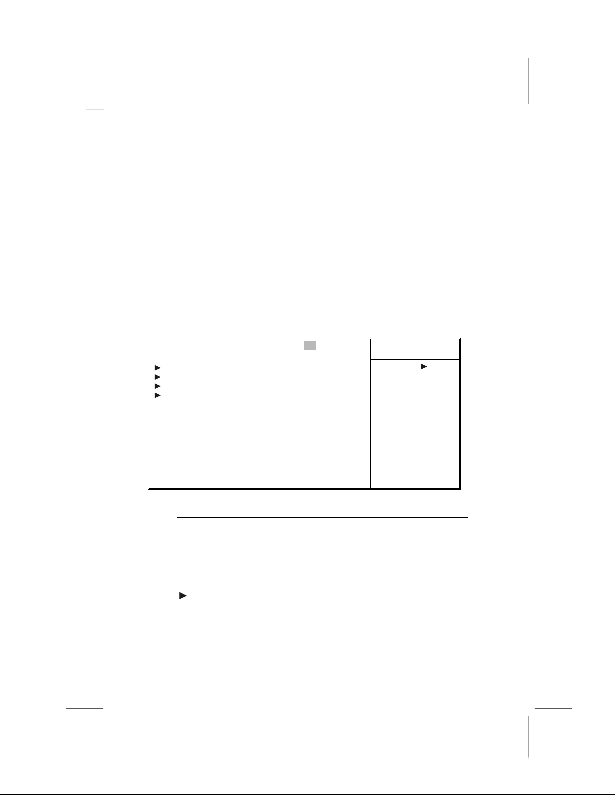
This chapter contains the following information:
!
!
!
Checklist
Compare the contents of yo ur mainboar d package wit h the stan dard checklist below . If any ite m is missing or appea rs damaged,
please contact the vendo r of your main board package.
Standard Items
! One mainboard
! One diskette drive ribbon cable and bracket
! One IDE drive ribbon cable and bracket
! This user’s manual
! Software support CD-ROM disc
Checklist
components that are shipped with this mainboard
Recommendations
manufacturer to help ensure reliability and performance
from this product
Features
make this one of the best value mainboards on the market
comprises a list of the standard and optional
lists some Do’s and Don’ts from the
highlights the functions and components that
2
Page 9

Recommendations
This mainboard automatically determines the CPU clock frequency and system bus frequency for the kind of processor that
you install. You may be able to change these automatic settings
by making changes to jumpers on the mainboard, or changing
the settings in the system Setup Utility. We strongly recommend
that you do not overclock the mainboard to run processors or
other components faster than their rated speed.
Warning: Overclocking components can adversely affect the reliability of the system and i nt roduce e rrors in to your system. Overclocking
can permanentl y dam age th e mainbo a rd by g ene rati ng e xce ss heat
in components that are run beyond the rate d limits .
Components on this mainboard can be damaged by discharges
of static electricity. Handle the board carefully holding it by the
edges. Do not flex or stress the circuit board. Keep the board in
its static-proof packing until you are ready to install it. Follow the
static guidelines given at the beginning of Chapter 2.
3
Page 10

Features
The key features of this mainboard are the wide range of processors that can be installed, and the high level of integration.
Value-class Processors
Functioning as a platform for a value PC, the MS7177C features
a Socket 370 that accommodates PPGA Celeron, Pentium III,
and Cyrix III processors. The MS7177C supports 66/100/133
MHz FSB speeds.
VIA North Bridge Chipset
This board features the VIA VT82C694X NB (North Bridge)
chipset, enabling synchronous and asynchronous frequency operation between the processor and the memory over a wide
frequency range. The NB chipset is optimized for Pentium III
processors at 66/100/133 MHz Front Side Bus (FSB) frequency
and supports 32-bit processor bus addressing.
The integrated DRAM controller supports up to four doublesided DIMMs consisting of EDO, SDRAM, or VCM SDRAM. The
NB chipset provides SDRAM with a 64-bit data interface.
The AGP interface is AGP specification Rev 2.0 compliant, and
supports 2x/4x/4x 3.3/1.5V devices. The PCI bus interface complies with PCI Rev. 2.2, and supports 3.3V and power supplies.
Five PCI bus masters are supported in addition to the host and
PCI-to-ISA I/O bridge.
VIA South Bridge Chipset
Note: The MS7177C supports two VIA South Bridge chipsets—
the VIA VT82C686A and the VIA VT82C686B. The VIA
VT82C686A is standard and supports UDMA33/66. The VIA
VT82C686B is optional and supports UDMA100.
The VIA VT82C686A SB (Sout h B ridge ) chip set comes in a 352- p in
BGA package. The P CI to I S A Bri dge ha s a n i nte g rated I SA bu s
controller with integrated DMA, timer, and interrupt controllers. The
VIA VT82C686A chip set sup ports UDMA 33/66 .
4
Page 11

As an option y ou can ge t the MS7177C with th e V IA V T8 2C6 86B
SB chipset, which support s UDMA100.
The Real Time Clock features extended 256 byte CMOS RAM
and a day and month alarm for the ACPI (Advanced Configuration and Power Interface).
There is an integrated USB controller with a built-in root hub and
four function ports. The integrated Ultra DMA33/66 master mode
EIDE controller with enhanced PCI bus commands.
The UltraDMA33/66 Master Mode PCI EIDE controller features
dual channel master mode PCI supporting Enhanced IDE (EIDE)
devices and employ transfer rates up to 33 MB/sec to cover PIO
mode 4, multi-word DMA mode 2 drives, and UltraDMA-33 interface. The SB chipset also supports ATAPI compliant devices
including DVD devices and four USB 1.1 ports for serial transfers at 12 or 1.5 Mbits/sec.
The integrated super IO controller supports two serial ports, an
IR port, parallel port, and floppy disk controller functions. There
is also system monitor support, providing system feedback of
voltage, temperature, and fan speed conditions.
Inexpensive Memory
The board has three DIMM sockets for the installation of 168-pin,
3.3V non-buffered DIMM memory modules. The DIMM memory
modules can be SDRAM or VCM memory chips.
4xAGP Graphics Adapter Slot
The MS7177C includes a 4xAGP slot that provides four times
the bandwidth of the original AGP specification. AGP technology
provides a direct connection between the graphics sub-system
and the processor so that the graphics do not have to compete
for processor time with other devices on the PCI bus.
The AGP design allows the graphics controller to use part of the
main memory when it needs it, for example, in handling the very
large texture maps required by virtual reality and 3D video
games and applications.
5
Page 12

AC 97 Audio Codec
The AC 97 Audio codec is compliant with the AC 97 2.1 specification, and supports 18-bit ADC (Analog Digital Converter) and
DAC (Digital Analog Converter) resolution as well as 18-bit
stereo full-duplex codec with independent and variable sampling
rates. Further features include support for four analog line-level
stereo inputs.
Expansion Options
Five 32-bit PCI slots, an AGP slot, and an AMR slot provide
plenty of expansion potential. The MS7177C PCI slots support
Ultra DMA33/66 bus mastering with transfer rates up to 33/66
MB/sec.
Integrated I/O
The mainboard has a full set of I/O ports and connectors. The
I/O template on the backplane includes two PS/2 ports for
mouse and keyboard, two serial port, one parallel port, one
MIDI/game port, two USB ports with an onboard header providing two extra USB ports, and audio jacks for microphone, line-in
and line-out. The board includes two PCI IDE channels and a
floppy disk drive interface.
Keyboard Power on Feature
Using the system BIOS setup program, you can configure the
system to turn on using a keyboard-typed password. A green
keyboard is not required.
Programmable Firmware
The mainboard includes Award BIOS that allows BIOS setting of
CPU parameters. This fully programmable firmware enhances
the system features and allows users to set such items as power
management, CPU and memory timing, and modem wake-up
alarms. The firmware can also be used to set parameters for
different processor clock speeds so that you don’t need to
change mainboard jumpers and switches.
This concludes Chapter 1. The next chapter will cover installing
and building a working system.
6
Page 13

CChhaapptteerr 22:: IInnssttaallllaattiioon
Quick Installation Table
This chapter explains how to successfully install the mainboard
into a computer case and build a working system. The installation procedure is as follows:
n
Quick Jumper
Setting
Reference
Before you
Begin
Preparing the
Mainboard
Installing Other
Hardware
Making
External
Connections
Provides a quick reference for the jumper
settings on this mainboard.
Provides advice on choosing a case,
avoiding static electricity damage, and setting jumpers.
Provides a guide to the mainboard and I/O
port locations, full details on the jumper
settings, and advice on installing the mainboard in the system case.
Provides guidance on installing essential
hardware: processor, memory, hard disk
drive, CD-ROM, floppy disk drive, and expansion cards.
Provides advice on using the external I/O
ports to install peripheral devices such as a
keyboard, a monitor, a mouse, a printer,
and loudspeakers.
7
Page 14
Quick Jumper Setting Reference
If you are familiar with most of the material in this chapter, you
can prepare the mainboard for installation by using this quick
reference to set the jumpers. A detailed description of the jumper setting appears later in this chapter.
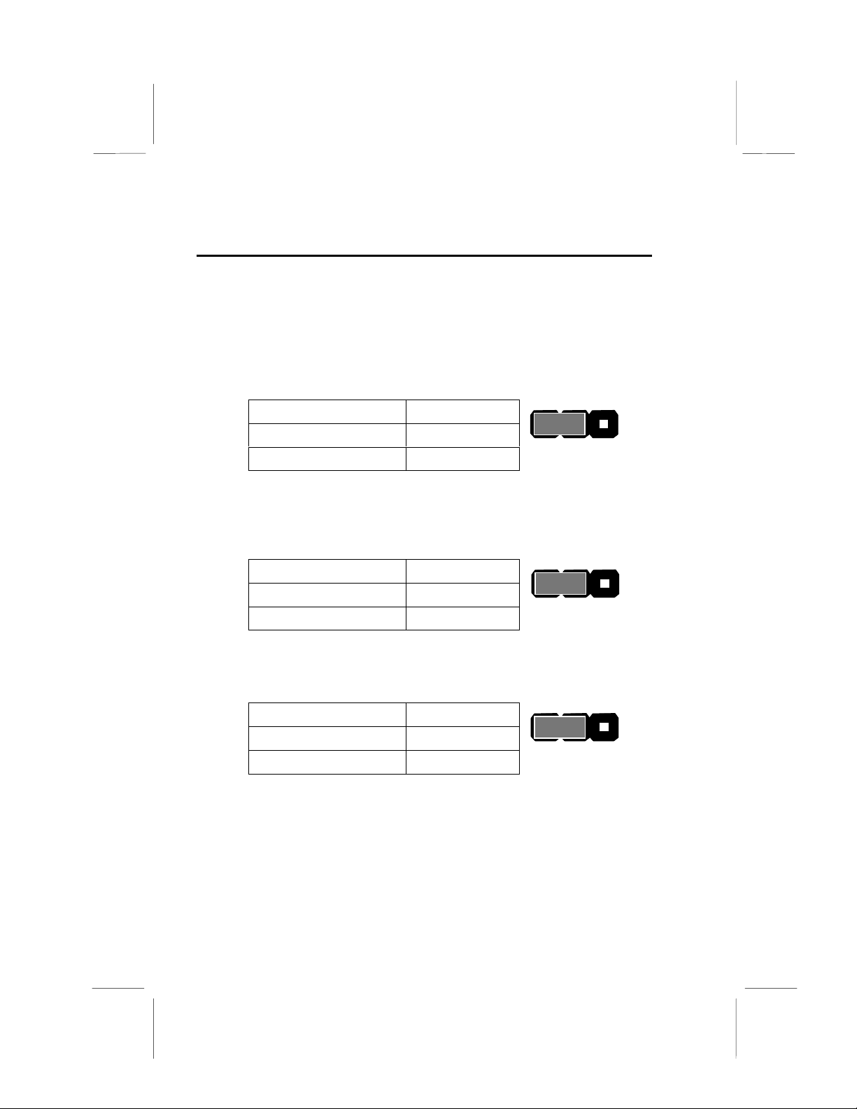
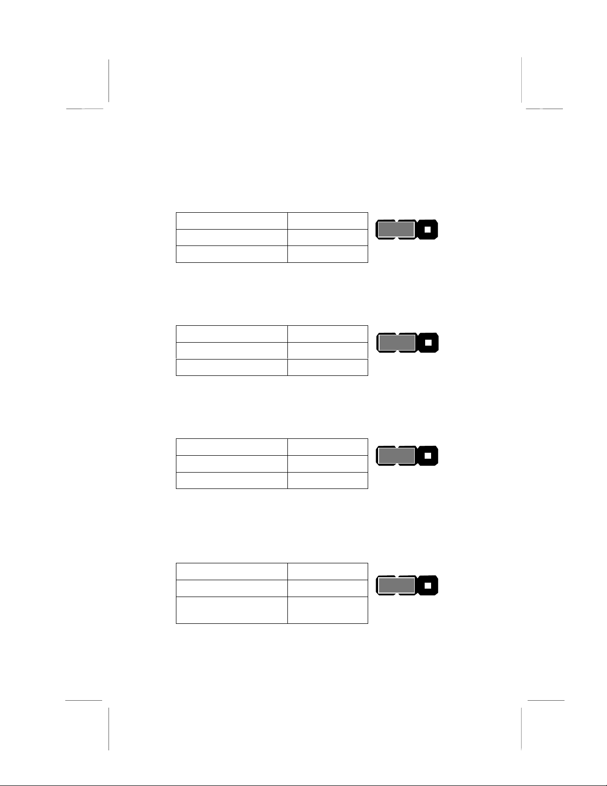
JP1: Clear CMOS jumper
Use this jumper to clear the contents of the CMOS memory.
Function Jumper Setting
Normal operation Short pins 1-2
Clear CMOS Short pins 2-3
1 2 3
JP1
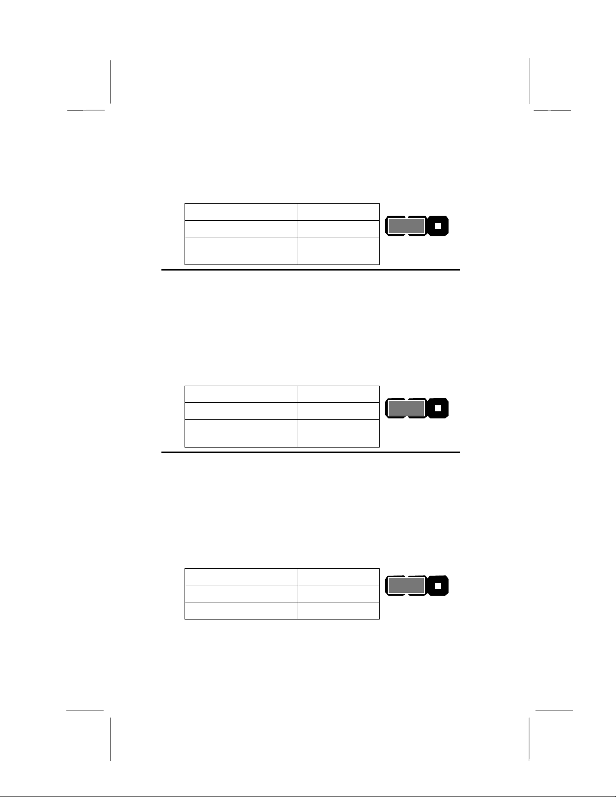
JP5: Suspend to RAM support enable/disable jumper
Use this jumper to enable or disable the Suspend to RAM (STR)
Function. You must also enable this function in the BIOS Setup
Utility. Refer to Chapter 3.
Function Jumper Setting
Enable Short pins 1-2
Disable Short pins 2-3
1 2 3
JP5
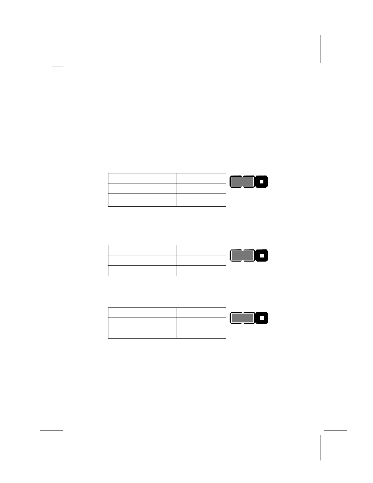
JP6: USB1 wake up jumper
Use this jumper to enabl e a signal to the USB port s (locat ed on the
I/O port panel) to wake up th e system fro m power saving mode.
Function Jumper Setting
Disable Short pins 1-2
Enable Short pins 2-3
1 2 3
JP6
8
Page 15
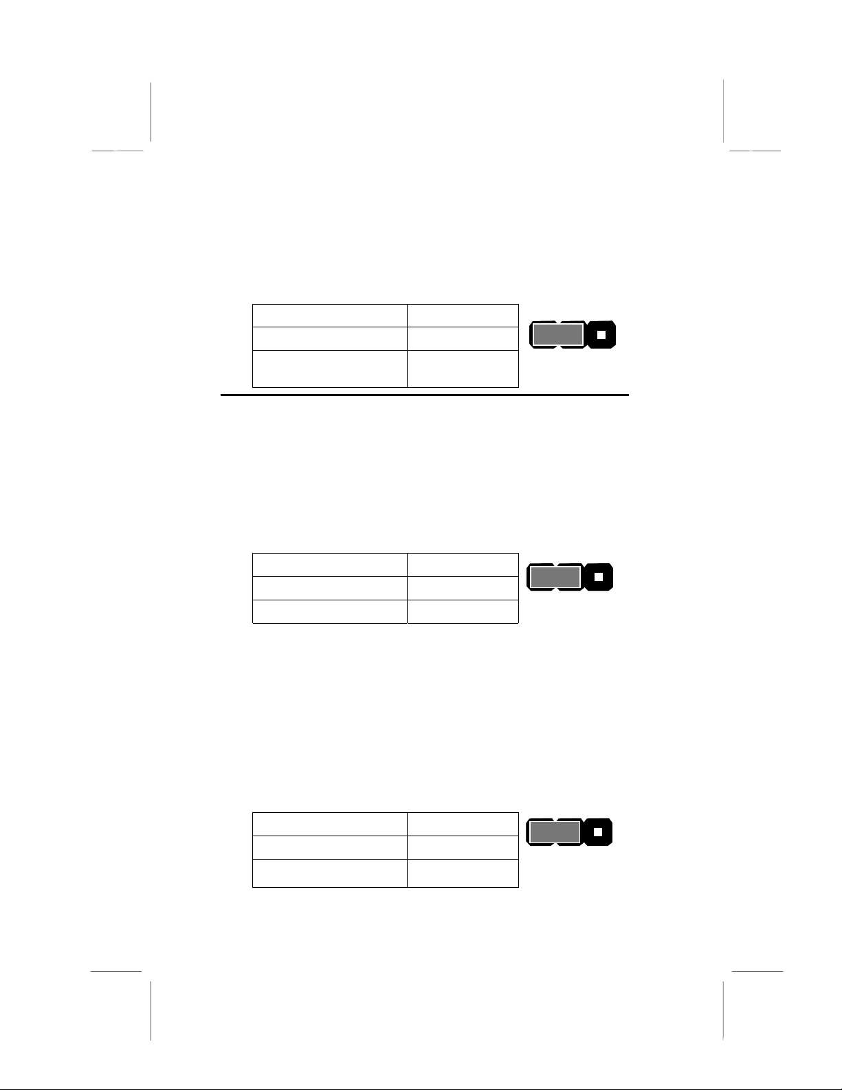
JP7: CPU frequency select jumper
Use this jumper to force a CPU that has a 66 MHz frontside bus
(FSB) to run at a 100 MHz FSB speed.
Function Jumper Setting
Normal operation Short pins 1-2
Force a 66 MHz FSB to
run at 100 MHz FSB
Short pins 2-3
1 2 3
Note: The CPU speed is determined by the CPU Host/PCI Clock
speed multiplied by the CPU Clock Ratio. Refer to the Frequency
Control Option in Chapter 3 for more information.
Forcing the CPU to run at a higher clock speed then it was rated
for is called overclocking and is not recommended.
JP8: CPU frequency select jumper
Use this jumper to force a CPU that has a 100 MHz frontside
bus (FSB) to run at a 133 MHz FSB speed.
Function Jumper Setting
Normal operation Short pins 1-2
Force a 100 MHz FSB to
run at 133 MHz FSB
Short pins 2-3
1 2 3
JP1
JP2
Note: The CPU speed is determined by the CPU Host/PCI Clock
speed multiplied by the CPU Clock Ratio. Refer to the Frequency
Control Option in Chapter 3 for more information.
Forcing the CPU to run at a higher clock speed then it was rated
for is called overclocking and is not recommended.
JP14: Onboard CODEC/AMR slot select jumper
Use this jumper to enable either the onboard codec or the AMR
slot (AMR1).
Function Jumper Setting
Onboard codec Short pins 1-2
AMR slot Short pins 2-3
1 2 3
9
JP14
Page 16
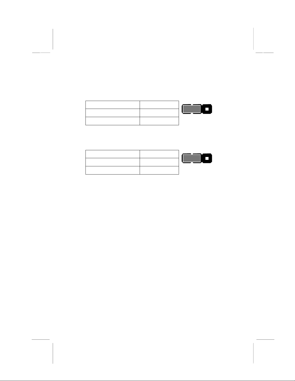
JP16: Dual color LED header
This header allows the user to install red and green LED indicators to indicate when the computer is in Suspend to RAM (STR)
or normal. Although the values are not predefined, red usually
indicates STR and green indicates nor mal.
JP17: USB2 wake up jumper
Use this jumper to enable a signal to the USB devices 3 and 4
(located on the front panel) to wake up the system from power
saving mode.
Function Jumper Setting
Disable Short pins 1-2
Enable Short pins 2-3
1 2 3
JP17
JP18: BIOS Flash protect jumper
Use this jumper to enable or disable the BIOS flash protection
on the mainboard. You should disable this jumper when you
want to flash the BIOS.
Function Jumper Setting
Disable Short pins 1-2
Enable Short pins 2-3
1 2 3
JP18
JP19: AMR codec mode
Use this jumper to define the AMR codec mode and avoid conflict with the onboard AC 97 codec.
Function Jumper Setting
Slave AMR card Short pins 1-2
Master AMR card Short pins 2-3
1 2 3
JP19
10
Page 17
PANEL1: Panel connectors for switches and indicators
Use the panel connector to implement the switches and indicators on your system case.
Panel connectors for switches and indicators
Function Pins
PANEL1
Power switch +22, 23
Hard disk LED Indicator +20, 21
Empty pin 19
23
Power Sw itch 22-23
HDD LED 20-21
Speaker +15, 16, 17, 18
Empty pin 14
Reset switch 12, 13
Speaker 15-16-17 -18
Empty pins 10, 11
Green LED indicator +7, +8, 9
Reset Switch 12-13
Empty pin 6
Sleep switch 4, 5
Power LED indicator +1, +2, 3
Green LED 7-8-9
PANEL1
Sleep Switch 4-5
Power LED 1-2-3
1
Note: The plus sign (+) indicates a pin which must be connected
to a positive voltage.
11
Page 18

Before You Begin
Before you begin to install your mainboard, take care not to
damage the product from static electricity. Ensure too that you
are installing the mainboard into a suitable case.
Static Electricity
In adverse conditions, static electricity can accumulate and discharge through the integrated circuits and silicon chips on this
product. These circuits and chips are sensitive and can be permanently damaged by static discharge.
• If possible, wear a grounding wrist strap clipped to a
safely grounded device during the installation.
• If you don’t have a wrist strap, discharge any static by
touching the metal case of a safely grounded device before beginning the installation.
• Leave all components inside their static-proof bags until
they are required for the installation procedure.
• Handle all circuit boards and electronic components
carefully. Hold boards by the edges only. Do not flex or
stress circuit boards.
Choosing a Case
The mainboard complies with the specifications for the Micro
ATX system case. Some features on the mainboard are implemented by cabling connectors on the mainboard to indicators
and switches on the system case. Ensure that your case supports all the features required. The mainboard can support one
or two floppy diskette drives and four enhanced IDE drives. Ensure that your case has sufficient power and space for all the
drives that you intend to install.
The mainboard has a set of I/O ports on the rear edge. Ensure
that your case has an I/O template that supports the I/O ports
and expansion slots.
12
Page 19
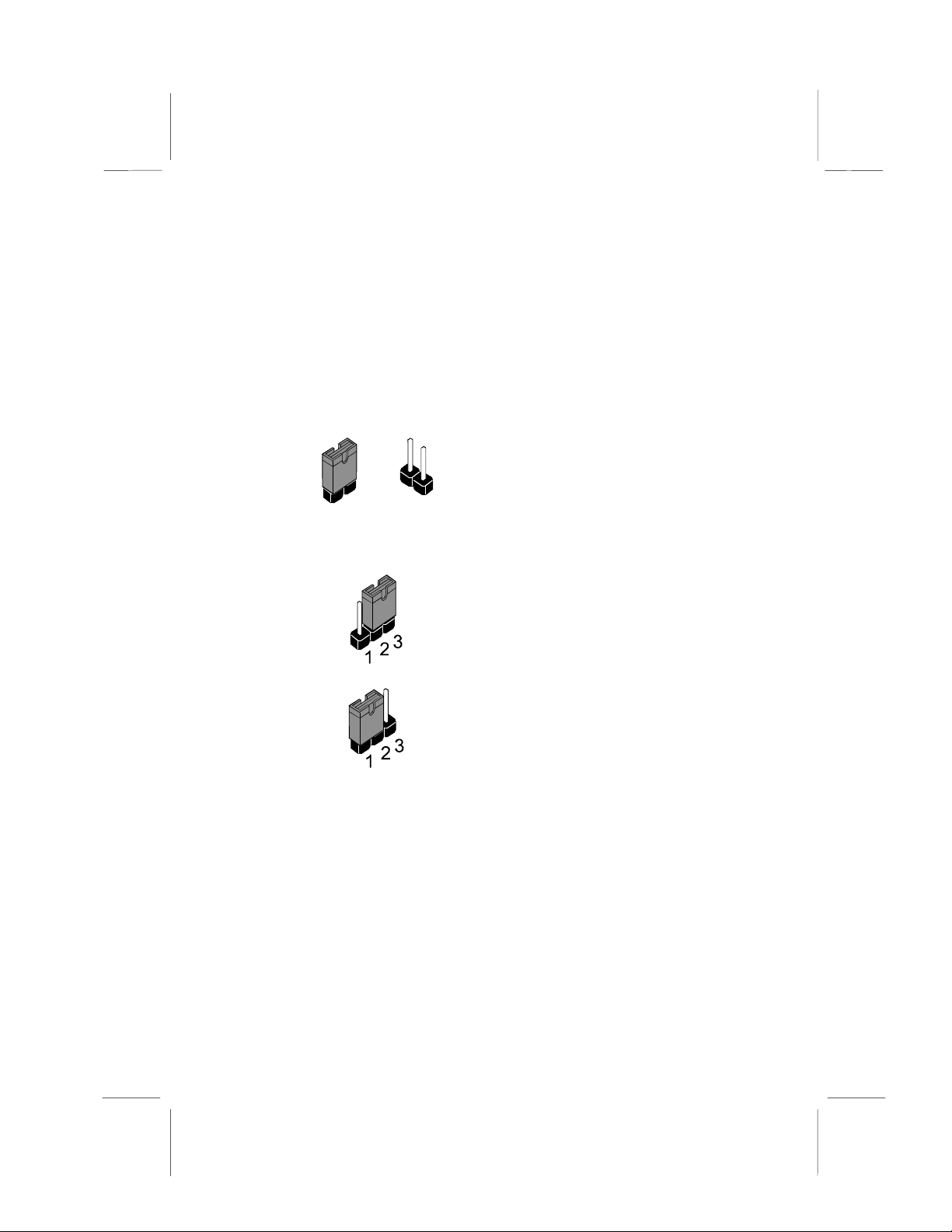
How to Set Jumpers
A jumper consists of two or more pins mounted on the mainboard. Some jumpers might be arranged in a series with each
pair of pins numbered differently. Jumpers are used to change
the electronic circuits on the mainboard. When a jumper cap (or
shunt) is placed on two jumper pins, the pins are SHORT. If the
jumper cap is removed (or placed on just a single pin), the pins
are OPEN.
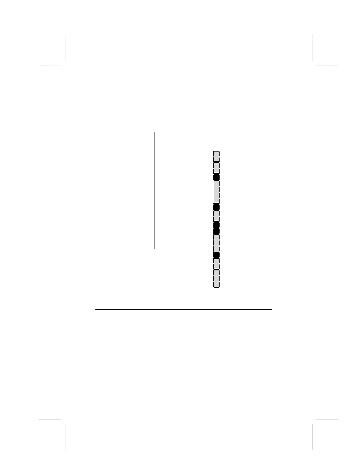
This illustration shows a 2-pin jumper.
When the jumper cap is placed on
both pins, the jumper is SHORT. If
you remove the jumper cap, or place
the jumper cap on just one pin, the
Short
Open
jumper is OPEN.
This illustration shows a 3-pin jumper.
The jumper cap is placed on pins 2
and 3, so this jumper setting is
SHORT PINS 2-3.
This illustration shows the same 3-pin
jumper. The jumper cap is placed on
pins 1 and 2, so this jumper setting is
SHORT PINS 1-2.
In this manual, all the jumper illustrations clearly show the pin
numbers. When you are setting the jumpers, make sure that the
jumper caps are placed on the correct pins to select the function
or feature that you want to enable or disable.
13
Page 20
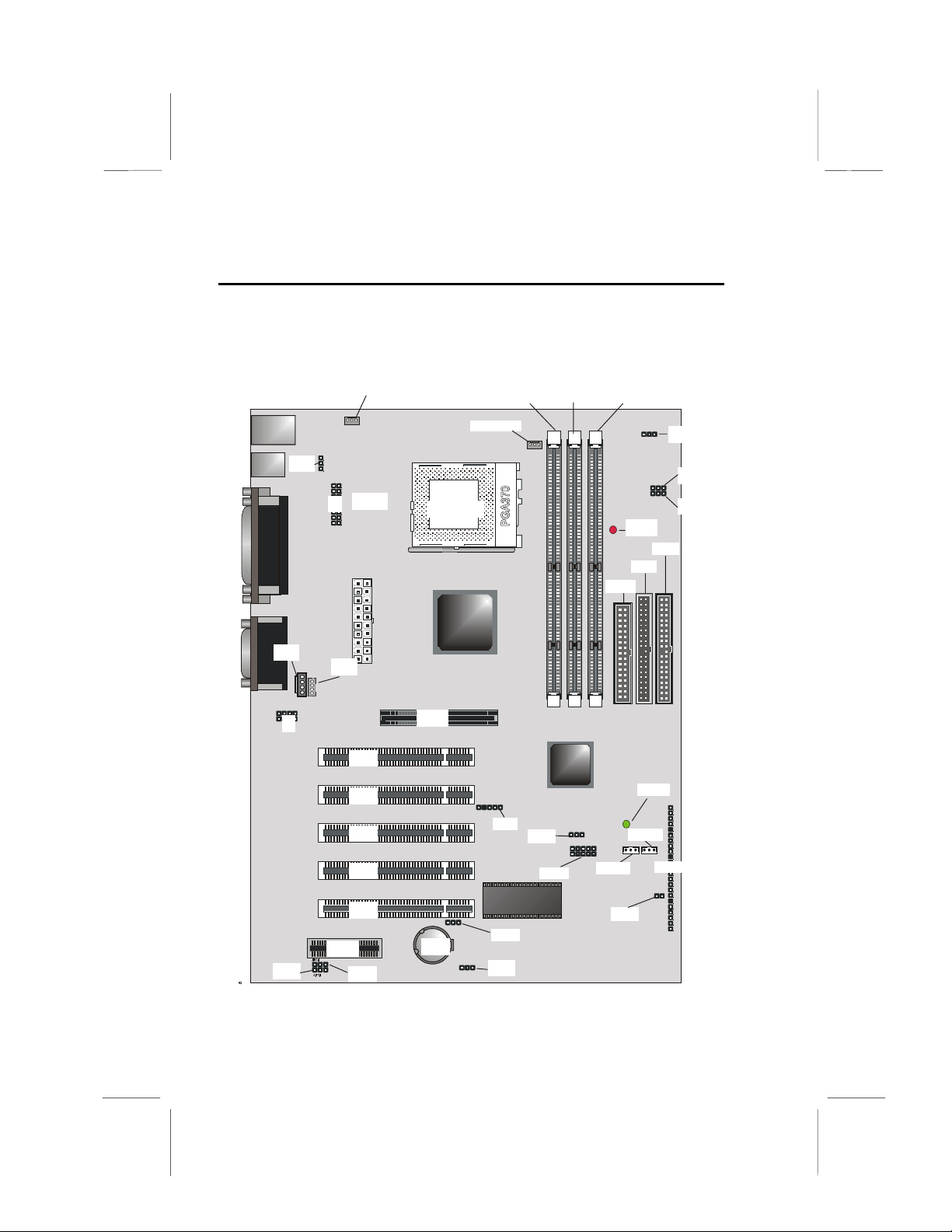
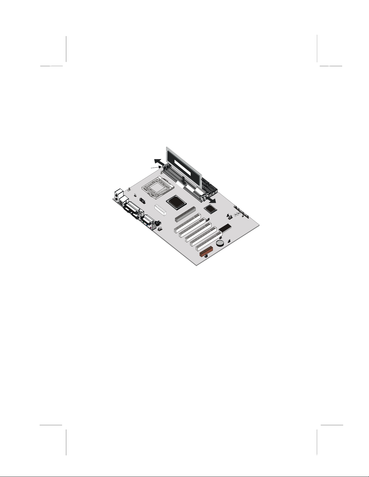
Preparing the Mainboard
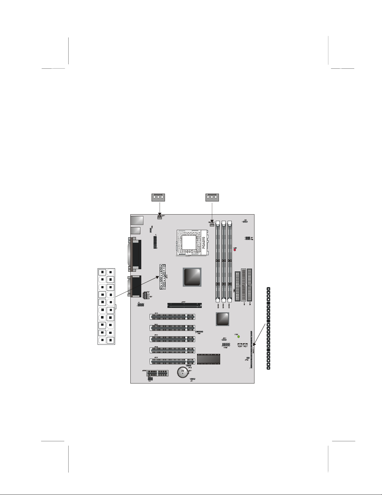
Mainboard Guide
Use the following illustration and key to identify the components
on your mainboard.
PWRFAN1
DIMM 1 DIMM 2 DIMM 3
PWRFAN1
LED1
1
LED1
JP5
JP5
JP7
1
JP7
1
JP8
JP8
JP6
CPUFAN1
JP6
1
CPUFAN1
J1
ATX1
J1
1
Socket 370
IDE2
IDE1
FDD1
ATX 1
CD1
CD2
CD1
FDD1
CD2
J2
1
J2
AGP1
AGP1
IDE2
DIMM1
DIMM2
DIMM3
IDE 1
PCI1
PCI1
PCI2
PCI2
1
PCI3
PCI3
PCI4
PCI4
PCI5
PCI5
AMR1
AMR1
1
1
JP19
DIMM1DIMM3DIMM2
PWRFAN1
PWRFAN1
JP2
PWRFAN1
JP15JP3
DIMM1DIMMDIMM2
JP6
VID1VID2
VID3VID4VID5
JP6
VID1VID2
VID3VID4VID5
PWRFAN1CPUFAN1
JP2
CPUFAN1
JP9JP7JP8
JP15JP3JP4JP5
CPUFAN1
ATX1
JP9JP7JP8JP10
JP4JP5
PPGA1
CPUFAN1
ATX1
ATX1
ATX1
LOCKFREE
VGA1PPGA1
FDD1
LOCKFREE
VGA1
FDD1
JP10
LTI1
J1
LTI1
FDD1IDE1IDE2
J1
CD1
LTI1
CD1CD2
CD1
LTI1
CD1CD2
CD2
JP1
JP1
FDD1IDE1IDE2
DIMM1
DIMM2DIMM3
DIMM1
DIMM2DIMM3
3V+
AGP1
PCI1
BT1J2
AGP1
IDE1
PCI1
BT1
3V+
AGP1
PCI1
CD2BT1J2
AGP1
IDE1
PCI1
BT1
AMR1
JP1
JP14
AMR1
SIR1
PANE
PCI2
AMR1
JP1
JP14
AMR1
SIR1
PANE
PCI2
PCI2
JP17JP16
SIR1
PCI2
JP17JP16
SIR1
JP14
3V
+
BT1
SIR1
SIR1
JP17
JP17
1
1
USB2
USB2
1
JP18
JP18
BT1
1
JP1
JP1
LED2
WOM1
JP16
LED2
WOL1
WOM1 WOL1
PANEL1
JP16
1
PANE L1
14
Page 21

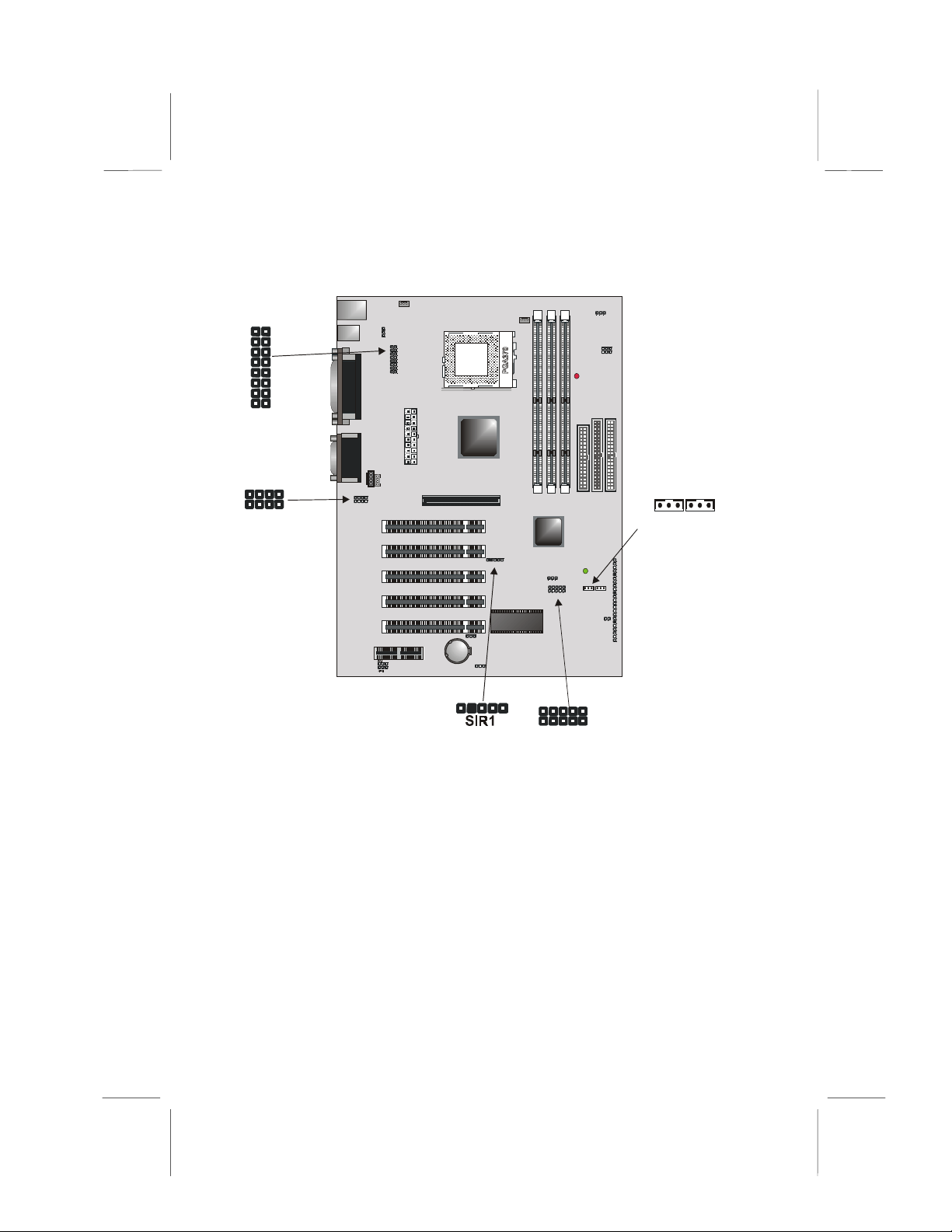
Key to Mainboard Components
Component Description
PWRFAN1 Power connector for case cooling fan
JP6 USB wake up select jumper
J1 Extra IR/KB/Mouse header
PGA370 CPU socket
CPUFAN1 Power connector for CPU cooling fan
DIMM 1, 2, 3 Three slots for 168-pin DRAM memory module
JP5 Suspend to RAM support jumper
JP7, 8, CPU frequency select jumper
LED1 3 VSB for SDRAM (red)
IDE1, IDE2 Primary and secondary IDE channels
FDD1 Connector for floppy disk drives
ATX1 Connector for ATX power supply
CD1 Audio connector for CD-ROM/DVD drive
CD2 Auxiliary connector for CD-ROM/DVD drive
J2 Extra MIC/Line-out header
BT1 3 volt battery for realtime clock
AGP1 Accelerated Graphics Port slot
PCI1 ~ PCI5 Five 32-bit PCI slots
JP14 On-board codec or AMR slot select jumper
AMR1 Audio modem riser (AMR) slot
JP19 AMR codec mode jumper
SIR1 SIR connector for infrared
JP1 Clear the system CMOS jumper
JP16 Dual color LED header
JP17 USB wake up jumper
JP18 BIOS flash protect jumper
PANEL1 Panel connector for switches and indicators
LED2 Power LED (green)
WOL1 Connector for LAN wake up
WOM1 Connector for modem wake up
USB2 Connector for USB port
Note: LED1 and LED 2
LED1: This red indicator warns you that the computer is still powered on and you should not install or uninstall memory modules.
LED2: This green indicator warns you that the computer is still active and you should not carry out any work on the mainboard.
15
Page 22
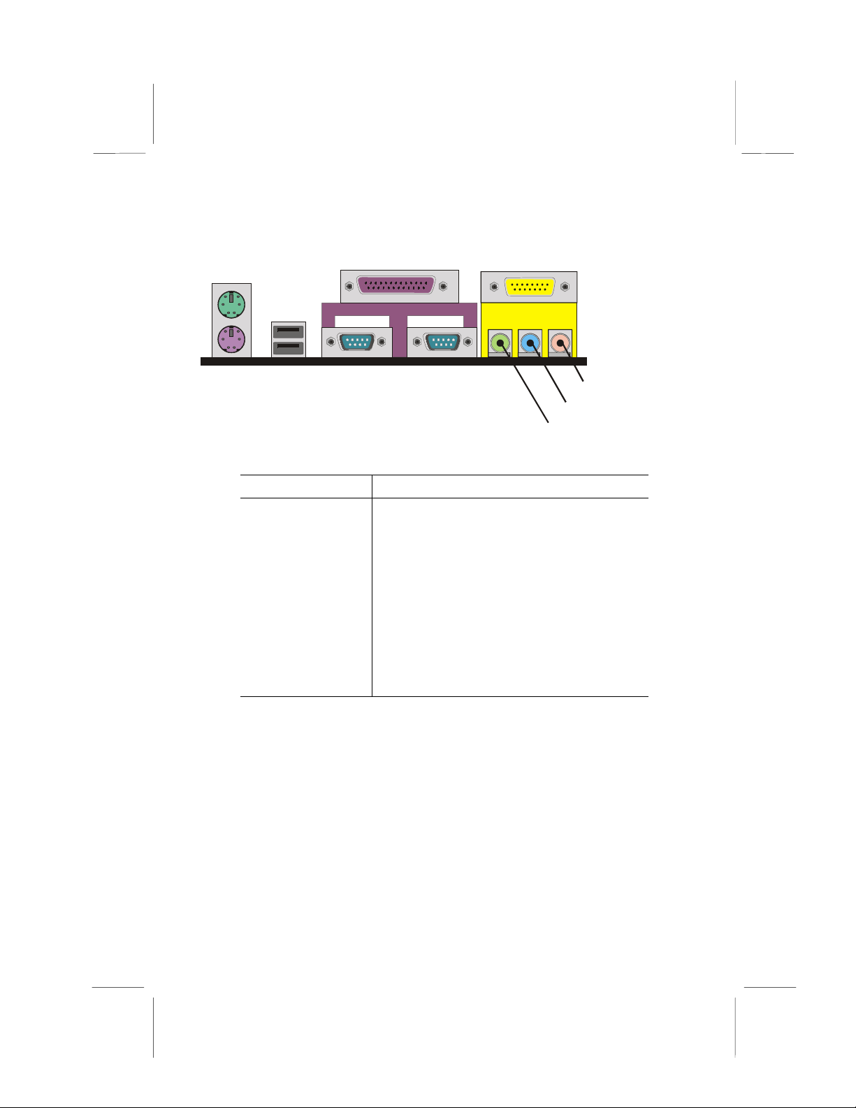
I/O Ports Side View
PS/2
mouse
PS/2
keyboard
Key to I/O Ports
Component Description
PS/2 mouse PS/2 port for pointing device (upper port)
PS/2 keyboard PS/2 port for keyboard (lower port)
USB ports Two stacked Universal Serial Bus ports
LPT1 External parallel port
COM1 External serial port COM 1
COM2 External serial port COM 2
Game port External MIDI/game port
Audio ports Audio jacks for (from left to right) line out, line
USB
ports
Pa r a lle l p o r t (L PT 1 )
Se rial p o rt
COM 1
Se rial p o rt
COM 2
in, microphone
Game port
Microphone
Line-in
Line-out
16
Page 23
Check the Jumper Settings
J
Check the mainboard jumpers to ensure that the board is configured correctly.
1
JP5
1
JP6
1
1
JP14
JP19
JP7
1
1
JP8
1
JP17
JP16
JP18
1
P1
1
JP1: Clear CMOS jumper
Use this jumper to clear the contents of the CMOS memory. You
may need to clear the CMOS memory if the settings in the BIOS
Setup Utility a re in co rre ct an d a re pr even tin g y ou r main bo ard from
operating. To clear the CM OS memory, di sconne ct all the power
cables from the mainboard and then move the jumper cap into the
Clear CMOS memory settin g for a few second s. CMOS i s clea red.
17
Page 24
Return the jumper cap to the Normal operation setting. Reconnect the power cables and start the system. When the POST
starts, press the delete key to start the BIOS Setup Utility and
reload BIOS optimal settings. Refer to Chapter 3 for information
on BIOS.
Function Jumper Setting
Normal operation Short pins 1-2
Clear CMOS Short pins 2-3
1 2 3
JP1
JP5: Suspend to RAM support enable/disable jumper
Use this jumper to enable or disable the Suspend to RAM (STR)
Function. You must also enable this function in the BIOS Setup
Utility. Refer to Chapter 3.
Function Jumper Setting
Enable Short pins 1-2
Disable Short pins 2-3
1 2 3
JP5
JP6: USB1 wake up jumper
Use this jumper to enable a signal to the USB ports (located on
the I/O port panel) to wake up the system from power saving
mode.
Function Jumper Setting
Disable Short pins 1-2
Enable Short pins 2-3
1 2 3
JP6
JP7: CPU frequency select jumper
This jumper enables you to force the CPU to clock at a higher
frequency than it is rated. Short pins 2 and 3 to force the CPU to
run at a 100 MHz FSB instead of a 66 MHz FSB. We recommend that you leave the jumper on the normal operation setting.
Function Jumper Setting
Normal Short pins 1-2
Force 66 MHz FSB to
run at 100 MHz FSB.
Short pins 2-3
1 2 3
JP7
18
Page 25
JP8: CPU frequency select jumper
This jumper enables you to force the CPU to clock at a higher
frequency than it is rated. Short pins 2 and 3 to force the CPU to
run at a 133 MHz FSB instead of a 100 MHz FSB. We recommend that you leave the jumper on the normal operation setting.
Function Jumper Setting
Normal Short pins 1-2
Force 100 MHz FSB to
run at 133 MHz FSB
Short pins 2-3
1 2 3
Note: The CPU speed is determined by the CPU Host/PCI Clock
speed multiplied by the CPU Clock Ratio. Refer to the Frequency
Control Option in Chapter 3 for more information.
Forcing the CPU to run at a higher clock speed then it was rated
for is called overclocking and is not recommended.
JP14: Onboard CODEC/AMR slot select jumper
Use this jumper to enable either the onboard codec or the AMR
slot (AMR1).
JP8
Function Jumper Setting
Onboard codec Short pins 1-2
AMR slot Short pins 2-3
1 2 3
JP14
JP16: Dual color LED header
This header allows the user to install red and green LED indicators to indicate when the computer is in Suspend to RAM (STR)
or normal. Although the values are not predefined, red usually
indicates STR and green indicates nor mal.
JP17: USB2 wake up jumper
Use this jumper to enable a signal to the USB devices 3 and 4
(located on the front panel) to wake up the system from power
saving mode.
Function Jumper Setting
Disable Short pins 1-2
Enable Short pins 2-3
1 2 3
JP17
19
Page 26
JP18: BIOS Flash protect jumper
Use this jumper to enable or disable the BIOS flash protection
on the mainboard. You should disable this jumper when you
want to flash the BIOS.
Function Jumper Setting
Disable Short pins 1-2
Enable Short pins 2-3
1 2 3
JP18
JP19: AMR codec mode
Use this jumper to define the AMR codec mode and avoid conflict with the onboard AC 97 codec.
Function Jumper Setting
Slave AMR card Short pins 1-2
Master AMR card Short pins 2-3
1 2 3
JP19
20
Page 27

Installing the Mainboard in a Case
p
Most system cases have mounting brackets installed in the case,
which correspond to the holes in the mainboard. Place the
mainboard over the mounting brackets and secure the mainboard into the mounting brackets with screws.
Most cases have a choice of I/O templates in the rear panel.
Make sure that the I/O template in the case matches the I/O
ports installed on the rear edge of the mainboard.
This illustration
shows a mainboard
installed in a standard desktop case.
Note: Do not overtighten the screws
as this can stress
the mainboard.
This illustration
shows a mainboard
installed in a towertype case.
Power
Supply Unit
I/O
late
Tem
Power Supply Unit
I/O
Template
Expansion
Slots
Drive
Cage
Drive
Cage
Expansion
Slots
21
Page 28
Connecting Internal Components
C
After you have installed the mainboard into the system case,
connect the power cable from the case power supply unit to the
mainboard power connector ATX1.
Your case and CPU might have cooling fans attached to provide
adequate ventilation to the system. Connect the CPU fan to the
12-volt connector CPUFAN1. Connect the case fan to the 12volt power supply connector PWRFAN1. After you have connected the power supply and the cooling fans, connect the case
switches and indicators to the PANEL1 connectors.
AT X1
PWRFAN1
PUFAN1
PANEL1
1
22
Page 29

Panel Connector
The mainboard PANEL connector has a standard set of switch
and indicator connectors that are commonly found on ATX system cases. Use the illustration below to make the correct
connections to the case switches and indicators.
Panel connectors for switches and indicators
Function Pins
PANEL1
Power switch +22, 23
Hard disk LED Indicator +20, 21
Empty pin 19
Speaker +15, 16, 17, 18
Empty pin 14
Reset switch 12, 13
Empty pins 10, 11
Green LED indicator +7, +8, 9
Empty pin 6
Sleep switch 4, 5
Power LED indicator +1, +2, 3
23
Power Sw itch 22-23
HDD LED 20-21
Speaker 15-16-17 -18
Reset Switch 12-13
Green LED 7-8-9
PANEL1
Sleep Switch 4-5
Power LED 1-2-3
1
Note: The plus sign (+) indicates a pin which must be connected
to a positive voltage.
23
Page 30

Installing Other Hard wa re
C
Install the essential hardw are requi red to get you r system sta rted.
Installing the Processor
This mainboard has a Socket 370 processor socket. To choose
a processor, you need to consider the performance requirements of the system and the price of the processor.
Performance is based on the processor design, the clock speed
and system bus frequency of the processor, and the quantity of
internal cache memory and external cache memory. Higher
clock speeds and larger amounts of cache memory deliver
greater performance.
Installation Procedure
Follow the steps below to install a processor on your mainboard:
PUFAN1
(CPU fan)
CPU socket
Pin-1 corner
Locking lever
1. On the mainboard, locate the Socket 370 and CPU cooling
fan CPUFAN1.
24
Page 31

2. On the Socket 370, pull the locking lever away from the
socket to unhook it and then raise the locking lever to the
upright position.
3. Identify the pin-1 corner on the Socket 370 and the pin-1
corner on the processor. The socket pin-1 corner is adjacent
to the handle of the locking lever. The processor pin-1 corner is beveled.
4. Matching the pin-1 corners, drop the processor into the
socket. No force is required and the processor should seat
into the socket easily.
5. Swing the locking lever down and hook it under the latch on
the edge of the socket. This locks the processor in place.
6. Locate the power cable on the heatsink/cooling fan assembly that is attached to the top of the processor.
7. Plug the power cable into the CPU cooling CPUFAN1 12Vpower supply on the mainboard.
CPU fan
connector
CPUFAN1
Socket 370 with
locking lever in
upright position
Socket 370
processor with
heatsink/cooling
fan attached
The mainboard must be configured to deliver the correct clock
speed and the correct system bus for the kind of processor that you
have installed. You can do this by using the syste m Setup Utility .
The first time you start the system, immediately enter the setup
system and make the appropriate settings. Usually, you can automatically configure the CPU by using the CPU & BIOS Features
page of the Se tup Utili ty. See Chapter 3 for more i n for mation.
25
Page 32

Install the Memory Modules
For this mainboard, you must use 168-pin 3.3V non-buffered
Dual In-line Memory Modules (DIMMs). The memory chips must
be standard or registered SDRAM and VC M SDRAM m em ory
chips. The memory bus can run at 66 MHz, 100 MHz, or 133
MHz. If your processor operates over a 133 MHz system bus,
you can install PC133 or PC100 memory that operates over a
133 or 100 MHz bus. If your processor operates over a 100 MHz
system bus, you can install memory that operates over a
133MHz, 100 MHz or 66MHz bus. If your processor operates
over a 66MHz, you can only install memory chips that operate at
66MHz or 100MHz.
Supported Memory Configurations
The following table shows the memory configurations supported:
Technology Configuration # of Row
Addrs
Bits
64 Mbit 8M x 8 12 8 2 4 KB
64 Mbit 4M x 16 12 9 2 2 KB
128 Mbit 32M x 4 12 11 2 16 KB
128 Mbit 16M x 8 12 10 2 8 KB
Note:
32M x 4 128 Mbit is for registered DIMMs only, 4M x 16 64 Mbit sup-
port is for unbuffered DIMMs only.
# of Col
Addrs
Bits
# of Bank
Addrs
Bits
Page
Size
The following table shows the maximum memory for DIMM
based platforms:
1 DIMM 2 DIMMs 3 DIMMs
DRAM Configuration
64 Mbit 8M x 8 64 MB 128 MB 128 MB 256 MB 192 MB 384 MB
64 Mbit 4M x 16 32 MB 64 MB 64 MB 128 MB 96 MB 192 MB
128 Mbit 16M x 8 128 MB 256 MB 256 MB 512 MB 384 MB 768 MB
128 Mbit 32M x 4 256 MB 512 MB 512 MB 1024 MB 768 MB 1536 MB
•
Notes:
Single-sided DIMMs use one SDRAM row. (SS = Single-side)
•
Double-sided DIMMs use two SDRAM rows. (DS = Double-side)
•
This board supports a max imum of 512 M B
SS DS SS DS SS DS
26
Page 33
Installation Procedure
There are three slots for memory modules. You must install at
least one module, and it makes no difference which slot you use
to install the module. Each module can be populated with from
32 MB to 512 MB of memory; total memory capacity is 1.5 GB.
1. Locate the DIM M slots on the m ainbo ard.
Memory module
Locking latches
D
I
M
M
D
1
I
M
M
D
I
2
M
M
3
2. The DIMM slots are keyed with notches and the DIMMs are
keyed with cutouts so that they can only be installed correctly. Check that the cutouts on the DIMM module edge
connector match the notches in the DIMM slot.
3. Push the latches on each side of the DIMM slot down.
4. Install the DIMM module into the slot and press it firmly
down so that it seats correctly. The latches at either side of
the slot will be levered upwards and latch on to the edges of
the DIMM when it is installed correctly.
27
Page 34

Installing a Hard Disk Drive and CD-ROM
This section describes how to install IDE devices such as a hard
disk drive and a CD-ROM drive.
Note: Ribbon cable connectors are usually keyed so that they can
only be installed correctly on the device connector. If the connector is not keyed, make sure that you match the pin-1 side of the
cable connector with the pin-1 side of the device connector. Each
connector has the pin-1 side clearly marked. The pin-1 side of
each ribbon cable is always marked with a colored stripe on the
cable.
About IDE Devices
Your mainboard has a primary IDE channel interface (IDE1) and
a secondary IDE interface (IDE2). The mainboard ships with one
IDE ribbon cable that supports one or two IDE devices. All IDE
devices have jumpers or switches that can be used to set the
IDE device as MASTER or SLAVE.
If you install two IDE devices on one cable, you must make sure
that one device is set to MASTER and the other device is set to
SLAVE. The documentation of your IDE device explains how to
do this.
If you want to install more than two IDE devices, obtain a second
IDE cable and you can add two more devices to the secondary
IDE channel. If there are two devices on the cable, make one
MASTER and one SLAVE.
About UDMA
This board supports UltraDMA 33/66 (or UDMA 100 with the optional VIA VT82C686B chipset). UDMA is a technology that
speeds the performance of devices in the IDE channel. We recommend that you install IDE devices that support UDMA, and
use IDE cables that support UDMA.
Note: The MS7177C supports two VIA South Bridge chipsets—
the VIA VT82C686A and the VIA VT82C686B. The VIA
VT82C686A is standard and supports UDMA33/66. The VIA
VT82C686B is optional and supports UDMA100.
28
Page 35
Installing a Hard Disk Drive
1. Install the hard disk drive into the drive cage in your system
case.
2. Plug the IDE cable into the primary IDE channel on the
mainboard IDE1.
3. Plug one of the connectors on the IDE cable into the IDE
connector on the back edge of the hard disk drive. It doesn’t
matter which connector on the cable that you use. Make
sure that you have the pin-1 side of the cable matched with
the pin-1 side of the connector.
4. Plug a power cable from the case power supply unit into the
power connector on the back edge of the hard disk drive.
5. When you first start up your system, go immediately to the
Setup Utility and use the IDE Hard Disk Auto Detect feature
to configure the IDE devices that you have installed. See
Chapter 3 for more information.
IDE connector
IDE ribbon
cable
ID E 2
29
Hard disk
drive
Power
connector
ID E 1
Page 36

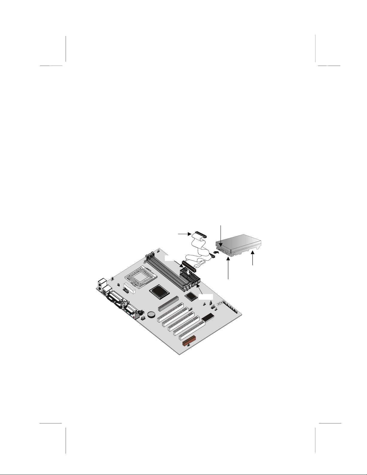
Installing a CD-ROM/DVD Drive
1. Install the CD-ROM/DVD drive into the drive cage in your
system case. Plug the IDE cable into the primary IDE channel on the mainboard IDE1.
2. Plug one of the connectors on the IDE cable into the IDE
connector on the back edge of the CD-ROM/DVD drive. It
doesn’t matter which connector on the cable that you use.
Make sure that you have the pin-1 side of the cable matched
with the pin-1 side of the connector.
3. Plug a power cable from the case power supply unit into the
power connector on the back edge of the CD-ROM/DVD
drive.
4. Use the audio cable provided with the CD-ROM/DVD drive
to connect the audio connector on the rear edge of the CDROM/DVD drive to the one of the two audio-in connectors
CDIN1 and CDIN2 on the mainboard.
5. When you first start up your system, go immediately to the
Setup Utility and use the IDE Hard Disk Auto Detect feature
to configure the IDE devices that you have installed. See
Chapter 3 for more information.
IDE
connector
Audio
connector
IDE ribbon
cable
Hard disk
drive
CD2
CD1
IDE 2
30
Power
connector
IDE 1
CD-ROM/DVD
drive
Page 37

Installing a Floppy Diskette Drive
The mainboard has a floppy diskette drive interface and it ships
with a diskette drive ribbon cable that supports one or two floppy
diskette drives. You can install a 5.25-inch drive and a 3.5-inch
drive with various capacities. The floppy diskette drive cable has
one type of connector for a 5.25-inch drive and another type of
connector for a 5.25-inch drive
1. Install the floppy diskette drive into the drive cage in your
system case. Plug the diskette drive cable into the diskette
drive interface on the mainboard FDD1.
2. Plug one of the connectors on the diskette drive cable into
the data connector on the back edge of the floppy diskette
drive. Make sure that you have the pin-1 side of the cable
matched with the pin-1 side of the connector.
3. Plug a power cable from the case power supply unit into the
power connector on the back edge of the diskette drive.
4. When you first start up your system, go immediately to the
Setup Utility and use the Standard page to configure the
floppy diskette drives that you have installed. See Chapter 3
for more information.
Data
connector
Floppy diskette
ribbon cable
Power
connector
Floppy diskette
drive
31
FDD1
Page 38

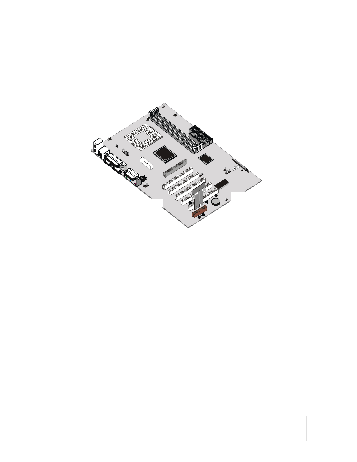
Using the Expansion Slots
This mainboard has five 32-bit PCI expansion slots, one 4xAGP
slot, and an AMR slot.
PCI Slots:
have the 32-bit PCI (Peripheral Components Interconnect) interface.
AGP Slot:
that supports the 4xAGP specification and has the 4xAGP edge
connector.
AMR S lot :
insert an AMR card.
AGP slot
The PCI slots can be used to install add-in cards that
The 4xAGP can be used to install a graphics adapter
The Audio Modem Riser (AMR) slot can be used to
PCI slots
AMR slot
32
Page 39

1. Before installing an expansion card, check the documenta-
C
tion for the card carefully. If the card is not Plug and Play,
you may have to manually configure the card before installation.
PCI
add-in card
Metal
bracket
Edge
onnector
2. Remove the blanking plate from the slot in the system case
that corresponds to the expansion slot that you are going to
use.
3. Install the edge connector of the add-in card into the expansion slot. Press down quite firmly to ensure that the edge
connector is correctly seated in the slot.
4. Secure the metal bracket of the card in the empty slot in the
system case wit h a screw.
5. For some add-in cards, for example graphics adapters and
network adapters, you have to install drivers and software
before you can begin using the add-in card.
PCI slot
33
Page 40
The following illustration shows how to insert an AMR card:
Edge
AMR card
Connector
AMR slot
34
Page 41
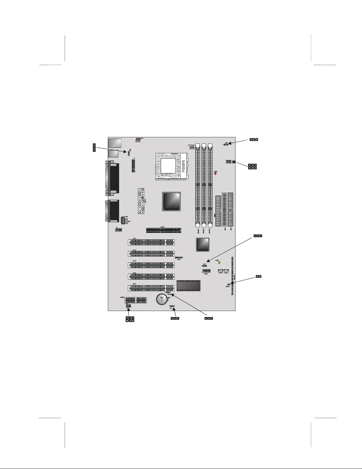
Add-in Card Options
US
J1
PWRFAN1
JP6
1
J1
1
CPUFAN1
JP5
1
1
JP7
1
JP8
LED1
1
ATX1
CD1
CD2
J2
1
J2
1
PCI1
PCI2
PCI3
PCI4
PCI5
AMR1
1
1
AGP1
1
SIR1
1
JP18
BT1
3V
+
1
JP1
FDD1
IDE1
DIMM1
DIMM2
DIMM3
IDE2
WOM1 WOL1
LED2
JP17
1
1
WOM1 WOL1
USB2
PANEL1
JP16
1
1
1
B2
J1: Extra IR/keyboard/mouse header
This mainboard provides a second infrared, keyboard, and
mouse header, giving the option of installing second infrared,
keyboard, and mouse ports on the front panel. Depending on
your case and system configuration this connector may be more
suitable as the sole IR port connector.
J2: Extra MIC/Line-out header
This header allows the user to install auxiliary front-oriented microphone and line-out ports for easier access.
35
Page 42

SIR1: Infrared Port
This mainboard can support a Serial Infrared (SIR) data port. Infrared ports allow the wireless exchange of information between
your computer and similarly equipped devices such as printers,
laptops, Personal Digital Assistants (PDA), and other desktop
computers.
USB2: USB ports 3/4 connector
Some cases come with USB ports on the front panel. If your
case has these ports, you can connect them to the USB2 connector.
WOM1: Wake On Modem
If you have installed a fax/modem card, you can use the cable
provided with the card to plug into the WOM1 connector on the
mainboard. This is the Wake On Modem feature. When your
system is in a power–saving mode, any incoming calls to the
modem automatically resume the system. You must enable this
item using the Power Management page of the setup utility. See
Chapter 3 for more information.
WOL1: Wake On LAN
If you have installed a network adapter (LAN adapter), you can
use the cable provided with the card to plug into the WOL connector on the mainboard. This is the Wake On LAN feature.
When your system is in a power–saving mode, any traffic
through the network automatically resumes the system. You
must enable this item using the Power Management page of the
Setup Utility. See Chapter 3 for more information.
36
Page 43

Making External Connections
After you have installed the mainboard, make the connections to
the external ports.
PS/2
mouse
PS/2
keyboard
1. The mainboard has a stack of two PS/2 mini-DIN ports. The
2. Use the USB ports to connect to USB devices.
3. LPT1 is a parallel port that can be used by printers or other
4. COM1 and COM2 are serial ports that can be used by serial
5. You can use the game port to connect a joystick or a MIDI
6. Three audio ports are provided. The left side jack is for a
USB
ports
Pa r alle l po rt ( L P T 1 )
Se ria l p o rt
COM 1
Se ria l p o rt
COM 2
Game port
Microphone
Line-in
Line-out
upper port can be used by a PS/2 mouse or pointing device.
The lower port can be used by a PS/2 keyboard.
parallel communications devices. The system identifies the
parallel port as LPT1.
devices such as mice or fax/modems. COM1 is identified by
the system as COM1/3. COM2 is identified by the system as
COM2/4.
device to your system.
stereo line-out signal. The middle jack is for a stereo line-in
signal. The right side jack is for a microphone.
37
Page 44

External Connector Color Coding
To help identify the external connectors, many connectors now
use standard colors as shown in the table below.
Connector Color
Analog VGA Blue
Audio line in Light blue
Audio line out Lime
Digital monitor / flat panel White
IEEE 1394 Grey
Microphone Pink
MIDI/Game Gold
Parallel Burgundy
PS/2 compatible keyboard Purple
PS/2 compatible mouse Green
Serial Teal or Turquoise
Speaker out/subwoofer Orange
Right-to-left speaker Brown
USB Black
Video out Yellow
SCSI, network, telephone, modem None
38
Page 45

CChhaapptteerr 33:: SSeettuup
p
About the Setup Utility
The computer employs the latest Award BIOS CMOS chip with
support for Windows Plug and Play. This CMOS chip contains
the ROM setup instructions for configuring the mainboard’s
BIOS. The BIOS (Basic Input and Output System) Setup Utility
is a ROM-based configuration utility that displays the system’s
configuration status and provides you with a tool to set system
parameters. These parameters are stored in non-volatile batterybacked-up CMOS RAM that saves this information even when
the power is turned off. When the system is turned back on, the
system is configured with the values found in CMOS.
Using easy-to-use pull down menus, you can configure such
items as:
• Hard drives, diskette drives, and peripherals
• Video display type and display options
• Password protection from unauthorized use
• Power management features
The settings made in the Setup Utility intimately affect how the
computer performs. It is important, therefore, first to try to understand all the Setup Utility’s options, and second, to make
settings appropriate for the way you use the computer. This
chapter guides you through the Setup Utility by providing clear
explanations for all Setup Utility options.
39
Page 46

A standard configuration has already been set in the Setup Utility, so you will very likely have little to worry about for now.
However, we recommend that you read this chapter just in case
you need to make any changes in the future.
This program should be executed under the following conditions:
• When changing the system configuration
• When a configuration error is detected by the system and
you are prompted to make changes to the Setup Utility
• When resetting the system clock
• When redefining the communication ports to prevent any
conflicts
• When making changes to the Power Management con-
figuration
• When changing the password or making other changes
to the security setup
Normally, running the Setup Utility is needed when the system
hardware is not consistent with the information contained in the
CMOS RAM, whenever the CMOS RAM has lost power, or the
system features need to be changed.
Entering the Setup Utility
When the system is powered on, the BIOS will enter the PowerOn Self Test (POST) routines. These routines perform various
diagnostic checks; if an error is encountered, the error will be
reported in one of two different ways:
1.
If the error occurs before the display device is initialized,
a series of beeps will be transmitted.
2.
If the error occurs after the display device is initialized,
the screen will display an error mess age.
40
Page 47

After the POST routines are completed, the following message
appears:
Press DEL to enter SETUP
To access the Award BIOS Setup Utility, press the delete key to
display the “CMOS Setup Utility” screen:
CMOS Setup Utility – Copyright (C) 1984 – 2000 Award Software
Standard CMOS Features
Advanced BIO S Features
Advanced Chi pset Features
Integrated Peripheral s
Power Management Setup
PnP/PCI Configurations
PC Health Stat us
Esc : Quit F9 : Menu in BIOS
F10 : Save & Exit Setup
Time, Date, Hard Disk Type . . .
Frequency/Voltage Control
Load Fail-Safe Def aul ts
Load Optimized Defa ul ts
Set Supervisor Password
Set User Password
Save & Exit Setup
Exit Without Saving
↑↑↑↑ ↓↓↓↓ →→→→
←←←←
: Select Item
This screen provides access to the utility’s various functions.
BIOS Navigation Keys
Listed below are explanations of the keys displayed at the bottom
of the screens:
Key Function
Esc
←←←← ↓↓↓↓ ↑↑↑↑ →→→→
+/−/PU/PD
Escape key:
Cursor keys:
Plus, minus, Page Up and Page Down keys:
Exits the current menu
Scroll through the items on a menu
Modify
the selected field’s values
F10
F1
F5
F6
F10 key:
F1 key:
F5 key:
F6 key:
Saves the current configuration and exits setup
Displays a screen that explains all key functions
Loads previously saved values to CMOS
Loads a minimum configuration for trouble-
shooting.
F7
F7 key:
Loads an optimum set of values for peak per-
formance
41
Page 48

Using BIOS
When you start the Setup Utility, the main menu appears. The
main menu of the Setup Utility shows a list of the options that
are available. A highlight indicates which option is currently selected. You can use the cursor arrow keys to move the highlight
to other options. When an option is highlighted, you can execute
the option by pressing the enter key.
Some options lead to pop-up dialog boxes that may ask you to
verify that you wish to execute that option. You us ua lly answer
these dialogs by typing Y for yes and N for no. Some options
may lead to more dialog boxes that ask for more information.
Setting passwords have this kind of dialog box.
Enter Password:
Selecting some fields and pressing the enter key displays a list
of options for that field. In the Standard CMOS Features screen,
selecting “Drive A” and pressing <Enter> displays this screen:
Drive A
None . . . . . [ ]
360K , 5.25 in. . . . . . [ ]
1.2M , 5.25 in. . . . . . [ ]
720K , 3.5 in. . . . . . [ ]
1.44M, 3.5 in. . . . . . [ ]
2.88M, 3.5 in. . . . . . [ ]
: Move Enter : Accept ESC: Abort
↑↑↑↑ ↓↓↓↓
Select the setting you want with the cursor keys. Press <Enter>
to select, or <ESC> to discard changes and return to the previous menu. Alternatively, you can select a field and press the
minus, plus, Page Up or Page Down keys to scroll through the
options for that field.
Some options (marked with a triangle
) lead to submenus that
enable you to change the values for the option. Use the cursor
arrow keys to scroll through the items in the submenu.
42
Page 49

How to Flash a New BIOS
You can install updated BIOS for this mainboa rd that you can
download from the manufacturer’s web site. New BIOS may
provide support for new peripherals, improvements in performance
or fixes for known bugs. Install new BIOS as follows:
1.
Some mainboards have a Flash BIOS jumper that protects the current BIOS from being changed or overwritten.
If your mainboard has this jumper, change the setting to
allow BIOS flashing.
2.
Some Setup Utilities have an item called Firmware Write
Protect that prevents the BIOS from being overwritten. If
your BIOS has this item (check the Advanced BIOS
Features Setup page) disable it for the present.
3.
Your computer must be runn ing in a real- mode DOS envi ronment, not the DOS window of Windows NT or Windows
95/98. We recommend that y ou create a new for matted
DOS system floppy diskette.
4.
Download the Flash U tility and new BIOS file from the
manufacturer’s Web site. Copy these files to a system
diskette.
5.
Turn off your computer and insert the system diskette in
your computer’s diskette drive.
6.
You might need to run the Setup Utility and change the
boot priority items on the Advanced BIOS Features Setup page, to force your computer to boot from the floppy
diskette drive first.
7.
At the A:\ prompt, after your computer has booted to
DOS from the diskette, run the Flash Utility and press
<Enter>. You see a screen similar to the following.
43
Page 50
8.
In the “File Name to Program” dialog box, type in the filename of the new BIOS and follow the onscreen
directions to flash the new BIOS to the mainboard.
9.
When the installation is complete, remove the floppy
diskette from the diskette drive and restart your computer.
If your mainboard has a Flash BIOS jumper, reset the
jumper to protect the newly installed BIO S from being
overwritten.
Standard CMOS Setup Option
This option displays a table of items defining basic information
about your system.
CMOS Setup Utility – Copyright (C) 1984 – 2000 Award Software
Date (mm:dd:yy) Tue, Feb 15 20000
Time (hh:mm:ss) 12 : 8 : 59
IDE Primary Master Press Enter None
IDE Primary Slave Press Enter None
IDE Secondary Master Press Enter None
IDE Secondary Slave Press Enter None
Drive A 1.44M, 3.5 in.
Drive B None
Floppy 3 mode Support Disabled
Video EGA/VGA
Halt On All Errors
Base Memory 640K
Extended Memory 63488
Total Memory 64512K
↑↑↑↑ ↓↓↓↓ →→→→ ←←←←
: Move Enter : Select +/-/PU/PD:Value: F10: Save ESC: Exit F1:General Help
F5:Previous Values F6:Fail-Safe Defaults F7:Optimized Defaults
Standard CMOS Features
Menu Level
Change the da y, month,
year and century.
Item Help
Date and Time
The Date and Time items show the current date and time held by your
computer. If you are running a Windows OS, these items are automatically updated whenever you make changes to the Windows Date and
Time Properties utility.
IDE Devices Default: None
Your computer has two IDE channels (Primary and Secondary) and
each channel can be installed with one or two devices (Master and
Slave). Use these items to configure each device on the IDE channel.
Press <Enter> to display the IDE sub-menu:
44
Page 51

CMOS Setup Utility – Copyright (C) 1984 – 2000 Award Software
IDE HDD Auto-Detection Press Enter
IDE Primary Master Auto
Access Mode Auto
Capacity 8448 MB
Cylinder 16368
Head 16
Precomp 0
Landing Zone 16367
Sector 63
↑↑↑↑ ↓↓↓↓ →→→→ ←←←←
: Move Enter : Select +/-/PU/PD:Value: F10: Save ESC: Exit F1:General Help
F5:Previous Values F6:Fail-Safe Defaults F7:Optimized Defaults
IDE Primary Master
Item Help
Menu Level
To auto-detect the
HDD’s size, head . . . on
this channel
IDE HDD Auto-Detection
Press <Enter> while this item is highlighted if you want the Setup Utility
to automatically detect and configure a hard disk drive on the IDE
channel.
Note: If you are setting up a new hard disk drive that supports
LBA mode, more than one line will appear in the parameter box.
Choose the line that lists LBA for an LBA drive.
IDE Primary/Secondary Master/Slave
If you leave this item at Auto, the system will automatically detect and
configure any IDE devices it finds. If it fails to find a hard disk, change
the value to Manual and then manually configure the drive by entering
the characteristics of the drive in the items below (Capacity, Cylinder,
Head, Precomp, etc.) Refer to your drive’s documentation or look on
the drive if you need to obtain this information. If no device is installed,
change the value to None.
Note: Before attempting to configure a hard disk drive, make sure
you have the configuration information supplied by the manufacturer of your hard drive. Incorrect settings can result in your
system not recognizing the installed hard disk.
45
Page 52

Access Mode
This items defines some special ways that can be used to access IDE
hard disks such as LBA (Large Block Addressing). Leave this value at
Auto and the system will automatically decide the fastest way to access
the hard disk drive.
Press <Esc> to close the IDE device sub-menu and return to the Standard CMOS Features page.
Drive A and Drive B Default: 1.44M, 3.5 in., None
These items define the characteristics of any diskette drive attached to
the system. You can connect one or two diskette drives.
Floppy 3 Mode Support Default: Disabled
Floppy 3 mode refers to a 3.5-inch diskette with a capacity of 1.2 MB.
Floppy 3 mode is sometimes used in Japan.
Video Default: EGA/VGA
This item defines the video mode of the system. This mainboard has a
built-in VGA graphics system; you must leave this item at the default
value.
Halt On Default: All Errors
This item defines the operation of the system POST (Power On Self
Test) routine. You can use this item to select which types of errors in
the POST are sufficient to halt the system.
Base Memory, Extended Memory, and Total Memory
These items are automatically detected by the system at start up time.
These are display-only fields. You cannot make changes to these fields.
46
Page 53

Advanced CMOS Setup Option
This option displays a table of items that define advanced information about your system. You can make modifications to most
of these items without introducing fatal errors to your system.
Use the arrow keys to scroll down to the items past “Boot to
OS/2.”
CMOS Setup Utility – Copyright (C) 1984 – 2000 Award Software
Anti-Virus Protection Disabled
Y2K Monitor Disabled
H/W Reset Function Enabled
CPU Internal C ache Enabled
External Cache Enabled
CPU L2 Cache ECC Checking Enabled
Processor N umber Feature Enabled
Quick Power On Self Test Enabled
First Boot Device Floppy
Second Boot Device HDD-0
Third Boot Device LS120
Boot Other Device Enabled
Swap Floppy Drive Disabled
Boot Up Floppy Seek Enabled
Boot Up NumLock Statu s On
Gate A20 Option Normal
Typematic Rate Setting Disabled
x Typematic Rate (Chars/Sec) 6
x Typematic Dela y (Msec) 250
↑↑↑↑ ↓↓↓↓ →→→→ ←←←←
: Move Enter : Select +/-/PU/PD:Value: F10: Save ESC: Exit F1:General Help
F5:Previous Values F6:Fail-Safe Defaults F7:Optimized Defaults
Advanced BIO S Features
Item Help
Menu Level
Allows you to choose
the VIRUS warni ng
feature for IDE Hard
Disk boot sector
protection. If this
function is enabled
and someone attempts
to write data into this
area, BIOS will show a
warning message on
screen and alarm beep
Anti-Virus Protection Default: Disabled
When this item is enabled, it provides some protection against viruses
that try to write to the boot sector and partition table of your hard disk
drive. This item is Disabled by default. You need to disable it so that
you can install an operating system. We recommend that you enable virus warning protection as soon as you have installed your disk with an
OS.
Y2K Monitor Default: Disabled
If you enable this item, the system will monitor for errors generated by
the year 2000 bug.
47
Page 54

H/W Reset Function Default: Enabled
Enables or disables the computer’s hardware reset button. The default
setting is Enabled.
CPU Internal Cache CPU Internal Cache Default: Enabled
All the processors that can be installed in this mainboard use internal
level 1 (L1) cache memory to improve performance. Leave this item at
the default value Enabled for better performance.
External Cache Default: Enabled
Most processors that can be installed in this system use external level 2
(L2) cache memory to improve performance.
CPU L2 Cache ECC Checking Default: Enabled
This item enables or disables ECC (Error Correction Code) error
checking on the CPU cache memory. We recommend that you leave
this item at the default value.
Processor Number Feature Default: Enabled
Some new processors are installed with a unique processor number.
This number may be used for verification in Internet transactions and ecommerce. If you prefer not to use or distribute the unique processor
number, set this item to Disabled to suppress the processor number.
Quick Power On Self Test Default: Enabled
You can enable this item to shorten the power on testing (POST) and
have your system start up a little faster. You might like to enable this
item after you are confident that your system hardware is operating
smoothly.
1st/2nd/3rd Boot Device Default: Floppy/HDD-0/LS/ZIP
Use these three items to select the priority and order of the devices that
your system searches for an operating system at start-up time.
Boot Other Device Default: Enabled
If you enable this item, the system will search all other possible locations for an operating system if it fails to find one in the devices
specified under the first, second and third boot devices.
48
Page 55

Swap Floppy Drive Default: Disabled
If you have two floppy diskette drives in your system, this item allows
you to swap the assigned drive letters so that drive A becomes drive B,
and drive B becomes drive A.
Boot Up Floppy Seek Default: Enabled
If this item is enabled, it checks the geometry of the floppy disk drives at
start-up time. You don’t need to enable this item unless you have a
legacy diskette drive with 360K capacity.
Boot Up NumLock Status Default: On
This item defines if the keyboard Num Lock key is active when your
system is started.
Gate A20 Option Default: Normal
This item defines how the system handles legacy software that was
written for an earlier generation of processors. Leave this item at the
default value.
Typematic Rate Setting Default: Disabled
If this item is enabled, you can use the following two items to set the typematic rate and the typematic delay settings for your keyboard.
Typematic Rate (Chars/Sec) Default: 6
If Typematic Rate Setting is enabled, you can use this item to define
how many characters per second are generated by a held-down key.
Typematic Delay (Msec) Default: 250
If Typematic Rate Setting is enabled, you can use this item to define
how many milliseconds must elapse before a held-down key begins
generating repeat characters.
Security Option Default: Setup
If you have installed password protection, this item defines if the password is required at system start up, or if it is only required when a user
tries to enter the Setup Utility.
49
Page 56

OS Select For DRAM > 64 MB Default: Non-OS2
This item is only required if you have installed more than 64 MB of
memory and you are running the OS/2 operating system. Otherwise,
leave this item at the default Non-OS2.
HDD S.M.A.R.T Capability Default: Disabled
The S.M.A.R.T. (Self-Monitoring, Analysis, and Reporting Technology)
system is a diagnostics technology that monitors and predicts device
performance. S.M.A.R.T. software resides on both the disk drive and
the host computer. The disk drive software monitors the internal performance of the motors, media, heads, and electronics of the drive. The
host software monitors the overall reliability status of the drive. If a device failure is predicted, the host software, through the Client WORKS
S.M.A.R.T applet, warns the user of the impending condition and advises appropriate action to protect the data.
Report No FDD For WIN95 Default: Yes
If you are running a system with no floppy drive and using Windows 95,
select Yes for this item to ensure compatibility with the Windows 95
logo certification. Otherwise, sel ect No.
Video BIOS Shadow Default: Enabled
When enabled, copies the VGA BIOS into system DRAM for better
performance.
C8000-CBFFF ~ DC000-DFFFF Shadow Default: Disabled
These categories determine whether option ROMs will be copied to
RAM. An example of such option ROM would be support of on-board
SCSI. The default value for each item is Disabled.
50
Page 57
Advanced Chipset Features Option
This option displays a table of items that define critical timing
parameters of the mainboard components including the memory,
and the system logic. Generally, you should leave the items on
this page at their default values unless you are very familiar with
the technical specifications of your system hardware. If you
change the values incorrectly, you may introduce fatal errors or
recurring instability into your system.
CMOS Setup Utility – Copyright (C) 1984 – 2000 Award Software
Bank 0/1 DRAM Timing SDRAM 8/10ns
Bank 2/3 DRAM Timing SDRAM 8/10ns
Bank 4/5 DRAM Timing SDRAM 8/10ns
SDRAM Cycle L ength 3
DRAM Clock Host CLK
Memory Hole Disabled
P2C/C2P Conc urrency Enabled
Fast R-W Turn Around Disabled
System BIOS Cacheable Enabled
Video RAM Cacheable Enabled
AGP Aperture Si ze 64M
AGP-4X Mode Enabl ed
AGP Driving Control Auto
x AGP Driving Value DA
AGP Fast Write Disabled
OnChip USB Enabled
USB Keyboard Support Disabled
OnChip Sound Auto
OnChip Modem Auto
↑↑↑↑ ↓↓↓↓ →→→→ ←←←←
: Move Enter : Select +/-/PU/PD:Value: F10: Save ESC: Exit F1:General Help
F5:Previous Values F6:Fail-Safe Defaults F7:Optimized Defaults
Advanced Chi pset Features
Menu Level
Item Help
Bank 0/1 2/3 4/5 DRAM Timing Default: 8/10 ns
The DRAM timing is controlled by the DRAM Timing Registers. The
timings programmed into this register are dependent on the system design. Slower rates may be required in certain system designs to support
loose layouts or slower memory.
SDRAM Cycle Length Default: 3
This item sets the timing and wait states for SDRAM memory. We recommend that you leave this item at the default value.
51
Page 58

DRAM Clock Default: Host CLK
This item sets the DRAM Clock. We recommend that you leave this
item at the default value.
Memory Hole Default: Disabled
This item can be used to reserve memory space for some ISA expansion cards that require it.
P2C/C2P Concurrency Default: Enabled
When disabled, the CPU bus is occupied during the entire PCI operation period.
Fast R-W Turn Around Default: Disabled
When this is enabled, the chipset will insert one extra clock to the turnaround of back-to-back DRAM cycles.
System BIOS Cacheable Default: Enabled
Video RAM Cacheable Default: Enabled
These items allow the video and/or system to be cached in memory for
faster execution. We recommend that you leave these items at the default value.
AGP Aperture Size Default: 64 MB
This item defines the size of the aperture if you use an AGP graphics
adapter. It refers to a section of the PCI memory address range used
for graphics memory. We recommend that you leave this item at the
default value.
AGP-4X Mode Default: Enabled
This item allows you to enable or disable the caching of display data for
the video memory of the processor. Enabling AGP-4X Mode can greatly
improve the display speed. If your graphics display card does not support this feature, you need to disable this item.
AGP Driving Control Default: Auto
This item can be used to signal driving current on AGP cards to auto or
Manual. Some AGP cards need stronger than normal driving current in
order to operate. We recommend that you set this item to Auto by default.
52
Page 59

AGP Driving Value Default: DA
When the previous item AGP Driving Control is set to Manual, you can
use this item to set the AGP current driving value.
AGP Fast Write Default: Disabled
This item allows you to enable or disable the caching of display data for
the video memory of the processor. Enabling can greatly improve the
display speed. If your graphics display card does not support this feature, you need to disable this item.
OnChip USB Default: Enabled
This should be enabled if your system has a USB installed on the system board and you wish to use it.
USB Keyboard Support Default: Disabled
Enable this item if you plan to use a keyboard connected through the
USB port in a legacy operating system (such as DOS) that does not
support Plug and Play.
OnChip Sound Default: Auto
When set to Disabled, the onboard audio chip is turned off.
OnChip Modem Default: Auto
This should be enabled if your system has LAN installed on the system
board and you wish to use it.
CPU to PCI Write Buffer Default: Enabled
When enabled, up to four words of data can be written to the PCI bus
without interrupting the CPU. When disabled, a write buffer is not used
and the CPU read cycle will not be completed until the PCI bus signals
that it is ready to receive the data. The default setting is Enabled.
PCI Dynamic Bursting Default: Enabled
When set to Enabled, every write transaction goes to the write buffer.
Burstable transactions then “burst” on the PCI bus and nonburstable
transaction do not.
PCI Master 0 WS Write Default: Enabled
When set to Enabled, writes to the PCI bus are executed with zero wait
states.
53
Page 60

PCI Delay Transaction Default: Enabled
The chipset has an embedded 32-bit posted write buffer to support delay transactions cycles. Select Enabled to support compliance with PCI
specification version 2.1.
PCI#2 Access #1 Retry Default: Enabled
When set to Enabled, the AGP Bus (PCI#2) access to PCI Bus (PCI#1)
is executed with the error retry feature.
AGP Master 1 WS Write Default: Disabled
This implements a single delay when writing to the AGP Bus. By default,
two-wait states are used by the system, allowing for greater stability.
AGP Master 1 WS Read Default: Disabled
This implements a single delay when reading to the AGP Bus. By default, two-wait states are used by the system, allowing for greater
stability.
Memory Parity/ECC Check Default: Disabled
Enable this item to allow BIOS to perform a parity check to the POST
memory tests. Select Enabled only if the system DRAM supports parity
checking.
54
Page 61

Integrated Peripherals Option
This option displays a list of items that defines the operation of
some peripheral components on the system’s input/output ports.
CMOS Setup Utility – Copyright (C) 1984 – 2000 Award Software
OnChip IDE Channel0 Enabled
OnChip IDE Channel1 Enabled
IDE Prefetch Mode Enabled
Primary Master PIO Auto
Primary Slave PIO Auto
Secondary Master PIO Auto
Secondary Slave PIO Auto
Primary Master UDMA Auto
Primary Slave UDMA Auto
Secondary Master UDMA Auto
Secondary Slave UDMA Auto
Init Display First PCI Slot
IDE HDD Block Mode Enabled
Onboard FDD Control l er Enabled
Onboard Serial Port 1 Auto
Onboard Serial Port 2 Auto
UART 2 Mode Standard
x IR Function Duplex Half
x TX,RX inverting enable No, Yes
↑↑↑↑ ↓↓↓↓ →→→→ ←←←←
: Move Enter : Select +/-/PU/PD:Value: F10: Save ESC: Exit F1:General Help
F5:Previous Values F6:Fail-Safe Defaults F7:Optimized Defaults
On-Chip IDE Channel 0/1 Default: Enabled
Integrated Peripheral s
Menu Level
Item Help
Use these items to enable or disable the PCI IDE channels that are integrated on the mainboard.
IDE Primary/Secondary Master/Slave PIO Default: Auto
Each IDE channel supports a master device and a slave device. These
four items let you assign which kind of PIO (Programmed Input/Output)
is used by IDE devices. You can choose Auto, to let the system auto
detect which PIO mode is best, or you can install a PIO mode from 0-4.
IDE Primary/Secondary Master/Slave UDMA Default: Auto
Each IDE channel supports a master device and a slave device. This
mainboard supports UltraDMA. UltraDMA technology provides faster
access to IDE devices.
If you install a device that supports UltraDMA, change the appropriate
item on this list to Auto. You may have to install the UltraDMA driver
supplied with this mainboard in order to use an UltraDMA device.
55
Page 62

Init Display First Default: PCI Slot
Use this item to define if your graphics adapter is installed in one of the
PCI slots or select Onboard if you have a graphics system integrated on
the mainboard.
IDE HDD Block Mode Default: Enabled
Enable this field if your IDE hard drive supports block mode. Block
mode enables BIOS to automatically detect the optimal number of block
read and writes per sector that the drive can support and can improve
the speed of access to IDE devices.
Onboard FDD Controller Default: Enabled
This option enables the onboard floppy disk drive controller.
Onboard Serial Port 1/Serial Port 2 Default: Auto
These options are used to assign the I/O addresses for the two onboard
serial ports.
UART 2 Mode Default: Standard
This field is available if the Onboard Serial Port 2 field is set to any option but Disabled. UART Mode Select enables you to select the infrared
communication protocol—Standard (default), HPSIR or ASKIR. HPSIR
is Hewlett Packard’s infrared communication protocol with a maximum
baud rate up to 115.2K bps. ASKIR is Sharp’s infrared communication
protocol with a maximum baud rate up to 57.6K bps.
The UART mode setting depends on which type of infrared module is
used in the system. When set to ASKIR or HPSIR, the UART 2 is used
to support the infrared module connected on the mainboard. If this option is not set to Standard, a device connected to the COM2 port will no
longer work.
IR Function Duplex Default: Half
This field is available when UART 2 Mode is set to either ASKIR or
HPSIR. This item enables you to determine the infrared (IR) function of
the onboard infrared chip. The options are Full and Half (default).
Full-duplex means that you can transmit and send information simultaneously. Half-duplex is the transmission of data in both directions, but
only one direction at a time.
56
Page 63

TX,RX inverting enable Default: No, Yes
Defines the voltage level for Infrared module RxD (receive) mode and
TxD (transmit) mode. This setting has to match the requirements of the
infrared module used in the system.
Onboard Parallel Port Default: 378/IRQ7
This option is used to assign the I/O address for the onboard parallel
port.
Onboard Parallel Port Mode Default: ECP
Enables you to set the data transfer protocol for your parallel port. There are four options: Normal (Standard Parallel Port), EPP (Enhanced
Parallel Port), ECP (Extended Capabilities Port) and ECP+EPP.
Normal allows data output only. Extended Capabilities Port (ECP) and
Enhanced Parallel Port (EPP) are bi-directional modes, allowing both
data input and output. ECP and EPP modes are only supported with
EPP and ECP aware peripherals.
ECP Mode Use DMA Default: 3
When the onboard parallel port is set to ECP mode, the parallel port
has the option to use DMA 3 (default) or DMA 1.
Parallel Port EPP Type Default: EPP1.7
Sets the EPP specification. There are two options, EPP1.9 and EPP1.7.
If you make any changes to the onboard FDD controller, serial
ports or parallel ports in this setup, save the changes and turn
off the system. After powering up the system, ensure that the
changes have taken effect.
Onboard Legacy Audio Default: Enable
Enables the onboard legacy audio function. If this item is enabled the
following items become available.
Sound Blaster Default: Disabled
Enables or disables Sound Blaster function.
SB I/O Base Address Default: 220H
This item lets you set the I/O base address for the Sound Blaster card.
57
Page 64

SB IRQ Select Default: IRQ 5
This item lets you set the Interrupt Request (IRQ) for the Sound Blaster
card.
SB DMA Select Default: DMA 1
This item lets you select the DMA for the Sound Blaster card.
MPU-401 Default: Enabled
Use this item to enable or disable the MPU-401 (MIDI) function for the
game port. The default is Disabled.
MPU-401 I/O Address Default: 330-333H
Use this item to set the I/O address for the MPU-401 (MIDI) function.
Game Port (200-207H) Default: Enabled
This item sets the I/O address for the game port.
Power Management Setup Option
This option displays items that let you control the system power
management. Modern operating systems take care of much of
the power management. This mainboard supports ACPI (Advanced Configuration and Power Interface). The system has
various power saving modes including powering down the hard
disk, turning off the video, suspending to RAM, and a software
power down that allows the system to be automatically resumed
by certain events.
Power Management Timeouts
The power-saving modes can be controlled by timeouts. If the
system is inactive for a time, the timeouts begin counting. If the
inactivity continues so that the timeout period elapses, the system enters a power-saving mode. If any item in the list of Reload
Global Timer Events is Enabled, then any activity on that item
will reset the timeout counters to zero.
58
Page 65

Wake Up Calls
If the system is suspended, or has been powered down by software, it can be resumed by a wake up call that is generated by
incoming traffic to a modem, a LAN card, a PCI card, or a fixed
alarm on the system realtime clock,
CMOS Setup Utility – Copyright (C) 1984 – 2000 Award Software
ACPI Function Enabled
Power Management Press Enter
ACPI Suspend Type S1(POS)
PM Control by APM Yes
Video Off Option Suspend --> Off
Video Off Meth od DPMS Support
MODEM Use IRQ 3
Soft-Off by PWRBTN Instant-Off
Wake Up Event s Press Enter
↑↑↑↑ ↓↓↓↓ →→→→ ←←←←
: Move Enter : Select +/-/PU/PD:Value: F10: Save ESC: Exit F1:General Help
F5:Previous Values F6:Fail-Safe Defaults F7:Optimized Defaults
ACPI Function Default: Enabled
This mainboard supports ACPI (Advanced Configuration and Power
management Interface). Use this item to enable or disable the ACPI
feature.
Power Management Setup
Menu Level
Item Help
Note: ACPI is a power management specification that makes
hardware status information available to the operating system.
ACPI enables a PC to turn its peripherals on and off for improved
power management. It also allows the PC to be turned on and off
by external devices, so that mouse or keyboard activity wakes up
the computer.
Power Management
This item enables you to choose the type of Power Management you
want. Selecting Power Management and pressing Enter displays the
following screen:
59
Page 66
CMOS Setup Utility – Copyright (C) 1984 – 2000 Award Software
Power Management User Define
HDD Power Down Disable
Doze Mode Disabled
Suspend Mode Disable
↑↑↑↑ ↓↓↓↓ →→→→ ←←←←
: Move Enter : Select +/-/PU/PD:Value: F10: Save ESC: Exit F1:General Help
F5:Previous Values F6:Fail-Safe Defaults F7:Optimized Defaults
Power Management
This menu enables you to set t he following items:
Power Management Default: User Define
This item acts like a master switch for the power-saving modes and
hard disk timeouts. If this item is set to Max Saving, power-saving
modes occur after a short timeout. If this item is set to Min Saving,
power-saving modes occur after a longer timeout. If the item is set to
User Define, you can insert your own timeouts for the power-saving
modes.
HDD Power Down De fault: Disable
The IDE hard drive will spin down if it is not accessed within a specified
length of time. Options are from 1 Min to 15 Min and Disable.
Item Help
Menu Level
Doze Mode Default: Disable
The system speed will change from turbo to slow if no Power Management events occur for a specified length of time. Full power function will
return when a Power Management event is detected.
Suspend Mode Default: Disable
The CPU clock will be stopped and the video signal will be suspended if
no Power Management events occur for a specified length of time. Full
power function will return when a Power Management event is detected.
Options are from 1 Min to 1 Hour and Disable.
60
Page 67

ACPI Suspend Type Default: S1 (POS)
Use this item to define how your system suspends. In the default,
S1(POS), the suspend mode is equivalent to a software power down. If
you select S3 (STR), the suspend mode is a suspend to RAM – the
system shuts down with the exception of a refresh current to the system
memory.
PM Control by APM Default: Yes
This field allows you to control the PC Monitor’s power management
features via Intel-Microsoft Advanced Power Management software.
Once you have enabled the APM interface, some settings made in the
BIOS Setup program may be overridden by APM.
Video Off Option Default: Suspend --> Off
This option defines if the video is powered down when the system is put
into suspend mode.
Video Off Method Default: DPMS Support
This item defines how the video is powered down to save power. This
item is set to DPMS (Display Power Management Software) by default.
MODEM Use IRQ Default: 3
If you want an incoming call on a modem to automatically resume the
system from a power-saving mode, use this item to specify the interrupt
request line (IRQ) that is used by the modem. You might have to connect the fax/modem to the mainboard Wake On Modem connector for
this feature to work.
Soft-Off by PWRBTN Default: Instant-Off
Under ACPI (Advanced Configuration and Power management Interface) you can create a software power down. In a software power down,
the system can be resumed by Wake Up Alarms. This item lets you install a software power down that is controlled by the normal power
button on your system. If the item is set to Instant-Off, then the power
button causes a software power down. If the item is set to Delay 4 Sec.
then you have to hold the power button down for four seconds to cause
a software power down.
61
Page 68

Wake Up Events
This item opens a submenu that enables you to set events that will resume the system from a power saving mode. Select Wake Up Events
and press Enter to display the following menu:
CMOS Setup Utility – Copyright (C) 1984 – 2000 Award Software
USB Resume from S3/S4/S5 Disabled
VGA OFF
LPT & COM LPT/COM
HDD & FDD ON
PCI Master OFF
PowerOn by PCI Card Disabled
Wake Up On LAN/ Ring Disabled
RTC Alarm Resume Disabled
x Date (of Month) 0
x Resume Time (hh:mm:ss) 0 0 0
Primary INTR ON
IRQs Activity Monitoring Press Enter
↑↑↑↑ ↓↓↓↓ →→→→ ←←←←
: Move Enter : Select +/-/PU/PD:Value: F10: Save ESC: Exit F1:General Help
F5:Previous Values F6:Fail-Safe Defaults F7:Optimized Defaults
Wake Up Events
Menu Level
USB Resume from S3/S4/S5 Default: Disabled
Use this item to enable USB activity to wakeup the system from a power saving mode.
VGA Default: Off
Item Help
When set to On, the system power will resume the system from a power saving mode if there is any VGA activity. Default is Off.
LPT & COM Default: LPT/COM
When this item is enabled, the system will restart the power-saving
timeout counters when any activity is detected on the serial ports, or the
parallel port.
HDD & FDD Default: ON
When this item is enabled, the system will restart the power-saving
timeout counters when any activity is detected on the hard disk drive or
the floppy diskette drive.
PCI Master Default: Off
When set to Off any PCI device with Master function will not power on
the system.
62
Page 69

PowerOn by PCI Card Default: Disabled
Use this item to enable PCI activity to wakeup the system from a power
saving mode.
Wake Up On LAN/Ring Default: Disabled
Use this item to enable LAN or modem activity to wakeup the system
from a power saving mode.
RTC Alarm Resume Default: Disabled
When set to Enabled, the following two fields become available and you
can set the date (day of the month), hour, minute and second to turn on
your system. When set to 0 (zero) for the day of the month, the alarm
will power on your system every day at the specified time.
Primary INTR Default: ON
Set Primary INTR to ON to allow you to enable or disable IRQ 3
through IRQ 15 activity monitoring. Set it to OFF to disable IRQ activity
monitoring.
IRQs Activity Monitoring
This item opens a submenu that enables you to set IRQs that will resume the system from a power saving mode. Select IRQs Activity
Monitoring and press <Enter> to display the following menu:
CMOS Setup Utility – Copyright (C) 1984 – 2000 Award Software
IRQ 3 (COM2) Enabled
IRQ 4 (COM1) Enabled
IRQ 5 (LPT2) Enabled
IRQ 6 (Floppy Disk) Enabled
IRQ 7 (LPT1) Enabled
IRQ 8 (RTC Alarm) Disabled
IRQ 9 (IRQ2 Redir) Disabled
IRQ 10 (Reserved) Disabled
IRQ 11 (Reserved) Disabled
IRQ 12 (PS/2 Mouse) Enabled
IRQ 13 (Coprocessor) Disabled
IRQ 14 (Hard Disk) Enabled
IRQ 15 (Reserved) Disabled
IRQs Activity Monitoring
Item Help
Menu Level
↑↑↑↑ ↓↓↓↓ →→→→ ←←←←
: Move Enter : Select +/-/PU/PD:Value: F10: Save ESC: Exit F1:General Help
F5:Previous Values F6:Fail-Safe Defaults F7:Optimized Defaults
Set any IRQ to Enabled to allow activity at the IRQ to wake up the system from a power saving mode.
63
Page 70

PNP/PCI Configuration Option
This option displays a table of items that configures how PnP (Plug
and Play) and PCI expansion card s operate in your syste m. Both
the ISA and PCI b u ses on th e Main boa rd use sy stem I R Qs (Inte rrupt ReQuests) and DMA s (Direct Me mory Access) . You must set
up the IRQ and DMA assignments correctly through the PnP/PCI
Configurations Set up ut ility ; ot herwise, the mainboard w ill not w o rk
properly. Selecting PnP/PCI Configurations on the main program
screen displays this menu:
CMOS Setup Utility – Copyright (C) 1984 – 2000 Award Software
PnP/PCI Confi gurations
PNP OS Install ed No
Reset Configuration Data Disabled
Resources Contr oll e d by Auto(ESCD)
x IRQ Resources Press Enter
x DMA Resources Press Enter
PCI/VGA Palette Snoop Disabled
Assign IRQ For VGA Enabled
Assign IRQ For USB Enabled
INT Pin 1 Assignment Auto
INT Pin 2 Assignment Auto
INT Pin 3 Assignment Auto
INT Pin 4 Assignment Auto
Item Help
Menu Level
Select Yes if you are
using a Plug and Play
capable operating
system. Select No if
you need the BIOS to
configure non-boot
devices.
↑↑↑↑ ↓↓↓↓ →→→→ ←←←←
: Move Enter : Select +/-/PU/PD:Value: F10: Save ESC: Exit F1:General
Help F5:Previous Values F6:Fail-Safe Defaults F7:Optimized Defaults
PNP OS Installed Default: No
Setting this option to Yes allows the PnP OS (instead of BIOS) to assign the system resources such as IRQ and I/O address to the ISA PnP
device. The default setting is No.
Reset Configuration Data Default: Disabled
If you enable this item and restart the system, any Plug and Play configuration data stored in the BIOS setup is cleared from memory. New
updated data is created.
64
Page 71

Resources Controlled By Default: Auto(ESCD)
You should leave this item at the default Auto(ESCD). Under this setting, the system dynamically alloca tes res ourc es to plug and play
devices as they are required.
If you cannot get a legacy ISA (Industry Standard Architecture) expansion card to work properly, you might be able to solve the problem by
changing this item to Manual, and then opening up the IRQ Resources
and Memory Resources sub-menus.
In the IRQ Resources sub-menu, if you change any of the IRQ assignations to Legacy ISA, then that Interrupt Request Line is reserved for a
legacy ISA expansion card. Press <Esc> to close the IRQ Resources
sub-menu.
In the Memory Resources sub menu, use the first item Reserved
Memory Base to set the start address of the memory you want to reserve for the ISA expansion card. Use the second item Reserved Memory
Length to set the amount of reserved memory. Press <Esc> to close
the Memory Resources sub-menu.
PCI/VGA Palette Snoop Default: Disabled
This item is designed to overcome some problems that can be caused
by some non-standard VGA cards. This board includes a built-in VGA
system that does not require palette snooping so you must leave this
item disabled.
Assign IRQ for VGA/USB Default: Enabled
Names the interrupt request (IRQ) line assigned to the USB/VGA (if any)
on your system. Activity of the selected IRQ always awakens the system.
INT Pin 1 ~ Pin 4 Assignment Default: Auto
Names the interrupt request (IRQ) line assigned to PCI 1 through PCI 4
on your system. Activity of the selected PCI slot awakens the system.
65
Page 72

PCI Health Status Option
On mainboards that support hardware monitoring, this item lets
you monitor the parameters for critical voltages, critical temperatures, and fan speeds. You cannot make any changes to
these fields. They are display only:
CMOS Setup Utility – Copyright (C) 1984 – 2000 Award Software
Shutdown Temperature Disabled
Current CPU Temp.
Current System Temp.
CPU Fan Speed
Power Fan Speed
Voltage core
2.5V
3.3V
5.0V
12.0V
PC Health Stat us
Item Help
Menu Level
↑↑↑↑ ↓↓↓↓ →→→→ ←←←←
Help F5:Previous Values F6:Fail-Safe Defaults F7:Optimized Defaults
: Move Enter : Select +/-/PU/PD:Value: F10: Save ESC: Exit F1:General
Shutdown Temperature
Enables you to set the maximum temperature the system can reach
before powering down.
System Component Characteristics
These fields provide you with information about the systems current
operating status. You cannot make changes to these fields. The following information is displayed:
CPU temperature in degrees Fahrenheit and Celsius
•
System temperature in degrees Fahrenheit and Celsius
•
CPU fan speed (in RPMs)
•
Power fan speed (in RPMs)
•
Vcore (CPU core voltage)
•
VCC SRAM (CPU L2 cache voltage)
•
Vcc3 (onboard 3.3 volt)
•
Power supply’s ± 5 volt
•
Power supply’s ±12 volt
•
66
Page 73

Frequency Control Option
This item enables you to set the clock speed and system bus for
your system. The clock speed and system bus are determined
by the kind of processor you have installed in your s ystem.
CMOS Setup Utility – Copyright (C) 1984 – 2000 Award Software
Auto Detect DIMM/PCI Clk Enabled
Spread Spectrum Disabled
CPU Host/PCI Cl ock Default
CPU Clock Ratio Auto
CPU clock fail ed reset Disabled
↑↑↑↑ ↓↓↓↓ →→→→ ←←←←
: Move Enter : Select +/-/PU/PD:Value: F10: Save ESC: Exit F1:General Help
F5:Previous Values F6:Fail-Safe Defaults F7:Optimized Defaults
Auto Detect DIMM/PCI Clk Default: Enabled
When this item is enabled, BIOS will disable the clock signal of free
DIMM and PCI slots.
Spread Spectrum Modulated Default: Disabled
Frequency Control
Menu Level
Item Help
If you enable spread spectrum, it can significantly reduce the EMI
(Electro-Magnetic Interference) generated by the system.
CPU Host/PCI Clock Default: Default
These items appear if you have set the CPU Internal Core Speed to
Manual. Use the CPU/DIMM/PCI Clock to set the frontside bus frequency for the installed processor (usually 133 MHz, 100 MHz or 66
MHz). Then use CPU Clock Ratio to set a multiple.
67
Page 74

CPU Clock Ratio Default: Auto
Use this item to select a multiplier for the system frontside bus (FSB)
frequency. The value of the multiplier must be set so that:
Multiplier x Frontside Bus Frequency = CPU Clock Speed
For example, if you have a processor that is rated to run at 450 MHz
and the system is running a frontside bus frequency of 100 MHz, you
should select a multiplier of 4.5 so that:
4.5 (Multiplier) x 100 MHz (frontside bus) = 450 MHz (CPU clock)
CPU Clock failed reset Default: Disabled
When this item is enabled and the system crashes three times because
the processor has been overclocked, the BIOS will automatically adjust
the speed of the processor to the system bus speed multiplied by two.
Load Fail-Safe Defaults Option
This option opens a dialog box that lets you install fail-safe defaults for all appropriate items in the Setup Utility. Press <Y> and
then <Enter> to install the defaults. Press <N> and then <Enter>
to not install the defaults. The fail-safe defaults place no great
demands on the system and are generally stable. If your system
is not functioning correctly, try installing the fail-safe defaults as
a first step in getting your system working properly again. If you
only want to install fail-safe defaults for a specific option, select
and display that option, and then press <F6>.
Load Optimized Defaults Option
This option opens a dialog box that lets you install optimized
defaults for all appropriate items in the Setup Utility. Press <Y>
and then <Enter> to install the defaults. Press <N> and then
<Enter> to not install the defaults. The optimized defaults place
demands on the system that may be greater than the performance level of the components, such as the CPU and the
memory. You can cause fatal errors or instability if you install the
optimized defaults when your hardware does not support them.
If you only want to install setup defaults for a specific option,
select and display that option, and then press <F7>.
68
Page 75

Set Supervisor and User Passwords Options
These items can be used to install a password. A Supervisor
password takes precedence over a User password, and the Supervisor can limit the activities of a User. To install a password,
follow these steps:
1. Highlight the item Set Supervisor/User Password on the
main menu and press <Enter>.
2. The password dialog box appears.
Enter Password:
3. If you are instal lin g a new password, type in the password.
You cannot use more than eight characters or numbers. The
Set Supervisor/User Password item differentiates between
upper case and lower characters. Press <Enter> after you
have typed in the password. If you are deleting a password
that is already installed just press <Enter> when the password dialog box appears. You see a message that indicates
that the password has been disabled.
PASSWORD DISABLED !!!
Press any key to continue . . .
4. Press any key. You are prompted to confirm the password:
Confirm Password:
5. T ype the password aga in and pr ess <Enter >, or just pr ess
<Enter> if you are deleting a password that is already installed.
6. If you typed the password correctly, the password will be installed.
69
Page 76

Save & Exit Setup Option
Highlight this item and press <Enter> to save the changes that
you have made in the Setup Utility and exit the Setup Utility.
When the Save and Exit dialog box appears, press <Y> to save
and exit, or press <N> to return to the main menu:
SAVE to CMOS and EXIT (Y/N)?
Y
Exit Without Saving Option
Highlight this item and press <Enter> to discard any changes
that you have made in the Setup Utility and exit the Setup Utility.
When the Exit Without Saving dialog box appears, press <Y> to
discard changes and exit, or press <N> to return to the main
menu.
Quit Without Saving (Y/N)?
Note: If you have made settings that you do not want to save, use
the “Exit Without Saving” item and press Y to discard any changes
you have made.
This concludes Chapter 3. Refer to the next chapter for information on the software supplied with the mainboard.
N
70
Page 77

CChhaapptteerr 44:: SSooffttwwaarre
e
About the Software
The software for this mainboard is supplied on a CD-ROM. The disk
has some folders that can be used by many different mainboards, for
and
UTILITY
VIA
folders. Some folders can only be used by
folders. In addition, software that is specifically in-
MS7177C
example the
mainboards which have certain brands of chipsets, for example the
INTEL
tended for one kind of mainboard is stored in a folder with the name of
that board. The software for this mainboard is stored in the
folder.
Note: Never try to install software from a folder that is not specified
for use with your mainboard.
Folders for this Mainboard
For this board, you can install software from the following folders:
Utility Folder
You can use the software in the following sub-folders:
AWDFLASH
!
tem BIOS
PC-CILLIN:
!
SUPER VIOCE:
!
GAMUT:
!
MediaRing Talk :
!
Yamaha XG :
!
: Software to erase and install new revisions of the sys-
Anti-virus software
Fax/Modem application software
Audio rack for built-in sound system
PC to PC base Internet phone application software
Yamaha S-YXG50 Software synthesizer
71
Page 78

MS7177C Folder
You can use the software in the following sub-folders:
AUDIO and IDE:
!
with a short README file giving directions to alternate folders for
the appropriate software.
Most of the sub-folders in this folder are empty,
Running the Support CD-ROM
1. Place the disk in your CD-ROM drive. If you are running Windows
with Autoplay enabled, the opening screen of the CD appears automatically. Click on READ ME to read the latest instructions.
2. Before installing the software, look for a file named README.TXT, or
something similar. This file may contain important information to help
you install the software correctly.
3. Some software is installed in separate folders for different operating
systems, such as DOS, WIN NT, WIN95/98, and so on. Always log
on to the correct folder for the kind of OS you are using.
4. To install the software, you usually execute a file named SETUP.EXE
or INSTALL.EXE by double clicking on the filename.
Utility Folder Installation Notes
Award Flash Memory Utility
This utility lets you erase the system BIOS stored on a Flash
Memory chip on the mainboard, and lets you copy an updated
BIOS to the chip. Take care how you use this program. If you
erase the current BIOS and fail to write a new BIOS, or write a
new BIOS that is incorrect, your system will malfunction.
For this mainboard, you can use
version number). To u se t he uti lity , y ou must b e i n real -mode D OS
(not the DOS bo x that i s av ai lable in Windows 95/98/NT). I f y ou a r e
using WINDOWS 95/98, shut down your computer and select the
option Resta r t in DOS in the shutdow n di alog b o x. I f y ou a re r unni ng
Windows NT, shut down your computer and boot from a DOS diskette temporarily in o rde r to ru n th e fla sh memory ut ility .
AWD7XX.EXE
72
(where xx is t he
Page 79

PC-cillin Software
The PC-cillin software program provides anti-virus protection for
your system. This program is available for:
! DOS – \UTILITY\PC-CILLIN\DOS\PCSCAN.EXE
! Win98 – \UTILITY\PC-CILLIN\WIN98\SETUP.EXE
Anti-virus software is provided for DOS and WIN95/98. Browse to
the appropriate directory for your operating system. For DOS,
copy all the files in the DOS folder to your hard disk drive and run
PSCAN to scan your system. For Windows 95/98, run SETUP to
install the application software.
GAMUT
The Gamut audio rack software for the built-in sound system is
provided for different languages. Go to the directory
\UTILITY\GAMUT and choose either the English or Chinese subdirectory; then run SETUP.EXE to install the application software.
MediaRing Talk
To install the MediaRing Talk voice mode m softwa re for the built -i n
modem, go to the directory \UTILITY\MEDIARING TALK; then run
MRTALK-SETUP7.2.E XE t o in stall the a ppli ca tion so ftwar e.
Super Voice
To install the Super Voice voice, fax, data communication application for use with the built-in fax/modem, go the directory
\UTILITY\SUPERVOIC E; the n run PIC SH ELL. EX E to ins ta ll th e
application software.
73
Page 80

Realtek-codec Folder Installation Notes
This folder has software and drivers for the Realtek codec sound
system that is integrated on this mainboard. The Realtek codec
allows the system to generate optimal sound effects. Drivers are
provided for DOS, Linux, and Windows 2000/98/9x/NT.
Windows Installation
Use the SETUP.EXE application in the \REALTEK-CODEC\VIA
folder.
DOS Installation
Browse to the \REALTEK-CODEC\VIA\DOS folder and run
INSTALL.EXE.
Linux Installation
Refer to your operating system handbook for instructions on installing Linux drivers.
Mainboard (MS7177C) Installation Notes
Most of the sub-folders in this folder are empty, with a short README file giving directions to al ternate fol ders for the app ropria te
software.
74
Page 81
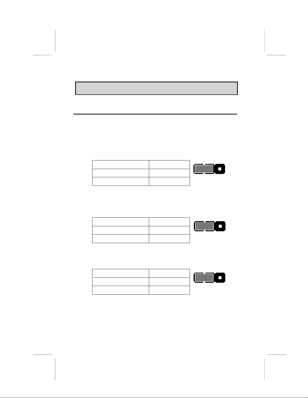
AAppppeennddiixx:: JJuummppeerr SSeettttiinngg RReeffeerreenncce
Quick Jumper Setting Reference
If you are familiar with most of the material in this chapter, you
can begin preparing the mainboard for installation by using this
quick reference to begin setting the jumpers.
JP1: Clear CMOS jumper
Use this jumper to clear the contents of the CMOS memory.
e
Function Jumper Setting
Normal operation Short pins 1-2
Clear CMOS Short pins 2-3
JP5: Suspend to RAM support enable/disable jumper
Use this jumper to enable or disable the Suspend to RAM (STR)
Function. You must also enable this function in the BIOS Setup
Utility. Refer to Chapter 3.
Function Jumper Setting
Enable Short pins 1-2
Disable Short pins 2-3
JP6: USB1 wake up jumper
Use this jumper to enabl e a signal to the USB port s (locat ed on the
I/O port panel) to wake up th e system fro m power saving mode.
Function Jumper Setting
Disable Short pins 1-2
Enable Short pins 2-3
1 2 3
1 2 3
1 2 3
JP1
JP5
JP6
75
Page 82

JP7: CPU frequency select jumper
Use this jumper to force a CPU that has a 66 MHz frontside bus
(FSB) to run at a 100 MHz FSB speed.
Function Jumper Setting
Normal operation Short pins 1-2
Force a 66 MHz FSB to
run at 100 MHz FSB
Short pins 2-3
1 2 3
Note: The CPU speed is determined by the CPU Host/PCI Clock
speed multiplied by the CPU Clock Ratio. Refer to the Frequency
Control Option in Chapter 3 for more information.
Forcing the CPU to run at a higher clock speed then it was rated
for is called overclocking and is not recommended.
JP8: CPU frequency select jumper
Use this jumper to force a CPU that has a 100 MHz frontside
bus (FSB) to run at a 133 MHz FSB speed.
Function Jumper Setting
Normal operation Short pins 1-2
Force a 100 MHz FSB to
run at 133 MHz FSB
Short pins 2-3
1 2 3
JP1
JP2
Note: The CPU speed is determined by the CPU Host/PCI Clock
speed multiplied by the CPU Clock Ratio. Refer to the Frequency
Control Option in Chapter 3 for more information.
Forcing the CPU to run at a higher clock speed then it was rated
for is called overclocking and is not recommended.
JP14: Onboard CODEC/AMR slot select jumper
Use this jumper to enable either the onboard codec or the AMR
slot (AMR1).
Function Jumper Setting
Onboard codec Short pins 1-2
AMR slot Short pins 2-3
1 2 3
76
JP14
Page 83

JP16: Dual color LED header
This header allows the user to install red and green LED indicators to indicate when the computer is in Suspend to RAM (STR)
or normal. Although the values are not predefined, red usually
indicates STR and green indicates nor mal.
JP17: USB2 wake up jumper
Use this jumper to enable a signal to the USB devices 3 and 4
(located on the front panel) to wake up the system from power
saving mode.
Function Jumper Setting
Disable Short pins 1-2
Enable Short pins 2-3
1 2 3
JP17
JP18: BIOS Flash protect jumper
Use this jumper to enable or disable the BIOS flash protection
on the mainboard. You should disable this jumper when you
want to flash the BIOS.
Function Jumper Setting
Disable Short pins 1-2
Enable Short pins 2-3
1 2 3
JP18
JP19: AMR codec mode
Use this jumper to define the AMR codec mode and avoid conflict with the onboard AC 97 codec.
Function Jumper Setting
Slave AMR card Short pins 1-2
Master AMR card Short pins 2-3
1 2 3
JP19
77
Page 84

PANEL1: Panel connectors for switches and indicators
Use the panel connector to implement the switches and indicators on your system case.
Panel connectors for switches and indicators
Function Pins
PANEL1
Power switch +22, 23
Hard disk LED Indicator +20, 21
Empty pin 19
23
Power Sw itch 22-23
HDD LED 20-21
Speaker +15, 16, 17, 18
Empty pin 14
Reset switch 12, 13
Speaker 15-16-17 -18
Empty pins 10, 11
Green LED indicator +7, +8, 9
Reset Switch 12-13
Empty pin 6
Sleep switch 4, 5
Power LED indicator +1, +2, 3
Green LED 7-8-9
PANEL1
Sleep Switch 4-5
Power LED 1-2-3
1
Note: The plus sign (+) indicates a pin which must be connected
to a positive voltage.
78
 Loading...