

Page 1

Preface
Copyright
This publication, including all photographs, illustrations and software,
is protected under international copyright laws, with all rights reserved. Neither this manual, nor any of the material contained herein,
may be reproduced without written consent of the author.
Version 1.0
Disclaimer
The information in this document is subject to change without notice.
The manufacturer makes no representations or warranties with respect to the contents hereof and specifically disclaims any implied
warranties of merchantability or fitness for any particular purpose.
The manufacturer reserves the right to revise this publication and to
make changes from time to time in the content hereof without obligation of the manufacturer to notify any person of such revision or
changes.
Trademark Recognition
Microsoft, MS-DOS and Windows are registered trademarks of Microsoft Corp.
MMX, Pentium, Pentium-II, Pentium-III, Celeron are registered
trademarks of Intel Corporation.
Other product names used in this manual are the properties of their
respective owners and are acknowledged.
Page 2

Federal Communications Commission (FCC)
This equipment has been tested and found to comply with the limits
for a Class B digital device, pursuant to Part 15 of the FCC Rules.
These limits are designed to provide reasonable protection against
harmful interference in a residential installation. This equipment generates, uses, and can radiate radio frequency energy and, if not
installed and used in accordance with the instructions, may cause
harmful interference to radio communications. However, there is no
guarantee that interference will not occur in a particular installation. If
this equipment does cause harmful interference to radio or television
reception, which can be determined by turning the equipment off
and on, the user is encouraged to try to correct the interference by
one or more of the following measures:
− Reorient or relocate the receiving antenna.
− Increase the separation between the equipment and the
receiver.
− Connect the equipment onto an outlet on a circuit different
from that to which the receiver is connected.
− Consult the dealer or an experienced radio/TV technician
for help.
Shielded interconnect cables and a shielded AC power cable must
be employed with this equipment to ensure compliance with the pertinent RF emission limits governing this device. Changes or
modifications not expressly approved by the system's manufacturer
could void the user's authorit y to operate the equipment.
ii
Page 3

Declaration of Conformity
This device complies with part 15 of the FCC rules. Operation is
subject to the following conditions:
− This device may not cause harmful interference, and
− This device must accept any interference received, in-
cluding interference that may cause undesired operation.
Canadian Department of Communications
This class B digital apparatus meets all requirements of the Canadian Interference-causing Equipment Regulations.
Cet appareil numérique de la classe B respecte toutes les exigences
du Réglement sur le matériel brouilieur du Canada.
iii
Page 4

About the Manual
The manual consists of the following:
Chapter 1
Introducing the Mainboard
Chapter 2
Installing the Mainboard
Chapter 3
Using BIOS
Chapter 4
Using the Mainboard Software
Appendix A
Appendix
Setting
A
Jumpers
Describes features of the mainboard, and provides a shipping
checklist.
Go to
⇒
page 1
Describes installation of mainboard components.
Go to
⇒
page 9
Provides information on using
the BIOS Setup Utility.
Go to
⇒
page 35
Describes the mainboard software.
Go to
⇒
page 63
Provides a reference to the
jumpers on the mainboard.
Go to
⇒
page 67
iv
Page 5

T
AABBLLEE OOFF
T
CHAPTER 1 1
CHAPTER 2 9
CHAPTER 3 35
CHAPTER 4 63
APPENDIX A 67
C
OONNTTEENNTTS
C
S
v
Page 6

CChhaapptteerr 1
Introducing the Mainboard
1
IInnttrroodduuccttiioon
Congratulations on purchasing the MS7057CT mainboard.
The MS7057CT mainboard is an ATX mainboard that uses a
4-layer printed circuit board and measures 304.8 mm x 220
mm. The mainboard features a Socket 370 that accommodates the Intel Ce leron 533A CPU and Intel C eleron CPUs at
566 MHz and above. It also supports Pentium III proc essors
up to 133 MHz.
The MS7057CT incorp orates the Intel 815EP B-s tep chipset,
which combines support for SDRAM, ATA-100, and 4xAGP.
The 82801BA I/O controller hub makes a direct connection
between the graphics s ystem, the IDE controller, and the PCI
bus and uses accelerated hub architecture to double the
bandwidth between these components enabling more lifelike
audio and video. The 82801BA I/O controller hub inclu des an
integrated audio-codec controller th at lets th e processor more
effectively decode sound generated by the integrated audio
system.
CChheecckklliisst
Compare the mainboar d ’s p ackage contents with the f o llo win g
checklists:
n
t
Standard Items
• One mainboard
• One diskette drive ribbon cable and bracket
• One IDE drive ribbon cable and bracket
• One auto-install software support CD
• This user’s manual
Page 7

FFeeaattuurrees
s
Processor
Chipset
Memory
The MS7057CT mainboard uses a Socket 370 that
has the following features:
• Accommodates the Intel Celeron 533A CPU
and Celeron CPUs at 566 MHz and above
• Accommodates Intel Pentium III/Tualatin CPUs
that support a FSB of 100 or 133 MHz
The Intel 815EP B-step chipset is based on an innovative and scaleable architecture with proven
reliability and performance. A few of the chipset’s
advanced features are:
• 82815 Memory Controller Hub (MCH) built on
Intel Graphics Technology, featuring a backwards compatible unified graphics driver
• 82801BA I/O Controller Hub (ICH2) which de-
livers twice the I/O bandwidth as traditional
bridge architecture
• Two USB controllers double the bandwidth to
24 Mbps across four ports
• Integrated AC 97 audio that supports full sur-
round sound with up to 6 channels
• An ATA 100 interface on the chipset, which
helps boost system performance by providing a
high-speed connection to ATA 100 Hard Disk
Drives, delivering maximum sustained data
transfer rates of 100 MB/sec
Additional key features include support for 4 USB
ports, an AC 97 link for audio and modem, hardware monitoring, and ACPI/OnNow power
management.
Supports SDRAM up to 512 MB, uses a 3 piece
3.3V unbuffered 168 pin socket, accommodates 3
double sided DIMMs at 100 MHz system memory
bus, also supports 2 double sided or 3 single sided
DIMMs at 133 MHz system memory bus
2
Page 8

VGA
AC 97 Audio
Codec
Expansion
Options
Integrated I/O
BIOS
Firmware
The MS7057CT includes a 4xAGP slot that
provides four times the bandwidth of the original
AGP specification. AGP technology provides a direct connection between the graphics sub-system
and the processor so that the graphics do not have
to compete for processor time with other devices
on the PCI bus.
The AC 97 Audio codec is compliant with the AC
97 2.1 specification, supports 18-bit ADC (Analog
Digital Converter) and DAC (Digital Analog Converter) resolution as well as 18-bit stereo fullduplex codec with independent and variable sampling rates. Further features include support for
four analog line-level stereo inputs.
The mainboard comes with the following expansion
options:
• Six 32-bit PCI slots
• One 4xAGP slot
• One Communications Network Riser (CNR)
slot
• Two IDE channels and one floppy disk drive
interface
The MS7057CT supports Ultra DMA bus mastering
with transfer rates of 33/66/100 MB/sec.
The mainboard has a full set of I/O ports and connectors:
• Two PS/2 ports for mouse and keyboard
• Two serial ports
• One parallel port
• One MIDI/game port
• Two USB ports
• Audio jacks for microphone, line-in and line-out
This mainboard uses Award BIOS that ena bl es
users to configure many system features including
the following:
• Power management
• Wake-up alarms
• CPU parameters
• CPU and memory timing
The firmware can also be used to set parameters
for different processor clock speeds
3
Page 9
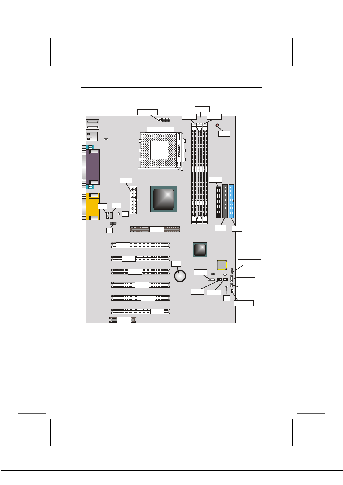
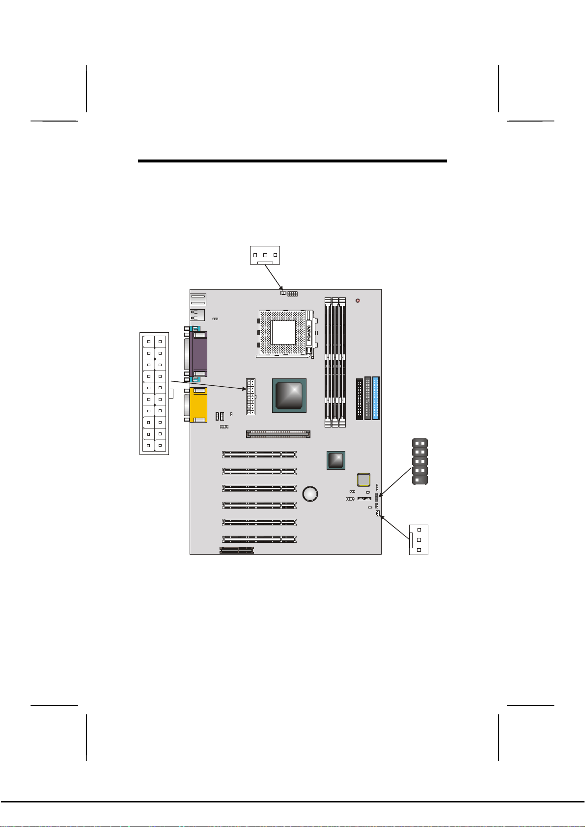
MMaaiinnbbooaarrdd CCoommppoonneenntts
CPUFAN1
CPUFAN1
1
JP3
ATX1
ATX1
ATX1
11111
CPUFAN1
JP12
CPU SOCKET
CPU SOCKET
s
JP9
JP8
JP11
JP10
DIMM1
DIMM1
DIMM2
DIMM2
DIMM3
DIMM3
LED1
FDD1
FDD1
LED1
LED1
CD1
CD1
CD2
CD2
CD1
CD2
J1
J1
J1
1
J3
J3
J3
PCI1
PCI1
PCI1
PCI2
PCI2
PCI2
PCI3
PCI3
PCI3
PCI4
PCI5
PCI6
CNR1
CNR1
CNR1
PCI4
PCI4
AGP1
PCI5
PCI5
AGP1
AGP1
PCI6
PCI6
BT1
BT1
BAT1
DIMM1 DIMM2
USB2
USB2
WOL1
WOL1
FDD1
DIMM3
JP1
1111
1111
USB2
WOM1
WOM1
IDE2
IDE2
WOL1 WOM1
IDE2
JP2
J4
J4
J4
IDE1
IDE1
IDE1
SPEAKER1
1111
1111
PANEL1
1111
SIR1
CASFAN1
CASFAN1
CASFAN1
SPEAKER1
SPEAKER1
PANEL1
PANEL1
SIR1
SIR1
4
Page 10

Table of Mainboard Components
Label Component
AGP1 Accelerated Graphics Port
ATX1 Power connector
BT1 Three volt realtime clock battery
CASFAN1 Auxiliary case cooling fan
CD1 Primary CD-in connector
CD2 Secondary CD-in connector
CNR1 Communications Networking Riser slot
CPU SOCKET Socket 370 for Intel Celeron and Pentium III
processors
CPUFAN1 Cooling fan for CPU
DIMM1 ~ DIMM3 Three 168-pin DIMM sockets
FDD1 Floppy disk drive connector
IDE 1 Primary IDE channel
IDE 2 Secondary IDE channel
J1 Case open alarm header
J3 Extra MIC/line-out header
J4 Sleep switch
1
LED1
PANEL1 Connector for case front panel switches and
PCI1 ~ PCI6 Six 32-bit add-on card slots
SIR1 Serial infrared cable header
SPEAKER1 Speaker connector
USB2 Front panel USB headers
WOL1 Wake On LAN wakeup connector
WOM1 Wake On Modem wakeup connector
Red 3 VSB LED for SDRAM
LED indicators
1
The red indicat or LED1 turns on if your system is s till powered, at which time memory modules cannot be installed or
uninstalled.
5
Page 11
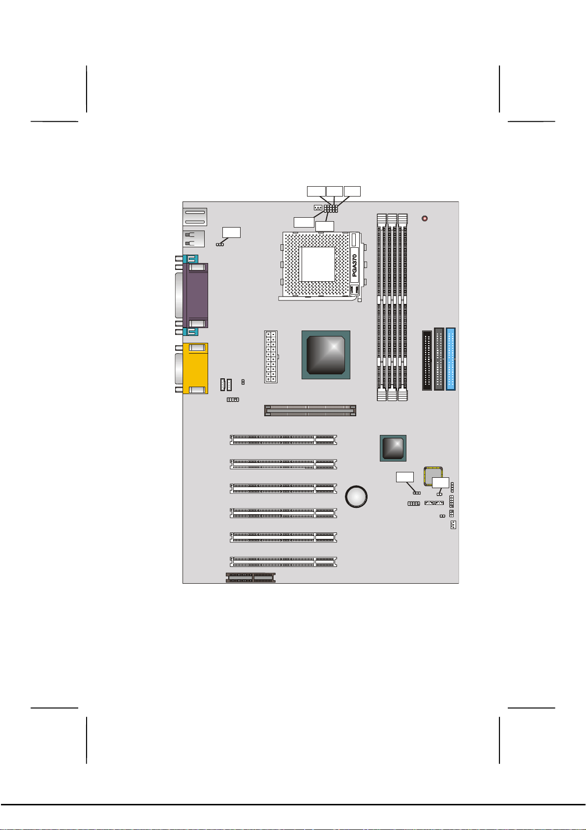
Jumpers
11111
JP11
JP9
JP11
JP12
JP8
JP1
LED1
FDD1
IDE1
JP1
JP2
WOL1 WOM1
IDE2
SPEAKER1
1111
1111
JP2
PANEL1
1111
SIR1
J4
CASFAN1
DIMM3
1111
1111
USB2
JP9
JP8
JP10
DIMM1 DIMM2
BAT1
JP10
CPUFAN1
JP12
JP3
1
JP3
ATX1
CD1
CD2
J1
1
J3
PCI1
PCI2
PCI3
PCI4
PCI5
AGP1
PCI6
CNR1
6
Page 12

Table of Jumpers
Label Component
JP1 Clear BIOS jumper
JP2 BIOS flash protection jumper
JP3 Keyboard power on jumper
JP8 – JP12 CPU core voltage jumpers
7
Page 13

CChhoooossiinngg aa CCoommppuutteerr CCaasse
There are many types of computer cas es on the market. T he
mainboard complies with the specifications for the ATX system case. Some f eatures on the mainb oard are implem ented
by cabling connectors on the mainboard to indicators and
switches on the s ystem case. Ensure that your case supports
all the features required. The mainboard can support one
floppy diskette drive and four enhanced IDE drives. Ensure
that your case has sufficient power and space for all the
drives that you intend to install.
Most cases have a choice of I/O tem plates in the rear panel.
Make sure that the I/O template in the case matches the I/O
ports installed on the rear edge of the mainboard.
This mainboard has an ATX form factor of 220 mm x 304.8
mm. Choose a case that accommodates this form factor.
This concludes Chapter 1. Chapter 2 explains how to install
the mainboard.
e
8
Page 14

CChhaapptteerr 2
Installing the Mainboard
2
SSaaffeettyy PPrreeccaauuttiioonns
Follow these safety precautions when installing the mainboard:
• Wear a grounding strip attached to a grounded device
to avoid damage from static electricity.
• Discharge static electricity by touching the metal case
of a safely grounded object before working on the
mainboard.
• Leave components in the static-proof bags they came
in.
• Hold all circuit boards by the edges. Do not bend cir-
cuit boards.
s
Page 15

QQuuiicckk GGuuiidde
This Quick Guide suggests the steps you can take to build
your system with the mainboards.
The following table describes installing specific components:
e
Locating Mainboard Components
Installing Jumpers
Installing the Mainboard in a Case
Installing Case Components
Installing the CPU
Installing Memory
Installing an HDD and CD-ROM Drive
Installing an FDD
Installing Add-on Cards
Connecting Options
Connecting Peripheral (I/O) Devices
The appendix provides a quick reference for jumper
Note:
settings.
Go to page 4
Go to page 11
Go to page 16
Go to page 17
Go to page 19
Go to page 22
Go to page 24
Go to page 27
Go to page 28
Go to page 30
Go to page 33
10
Page 16
CChheecckkiinngg JJuummppeerr SSeettttiinnggs
This section explains how to set jumpers for correct configuration of the mainboard.
s
Setting Jumpers
Use the mainboard jumpers to set system configuration options. Jumpers with m ore than one pin are num bered. When
setting the jumpers, ensure that the jumper caps are placed
on the correct pins.
This illustration shows a 2-pin
jumper. When the jumper cap is
placed on both pins, the jumper is
SHORT. If you remove the jumper
cap, or place the jumper cap on
Short Open
just one pin, the jumper is OPEN.
This illustration shows a 3-pin
jumper. Pins 1 and 2 are SHORT.
1
2
3
11
Page 17
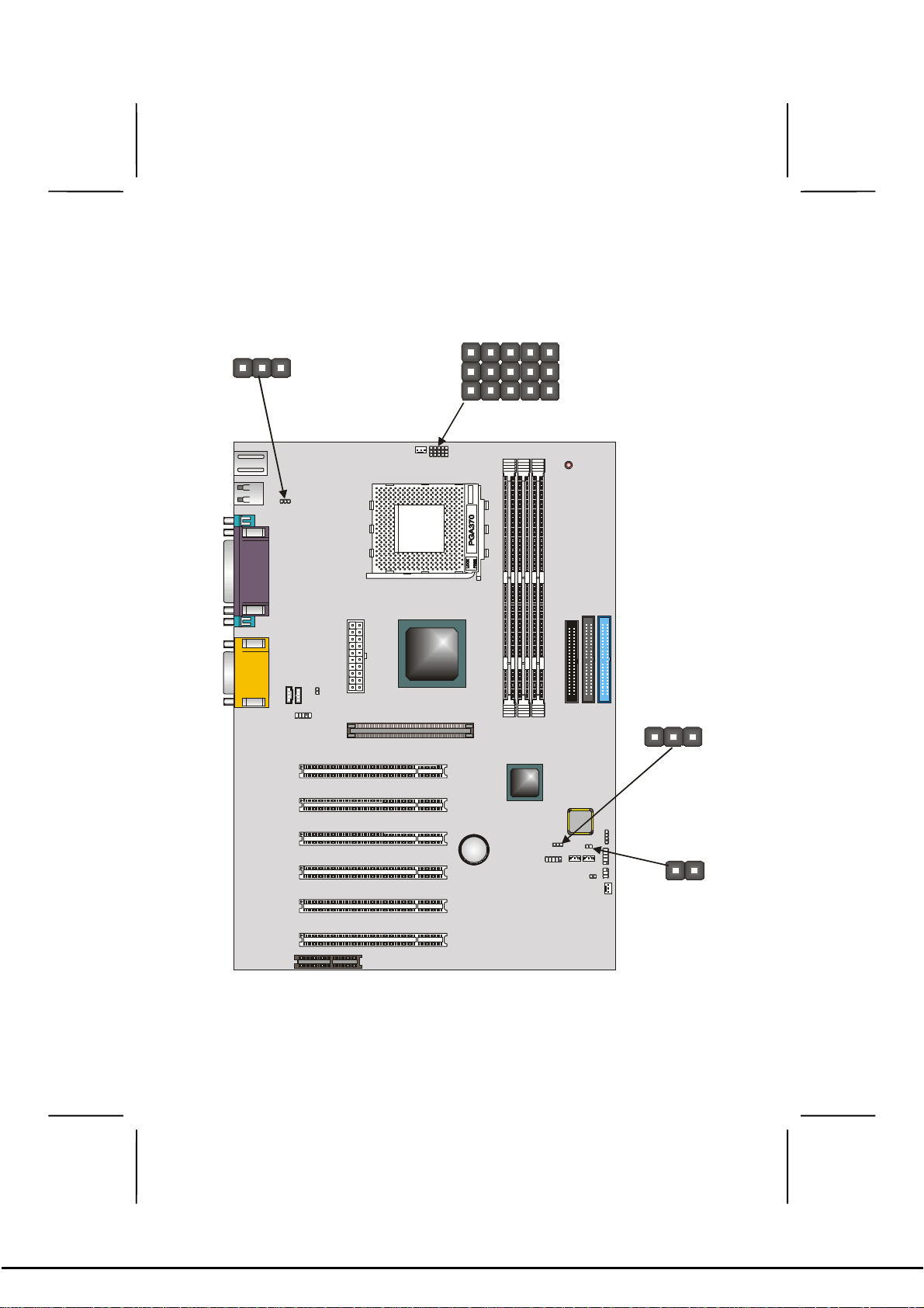
Checking Jumper Settings
In the following illustration, pin 1 is shown.
1
JP3
11111
JP9
DIMM3
JP8
LED1
FDD1
IDE1
IDE2
JP1
JP12
JP11
11111
CPUFAN1
JP9
JP8
JP11
JP12
JP10
1
JP3
ATX1
CD1
CD2
J1
1
J3
AGP1
JP10
DIMM1 DIMM2
1111
PCI1
PCI2
PCI3
PCI4
PCI5
PCI6
CNR1
BAT1
JP1
1111
1111
USB2
WOL1 WOM1
SPEAKER1
1111
1111
JP2
PANEL1
1111
SIR1
J4
CASFAN1
JP2
12
Page 18
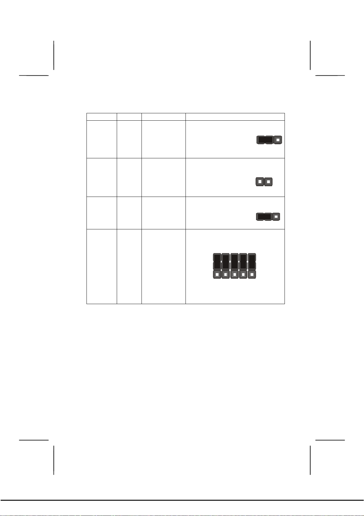
Jumper Settings
V
Jumper Type Description Setting (
JP1 3 pin Clear CMOS
JP2 2 pin BIOS flash
protection
JP3 3 pin KB power on
JP8
JP9
JP10
JP11
JP12
3 pin CPU core
voltage select
1-2: Normal
2-3: Clear CMOS
Open: Unlock
Short: Lock
1-2: Enable
2-3:Disable
ID25mv
(JP12)
1
Refer to the table on page 15 for
pin information.
default
1
1
VID0
(JP8)
)
JP1
JP2
JP3
13
Page 19

Jumper 1
1. Turn the system off.
2. Short pins 2 and 3 on jumper 1.
3. Return the jumper to the normal setting.
4. Turn the system on. The BIOS is returned to the de-
Jumper 2
from being updated (f lashed). Set th e jumper to unlock to update your BIOS. After updating the BIOS, change it to the
locked setting. For instructions on updating, the BIO S refer to
Chapter 3.
– This jumper enables you to clear the BIOS:
fault settings.
– This jumper enables you to prevent the BIOS
Jumper 3
power saving mode upon any keyboard activity.
Jumper 8 ~ Jumper 12
manually set the CPU core voltage.
Refer to the table on the next page for pin information.
– This jumper allo ws t he system to be awak en f r om
–Use these 3 x 5 pin jumpers to
14
Page 20

Jumper 8 – 12 pin settings
Pin Settings
Volt. VID0 VID1 VID2 VID3 VID25mv
Auto* 1-2 1-2 1-2 1-2 1-2
1.050V 2-3 2-3 Open 2-3 2-3
1.075V 2-3 2-3 Open 2-3 Open
1.100V Open Open 2-3 2-3 2-3
1.125V Open Open 2-3 2-3 Open
1.150V 2-3 Open 2-3 2-3 2-3
1.175V 2-3 Open 2-3 2-3 Open
1.200V Open 2-3 2-3 2-3 2-3
1.225V Open 2-3 2-3 2-3 Open
1.250V 2-3 2-3 2-3 2-3 2-3
1.275V 2-3 2-3 2-3 2-3 Open
1.300V Open Open Open Open 2-3
1.325V Open Open Open Open Open
1.350V 2-3 Open Open Open 2-3
1.375V 2-3 Open Open Open Open
1.400V Open 2-3 Open Open 2-3
1.425V Open 2-3 Open Open Open
1.450V 2-3 2-3 Open Open 2-3
1.475V 2-3 2-3 Open Open Open
1.500V Open Open 2-3 Open 2-3
1.525V Open Open 2-3 Open Open
1.550V 2-3 Open 2-3 Open 2-3
1.575V 2-3 Open 2-3 Open Open
1.600V Open 2-3 2-3 Open 2-3
1.625V Open 2-3 2-3 Open Open
1.650V 2-3 2-3 2-3 Open 2-3
1.675V 2-3 2-3 2-3 Open Open
1.700V Open Open Open 2-3 2-3
1.725V Open Open Open 2-3 Open
1.750V 2-3 Open Open 2-3 2-3
1.775V 2-3 Open Open 2-3 Open
1.800V Open 2-3 Open 2-3 2-3
1.825V Open 2-3 Open 2-3 Open
*Auto: When all 1-2 pins are shorted, the core voltage will automatically be determined.
These values are for reference only. It is not recommend-
Note:
ed to change the settings for jumper 8 ~ 12. Please notice
that the CPU will burn out if the core voltage is higher
than the default value.
15
Page 21

IInnssttaalllliinngg tthhee MMaaiinnbbooaarrdd iinn aa CCaasse
Refer to the following illus tration and instructions for installing
the mainboard in a case:
e
This illustration shows
an example of a mainboard being installed in
a tower-type case:
Do not over-
Note:
tighten the
screws as this
can stress the
mainboard.
Most system cases have
mounting brackets installed in the case,
which correspond to the
holes in the mainboard.
Place the mainboard
over the mounting
brackets and secure the
mainboard into the
mounting brackets with
screws.
The mainboard has a set of I/O ports on the rear edge. Ensure that your case has an I/O template that supports the I /O
ports and expansion slots.
2. Secure the screws in the
mainboard holes that align
with the chassis holes
1. Place the mainboard
over the case fasteners
16
Page 22
C
CCoonnnneeccttiinngg CCaassee CCoommppoonneenntts
s
After you have installed the m ainboard into a case, you can
begin connecting the mainboard components. Refer to the
following:
PUFAN1
11111
ATX1
CPUFAN1
JP9
JP8
JP11
JP12
JP10
1
JP3
ATX1
LED1
CD1
CD2
J1
1
J3
PCI1
PCI2
PCI3
PCI4
PCI5
PCI6
CNR1
AGP1
DIMM1 DIMM2
BAT1
FDD1
IDE1
IDE2
DIMM3
PANEL1
1111
SPEAKER1
JP1
1111
1111
1111
JP2
WOL1 WOM1
PANE L 1
1111
SIR1
J4
CASFAN1
CASFAN1
1111
USB2
1. Connect the case power supply connector to ATX1.
2. Connect the CPU cooling fan cable to CPUFAN1.
3. Connect the case cooling fan connector to CASFAN1
The following page explains how to make panel connections.
17
Page 23
The Panel Connector
The panel connector provides a standard set of switch and
LED connectors usually found on ATX or micro-ATX cases.
Refer to the table below for information:
Device Pins
HDD LED +1, -3
Green LED
+2, -4
Indicator
Reset
5, 7
Switch
Power
6, 8
ON/OFF
N/C 9
Empty 10
The plus sign (+ ) indicates a pin which must be con-
Note:
nected to a positive voltage.
HDD LED
(Pins 1, 3)
Reset Switch
(Pins 5, 7)
N/C
(Pin 9)
1 2
9 10
Green LED
(Pins 2, 4)
Power Switch
(Pins 6, 8)
Empty
(Pin 10)
18
Page 24

IInnssttaalllliinngg HHaarrddwwaarre
e
Installing the Processor
Caution:
make sure that you DO NOT scratch the mainboard or any
of the surface-mount resistors with the clip of the cooling
fan. If the clip of the cooling fan scrapes across the mainboard, you may cause serious damage to both the
mainboard and the processor.
On most mainboards, there are small surface-mount resistors near the processor socket, which may be damaged if
the cooling fan is carelessly install ed.
Avoid using cooling fans with sharp edges on the fan casing
and the clips. Also, install the cooling fan in a well-lit work
area so that you can clearly see the mainboard and processor socket .
When installing a CPU heatsink and cooling fan
Before installing the Processor
This mainboard autom atically determines the CPU clock frequency and system bus fr equency for processor. You ma y be
able to change thes e automatic settings by making changes
to jumpers on the m ainboard, or changing the settings in the
system Setup Utilit y. We strongly recomm end that you do not
overclock the mainboard to run processors or other components faster than their rated speed.
Warning:
the reliability of the system and introduce errors into your
system. Overclocking can permanently damage the mainboard by generating excess heat in components that are
run beyond the rated limits.
Overclocking components can adversely affect
This mainboard has a Socket 370 processor socket. When
choosing a process or, consider the perf ormanc e requirem ents
of the system. Per f orm anc e is bas ed on the processor desi gn,
the clock speed and system bus frequency of the processor,
and the quantity of inter nal cach e m em ory and ex terna l c ache
memory.
19
Page 25

CPU Installation Procedure
The following illustration shows CPU installation components:
Socket 370
CPU fan
Pin-1 corner
Locking lever
20
Page 26

Follow these instructions to install the CPU:
1. Pull the CPU socket locking lever away from the sock-
2. Identify the pin-1 corner on the CPU socket and the
3. Match the pin-1 corners and insert the processor into
CPU fan and
CPU fan and
heatsink assembly
heatsink assembly
et to unhook it and raise the locking lever to the upright
position.
pin-1 corner on the processor.
the socket. Do not use force.
CPU fan connector
CPU fan connector
CPUFAN1
CPUFAN1
Locking lever
Locking lever
Pin-1 corners
Pin-1 corners
4. Swing the locking lever down and hook it under the
latch on the edge of the socket.
5. Plug the CPU fan power cable into the CPU cooling
fan power supply on the mainboard (CPUFAN1).
After you have assembled the system, yo u must set
Note:
the correct clock speed and frontside bus (FSB)
speed. Check the jumper section in Appendix A and
refer to Chapter 3 “Frequency Voltage Control” for
more information.
21
Page 27

Install Memor y Modules
For this mainboard, you
must use 168-pin 3.3V
non-buffered Dual In-line
Memory Modules
(DIMMs). The memory
chips are standard
SDRAM (Sync hrono us
Dynamic Random Access Memory). The table
at the right shows the
supported frequen cies.
Frontside Bus
(FSB)
Frequency
66 MHz 100 MHz
100 MHz 100 MHz
133 MHz 100 MHz
133 MHz 133 MHz
Note:
The memory bus runs at either
100 MHz or 133 MHz independent of
the system bus frequency.
System Memory
Bus (SMB)
Frequency
Installation Procedure
The mainboard accommodates three memory modules. You
must install at le ast one module in an y of the thr ee s lots. Each
module can be installed with 32 MB to 512 MB of memory;
total memory capacity is 512 MB.
1. Align the memory module with the slot. The DIMM
slots are keyed with notches and the DIMMs are keyed
22
Page 28

with cutouts so that they can only be installed correctly.
Check that the cutouts on the DIMM module edge
connector match the notches in the DIMM slot:
Latch
Notches
Cutouts
Latch
2. Push the latches on each side of the DIMM slot down.
3. Install the DIMM module into the slot and press it firmly
down so that it seats correctly. The slot latches are
levered upwards and latch on to the edges of the
DIMM when it is installed correctly.
23
Page 29

Installing a Hard Disk Drive/CD-ROM
This section describes how to install IDE devices such as a
hard disk drive and a CD-ROM drive.
About IDE Devices
Your mainboard has a primary and secondary IDE channel interface (IDE1 and IDE2 ). An IDE ribbon cabl e suppor ting two IDE
devices is bundled with the mainboard. IDE devices have jumpers or switches that are used to set the IDE device as MASTER
or SLAVE. Refer to the IDE device user’s manual.
If you want to install m or e than two I DE de vices, get a se cond
IDE cable and you can add two more devices to the secondary IDE channel.
When installing two IDE devices on one cable, ensure that
one device is set to MAST ER and the other device is set to
SLAVE. The documentation of your IDE device explains how
to do this.
About UDMA
This mainboard su pports UltraDMA 66/ 100. UDMA is a technology that accelerates t he perform ance of devices in the IDE
channel. Install IDE d evices that support UD MA and use IDE
cables that support UDMA for better performance.
24
Page 30

Installing a Hard Disk Drive
1. Install the hard disk drive into the drive cage in your
ATX system case.
2. Plug the IDE cable into IDE1 (A):
HDD
B
C
A
Ribbon cable connectors are usually keyed so that
Note:
they can only be installed correctly on the device
connector. If the connector is not keyed, make sure
that you match the pin-1 side of the cable connector
with the pin-1 side of the device connector. Each
connector has the pin-1 side clearly marked. The
pin-1 side of each ribbon cable is always marked
with a colored stripe on the cable.
3. Plug an IDE cable connector into the hard disk drive
IDE connector (B). It doesn't matter which connector
on the cable you use.
4. Plug a power cable from the case power supply into
the power connector on the hard disk drive (C).
When you first start up your system, the BIOS should automatically detect your hard disk drive. If it doesn’t, enter the
Setup Utility and use the IDE Har d D isk Auto Detect feature to
configure the hard disk drive that you have installed. See
Chapter 3 for more information.
25
Page 31

Installing a CD-ROM/DVD Drive
1. Install the CD-ROM/DVD drive into the drive cage in
your ATX system case.
2. Plug the IDE cable into IDE1 (A). If you have already
installed an HDD, you can use the free connector on
its IDE cable.
CD-ROM audio
CD-ROM
connector
CD2
D
Ribbon cable connectors are usually keyed so that
Note:
they can only be installed correctly on the device
connector. If the connector is not keyed, make sure
that you match the pin-1 side of the cable connector
with the pin-1 side of the device connector. Each
connector has the pin-1 side clearly marked. The
pin-1 side of each ribbon cable is always marked
with a colored stripe on the cable.
CD1
B
C
A
3. Plug an IDE cable connector into the CD-ROM/DVD
drive IDE connector (B). It doesn't matter which connector on the cable you use.
4. Plug a power cable from the case power supply into
the power connector on the CD-ROM/DVD drive (C).
26
Page 32

5. Use the audio cable provided with the CD-ROM/DVD
drive to connect to the mainboard CD-in connector
CD1 or CD2 (D).
When you first start up your system, the BIOS should automatically detect your CD-ROM/ DVD drive. If it doesn’t, enter
the Setup Utility and configure the CD-ROM/DVD drive that
you have installed. See Chapter 3 for more information.
Installing a Floppy Diskette Drive (FDD)
The mainboard has one floppy diskette drive interface (FDD1).
A diskette drive rib bon cable is shipp ed with the mother board.
Yo u can install a 5.25- inch drive or a 3.5- inch drive with various capacities. The flopp y diskette dr iv e cables ha ve one t ype
of connector for a 5.25-inch drive and another type of connector for a 3.5-inch drive
1. Install the FDD into the drive cage in your ATX system
case.
2. Plug the FDD cable into FDD1 (A):
FDD
B
Ribbon cable connectors are usually keyed so that
Note:
they can only be installed correctly on the device
connector. If the connector is not keyed, make sure
27
C
A
Page 33

that you match the pin-1 side of the cable connector
with the pin-1 side of the device connector. Each
connector has the pin-1 side clearly marked. The
pin-1 side of each ribbon cable is always marked
with a colored stripe on the cable.
3. Plug one of the connectors on the FDD cable into the
FDD connector (B).
4. Plug a power cable from the case power supply into
the power connector on the FDD (C).
When you first start up your system, go immediately to the
Setup Utility and use the Sta ndard page t o config ure the f loppy diskette drives that you have installed. See Chapt er 3 for
more information.
Installing Add-On Cards
This mainboard has six 32-bit PCI (Peripheral Components
Interconnect) expansion slots, one 4xAGP slot, and one
Communications and Networking Riser (CNR) slot.
PCI Slots
4xAGP Slot
CNR Slot
PCI slots are used to install expansion
cards that have the 32-bit PCI interface.
The 4xAGP slot is used to install a graphics adapter that supports the 4xAGP
specification and has a 4xAGP edge connector.
This slot is used to insert CNR cards including LAN, Modem, and Audio functions.
28
Page 34

F
AGP
CD1
CD2
J1
IDE1
IDE2
1
J3
PCI1
PCI2
AGP1
DIMM1 DIMM2
DIMM3
PCI
CNR
PCI3
PCI4
PCI5
PCI6
CNR1
Before installing an add-on card, check the docu-
Note:
BAT1
mentation for the card carefully. If the card is not
Plug and Play, yo u may ha ve to ma n ual l y con fi gur e
the card before installation.
1. Remove a blanking plate from the system case corresponding to the slot you are going to use.
2. Install the edge connector of the add-on card into the
expansion slot. Ensure that the edge connector is correctly seate d in the slot.
WOL1 WOM1
SPEAKER1
1111
1111
JP2
PANEL1
1111
SIR1
J4
CASFAN1
JP1
1111
1111
USB2
Edge connector
3. Secure the metal bracket of the card to the system
case with a screw.
For some add-on cards, for example graphics adapters
Note:
and network adapters, you have to install drivers and
software before you can begin using the add-on card.
29
Page 35

Connecting Optional Devices
US
Refer to the following for inf ormation on connectin g the mainboard’s optional device s:
11111
J1
CPUFAN1
JP9
JP8
JP11
JP12
JP10
1
JP3
ATX1
CD1
CD2
J1
1
J3
AGP1
DIMM1 DIMM2
LED1
FDD1
SPEAKER1
IDE1
IDE2
DIMM3
PCI1
PCI2
J3
PCI3
1111
PCI4
PCI5
PCI6
CNR1
BAT1
JP1
1111
WOL1 WOM1
1111
USB2
1111
SIR1
1111
SPEAKER1
1111
1111
JP2
PANEL 1
1111
SIR1
J4
J4
CASFAN1
1111
B2
WOL1
WOM1
30
Page 36

J1: Case open
This jumper prevents unauthorized access to your com puter
by enabling an alert alarm when the computer case is opened .
J3: Front panel MIC/line-out
This header allows the user to install auxiliary front-oriented
microphone and line-out ports for easier access.
Pin Signal Name Pin Signal Name
AUD_GND
AUD_MIC
1
AUD_MIC_BIAS
3
AUD_FPOUT_R
5
HP_ON
7
AUD_FPOUT_L
9
2
4
6
8
10
AUD_VCC
AUD_RET_R
KEY
AUD_RET_L
J4: Sleep Switch
This connector attac hes to a front pane l button used to leave
the system in a sleep state.
Pin Signal Name
1
Positive
2
Negative
SPEAKER1: Internal speaker
Connect the internal speaker connector to this header.
Pin Signal Name
1
SPKR
2
NC
3
Ground
4
+5V
WOL1/WOM: Wake On LAN/Wake On Modem
If you have installed a LAN card, use the c able provided with
the card to plug into t he m ainbo ard W O L1 connector. This enables the Wake On LAN (WOL) feature. W hen your s ystem is
in a power-saving mode, any LAN signal automatically resumes the system . You must enable this item us ing the Power
Management page of the Setup Utility.
31
Page 37

Pin Signal Name
1
5VSB
2
Ground
3
SENSE
If you have installed a modem, use the cable provided with
the modem to plug into th e mainboar d W OM1 connector. This
enables the Wake On Modem (WOM) feature. When your
system is in a power-saving mode, an y modem signal automatically resumes the system. You must enable this item
using the Power Managem ent page of the Setup Utility. See
Chapter 3 for more information.
SIR1: Serial infrared port
The mainboard supports a Serial Infrared (SIR) data port. Infrared ports allow the wireless exchange of information
between your computer and similarly equipped devic es. These devices may include printers, laptops, Personal Digital
Assistants (PDAs), and other computers.
Pin Signal Name Pin Signal Name
1
3
5
Not assigned
+5V
IRTX
2
4
6
(No Pin)
Ground
IRRX
USB2: USB port 3, 4
The mainboard has two USB ports installed on the rear edge
I/O port array. However, some computer cases have a sp ecial
module that mounts USB ports at the front of the cas e. If you
have this kind of case, use auxiliary USB connectors USB2
and USB3 to connect the front-mounted ports to the mainboard.
Pin Signal Name Pin Signal Name
VREG_FP_USBPWR0
VREG_FP_USBPWR0
1
USB_FP_P0-
3
USB_FP_P0+
5
Ground
7
Key
9
32
2
4
6
8
10
USB_FP_P1USB_FP_P1+
Ground
USB_FP-OC0
Page 38

CCoonnnneeccttiinngg II//OO DDeevviiccees
s
The backplane of the mainboard has a full set of I/O ports:
PS/2
mouse
PS/2
keyboard
USB
ports
Pa ra lle l port (LPT1)
Serial port
COM 1
Serial port
COM 2
Game port
Microphone
Line-in
Line-out
1. Use the upper PS/2 port to connect a PS/2 pointing
device. Use the lower PS/2 port to connect a PS/2
keyboard.
2. Use the USB ports to connect USB devices.
3. Use LPT1 to connect printers or other parallel communications devices.
4. Use the COM ports to connect serial devices such as
mice or fax/modems. COM1 is identified by the system
as COM1/3. COM2 is identified by the system as
COM2/4.
5. Use the game port to connect a joystick or a MIDI device.
6. Use the three audio ports to connect audio devices.
The left side jack is for a stereo line-out signal. The
middle jack is for a stereo line-in signal. The right side
jack is for a microphone.
33
Page 39

External Connector Color Coding
Many connectors now use standard colors as shown in the
table below.
Connector Color
Analog VGA Blue
Audio line in Light blue
Audio line out Lime
Digital monitor / flat panel White
IEEE 1394 Grey
Microphone Pink
MIDI/Game Gold
Parallel Burgundy
PS/2 compatible keyboard Purple
PS/2 compatible mouse Green
Serial Teal or Turquoise
Speaker out/subwoofer Orange
Right-to-left speaker Brown
USB Black
Video out Yellow
SCSI, network, telephone,
modem
None
This concludes Chapter 2. Chapter 3 covers the BIOS.
34
Page 40

CChhaapptteerr 3
Using BIOS
3
AAbboouutt tthhee SSeettuupp UUttiilliitty
The computer uses the latest Award BIOS with support for
Windows Plug and Play. The CMOS chip on the mainboard
contains the ROM setup instructions f or configuring th e mainboard BIOS.
The BIOS (Basic Input and Output System) Setup Uti lity displays the system's configuration status a nd provides you with
options to set system parameters. T he parameters are s tored
in battery-backed-up CMOS RAM that saves this inform ation
even when the power is turn ed off . W hen the system is turned
back on, the system is configured with the values found in
CMOS.
The BIOS Setup Utility enables you to configure:
• Hard drives, diskette drives, and peripherals
• Video display type and display options
• Password protection from unauthorized use
• Power management features
The settings made in the Se tup Uti li t y aff ect how th e computer
performs. Befor e using the Setup Utility, ensure that you understand the Setup Utility options. Only change settings
appropriate for the way you use the computer.
y
This chapter provides explanations for Setup Utility options.
Page 41

The Standard Configuration
A standard configuration has already been set in the Setup
Utility. However, we recommend that you read this chapt er in
case you need to make any changes in the future.
This Setu p Utility should be used:
• when changing the system configuration
• when a configuration error is detected and you are
prompted to make changes to the Setup Utility
• when trying to resolve IRQ conflicts
• when making changes to the Power Management con-
figuration
• when changing the password or making other changes
to the Security Setup
36
Page 42

Entering the Setup Utility
When you power on the s ystem, BIOS enters the P ower-On
Self Test (POST) r outines. POST is a series of bui lt-in diagnostics perform ed by the BIOS. After the POST routi nes are
completed, the following message appears:
Press DEL to enter SETUP
Pressing the delete ke y accesses the Award BIOS Setup
Utility:
CMOS Setup Utility – Copyright (C) 1984 – 2001 Award Software
Standard CMOS Features
Advanced BIO S Features
Advanced Chi pset Features
Integrated Peripherals
Power Management Setup
PnP/PCI Configurations
PC Health Stat us
Esc : Quit
F10 : Save & Exit Setup
Time, Date, Hard Disk Type . . .
Frequency/Voltage Contr ol
Load Fail-Safe Def aul ts
Load Optimized Defa ul ts
Set Supervisor Password
Set User Password
Save & Exit Setup
Exit Without Saving
↑↑↑↑ ↓↓↓↓ →→→→
←←←←
: Select Item
BIOS Navigation Keys
The BIOS navigation keys are listed below:
Key Function
Esc Exits the current menu
←↑↓→
+/–
/PU/PD
F10 Saves the current configuration and exits setup
F1
F5 Loads previously saved values to CMOS
F6 Loads a minimum configuration for trouble-
F7 Loads an optimum set of values for peak per-
Scrolls through the items on a menu
Modifies the selected field's values
Displays a screen that describes all key functions
shooting.
formance
37
Page 43

Updating the BIOS
You can download and install updated BIOS for this mainboard from the manufac turer's web site. New BIOS provides
support for new peripher als, im provem ents in perf orm ance, or
fixes for known bugs. Install new BIOS as follows:
1. If your mainboard has a BIOS protection jumper,
change the setting to allow BIOS flashing. Refer to
Appendix A for jumper settings.
2. If your mainboard has an item called Firmware Write
Protect in Advanced BIOS features, disable it. Firmware Write Protect prevents BIOS from being
overwritten.
3. Create a bootable system disk. Refer to Windows online help for information on creating a bootable system
disk.
4. Download the Flash Utility and new BIOS file from the
manufacturer's Web site. Copy these files to the system diskette you created in Step 3.
5. Turn off your computer and insert the system diske tte in
your computer's di skette driv e. You migh t need to run the
Setup Utility and change the boot pri ority items on the
Advanced BIOS Featu r e s Setu p pag e, to fo rce y ou r
computer to boot fro m the floppy diskette drive fi rst.
6. At the A:\ prompt, type the Flash Utility program name
and press <Enter>. You see a screen similar to the
following:
(C) Award Software 1999 All Rights Reserved
For (MAINBOARD NAME) DATE: 10/26/2000
Flash Type
File Name to Program :____________________
Error Message
FLASH MEMORY WRITER V7.33
7. Type the filename of the new BIOS in the “File Name
to Program” text box. Follow the onscreen directions to
update the mainboard BIOS.
8. When the installation is complete, remove the floppy
diskette from the diskette drive and restart your computer. If your mainboard has a Flash BIOS jumper,
reset the jumper to protect the newly installed BIOS
from being overwritten.
38
Page 44

UUssiinngg BBIIOOS
When you start the Setup Uti lity, the main menu appears. The
main menu of the Setup Utility displays a list of the options
that are available. A highlight indicates which option is currently selected. Use the cursor arrow keys to move the
highlight to other opt ions. When an option is highlig hted, execute the option by pressing <Enter>.
Some options lead to pop- up dialog boxes tha t prompt you to
verify that you wish to exec ute that opt ion. Oth er options lead
to dialog boxes prompt you for information.
S
Some options (marked with a triangle
that enable you to change the values for the option. Use the
cursor arrow keys to scroll through the items in the submenu.
In this manual, default values are enclosed in parenthesis.
Sub-menu items are denoted by a triangle
) lead to submenus
.
39
Page 45

Standard CMOS Features
This option displays a tab le of item s defining basic i nfor m ation
about your system.
CMOS Setup Utility – Copyright (C) 1984 – 2001 Award Software
Date (mm:dd:yy) Tue, July 11 2001
Time (hh:mm:ss) 12 : 8 : 59
IDE Primary Master
IDE Primary Slave
IDE Secondar y Master
IDE Secondary Slave
Drive A [1.44M, 3.5 in.]
Drive B [None]
Floppy 3 Mode Support [Disabled]
Video [EGA/VGA]
Halt On [All Errors]
Base Memory 640K
Extended Memory 31744K
Total Memory 32768K
↑↑↑↑ ↓↓↓↓ →→→→ ←←←←
: Move Enter : Select +/-/PU/PD:Value: F10: Save ESC: Exit F1:General Help
F5:Previous Values F6:Fail-Safe Defaults F7:Optimized Defaults
Date and Time
The Date and Time items show the curren t date and time on
the computer. If you are running a Windows OS, these items
are automaticall y upda ted wh e ne ver you make changes to the
Windows Date and Time Properties utility.
Standard CMOS Features
Menu Level
Change the da y, month,
year and century.
Item Help
IDE Devices (None)
Your computer has two IDE channels (Primary and Secondary)
and each channel can be installed with one or two devices
(Master and Slave). Use these it ems to configure eac h device
on the IDE channel.
40
Page 46

Press <Enter> to display the IDE sub-menu:
CMOS Setup Utility – Copyright © 1984 – 2001 Award Software
IDE HDD Auto-Detection Press Enter
IDE Primary Master [Auto]
Access Mode [Auto]
Capacity 0 MB
Cylinder 0
Head 0
Precomp 0
Landing Zone 0
Sector 0
↑↑↑↑ ↓↓↓↓ →→→→ ←←←←
: Move Enter : Select +/-/PU/PD:Value: F10: Save ESC: Exit F1:General Help
F5:Previous Values F6:Fail-Safe Defaults F7:Optimized Defaults
IDE Primary Master
Menu Level
To auto-detect the
HDD’s size, head . . . on
this channel
IDE HDD Auto-Detection
Press <Enter> while th is it em is high lighte d to pr om pt the Setup Utility to automatic ally detect and configure an ID E device
on the IDE channel.
If you are setting up a new hard disk drive that sup-
Note:
ports LBA mode, more than one line will appear in
the parameter box. Choose the line that lists LBA
for an LBA drive.
Item Help
IDE Primary/Secondary Master/Slave (Auto)
Leave this item at Auto to enable the system to automatically
detect and c onf ig ur e IDE dev ic es on th e ch ann el. If it f ails to f ind
a device, change the value to Manual and then manually configure the drive by entering the characteristics of the drive in the
items described below.
Refer to your drive's docum ent at i on or look on t h e drive cas i n g if
you need to obtain this information. If no device is installed,
change the value to None.
Before attempting to configure a hard disk drive,
Note:
ensure that you have the configuration infor mation
supplied by the manufacturer of your hard drive. Incorrect settings can result in your system not
recognizing the installe d hard disk.
41
Page 47

Access Mode
This item defines ways that can be used to access IDE hard
disks such as LBA (Large Block Addressing). L ea ve t his value
at Auto and the system will automatically decide the fastest
way to access the hard disk drive.
Press <Esc> to return to the Standard CMOS Features page.
Drive A/Drive B (1.44M, 3.5 in./None)
These items define the characteristics of any diskette drive
attached to the system . You can con nect one or two diskette
drives.
Floppy 3 Mode Support (Disabled)
Floppy 3 mode refer s to a 3.5-inch diskette with a c apacity of
1.2 MB. Floppy 3 mode is sometimes used in Japan.
Video (EGA/VGA)
This item defines the video mode of the system. T his mainboard has a built-in VG A gr a ph ics s ystem; you must leave this
item at the default value.
Halt On (All Errors)
This item defines the operation of the system POST (Power
On Self Test) routine. You can use this item to select which
types of errors in the POST are sufficient to halt the system.
Base Memory, Extended Memory, and Total Memory
These items are autom atically detecte d by the s ystem at star t
up time. These are display-only fields. You cannot make
changes to these fields.
42
Page 48

Advanced BIOS Setup Option
This option displa ys a table of items that define advanced information about your system.
CMOS Setup Utility – Copyright (C) 1984 – 2001 Award Software
Anti-Virus Protection [Disabled]
CPU Internal C ache [Enabl ed]
External Cache [Enabled]
CPU L2 Cache ECC Checking [Enabled]
Processor Number Feature [Enabled]
Quick Power On Self Test [Enabled]
First Boot Device [Floppy]
Second Boot D evice [HDD-0]
Third Boot Device [LS120]
Boot Other Device [Enabled]
Swap Floppy Drive [Disabled]
Boot Up Floppy Seek [Enabled]
Boot Up NumLock Statu s [On]
Gate A20 Option [Fast]
Typematic Rate Setting [Disabled]
x Typematic Rate (Chars/Sec) 6
x Typematic Delay (Msec) 250
Security Option [Setup]
OS Select For DRAM > 64MB [Non-OS2]
↑↑↑↑ ↓↓↓↓ →→→→ ←←←←
: Move Enter : Select +/-/PU/PD:Value: F10: Save ESC: Exit F1:General Help
F5:Previous Values F6:Fail-Safe Defaults F7:Optimized Defaults
Anti-Virus Protection (Disabled)
When enabled, this item provides protection against viruses
that try to write to the boot sector and partit ion table of your
hard disk drive. You need to disable this item when installing
an operating system. We recommend that you enable antivirus protection as soon as you have installed an operating
system.
Advanced BIO S Features
Menu Level
Allows you to choose
the VIRUS warni ng
feature for IDE Hard
Disk boot sector
protection. If this
function is enabled
and someone attempts
to write data into this
area, BIOS will show a
warning message on
screen and alarm beep
Item Help
CPU Internal Cache CPU Internal Cache (Enabled)
All processors that can be installed in th is mainboard use internal level 1 (L1) cache memory to improve performance.
Leave this item at the default value for better performance.
43
Page 49

External Cache (Enabled)
Most processors that can be installed in this system us e external level 2 (L2) cache memory to improve performance.
Leave this item at the default value for better performance.
CPU L2 Cache ECC Checking (Enabled)
This item enables or disables ECC (Error Correction Code) error checking on the CPU cache m emory. We recommend that
you leave this item at the default value.
Processor Number Feature (Enabled)
Some new processors are installed with a unique processor
number. This number may be used for verificat ion in Internet
transactions and e-com merce. If you prefer not to use or distribute the unique processor number, disable this item to
suppress the processor number.
Quick Power On Self Test (Enabled)
Enable this item to shorten the power on testing (POST) and
have your system start up faster. You might like to enable this
item after you are confide nt that your system hardware is operating smoothly.
1st/2nd/3rd Boot Device (Floppy/HDD-0/LS120)
Use these three items to select the priority and order of the
devices that your system searches for an operating s ystem at
start-up time.
Boot Other Device (Enabled)
When enabled, the system searches all other possible locations for an operating system. If it fails to find one in the
devices specified under the first, second, and third boot devices.
Swap Floppy Drive (Disabled)
If you have two flopp y disk ette drives i n your s ystem , this item
allows you to swap the ass igned drive letters so that drive A
becomes drive B, and drive B becomes drive A.
44
Page 50

Boot Up Floppy Seek (Enabled)
If this item is enabled, it checks the size of the floppy disk
drives at start-up time. You don't need to enable this item unless you have a legacy diskette drive with 360K capacity.
Boot Up NumLock Status (On)
This item defines if the keyboard Num Lock key is active when
your system is started.
Gate A20 Option (Fast)
This item defines how the system handles legacy software
that was written for an ear lier g eneratio n of process ors. Le ave
this item at the default value.
Typematic Rate Setting (Disabled)
If this item is enabled, you can use the following two items to
set the typematic rate and the typematic delay settings for
your keyboard.
Typematic Rate (Chars/Sec):
•
how many characters per second are generated by a
held-down key.
Typematic Delay (Msec):
•
many milliseconds must elapse before a held-down
key begins generating repeat characters.
Use this item to define
Use this item to define how
Security Option (Setup)
If you have installe d password protection, this it em defines if
the password is require d at system star t up, or if it is onl y required when a user tries to enter the Setup Utility.
OS Select For DRAM > 64 MB (Non-OS2)
This item is only requir ed if you have installed more than 64
MB of memory and you are runni ng the OS/2 operating system. Otherwise, leave this item at the default.
HDD S.M.A.R.T Capability (Disabled)
The S.M.A.R.T. (Self-Monitoring, Analysis, and Reporting
Tec hnology) system is a diagnos tics technology tha t monitors
and predicts device per form ance. S.M.A.R.T. software resides
on both the disk drive and the host computer.
45
Page 51

The disk drive sof tware monitors the internal perf ormance of
the motors, media, heads, and electronics of the drive. The
host software monitors the overall reliability status of the drive.
If a device failure is predicted, the host software, through the
Client WORKS S.M.A.R.T applet, warns the user of the impending condition and advises appropriate action to protect
the data.
Report No FDD For WIN95 (Yes)
If you are running a system with no floppy drive and using
Windows 95, select Yes for this item to ensure compatibility
with the Windows 95 logo certification. Otherwise, select No.
Advanced Chipset Features Option
This option displa ys a table of items that def ine critical tim ing
parameters of the mainboard. You should leave the items on
this page at their def ault values unless you are ver y familiar
with the technical specifications of your system hardware. If
you change the va lues incorrec tly, you may introduce fatal errors or recurring instability into your system.
CMOS Setup Utility – Copyright (C) 1984 – 2001 Award Software
SDRAM CAS Latency Time [3]
SDRAM Cycle Time Tras/TRC [7/9]
SDRAM RAS-to- CAS Delay [3]
SDRAM RAS Prec harge Time [3]
System BIOS Cacheable [Enabled]
Video RAM Cacheable [ Enabled]
Memory Hole At 15M-16M [Disabled]
CPU Latency Timer [Enabled]
Delayed Transaction [Enabled]
AGP Graphics Apert ure Si ze [64MB]
AGP Device 4X S upport [Enabled]
System Memory Frequency [100MHz]
Advanced Chi pset Features
Item Help
Menu Level
↑↑↑↑ ↓↓↓↓ →→→→ ←←←←
: Move Enter : Select +/-/PU/PD:Value: F10: Save ESC: Exit F1:General Help
F5:Previous Values F6:Fail-Safe Defaults F7:Optimized Defaults
SDRAM CAS Latency Time (3)
This item enables you to select the CAS latency time in
HCLKs of 2/2 or 3/3. The value is s et at the fac tor y depending
on the DRAM installed. Do not change the values in this field
unless you change the spec if icatio ns of the ins talle d DR AM or
the installed CPU.
46
Page 52

SDRAM Cycle Time Tras/Trc (7/9)
This item sets the m inimum time from activatio n to activation
of the same memory bank. When synchronous DRAM is installed, the number of clock cycles of CAS latency depends
on the DRAM timing. We recomm end that you leave this item
at the default value.
SDRAM RAS-to-CAS Delay (3)
This sets the rel ative dela y between the Ro w Address Str obe
(RAS) and the Column Address Strobe (CAS). Select the RAS
to CAS delay time in HCLKs of 2/2 or 3/3. The value is set at
the factory depending on the DRAM installed. Do not change
the values in this fiel d unless you have c hang ed the spec if ications of the installed DRAM or the installed CPU.
SDRAM RAS Precharge Time (3)
DRAM must continually be refreshed or it will lose its data. This
option allo ws you to determ ine the number of CPU clocks al located for the Row Address Strobe (RAS) to accumulate its
charge before the DRAM is refreshed. If insufficient time is allowed, refresh may be inco mplete and data lo st.
System BIOS/Video RAM Cacheable (Enabled)
These items allow the video and system to be cached in
memory for faster execution . Leave these items at the default
value for better performance.
Memory Hole At 15M–16M(Disabled)
This item is us ed to reser ve mem ory space f or ISA ex pansion
cards that require it.
CPU Latency Timer (Enabled)
This item sets a timing parameter for CPU access. Since th e
CPU timing is determined by t he system hardware, leav e this
item at the default value.
Delayed Transaction (Enabled)
If the chipset has an em bedded 32-bit write buffer, to support
delay transaction c ycles, you can enable this item to provide
compliance with PCI Ver. 2.1 specif ications. We recommend
that you leave this item at the default value.
47
Page 53

AGP Graphics Aperture Size (64 MB)
This item defines the size of the apertur e if you use an A GP
graphics adapter. The AGP aperture ref ers to a s ection of the
PCI memory address range used for graphics memory. We
recommend that you leave this item at the default value.
AGP Device 4X Support (Enabled)
This item allows you to enable or disable the c aching of display data for the video memory of the processor. Enabling
can greatly improve the display speed. If your graphics display card does not support this feature, you need to disable
this item.
System Memory Frequency (100 MHz)
This item sets the main m emory frequenc y. When you use an
external graphics card, you can adjust this to enable the best
performance for your system.
Press <Esc> to return to the previous screen.
Integrated Peripherals Option
This option displays a list of items that defines the operation of
peripheral components on the system's input/output ports.
CMOS Setup Utility – Copyright (C) 1984 – 2001 Award Software
On-Chip Primary PCI IDE [Enabled]
On-Chip Secondary PCI IDE [Enabled]
IDE Primary Master PIO [Auto]
IDE Primary Slave PIO [Auto]
IDE Secondary Master PIO [Auto]
IDE Secondary Slave PIO [Auto]
IDE Primary Master UDMA [Auto]
IDE Primary Slave UDMA [Auto]
IDE Secondary Master UDMA [Auto]
IDE Secondary Slave UDMA [Auto]
USB Controller [Enabled]
USB Keyboard Support [Disabled]
Init Display First [PCI Slot]
AC97 Audio [Auto]
AC97 Modem [Auto]
Hardware Reset Control [Enabled]
IDE HDD Block M ode [Enabled]
POWER ON Function [Hot KEY]
KB Power ON Password [Enter]
↑↑↑↑ ↓↓↓↓ →→→→ ←←←←
: Move Enter : Select +/-/PU/PD:Value: F10: Save ESC: Exit F1:General Help
F5:Previous Values F6:Fail-Safe Defaults F7:Optimized Defaults
Integrated Peripherals
Menu Level
Item Help
48
Page 54

On-Chip IDE Primary/Secondary PCI IDE (Enabled)
Use these items to enable or disable the PCI IDE channels
that are integrated on the mainboard.
IDE Primary/Secondary Master/Slave PIO (Auto)
Each IDE channel supports a master device and a slave device. These four items let you assign which kind of PIO
(Programmed Input/Output) is used by IDE devices. Choose
Auto to let the system auto detect which PIO mode is best , or
select a PIO mode from 0-4.
IDE Primary/Secondary Master/Slave UDMA (Auto)
Each IDE chann el supports a mas ter device and a sl ave device. This mainboard supports UltraDMA technology, which
provides faste r access to IDE devices.
If you install a device that sup ports UltraDMA, cha nge the appropriate item on this list to Auto. You may have to install the
UltraDMA driver suppli ed with this mainboard in order to us e
an UltraDMA device.
USB Controller (Enabled)
Enable this item if you plan to use the Universal Serial Bus
ports on this mainboard.
USB Keyboard Support (Disabled)
Enable this item if you plan to use a keyboard connected
through the USB port in a legacy operating system (s uch as
DOS) that does not support Plug and Play.
Init Display First (PCI Slot)
Use this item to specify whether your gr aphics adapter is installed in one of the PCI slots or is integrated on the
mainboard.
AC97 Audio (Auto)
Enables and disables the onboard audio chip. Disable this
item if you are going to install a PCI audio add-on card.
AC97 Modem (Auto)
Enables and disables the onboard modem support. Disable
this item if you are usin g an external modem or are going t o
install a modem add-on card that doesn’t support the AC 97
modem function.
49
Page 55

Hardware Reset Control (Enabled)
This item enables or disables the hardware reset button.
When set to Disabled, pushing the hardware reset button will
not reset the system.
IDE HDD Block Mode (Enabled)
Enable this field if your IDE hard drive supports block mode.
Block mode enables BIOS to automatically detec t the optimal
number of block read and writes per sector that the drive c an
support and improves the speed of access to IDE devices.
POWER ON Function (Hot KEY)
Enables computer power on by keyboard, mouse, or hotkey
activity.
KB Power ON Pa s s word
Enables you to set a password to be ent ered when using t he
keyboard to power on the computer.
Hot Key Power ON (Ctrl-F12)
Enables you to select a hot key to turn on the computer.
Onboard FDC Controller (Enabled)
This option enables the onboard floppy disk drive controller.
Onboard Serial Port 1 (3F8/IRQ4)
This option is use d to ass ign the I/O a ddres s an d ad dr ess and
interrupt request (IRQ) for onboard serial port 1 (COM1).
Onboard Serial Port 2 (2F8/IRQ3)
This option is use d to ass ign the I/O a ddres s an d ad dr ess and
interrupt request (IRQ) for onboard serial port 2 (COM2).
UART Mode Select (Normal)
This field is ava ilabl e if the Onboard Seri al Por t 2 f iel d is s et to
any option but Disabled. UART Mode Select enables you to
select the infrared communication protocol-Normal (default),
IrDA, or ASKIR. IrDA is an infrared communication protocol
with a maximum baud r ate up to 115.2K bps. ASKIR is Shar p's infrared communication protocol with a maximum baud
rate up to 57.6K bps.
50
Page 56

UR2 Duplex Mode (Half)
This field is available when UART 2 Mode is set to either
ASKIR or IrDA. This item enables you to determ ine the infrared (IR) function of the onboar d infrared chip. T he options are
Full and Half (default).
Full-duplex means that you can trans mit and send inform ation
simultaneously. Half-duplex is the tra nsm ission of data in both
directions, but only one direction at a time.
Onboard Parallel Port (378/IRQ7)
This option is used to ass ign the I/O addres s and interrupt request (IRQ) for the onboard parallel port.
Parallel Port Mode (ECP)
Enables you to set the da ta transfer protocol for your parallel
port. There are four options: SPP (Standard Parallel Port),
EPP (Enhanced Parallel Port), ECP (Extended Capabilities
Port) and ECP+EPP.
SPP allows data output only. Extended Capabilities Port (ECP)
and Enhanced Parallel Port (EPP) are bi-directional modes, allowing both data input and outp ut . ECP and EPP mode s are only
supported with EPP an d E C P awar e pe riph eral s.
ECP Mode Use DMA (3)
When the onboard paral lel port is set to ECP mode, the p arallel port can use DMA 3 or DMA 1.
PWRON After PWR-Fail (Off)
This item enables your computer to automatically restart or
return to its last operating status after power returns from a
power failure.
Game Port Address (201)
This item sets the I/O address for the game port.
Midi Port Address (330)
This item sets the I/O address for the Midi function.
Midi Port IRQ (10)
This item sets the interrupt request for the Midi function.
Press <Esc> to return to the previous screen.
51
Page 57

Power Management Setup Option
This option displays items that let you control the system
power management. This mainboard supports ACPI (Advanced Configuration an d Power Interface). The system has
various power saving modes including powering down the
hard disk, turning off the video, susp ending to RAM , and sof tware power down that allows t he system to be automatically
resumed by certain events.
The power-saving m odes can be c ontrolled by tim eouts. If the
system is inactive for a time, the timeouts begin counting. If
the inactivity continues so that th e timeout per iod ela pses, the
system enters a power- saving mode. If any item in the list of
Reload Global Timer Events is Enabled, then any activit y on
that item will reset the timeout counters to zero.
If the system is suspended or has been powered down by
software, it can be resum ed b y a wake up call t hat is gen erated by incoming traffic to a m odem, a LAN card, a PCI c ard, or
a fixed alarm on the system realtime clock,
CMOS Setup Utility – Copyright (C) 1984 – 2001 Award Software
ACPI function [Enabled]
ACPI Suspend Type [S1(POS)]
Power Management [User Define]
Video Off Method [DPMS]
Video Off In Suspend [Yes]
Suspend Type [Stop Gra nt]
MODEM Use IRQ [3]
Suspend Mode [Disabled]
HDD PwrDown in Suspend [Enabled]
HDD Power Down [Disable]
Soft-Off by PWRBTN [Instant-Off]
Wake-Up by PCI card [Disabled]
Power On by Ring [Disabled]
Wake Up On LAN [Enabled]
USB KB Wake-Up From S3 [Disabled]
Resume by Alarm [Disabled]
x Date (of Month) Alarm 0
x Time (hh:mm: ss) Alarm 0 0 0
Power Management Setup
Item Help
Menu Level
** Reload Global Timer Events **
↑↑↑↑ ↓↓↓↓ →→→→ ←←←←
: Move Enter : Select +/-/PU/PD:Value: F10: Save ESC: Exit F1:General Help
F5:Previous Values F6:Fail-Safe Defaults F7:Optimized Defaults
52
Page 58

ACPI Function (Enabled)
This mainboard supports ACPI (Advanced Configuration and
Power management In terface) . Use this item to enable or dis able the ACPI feature.
ACPI is a power management specification that
Note:
makes hardware status information available to the
operating system. ACPI enables a PC to turn its
peripherals on and off for improved power management. It also allows the PC to be turned on and
off by external devices, so that mouse or keyboard
activity wakes up the co mp ute r.
ACPI Suspend Type (S1 (POS))
Use this item to define how your s ystem suspends. In the default, S1(POS), the s uspend mode is equivalent to a software
power down. If you select S3 (STR), the suspend mode is a
suspend to RAM - t he system shuts down with the exception
of a refresh current to the system memory.
Power Management Option (User Define)
This item acts like a master switch for the power-saving
modes and hard dis k timeouts. If this item is s et to Max Saving, power-saving modes occur after a short timeout. If this
item is set to Min Saving, po wer-saving modes occur after a
longer timeout. If the item is set to User Def ine, you can insert
your own timeouts for the power-saving modes.
Video Off Method (DPMS)
This item defines how the video is powered down to save
power. This item is set to DPMS (D ispla y Power Ma nagement
Software) by default.
Video Off In Suspend (Yes)
This option defines if the video is powered down when the
system is put into suspend mode.
Suspend Type (Stop Grant)
If this item is set to the default Stop Gran t, the CPU will go
into Idle Mode during power saving mode.
53
Page 59

MODEM Use IRQ (3)
If you want an incoming call on a modem to automatic ally resume the system from a power-s aving mode, use this item to
specify the interrupt request li ne (IRQ) that is used by the m odem. You might have to connect the fax/modem to the
mainboard Wake On Modem connector for this feature to work.
Suspend Mode (Disable)
The CPU clock will be stopped and the video signal will be
suspended if no Power Management events occur for a
specified length of tim e. Full po wer functi on will ret urn when a
Power Management eve nt is detected. Options ar e f r om 1 Min
to 1 Hour and Disable.
HDD PwrDown in Suspend (Enabled)
When enabled, the HDD wi ll spin down when the system enters suspend mode.
HDD Power Down (Disable)
The IDE hard drive will s pin do wn if it is not acc essed within a
specified length of tim e. Options ar e f rom 1 Min t o 15 Mi n and
Disable.
Soft-Off by PWRBTN (Instant-Off)
Under ACPI (Advanced Configuration and Power management Interface) you can create a s oftware power down. In a
software power down, the s ystem can be resum ed by Wake
Up Alarms. This item lets you install a software power down
that is controlled b y the normal power b utton on your s ystem.
If the item is set to Instant-Off, then the power button causes a
software power down . If the item is set to Dela y 4 Sec. then
you have to hold the po wer button down for four seconds to
cause a software power down.
Wake-Up by PCI Card (Disabled)
When this item is enabled, the system power will be turne d on
if there is any PCI card activity.
54
Page 60

Power On by Ring (Disabled)
If this item is enable d, it allows the system to resume from a
software power down or a power-saving mode whenever
there is an incom ing call to an instal led fax/m odem. You have
to connect the fax /modem to a mainboard Wake On Modem
connector for this feature to work.
Wake Up On LAN (Enabled)
When set to Enabled, th e system power will be turned on if
the LAN port receives an incoming signal. You have to connect the fax/modem to a mainboard W ake On LAN connector
for this feature to work.
USB KB Wake-Up S3 (Disabled)
If you are using a USB ke yboard, and the ACPI s uspend t ype
is set to S3, you c an enable this item to allow a k eystroke to
wake up the system from power saving mode.
Resume by Alarm (Disabled)
When set to Enabled, the following two fields becom e available and you can set the date (day of the month), hour, minute
and second to turn on your system. W hen set to 0 (zero) for
the day of the month, the alarm will power on your system
every day at the specified time.
** Reload Global Timer Events **
Global Timer (power management) events are I/O events
whose occurrence can prevent the system from entering a
power saving mode or can awaken the system from such a
mode. In effect, the system rem ains alert for anything tha t occurs to a device that is co nfigured as Enabled , even when the
system is in a power-down mode.
Primary/Secondary IDE 1/0 (Disabled)
When these items are enabled, the system will restart the
power-saving timeout counters when any activity is detected
on any of the drives or devices on the primary or seco ndary
IDE channels.
55
Page 61

FDD, COM, LPT Port (Disabled)
When this item is enabled, the system will r estart the powersaving timeout count ers when any activity is detect ed on the
floppy disk drive, serial ports, or the parallel port.
PCI PIRQ[A-D]# (Disabled)
When disabled, any PCI device set as the Master will not
power on the system.
PNP/PCI Configuration Option
This option displays a table of items that configures how PnP
(Plug and Play) and PCI expansion cards operate in your
system. Both the ISA and PCI buses on the Mainboard use
system IRQs (Interr upt ReQuests) and DMAs (Direct Mem ory
Access). You must set up the IRQ and DMA ass ignments c orrectly through the PnP/PCI Configurations Setup utility;
otherwise, the mainboard will not work properly. Selecting
PnP/PCI Configurat ions on t he main pr ogram screen displa ys
this menu:
CMOS Setup Utility – Copyright (C) 1984 – 2001 Award Software
PnP/PCI Confi gurations
Reset Configuration Data [Disabled]
Resources Contr oll e d by [Auto(ES CD)]
x IRQ Resources [Press Enter]
PCI/VGA Palette Sno op [Disabled]
Item Help
Menu Level
Default is Disabled. Select
Enabled to reset Extended
System Configuration
Data (ESCD) when you
exit Setup if you have
installed a new add-o n
and the system reconfiguration has caused su ch a
serious conflict that the
OS cannot boot.
↑↑↑↑ ↓↓↓↓ →→→→ ←←←←
: Move Enter : Select +/-/PU/PD:Value: F10: Save ESC: Exit F1:General Help
F5:Previous Values F6:Fail-Safe Defaults F7:Optimized Defaults
Reset Configuration Data (Disabled)
If you enable this item and restart the system, an y Plug and
Play configuration data stored in the BIOS setup is cleared
from memory. New updated data is created.
56
Page 62

Resources Controlled By (Auto(ESCD))
Yo u should leave this item at the default Auto( ESCD). Under
this setting, the system dynamically allocates resources to
plug and play devices as they are required.
If you cannot get a legacy ISA (Industry Standard Architecture)
expansion card to work properly, you might be able t o solve
the problem by changin g this item to Manual, and then opening up the IRQ Resources and Memory Resources submenus.
In the IRQ Resources sub-menu, if you change any of the IRQ
assignations to Legac y ISA, then that Inter rupt Request Line
is reserved for a le gacy ISA expansion c ard. Press <Esc> t o
close the IRQ Resources sub-menu.
In the Memory Resources sub menu, use the first item Reserved Memory Base to set the s tart address of the memor y
you want to reserve for th e ISA expansion card . Use the second item Reserved Memory Length to set the amount of
reserved memory. Press <Esc> to close the Memory Resources sub-menu.
PCI/VGA Palette Snoop (Disabled)
This item is designe d to o verc ome some problems that c an b e
caused by some non-standard VGA cards. This board includes a built-in VGA system that does not require palette
snooping so you must leave this item disabled.
57
Page 63

PCI Health Status Option
On mainboards that support hardware monitoring, this item
lets you monitor the parameters for critical voltages, critical
temperatures, and fan sp eeds . You cannot make any c ha nges
to these fields. They are display only:
CMOS Setup Utility – Copyright (C) 1984 – 2001 Award Software
Shutdown Temperature [Disabled]
Chassis Functi on [Disabled]
Vcore
1.8V
3.3V
+5V
+12V
-12V
Voltage Battery
System Temp.
CPU Temp
CPU FAN
Case FAN
PC Health Stat us
Item Help
Menu Level
↑↑↑↑ ↓↓↓↓ →→→→ ←←←←
: Move Enter : Select +/-/PU/PD:Value: F10: Save ESC: Exit F1:General Help
F5:Previous Values F6:Fail-Safe Defaults F7:Optimized Defaults
Shutdown Temper atur e (Disabled)
Enables you to set the m aximum tem perature the s ystem can
reach before powering down.
Chassis Function (Disabled)
When enabled, alerts you if the computer case has been
opened.
System Component Characteristics
These fields provid e you with information about the systems
current operating status . You cannot m ake changes to these
fields.
• Vcore (CPU core voltage)
• 1.8 V (2.5 NB core voltage)
• 3.3 V Vcc3 (onboard 3.3 volt)
• +5 V (power supply’s +5 v olt)
• +12V (power supply’s +12 volt)
• -12V (power supply’s -12 volt)
58
• Voltage battery
• System temperature
• CPU temperature
• CPU FAN
• Case FAN
Page 64

Frequency/Voltage Control
This item enables you to set the clock s peed and system bus
for your system. The clock speed and system bus are determined by the kind of processor you have installed in your
system.
CMOS Setup Utility – Copyright (C) 1984 – 2001 Award Software
Auto Detect DIMM/PCI Clk [Enabled]
CPU Internal C ore Speed [Auto]
Spread Spectrum Modulated [Enabled]
CPU Host/PCI Cl ock Default
CPU Clock Ratio Auto
↑↑↑↑ ↓↓↓↓ →→→→ ←←←←
: Move Enter : Select +/-/PU/PD:Value: F10: Save ESC: Exit F1:General Help
F5:Previous Values F6:Fail-Safe Defaults F7:Optimized Defaults
Auto Detect DIMM/PCI Clk (Enabled)
When this item is enabled, BIOS will disa ble the clock signa l
of free DIMM and PCI slots.
Frequency/Voltage Contr ol
Menu Level
Item Help
CPU Internal Core Speed (Auto)
The value for this item will be automatically detected by the
system. If you set this value to Manual the CPU Host/PCI
Clock and CPU Clock Ratio items appear.
Spread Spectrum (Enabled)
If you enable spread s pectrum, it can signif icantly reduce the
EMI (Electro-Magnetic Interference) generated by the system.
CPU Host/PCI Clock &CPU Clock Ratio
These items appear if you have set the CPU Internal Core
Speed to Manual. Use the CPU Host/PCI Clock to set the
frontside bus frequency for the installed processor (usually
133 MHz, 100 MH z or 66 MHz). Then use CPU Clock Ratio to
set a multiple. The multip le t im es the fronts ide bus m us t equal
the core speed of the ins talled processor - e.g., 3.5 (multiple)
x 100 MHz (frontside bus) = 350 MHz (installed processor
clock speed).
59
Page 65

Load Fail-Safe Defaults Option
This option opens a dialog box that lets you install fail-safe
defaults for all appropriate items in the Setup Utility:
Press <Y> and then <Enter> to ins tall the def aults. Press < N>
and then <Enter> to not ins tall the defaults. The fail-safe defaults place no great demands on the system and are
generally stable. If your s ystem is not functioni ng correctl y, try
installing the fail-safe defaults as a first step in getting your
system working proper ly again. If you only want to ins tall failsafe defaults for a s pecific option, s elect and display tha t option, and then press <F6>.
Load Optimized Defaults Option
This option opens a dialog box that lets you install optim ized
defaults for all appropriate items in the Setup Utility. Press
<Y> and then <Enter> t o install the defaults. Press <N> and
then <Enter> to no t i ns tal l th e d ef aults . T he optimized defau lts
place demands on the system that may be greater than the
performance level of the com ponents, such as the CPU and
the memory. You can cause f atal errors or ins tability if you install the optimized defaults when your hardware does not
support them. If you only want to install setup defaults f or a
specific option, se lect and displa y that option, and then pres s
<F7>.
60
Page 66

Set Supervisor and User Passwords Options
These items can be used t o install a password. A Supervisor
password takes precedence over a User password, and the
Supervisor can lim it the activities of a Us er. To install a pas sword, follow these steps:
1. High li ght the item Set Supervisor/User Pass word on
the main menu and press <Enter>.
2. The password dialog box appears.
Enter Password:
3. If you are instal lin g a new password, type in the password. You cannot use more than eight characters or
numbers. The Set Supervisor/User Password item
differentiates between upper case and lower characters. Press <Enter> after you have typed in the
password. If you are deleting a password that is already installed just press <Enter > when t he pass wor d
dialog box appears. You see a message that indicates
that the password has been disabled.
PASSWORD DISABLED !!!
Press any key to continue . . .
4. Press any key. You are prompted to confirm the password:
Confirm Password:
5. Type the password again and press <Enter>, or just
press <Enter> if you are deleting a password that is already installed.
6. If you typed the password correctly, the password will
be installed.
61
Page 67

Save & Exit Setup Option
Highlight this item and press <Enter> to save the changes tha t
you have made in the Setup Utility and exit the Setup Ut ility.
When the Save and Exit dialog box appears, press <Y> to
save and exit, or press <N> to return to the main menu:
Exit Without Saving
Highlight this item and press <Enter> to discard any c hanges
that you have made in the Setup Utility and exit the Setup
Utility. When the Exit Without Saving dialog box appears,
press <Y> to disc ard c hanges an d exit , or pr ess <N> to r etur n
to the main menu.
If you have made settings that you do not want to
Note:
save, use the "Exit Without Saving" item and press
Y to discard any changes you have made .
This concludes Chapter 3. Refer to the next chapt er for information on the software supplied with the mainboard.
62
Page 68

CChhaapptteerr 4
Using the Mainboard Software
4
AAbboouutt tthhee SSooffttwwaarree CCDD--RROOM
The software for this mainboard is supplied on a CD-ROM. The
disk has some folders that can be used by many different main-
and
UTILITY
VIA
folder.
folders. Some folders can only
folders. In add ition, software that is
boards, for example the
be used by ma inboards which have c ertain bran ds of c hipsets, for
example the
specifically inte nded f or one kind of m ainboard is s tor ed in a folder
with the name of that board. The software for this mainboard is
stored in the
Note: Never try to install software from a folder that is not
specified for use with your mainboard.
INTEL
MS7057CT
M
Folders for this Mainboard
For this board, you can install software from the following folders:
Utility Folder
You can use the software in the following sub-folders:
AWDFLASH
!
syst em BIOS
: Software to erase and install new revisions of the
PC-CILLIN:
!
SUPER VIOCE:
!
GAMUT:
!
MediaRing Talk :
!
ware
Sunny Mail :
!
Anti-virus software
Fax/Modem application software
Audio rack for built-in sound system
PC to PC base Internet phone applic ation soft-
Voice mail Program
Page 69

MS7057CT Folder
You can use the software in the following sub-folders:
AUDIO and IDE:
a short README file giving directions to alternate folders for the appropriate software.
Most of the sub-folders in this folder are empty, with
Running the Support CD-ROM
1. Place the disk in your CD-R OM drive. If you are r unning W indows
with Autoplay enabled, the opening screen of the CD appears
automatically. Click on READ ME to read the latest instructions.
2. Bef or e instal li ng t he s of tware, look for a f ile n amed README.TXT,
or something similar. This file ma y contai n im por tant inf or mation to
help you install the software correc t l y.
3. Some software is installed in separate folders for different operating systems, such as DOS, WIN NT, WIN95/98, and so on.
Always log on to the corr ect folder for the kind of OS you are using.
4. To install the software, you usually execute a file named
SETUP.EXE or INSTALL.EXE by do uble clicking on the filenam e.
Utility Folder Installation Notes
Award Flash Memory Utility
This utility lets you eras e the system BIOS store d on a Flash
Memory chip on the mainbo ard, a nd lets you cop y an update d
BIOS to the chip. Take care how you use this program. If you
erase the current BIOS and fa il to wri te a ne w BIOS, or write a
new BIOS that is incorrect, your system will malfunction.
For this mainboard, you can use
version number). To use the utility, you must be in real-mode
DOS (not the DOS box that is available in Windows 95/98/NT). If
you are us ing W INDOWS 95/98, s hut down your com puter and
select the option Restart in DOS in the s hutdown dialog box. If
you are running Windows NT, shut down your computer a nd boot
A WD7XX.EXE
64
(where xx is the
Page 70

from a DOS diskette temporarily in order to run the flash memory
utility.
PC-cillin Software
The PC-cillin sof tware program provides anti-v irus protection
for your system. This program is available for:
! WinNT – \UTILITY\PC-CILLIN\WINNT\SETUP.EXE
! Win9x – \UTILITY\PC-CILLIN\WIN98\SETUP.EXE
Anti-virus software is provided for WINNT/2000 and WIN95/98.
GAMUT
The Gamut audio rack software for the built-in sound system is
provided for different languages. Go to the directory
\UTILITY\GAMUT and choose either the English or Chinese subdirectory; then run SETUP.EXE to install the application software.
MediaRing Talk
To install the MediaRing Talk voice modem software for the built-in
modem, go to the directory \UTILITY\MEDIARING TALK; then run
MRTALK-SETUP7.2.EXE to install the application softw are.
Super Voice
To install the Super Voice voice, fax, data communication application for use with the built-in fax/modem, go the directory
\UTILITY\SUPERVOICE; then run PICSHELL.EXE to install
the application software.
65
Page 71

Realtek-codec Folder Installation Notes
This folder has software and drivers for the Realtek codec
sound system that is integrated on this mainboard. The Realtek codec allows the system to generate optimal sound effects.
Drivers are provided for DOS, Linux, and Windows
2000/98/9x/NT.
Windows Installation
Use the SETUP.EXE application in the \REALTEKCODEC\VIA folder.
DOS Installation
Brows e to th e \REALTEK-CODEC\VIA\DOS folder and run I NSTALL.EXE.
Linux Installation
Refer to your operat ing system handbook for ins tructions on
installing Linux drivers.
Mainboard (MS7057CT) Installation
Notes
Most of the sub-folders in this folder are empty, with a short README
file giving direction s to alternate folders for the approp riate softw are.
66
Page 72

Jumper Settings
AAppppeennddiixx A
A
Setting Jumpers
Jumper Type Description Setting (
JP1 3 pin Clear CMOS
JP2 2 pin BIOS flash
protection
JP3 3 pin KB power on
JP8
JP9
JP10
JP11
JP12
3 pin CPU core
voltage select
1-2: Normal
2-3: Clear
Open: Unlock
Short: Lock
Open: Unlock
Short: Lock
ID25mv
(JP12)
1
Refer to the table on page 69 for
pin information.
default
1
1
VID0
(JP8)
)
JP1
JP2
JP3
Page 73

Jumper 1
Jumper 2
from being updated (f lashed). Set th e jumper to unlock to update your BIOS. After updating the BIOS, change it to the
locked setting. For instruc tions on updating the BIOS ref er to
Chapter 3.
– This jumper enables you to clear the BIOS:
7. Turn the system off.
8. Short pins 2 and 3 on jumper 1.
9. Return the jumper to the normal setting.
10. Turn the system on. The BIOS is returned to the default settings.
– This jumper enables you to prevent the BIOS
Jumper 3
power saving mode upon any keyboard activity.
Jumper 8 ~ Jumper 12
manually set the CPU core voltage.
Refer to the table on the next page for pin information.
– This jumper allo ws t he system to be awak en f r om
–Use these 3 x 5 pin jumpers to
68
Page 74

Jumper 8 – 12 pin settings
Pin Settings
Volt. VID0 VID1 VID2 VID3 VID25mv
Auto* 1-2 1-2 1-2 1-2 1-2
1.050V 2-3 2-3 Open 2-3 2-3
1.075V 2-3 2-3 Open 2-3 Open
1.100V Open Open 2-3 2-3 2-3
1.125V Open Open 2-3 2-3 Open
1.150V 2-3 Open 2-3 2-3 2-3
1.175V 2-3 Open 2-3 2-3 Open
1.200V Open 2-3 2-3 2-3 2-3
1.225V Open 2-3 2-3 2-3 Open
1.250V 2-3 2-3 2-3 2-3 2-3
1.275V 2-3 2-3 2-3 2-3 Open
1.300V Open Open Open Open 2-3
1.325V Open Open Open Open Open
1.350V 2-3 Open Open Open 2-3
1.375V 2-3 Open Open Open Open
1.400V Open 2-3 Open Open 2-3
1.425V Open 2-3 Open Open Open
1.450V 2-3 2-3 Open Open 2-3
1.475V 2-3 2-3 Open Open Open
1.500V Open Open 2-3 Open 2-3
1.525V Open Open 2-3 Open Open
1.550V 2-3 Open 2-3 Open 2-3
1.575V 2-3 Open 2-3 Open Open
1.600V Open 2-3 2-3 Open 2-3
1.625V Open 2-3 2-3 Open Open
1.650V 2-3 2-3 2-3 Open 2-3
1.675V 2-3 2-3 2-3 Open Open
1.700V Open Open Open 2-3 2-3
1.725V Open Open Open 2-3 Open
1.750V 2-3 Open Open 2-3 2-3
1.775V 2-3 Open Open 2-3 Open
1.800V Open 2-3 Open 2-3 2-3
1.825V Open 2-3 Open 2-3 Open
*Auto: When all 1-2 pins are shorted, the core voltage will automatically be determined.
These values are for reference only. It is not recommend-
Note:
ed to change the settings for jumper 8 ~ 12. Please notice
that the CPU will burn out if the core voltage is higher
than the default value.
69
Page 75

The Panel Connector
The panel connector provides a standard set of switch and
LED connectors usually found on ATX or micro-ATX cases.
Refer to the table below for information:
Device Pins
HDD LED +1, -3
Green LED
+2, -4
Indicator
Reset
5, 7
Switch
Power
6, 8
ON/OFF
N/C 9
Empty 10
HDD LED
(Pins 1, 3)
Reset Switch
(Pins 5, 7)
1 2
Green LED
(Pins 2, 4)
Power Switch
(Pins 6, 8)
N/C
(Pin 9)
9 10
The plus sign (+ ) indicates a pin which must be con-
Note:
nected to a positive voltage.
Empty
(Pin 10)
70
 Loading...