

Page 1

MMMMSSSS----55551111222200
00
MMMMaaaaiiiinnnnbbbbooooaaaarrrrdd
MMMMaaaannnnuuuuaaaall
Ver 1.0
Trademarks Acknowledgment
The information presented in this publication has been carefully reviewed;
however, no responsibility is assumed for any inaccuracy. Specifications
are subject to change without notice.
¥ IBM, AT, XT are trademarks of International Business Machines
Corporation.
¥ Award is a registered trademark of Award Software Inc.
¥ Intel, Pentium, and Triton are trademarks of Intel Corporation.
¥ MS-DOS and Microsoft are trademarks of Microsoft Corporation.
¥ Other trademarks belong to their respective owners.
dd
ll
Page 2

Table of Contents
Overview ............................................................................. 4
Main Features .................................................................................. 5
Static Electricity Precautions........................................................... 6
Unpacking the Mainboard ............................................................... 7
Installation Procedures ........................................................ 8
Mainboard Layout ........................................................................... 9
Jumper Settings.............................................................................. 10
Jumpers................................................................................... 10
J2 Ð Power Supply Connector ................................................ 11
Connectors:............................................................................. 11
USB1 Ð Universal Serial BUS Connector .............................. 11
J1 Ð Keyboard Connector ....................................................... 11
J3 Ð HDD LED Connector ..................................................... 11
J7 Ð System Reset................................................................... 11
JP2 Ð Flash ROM.................................................................... 11
JP6 Ð DIMM Module Voltage ................................................ 11
J8 Ð Power LED Connector .................................................... 12
J4 Ð Speaker Connector .......................................................... 12
JP1 Ð Clear CMOS ................................................................. 12
JP3A, B, C Ð CPU Speed Selectors ........................................ 12
JP11A, B Ð CPU Internal Clock Speed Selectors .................. 12
JP8 Ð CPU Voltage Selectors ................................................. 12
JP10 Ð CPU Type Selectors.................................................... 13
PS/2 Mouse Connector........................................................... 13
IR1 Ð Infra Red....................................................................... 13
Memory Bank ................................................................................ 13
How to Identify Your BIOS.............................................. 14
How to Update and Flash Your BIOS ........................................... 14
ii
Page 3

Award BIOS Setup............................................................ 15
CMOS Setup Utility ...................................................................... 15
Standard CMOS Setup .................................................................. 15
BIOS Features Setup...................................................................... 17
Chipset Features Setup .................................................................. 20
Power Management Setup ............................................................. 21
PNP/PCI Configurations................................................................ 24
Load Setup Defaults ...................................................................... 25
Integrated Peripherals .................................................................... 25
Supervisor/User Password............................................................. 28
IDE HDD Auto Detection ............................................................. 28
Save and Exit Setup....................................................................... 29
Exit without Saving ....................................................................... 29
Appendix: CPU Table ................................................... AÐ1
iii
Page 4

Chapter 1
OOOOvvvveeeerrrrvvvviiiieeeeww
Congratulations on your decision to purchase MS5120 Mainboard of the
MATSONIC series. This mainboard features the advanced capabilities of
the VIA PCI chipset with high speed PCI local BUS and super I/O and it
also provides the ultimate solution for optimizing the performance of your
system.
This highly flexible mainboard is designed to run a full line of Intel
Pentium, Cyrix/IBM 6x86, and AMD-K5 processors, and can be easily
upgraded due to its 321-pin ZIF socket and auto switch Split Voltage
Regulator. The processor performance is enhanced by a second level writeback pipeline Burst SRAM cache of up to 512k and main memory of up to
384MB DRAM. Main memory can be installed by using the board's four
72-pin SIMM sockets and two 168-pin DIMM sockets, which accept high
performing SDRAM.
The MS5120 supports three 16-bit ISA slots and four 32-bit PCI slots. Also,
it features built-in high-speed super I/O onboard, including one USB
connector, two 16550A UART compatible Serial ports, one EPP/ECP
capable parallel port and IR which are integrated into a single dual-height
rear I/O panel for optimum ease of configuration. Moreover, a high-speed
PCI Bus Master Enhanced IDE controller is included to provide high-speed
connections for up to four IDE devices, including Hard Disk and CD-ROM
drives, and an upgradable Plug and Play Flash BIOS, and 16.6M PIO4
transfer rate.
ww
4
Page 5

Main Features
The MS5120 Mainboard comes with the following high-performance
features:
❑ VIA PCIsetª chipset;
❑ Flexible Processor Support;
Ñ Onboard 321-pin ZIF socket supports Intel Pentium
(P54C/P55C/MMX) CPU 75 ~ 233 MHz processors
Ñ Cyrix/IBM 6x86-P120+(100MHz) ~ 6x86-P200+ (150 MHz)
processors/M2 series processors
Ñ AMD K5/K6 series processors;
❑ Support switch Split Voltage Regulator;
❑ Ultra-fast Level II Cache
Supports onboard Pipeline Burst SRAM expandable to 512K
Ñ Accepts up to 256MB RAM in two banks using four SIMMs of 8,
16, 32, 64 MB with support for FPM and EDO DRAM and two
DIMMs of 8, 16, 32, 64MB with support for SDRAM and EDO
DRAM;
Overview
❑ Three 16-bit ISA and four 32-bit PCI expansion slots provide Master
Mode;
❑ System BIOS supports 4 IDE hard disk drives, the capacity of each
hard disk can surpass 528MB up to 8GB;
❑ Universal Serial BUS (USB) Support
Two Universal Serial Bus plug-in connectors integrated on the rear I/O
panel;
5
Page 6

MS5120 Mainboard Manual
❑ Supports Ultra DMA/33
❑ Enhanced PCI Bus Master IDE Controller
Integrated Enhanced PCI local bus IDE controller with two connectors
supports up to four IDE devices such as Hard Disk, CD-ROM or tape
backup drives via two channels for high-speed data throughput. This
controller supports PIO Modes 3 and 4, DMA Mode 2, and Ultra
DMA/33 for optimized system performance;
❑ Super Multi I/O
Includes two integrated 16550A UART compatible serial ports, one
EPP/ECP capable parallel port, one IR port, and one Floppy Drive
connector;
❑ Award BIOS
System BIOS supports NCR810 SCSI BIOS firmware and Green
feature function, Plug & Play Flash ROM ready.
Static Electricity Precautions
Static electricity can easily damage your MS-5120 Mainboard. The
following procedures can help you to protect your mainboard from
electrostatic discharge.
1. Keep the mainboard and other system components in anti-static
packaging until you are ready to install them.
2. Ground yourself before removing any system component from its
protective anti-static packaging. Examples of grounded surfaces within
easy reach are expansion slots at the rear of the system case and any
other unpainted metallic surface on the system chassis.
3. Frequently ground yourself to discharge static electricity that may build
up in your body while installing and /or configuring your system.
Avoid touching sensitive components. Only handle the mainboard by
its edges or by the mounting bracket.
6
Page 7

Overview
Unpacking the Mainboard
The MS-5120 Mainboard comes in a sturdy cardboard shipping carton. The
carton contains the following items:
¥ MS-5120 Mainboard
¥ IDE, FDD, Serial port and Printer cables
¥ This UserÕs Manual
The MS-5120 Mainboard is easily damaged by static electricity. Observe
the following precautions while unpacking and installing the mainboard.
Caution: Touch an unpainted area of the system chassis before
handling the mainboard or any component. Doing so will
discharge the static charge your body may have built.
Do not apply power if the mainboard appears damaged. If
there is damage to the board, or missing items, contact your
dealer immediately.
7
Page 8

Chapter 2
IIIInnnnssssttttaaaallllllllaaaattttiiiioooonnnn PPPPrrrroooocccceeeedddduuuurrrreeeess
This chapter explains how to configure the MS5120 Mainboard's hardware.
Before doing any installation, make sure that you are working with an
unplugged mainboard. Many components powered by low voltage current,
but there still may be a dangerous electric current coming from the leads
and power supply.
To set up your computer, you should follow these installation steps:
❑ Step 1 Ñ Set system jumpers
❑ Step 2 Ñ Install System RAM modules
❑ Step 3 Ñ Install the CPU
❑ Step 4 Ñ Install expansion cards
❑ Step 5 Ñ Connect cables and power supply
❑ Step 6 Ñ Set up BIOS feature (Please read Chapter Three.)
ss
8
Page 9
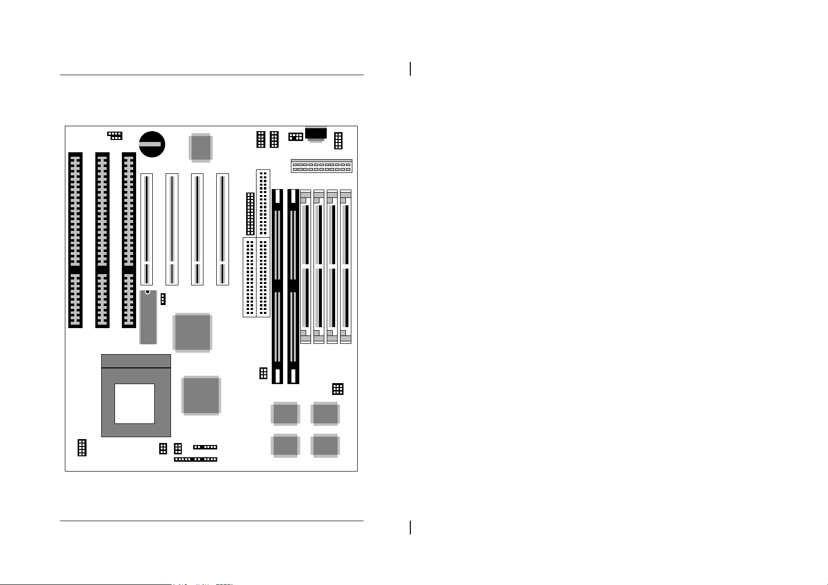
Mainboard Layout
Installation Procedures
1
IR1
JP1
SL3 SL2 SL1
A
B
C
D
E
JP8
1
UM8670F
PCI4 PCI3 PCI2 PCI1
JP2
1
3
BIOS
VIA
Socket 7
VIA
HD-LED
TB-LED
TB-SW
AB
AB
1
1
JP10
J6 J3
J5
11
JP11
Keylock
J8 J7 J4
1
Speaker
RST
COM1 COM2
FDC1
PRN1
IDE2 IDE1
5V
3.3V
AB
1
JP6
DIMM2 DIMM1
PS1
2
1
J2
USB1
12
J1
SIMM1SIMM2SIMM3SIMM4
CBA
1
3
JP3
VIAVIA
CacheCache
Figure 2-1 Mainboard Component Layout
9
Page 10

MS5120 Mainboard Manual
Jumper Settings
Jumpers
You can configure hardware options by setting jumpers on the
motherboard. See figure 2-1 for jumper location. Some jumpers on the
board have three metal pins with each pin representing a different function.
To set a jumper, a black, white, or red cap containing metal contacts is
placed over the jumper pin(s) according to the required configuration. A
jumper is ÒshortedÓ when a cap has been placed on one or two of its pins.
NOTE : Users are not encouraged to change the jumper settings that are
not listed in this manual. Changing the jumper settings
improperly may adversely affect system performance.
Pins 2 and 3 are shorted with a jumper cap
P3 P2 P1
Pins 1 and 2 are shorted with a jumper cap
P3 P2 P1
10
The jumper is open
The jumper is shorted (closed)
Page 11

Installation Procedures
J2 Ð Power Supply Connector
Pin Description Pin Description
1 Power Good 7 Ground
2 +5V DC 8 Ground
3 +12V DC 9 Ð5V DC
4 Ð12V DC 10 +5V DC
5 Ground 11 +5V DC
6 Ground 12 +5V DC
USB1 Ð Universal Serial BUS
Connector
Pin Description Pin Description
1 +5V DC 2 +5V DC
3 Data Ð 4 Data Ð
5 Data + 6 Data +
7 Ground 8 Ground
9 N.C. 10 N.C.
J3 Ð HDD LED Connector
Pin Description
+ +5V DC
Ð Active Low
Connectors:
COM1 Serial Port #1
COM2 Serial Port #2
PRN1 Parallel Port
IDE1 Primary IDE Port
IDE2 Secondary IDE Port
J1 Ð Keyboard Connector
Pin Description
1 Keyboard Clock
2 Keyboard Data
3 N.C.
4 Ground
5 +5V DC
J7 Ð System Reset
Setting Description
1 Ground
2 Reset System
JP2 Ð Flash ROM
Setting Description
P1, P2 12V Flash ROM
(default)
P2, P3 5V Flash ROM
JP6 Ð DIMM Module Voltage
Setting 5V 3.3V
A P1, P2 P2, P3
B P1, P2 P2, P3
11
Page 12

MS-5120 Mainboard Munual
J8 Ð Keylock & Power LED
Connector
Pin Description
1 LED Output
2 N.C.
3 Ground
4 Keylock
5 Ground
J4 Ð Speaker Connector
Pin Description
1 Data Out
2 N.C.
3 Ground
4 +5V
JP1 Ð Clear CMOS
Setting Description
Open Normal (default)
Close Clear CMOS
JP3A, B, C Ð CPU Speed Selectors
Settings 50MHz 55MHz 60MHz 66MHz 75MHz
A P2, P3 P1, P2 P2, P3 P2, P3 P1, P2
B P2, P3 P2, P3 P2, P3 P1, P2 P2, P3
C P2, P3 P2, P3 P1, P2 P2, P3 P1, P2
JP11A, B Ð CPU Internal Clock Speed Selectors
Settings 1.5X 2.0X 2.5X 3.0X
A P1, P2 P2, P3 P2, P3 P1, P2
B P1, P2 P1, P2 P2, P3 P2, P3
JP8 Ð CPU Voltage Selectors
Settings 3.5V 3.3V 3.2V 2.9V 2.8V
Position A B C D E
* All open is for 2.5V.
12
Page 13

JP10 Ð CPU Type Selectors
Settings P54C P55C
A P1, P2 P2, P3
B P1, P2 P2, P3
Installation Procedures
PS/2 Mouse Connector
Pin Description
1 Mouse CLK
2 Ground
3 N.C.
4 Mouse Data
5 N.C.
6 N.C.
7 N.C.
8 +5VDC
IR1 Ð Infra Red
Pin Description
1 IR In
2 Ground
3 IR Out
4 +5V DC
Memory Bank
Bank 0/1 Bank 2/3 Bank 4/5
DIMM2 SIMM 1, 2 SIMM 3,4
DIMM1
* SIMM 3,4 and DIMM1 can not be use at the same time. When using
SDRAM, JP6 must be set to 3.3V position and make sure the SDRAM
is with buffer.
13
Page 14

Chapter 3
HHHHoooowwww ttttoooo IIIIddddeeeennnnttttiiiiffffyyyy YYYYoooouuuurrrr BBBBIIIIOOOOSS
Boot-up your computer. Look at the top left corner for ÒRELEASE DATE
FOR THE BIOSÓ. You will find L or S at the end of the release date.
(Example: 04/28/1997L or 04/28/1997S)
SS
How to Update and Flash Your BIOS
Download the correct BIOS files from our website or BBS
¥ Uncompress files into a temporary directory ( you should end up with
two files)
¥ Boot the system without using any memory manages either from
bootable floppy disk or internal hard disk
¥ Run the flash utility (awflash.exe) and enter the full name of
XXXX.bin file
¥ Follow the screen instructions to update the BIOS (Do not turn off the
power during flash)
¥ After a successful flash, power down the system and clear the CMOS
with the appropriate jumper (Please refer to motherboard manual to
find the proper jumper). Short the jumper for 5-10 seconds then remove
the jumper and power the system on. This will clear any extraneous
data that may have been kept from the previous version of the BIOS.
14
Page 15

Award BIOS Setup
AAAAwwwwaaaarrrrdddd BBBBIIIIOOOOSSSS SSSSeeeettttuuuupp
The mainboard comes with the Award BIOS chip that contains the ROM
Setup information of your system. This chip serves as an interface between
the processor and the rest of the mainboardÕs components. This chapter
explains the information contained in the Setup program and tells you how
to modify the settings according to your system configuration.
pp
CMOS Setup Utility
A Setup program, built into the system BIOS, is stored in the CMOS RAM
that allows the configuration settings to be changed. This program is
executed when the user changes system configuration, the user changes
system backup battery, or the system detects a configuration error and asks
the user to run the Setup program.
Standard CMOS Setup
System BIOS automatically detects memory size, thus no changes are
necessary. However several items may require setting such as the system
Date and Time, IDE hard disk, floppy disk drive types for drive A: and B:,
boot up video display mode, or POST error handkling selection. Use the
arrow keys to highlight the item and then use the PgUp, or PgDn keys to
select the value you want in each item.
Hard Disk Configurations
TYPE
Select from 1 to 45 to fill remaining fields with predefined values of
disk drives. Select User to fill the remaining fields. Select Auto to
detect the HDD type automatically.
15
Page 16

MS5120 Mainboard Manual
SIZE
The hard disk size in Mega bytes.
CYLS
The cylinder number of the hard disk.
HEAD
The read/write head number of hard disk. The range is from 1 to 16.
PRECOMP
The cylinder number at which the disk drive changes the write timing.
LANDZ
The cylinder number that the disk drive heads (read/write) are seated
when the disk drive is parked.
SECTOR
The sector number of each track defined on the hard disk. The range is
from 1 to 64.
MODE
Select Auto to detect the mode type automatically. If your hard disk
supports the LBA mode, select LBA or Large. However, if your hard
disk cylinder is more than 1024 and does not support the LBA function,
then use the large setting. Select Normal if your hard disk supports
1024 cylinders or below 1024.
16
Page 17

Award BIOS Setup
BIOS Features Setup
Moving around the BIOS and Chipset Features Setup programs (refer to the
next section) works the same way as moving around the Standard CMOS
Setup program. Users are not encouraged to run the BIOS and Chipset
Features Setup programs. Your system should have been fine-tuned before
shipping. Improper Setup may cause the system to fail, so consult your
dealer before making any changes.
Virus Warning
When enabled, assigns the BIOS to monitor the master boot sector and
the DOS boot sector of the first hard disk drive for viruses.
The options are: Enabled, Disabled (Default).
CPU Internal Cache
When enabled, improves the system performance. Disable this item
when testing or trouble-shooting.
The options are: Enabled (Default), Disabled.
External Cache
When enabled, supports an optional cache SRAM.
The options are: Enabled (Default), Disabled.
Quick Power On Self Test
When enabled, allows the BIOS to bypass an extensive memory test.
The options are: Enabled, Disabled (Default).
17
Page 18

MS5120 Mainboard Manual
Boot Sequence
Allows the system BIOS to first try to boot the operating system from
the selected disk drive.
The options are: A, C (Default); C, A; C, CDROM, A; CDROM, C, A.
Swap Floppy Drive
When enabled, allows you to switch the order in which the operating
system accesses the floppy drives during boot up.
The options are: Enabled, Disabled (Default).
Boot Up Floppy Seek
When enabled, assigns the BIOS to perform floppy diskette drive tests
by issuing the time-consuming seek commands.
The options are: Enabled (Default), Disabled.
Boot Up Numlock Status
When set to On, allows the BIOS to automatically enable the Num
Lock Function when the system boots up.
The options are: On (Default), Off.
Boot Up System Speed
Allows to selection the boot up at high or low system speed.
Gate A20 Option
When Fast, allows the A20G bus line signal generated from the chipset
to directly pass to port 92H, instead of the keyboard controller. It will
speed up the system performance.
The options are: Fast (Default), Normal.
18
Page 19

Award BIOS Setup
Typematic Rate Setting
The term typematic means that when a keyboard key is held down, the
character is repeatedly entered until the key is released. When this item
is enabled, you may change the typematic repeat rate.
The options are: Disabled (Default), Enabled.
Typematic Rate (Chars/Sec)
Sets the rate of a character repeat when the key is held down.
The options are: 6 (Default), 8, 10, 12, 15, 20, 24, 30.
Typematic Delay (Msec)
Sets the delay time before a character is repeated.
The options are: 250 (Default), 500, 750, and 1000 millisecond.
Security Option
Allows you to set the security level of the system.
The options are: Setup (Default), System.
IDE Second Channel control
Allows you to enable or disable the IDE secondary channel
PS/2 mouse function control
Allows you to enable or disable PS/2 mouse function
Assign IRQ VGA
Choose enable or disable, to assign IRQ for VGA Card.
19
Page 20

MS5120 Mainboard Manual
Video BIOS Shadow
When enabled, allows the BIOS to copy the video ROM code of the
add-on video card to the system memory for faster access.
The options are: Enabled (Default), Disabled.
C8000-CBFFF to DC000-DFFFF Shadow
When enabled, allows the BIOS to copy the BIOS ROM code of the
add-on card to system memory for faster access. It may improve the
performance of the add-on card. Some add-on cards will not function
properly if its BIOS ROM code is shadowed. To use these options
correctly, you need to know the memory address range used by the
BIOS ROM of each add-on card.
The options are Enabled and Disabled (Default).
Chipset Features Setup
The Chipset Features Setup is used to control the values of the chipset
register. These registers control most of system options in the computer.
Auto configuration : Disable
Video BIOS Cacheable : Disable
System BIOS Cacheable : Disable
Cache Timing : Fast
DRAM Timing Control : Normal
Reduce DRAM Leadoff Cycle : Disable
The first six items are optimal setting for this motherboard, you should not
change them unless you are familiar with the Intel chipset.
20
Page 21

Award BIOS Setup
Power Management Setup
Power Management
When enabled, allows you to use Power Management features.
The options are: Enabled and Disabled (Default).
PM Control by APM
Option No allows the BIOS to ignore the APM (Advanced Power
Management) specification. Selecting Yes will allow the BIOS to wait
for APM's prompt before it enters Doze mode, Standby mode, or
Suspend mode. If the APM is installed, it will prompt the BIOS to set
the system into the power saving mode after all tasks are done.
The options are: Yes (Default) and No.
Video Off Option
This feature provides the selections of the video display power saving
mode. The option Suspend - Off allows the video display to go blank if
the system enters Suspend mode. The option All Modes - Off allows
the video display to go blank if the system enters Doze mode or
Suspend mode. The option Always On allows the video display to stay
in Standby mode even when the system enters Doze or Suspend mode.
The options are: Suspend - Off (Default), and all Modes - Off, Always
On.
Video Off Method
The option V/H SYNC+Blank allows the BIOS to blank off screen
display by turning off the V-Sync and H-Sync signals sent from the
add-on VGA card. DPMS Support allows the BIOS to blank off screen
display by your add-on VGA card, which supports DPMS (Display
Power Management Signaling function.) Blank Screen allows the
BIOS to blank screen display by turning off the red-green-blue signals.
21
Page 22

MS5120 Mainboard Manual
The options are: DPMS Support (Default), V/H SYNC+Blank, and
Blank Screen.
MODEM Use IRQ
This feature allows you to select the IRQ# to meet your modem's
IRQ#.
The options are: NA, 3 (Default), 4, 5,7, 9, 10 and 11.
HDD Power Management
Selecting Disabled will turn off the hard disk drive (HDD) motor.
Selecting 1 Min..15 Min allows you to define the HDD idle time before
the HDD enters Power Saving Mode. The option When Suspend lets
the BIOS turn the HDD motor off when the system is in Suspend
mode.
The options 1 Min..15 Min and When Suspend will not work
concurrently. When HDD is in Power Saving Mode, any access to the
HDD will wake the HDD up.
The options are: Disabled (Default), 1 Min..15 Min, and When
Suspend.
Doze Mode
When disabled, the system will not enter Doze mode. The specified
time option defines the idle time the system takes before it enters Doze
mode.
The options are: Disabled (Default), 10, 20, 30, 40 sec, 1, 2, 4, 6, 8, 10,
20, 30, 40 min, and 1 hour.
22
Page 23

Award BIOS Setup
Suspend Mode
When disabled, the system will not enter Suspend mode. The specified
time option defines the idle time the system takes before it enters
Suspend mode.
The options are: Disabled (Default), 10, 20, 30, 40 sec, 1, 2, 4, 6, 8, 10,
20, 30, 40 min, and 1 hour.
VGA
Selecting ON will enable the power management timers when a Òno
activity eventÓ is detected in the VGA. Selecting OFF will disable the
PM timer even if a no activity event is detected.
The options are: OFF (Default) and ON.
LPT & COM
Selecting LPT & COM will enable the power management timers when
a no activity event is detected in the LPT and COM ports. Selecting
LPT (COM) will enable the power management timers when a no
activity event is detected in the LPT (COM) ports. Selecting NONE
will disable the PM timer even if a no activity event is detected.
The options are: LPT & COM (Default), LPT, COM, and NONE.
HDD & FDD
Selecting ON will enable the power management timers when a no
activity event is detected in the hard disk drive and floppy disk drive.
Selecting OFF will disable the PM timer even if a no activity event is
detected.
The options are: OFF and ON (Default).
23
Page 24

MS5120 Mainboard Manual
IRQ# Activity
After the time period that you set in the Suspend Mode Feature, the
system advances from Doze Mode to Suspend Mode, in which the CPU
clock stops and the screen display is off. At this moment, if the IRQ
activity that is defined as Primary occurs, then the system goes back to
Full-on Mode directly.
If the IRQ activity that is defined as Secondary takes place, the system
enters another low power state, Dream Mode. The system will act as
Full-on Mode, except the screen display will remain off until the
corresponding IRQ handler finishes, then will revert back to Suspend
Mode.
For instance, if the system connects to a LAN and receives an
interruption from its file server, the system will enter the Dreaming
Mode to execute the corresponding calling routine.
The options are: Primary and Secondary.
The default values of IRQ3, 4, 5, 7, 9, 10, 11, 12, 14, 15 are: Primary.
The default value of IRQ8 is: Secondary.
PNP/PCI Configurations
Resources Controlled By
If you set at Auto, the BIOS automatically arranges all system
resources for you. If there are conflicts or you are not satisfied with the
configuration, simply set all the resources listed in the above figure by
selecting Manual.
The options are: Auto (default), Manual.
The manual options of IRQ/DMA assigned to are: Legacy ISA,
PCI/ISA PnP.
24
Page 25

Award BIOS Setup
Reset Configuration Data
When enabled, this feature allows the system to clear the last BIOS
configuration data and reset them with the default BIOS configuration
data.
The options are: Enabled and Disabled (default).
PCI IRQ Actived By
If your IDE card is triggered by Edge, set it at Edge.
The options are: Level (Default), Edge.
PCI IDE IRQ Map To
Set to Auto to allow the system BIOS to automatically detect which
interrupt is being used by the PCI master drive.
The options are: PCI-AUTO (Default), PCI-SLOT1, PCI-SLOT2, PCI-
SLOT3, PCI-SLOT4, and ISA.
Load Setup Defaults
Selecting this field loads the factory defaults for BIOS and Chipset values.
These settings are recommended for optimum performance. If the CMOS is
corrupted when entering the BIOS setup utility, you must reload setup
default.
Integrated Peripherals
IDE HDD Block Mode
When enabled, allows the system to execute read/write requests to hard
disk in block mode.
The options are: Enabled (Default), Disabled.
25
Page 26

MS5120 Mainboard Manual
IDE Primary Master PIO
Allows you to select first PCI IDE channel of the primary master hard
disk mode or to detect it by the BIOS.
The options are: Auto (Default), Mode 0, Mode 1, Mode 2, Mode 3,
Mode 4.
IDE Primary Slave PIO
Allows you to select the first PCI IDE channel of the primary slave
hard disk mode or to detect it by the BIOS.
The options are: Auto (Default), Mode 0, Mode 1, Mode 2, Mode 3,
Mode 4.
IDE Secondary Master PIO
Allows you to select first PCI IDE channel of the primary master hard
disk mode or to detect it by the BIOS.
The options are: Auto (Default), Mode 0, Mode 1, Mode 2, Mode 3,
Mode 4.
IDE Secondary Slave PIO
Allows you to select the first PCI IDE channel of the primary slave
hard disk mode or to detect it by the BIOS.
The options are: Auto (Default), Mode 0, Mode 1, Mode 2, Mode 3,
Mode 4.
On-chip Primary PCI IDE
When enabled, allows the IDE drive to use the first channel of the
primary IDE.
The options: Enabled (Default), Disabled.
26
Page 27

Award BIOS Setup
On-chip Secondary PCI IDE
When enabled, allows the IDE drive to use the second channel of the
primary IDE.
The options are: Enabled (Default), Disabled.
Onboard FDD Control
When enabled, the floppy diskette drive (FDD) controller is activated.
The options are: Enabled (Default), Disabled.
Onboard Serial Port 1
If the serial port 1 uses the onboard I/O controller, you can modify your
serial port parameters. If an I/O card needs to be installed, COM3 and
COM4 may be needed.
The options are: Auto, 3F8/IRQ4 (Default), 3E8/IRQ4, 2E8/IRQ3,
2F8/IRQ3, Disabled.
Onboard Serial Port 2
If the serial port 2 uses the onboard I/O controller, you can modify your
serial port parameters. If an I/O card needs to be installed, COM3 and
COM4 may be needed.
The options are :Auto, 2F8/IRQ3 (Default), 3E8/IRQ4, 2E8/IRQ3,
3F8/IRQ4, Disabled.
Onboard Parallel Port
Allows you to select from a given set of parameters if the parallel port
uses the onboard I/O controller.
The options are: 378H/IRQ7 (Default), 278H/IRQ5, 3BCH/IRQ7,
Disabled.
27
Page 28

MS5120 Mainboard Manual
Onboard Parallel Mode
Allows you to connect with an advanced printer I/O mode.
The options are: SPP (Default), EPP, ECP, ECP/EPP.
ECP Mode Use DMA 3
Allows you to select DMA channel 3 or 1 for the ECP printer mode.
Parallel Port EPP Type
Allows you to select the EPP parallel port.
Supervisor/User Password
To enable the Supervisor/User passwords, select the item from the Standard
CMOS Setup. You will be prompted to create your own password. Type
your password (up to eight characters) and press <Enter>. You will be
asked to confirm the password. Type the password again and press<Enter>.
You may also press <Esc> to abort the selection and not enter a password.
To disable password, press <Enter> when you are prompted to enter
password. A message appears, confirming the password is disabled.
Under the BIOS Feature Setup, if System is selected under the Security
Option field and the Supervisor Password is enabled, you will be prompted
for the Supervisor Password every time you try to enter the CMOS Setup
Utility. If System is selected and the User Password is enabled, you will be
asked to enter the User Password every time you reboot the system. If
Setup is selected under the Security Option field and the User Password is
enabled, you will be prompted only when you reboot the system.
28
Page 29

Award BIOS Setup
IDE HDD Auto Detection
The IDE Hard Disk Drive Auto Detection feature automatically configures
your new hard disk. Use it for a quick configuration of new hard disk
drives. This feature allows you to set the parameters for up to four IDE
HDDs. The option with (Y) is recommended by the system BIOS. You
may also key in your own parameters instead of using the preset setting by
the system BIOS. After configuring all of the settings, press <Esc> key to
return the main menu. For confirmation, enter the Standard CMOS Setup
feature.
Save and Exit Setup
After you have made changes under Setup, press <Esc> to return to the
main menu. Move cursor to ÒSave and Exit SetupÓ or press <F10> and then
press <Y> to change the CMOS Setup. If you did not change anything,
press <Esc> again or move cursor to ÒExit Without SavingÓ and press <Y>
to retain the Setup settings. The following message will appear at the center
of the screen to allow you to save data to CMOS and exit the setup utility:
SAVE to CMOS and EXIT (Y/N)?
Exit without Saving
If you select this feature, the following message will appear at the center of
the screen to allow you to exit the setup utility without saving CMOS
modifications: Quit Without Saving (Y/N)?
Note: Default values of the various Setup items in this chapter may not be
the same ones shown on your screen.
29
Page 30

Appendix
CCCCPPPPUUUU TTTTaaaabbbbllllee
CPU CPU BUS Clock Multiplier
75MHz 50MHz 1.5
90MHz 60MHz 1.5
100MHz 66MHz 1.5
120MHz 60MHz 2.0
Intel 133MHz 66MHz 2.0
150MHz 60MHz 2.5
166MHz 66MHz 2.5
200MHz(MMX) 66MHz 3.0
233MHz(MMX) 66MHz 1.5
PR75 50MHz 1.5
PR90 60MHz 1.5
PR100 66MHz 1.5
PR133 66MHz 1.5
AMD K5-166 66MHz 2.5
K6-166 66MHz 2.5
K6-200 66MHz 3.0
K6233 66MHz 1.5
Cyrix
+
P120
+
P133
+
P150
+
P166
MX-166 60MHz 2.5
MX-200 66MHz 2.5
50MHz 2.0
55MHz 2.0
60MHz 2.0
66MHz 2.0
ee
30
Page 31

Award BIOS Setup
31
 Loading...