

1A, PWM Step-Down DC/DC Converter
MT5201
DESCRIPTION
The MT5201 is a step-down, current mode, DC-DC converter. At heavy load, the constant-frequency PWM control
performs excellent stability and transient response. To ensure the longest battery life in portable applications, the
MT5201 have a power-saving Pulse-skipping Modulation (PSM) mode and reduce the quiescent current under light
load operation to save power.
The MT5201 is supported with a range of input voltages form 2.5V to 5.5V allowing the use of a single
Li+/Li-polymer cell, multiple Alkaline/NiMH cell, USB, and other standard power sources. The output voltage is
adjustable from 0.6V to the input voltage, while the suffix part numbers MT5201-X.X indicate pre-set voltage ranges of
3.3V, 1.8V, 1.5V or 1.2V. All versions Include internal power switch and synchronous rectifier for minimal external part
count and high efficiency. During the shutdown, the input is disconnected form the output and the shutdown current is
less than 0.1uA. Other key features include under-voltage lockout to prevent deep-battery discharge.
FEATURES
¾ Efficiency up to 96%
APPLICATIONS
¾ Cellular phone
¾ Only 40uA(TYP.) Quiescent Current
¾ Up to 1A
¾ Internal Synchronous Rectifier
¾ 1.5MHz Switching Frequency
¾ Under-Voltage Lockout
¾ Short Circuit Protection
¾ 5-pin Small SOT-23-5 Package
¾ Pb-Free Package
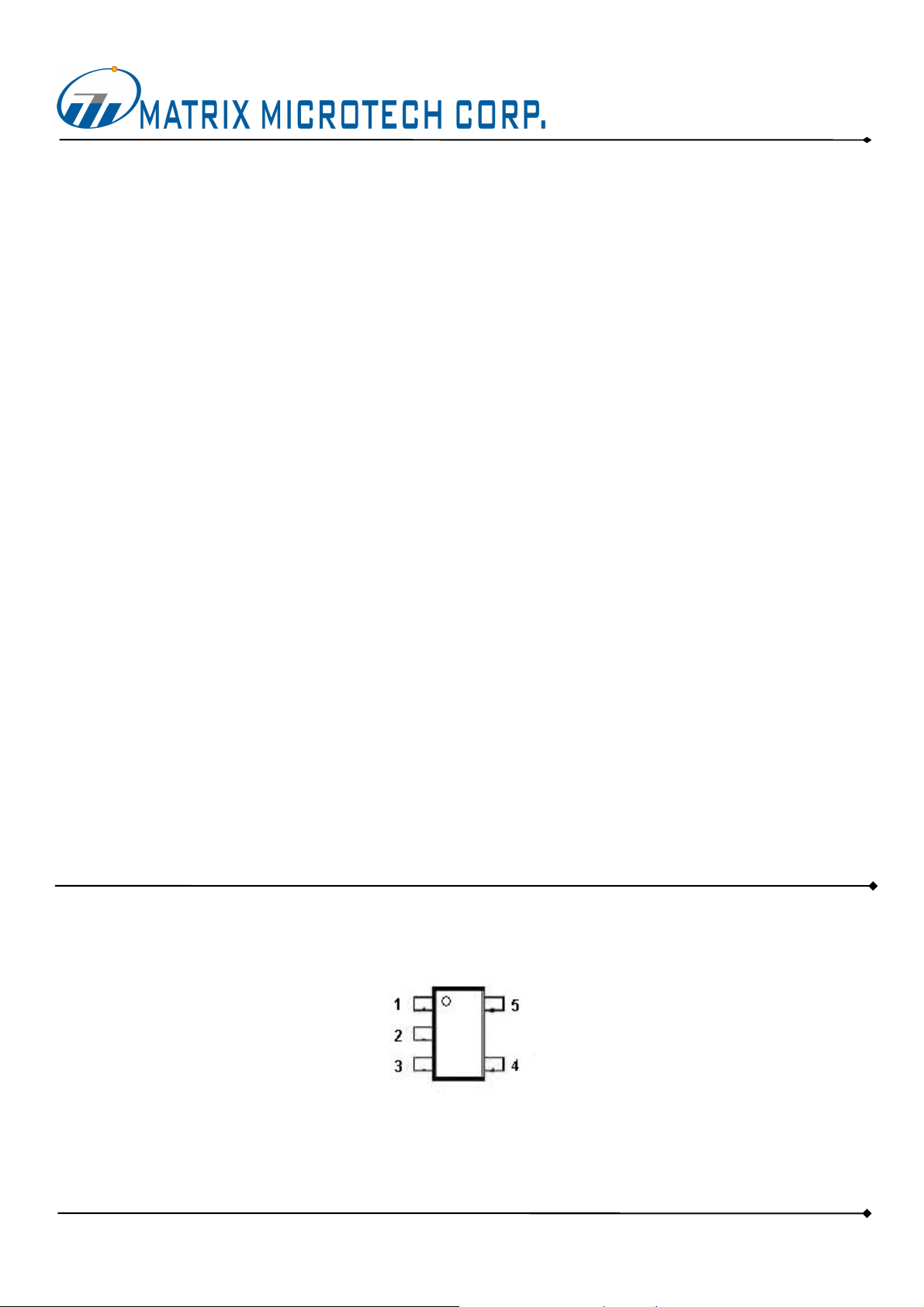
PIN CONFIGURATIONS
SOT-23-5 (Top View)
¾ Portable electronics
¾ Wireless Devices
¾ Cordless phone
¾ Computer peripherals
¾ Battery Powered Widgets
¾ Electronic scales
MT5201-X.XN
- 1 - www.matrix-microtech.com.tw.
1A, PWM Step-Down DC/DC Converter
PIN CONFIGURATION
Pin Number Name Function
1 EN Enable(active high)
2 GND Ground
3 SW Switch
4 VIN Input
5 VOUT/FB Output/Feedback
ORDERING INFORMATION
MT5201
Device Package
V
Volts
OUT
TA (OC)
MT5201-X.XN N SOT-23-5L X.X_ 3.3/ 1.8/ 1.5/ 1.2/ ADJ 0-85
POWER DISSIPATION TABLE
θ
Package
JA
(OC /W )
Power rating(mW)
N 250 400 220 160
≤ 25 OC
T
A
TA=70 OC
Power rating(mW)
TA= 85 OC
Power rating (mW)
Note :
1. Exceeding the maximum allowable power dissipation will result in excessive die temperature, and the regulator will go into
thermal shutdown.
J: Junction Temperature Calculation:
2. T
= TA + (PD × θJA)
T
J
numbers are guidelines for the thermal performance of the device/PC-board system. All of the above assume no
The θ
JA
ambient airflow.
3. θ
Thermal Resistance-Junction to Ambient.
JA:
ABSOLUTE MAXIMUM RATINGS
Symbol Parameter Maximum Unit
Input Voltage VIN 6.6 V
EN, FB Pin Voltage VEN
SW Pin Voltage V
SW
-0.3 to V
-0.3 to (VIN +0.3) V
V
IN
Junction Temperature TJ 125 OC
Storage Temperature Range T
Soldering Temperature Range T
Note :
These are stress ratings only and functional operation is not implied. Exposure to absolute maximum ratings for prolonged time
periods may affect device reliability. All voltages are with respect to ground.
- 65 to 150
STG
300/5sec OC
OPR
O
C
- 2 - www.matrix-microtech.com.tw.
RECOMMENDED OPERATING CONDITIONS
MT5201
1A, PWM Step-Down DC/DC Converter
Parameter
Supply Voltage
Supply Voltage( for Max.duration of 30 Min.)
Operating Temperature
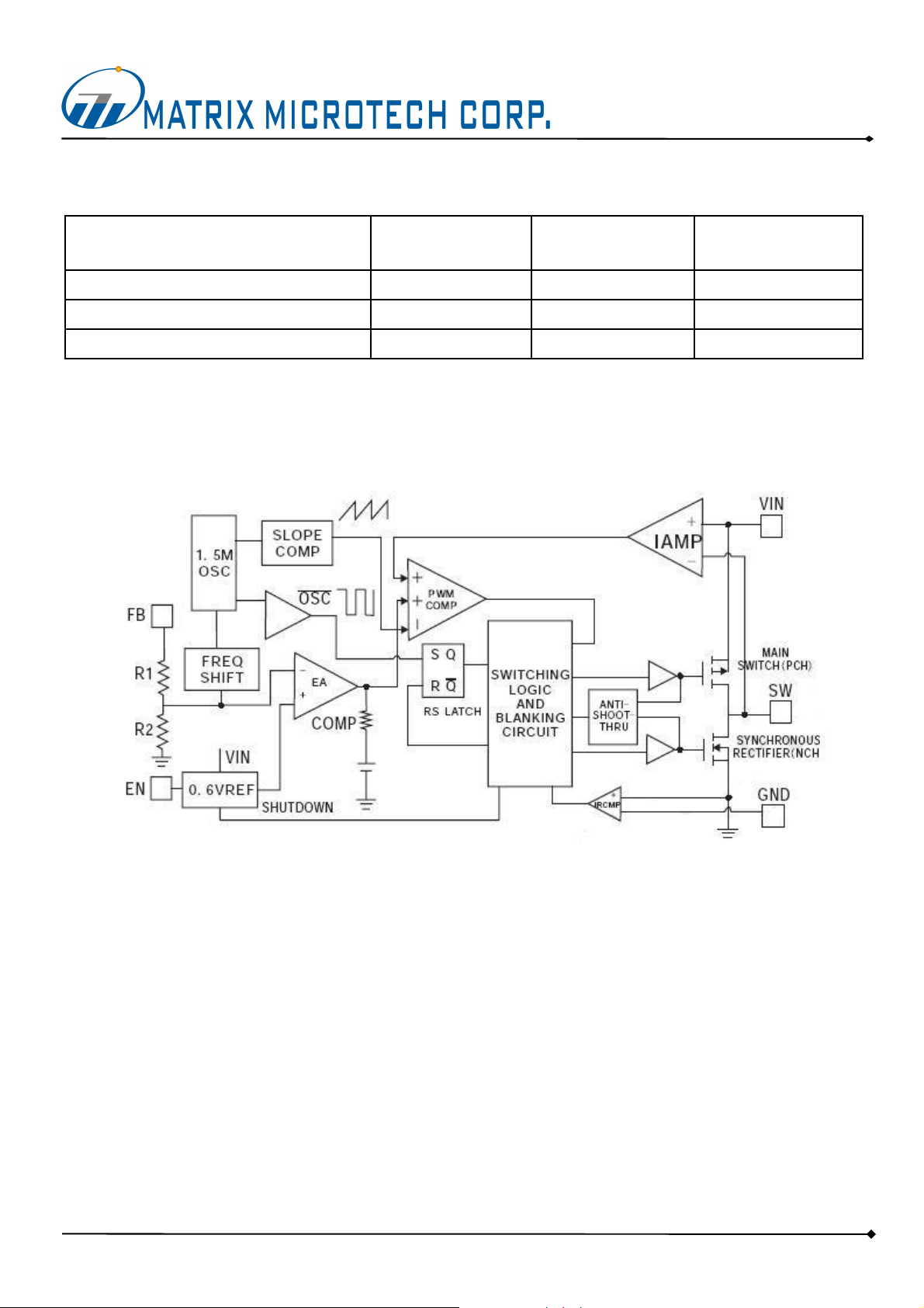
BLOCK DIAGRAM
Symbol Max Unit
5.5
6.0
85
V
V
O
C
T
V
V
CC
CC
OPR
- 3 - www.matrix-microtech.com.tw.

ELECTRICAL CHARACTERISTICS
TA=25℃, VIN=5V, VO=1.8V, CIN=10uF, CO=10uF, L=4.7uH, unless otherwise noted.
MT5201
1A, PWM Step-Down DC/DC Converter
Parameter Symbol Conditions Min. Typ. Max.
Input Voltage Range VIN 2.5 - 5.5 V
Regulated Feedback Voltage VFB 0.588 0.6 0.612 V
Reference Voltage Line Regulation VFB - 0.3 - %/V
Regulated Output Voltage Accuary VO I
Peak Inductor Current IPK V
Output Voltage Line Regulation LNR VIN=2.5V to 5.5V,IO=10mA - 0.2 - %/V
Output Voltage Load Regulation LDR IO=1mA to 1A - 0.5 - %
Quiescent Current IQ No load - 40 70 uA
Shutdown Current ISD VEN=0V - 0.01 1 uA
Oscillator Frequency F
Drain-Source On-State Resistance R
SW Leakage Current I
OSC
DS(ON)
- ±0.01 1 uA
LSW
=100mA -3 - +3 %
O
=3V, VFB=0.5V or VO=90% - 1.4 - A
IN
VO=100% 1.2 1.5 1.8 Mhz
V
=0V or VO=0V - 500 - KHz
FB
IDS=100mA
P MOSFET - 0.45 - Ω
N MOSFET - 0.4 - Ω
Uni
t
High Efficiency η - 96 - %
EN Threshold High VEH 1.3 - - V
EN Threshold Low VEL - - 0.4 V
EN Leakage Current IEN - ±0.01 - uA
TYPICAL APPLICATIONS
- 4 - www.matrix-microtech.com.tw.

MT5201
1A, PWM Step-Down DC/DC Converter
APPLICATION INFORMATION
The basic MT5201 application circuit is shown in Page4. External component selection is driven by the load
requirement and begins with the selection of L followed by C
and C
IN
OUT.
Inductor Selection
For most applications, the value of the inductor will fall in the range of 1µH to 4.7µH. Its value is chosen based on the
desired ripple current. Large value inductors lower ripple current and small value inductors result in higher ripple
currents. Higher V
setting ripple current is ΔI
or V
IN
also increases the ripple current as shown in equation1. A reasonable starting point for
OUT
=240mA(40% of 600mA).
L
……..(1)
The DC current rating of the inductor should be at least equal to the maximum load current plus half the ripple current
to prevent core saturation. Thus, a 720mA rated inductor should be enough for most applications (600mA+120mA).
For better efficiency, choose a low DC-resistance inductor.
C
IN
and C
Selection
OUT
In continuous mode, the source current of the top MOSFET is a square wave of duty cycle V
OUT/VIN
. To prevent large
voltage transients, a low ESR input capacitor sized for the maximum RMS current must be used. The maximum RMS
capacitor current is given by:
This formula has a maximum at VIN=2Vout, where I
=Iout/2. This simple worst-case condition is commonly used for
RMS
design because even significant deviations do not offer much relief. Note that the capacitor manufacturer's ripple
current ratings are often based on 2000 hours of life. This makes it advisable to further derate the capacitor, or choose
a capacitor rated at a higher temperature than required. Consult the manufacturer if there is any question.
The selection of C
is driven by the required effective series resistance (ESR)
OUT
- 5 - www.matrix-microtech.com.tw.

APPLICATION INFORMATION (Cont.)
MT5201
1A, PWM Step-Down DC/DC Converter
Typically, once the ESR requirement for C
(P-P) requirement. The output ripple △V
Where f=operating frequency, C
voltage, the output ripple is highest at maximum input voltage since ΔI
Using Ceramic Input ad Output Capacitors
Higher values, lower cost ceramic capacitors are now becoming available in smaller case sizes. Their high ripple
current, high voltage rating and low ESR make them ideal for switching regulator applications. Using ceramic
capacitors can achieve very low output ripple and small circuit size.
When choosing the input and output ceramic capacitors, choose the X5R or X7R dielectric formulations. These
dielectrics have the best temperature and voltage characteristics of all the ceramics for a given value and size.
=output capacitance and ΔIL= ripple current in the inductor. For a fixed output
OUT
has been met, the RMS current rating generally far exceeds the I
OUT
is determined by:
OUT
increases with input voltage.
L
RIPRLE
- 6 - www.matrix-microtech.com.tw.

TYPICAL PERFORMANCE CHARACTERISTICS
MT5201
1A, PWM Step-Down DC/DC Converter
- 7 - www.matrix-microtech.com.tw.

TYPICAL PERFORMANCE CHARACTERISTICS
MT5201
1A, PWM Step-Down DC/DC Converter
- 8 - www.matrix-microtech.com.tw.

PHYSICAL DIMENSIONS:
SOT-23-5L
MT5201
1A, PWM Step-Down DC/DC Converter
- 9 - www.matrix-microtech.com.tw.

 Loading...