


PXA300 and PXA310 Processor
Vol. I: System and Timer Configuration
Developers Manual, Rev 0.94
Product Number to be assigned at a later date.
Doc. No. MV-TBD-00, Rev. A
MARVELL CONFIDENTIAL, UNDER NDA# 12101050
69rlq62d-f714peg4 * Memec (Headquarters) - Unique Tech, Insight, Impact
December 13, 2006
Document Classification: Proprietary Information
Not approved by Document Control. For review only.
MARVELL CONFIDENTIAL - UNAUTHORIZED DISTRIBUTION OR USE STRICTLY PROHIBITED
MARVELL CONFIDENTIAL, UNDER NDA# 12101050
69rlq62d-f714peg4 * Memec (Headquarters) - Unique Tech, Insight, Impact * UNDER NDA# 12101050
69rlq62d-f714peg4 * Memec (Headquarters) - Unique Tech, Insight, Impact
Product Number
Developers Manual
Document Conventions
Note
Provides related information or information of special importance.
Caution
Indicates potential damage to hardware or software, or loss of data.
Warning
Indicates a risk of personal injury.
Document Status
Doc Status: Preliminary Technical Publication: 0.xx
MARVELL CONFIDENTIAL, UNDER NDA# 12101050
For more information, visit our website at: www.marvell.com
Disclaimer
69rlq62d-f714peg4 * Memec (Headquarters) - Unique Tech, Insight, Impact
No part of this document may be reproduced or transmitted in any form or by any means, electronic or mechanical, including photocopying and recording, for any
purpose, without the express written permission of Marvell. Marvell retains the right to make changes to this document at any time, without notice. Marvell makes no
warranty of any kind, expressed or implied, with regard to any information contained in this document, including, but not limited to, the implied warranties of
merchantability or fitness for any particular purpose. Further, Marvell does not warrant the accuracy or completeness of the information, text, graphics, or other items
contained within this document.
Marvell products are not designed for use in life-support equipment or applications that would cause a life-threatening situation if any such products failed. Do not use
Marvell products in these types of equipment or applications.
With respect to the products described herein, the user or recipient, in the absence of appropriate U.S. government authorization, agrees:
1) Not to re-export or rel ease any su ch info rma tion co nsi sting o f technology, software or source code controlled for national security reasons by the U.S. E xport Contr ol
Regulations ("EAR"), to a national of EAR Country Groups D:1 or E:2;
2) Not to export the direct product of such technology or such software, to EAR Country Groups D:1 or E:2, if such technology or software and direct products thereof
are controlled for national security reasons by the EAR; and,
3) In the case of technology controlled for national security reasons under the EAR where the direct product of the technology is a complete plant or component of a
plant, not to export to EAR Co untr y Gr oup s D:1 o r E :2 the dir ect p rodu ct o f th e p lant or maj or component thereof, if such d irect prod uct is controlled for nati onal security
reasons by the EAR, or is subject to controls under the U.S. Munitions List ("USML").
At all times hereunder, the recipient of any such infor matio n agr ees that they shall be deemed to have man ually sign ed th is docum ent in con necti on with their receipt of
any such information.
Copyright © 2006. Marvell International Ltd. All rights reserved. Marvell, the Marvell logo, Moving Forward Faster, Alaska, Fastwriter, Datacom Systems on Silicon,
Libertas, Link S treet, NetGX , PHYAdvantage, Prestera, Raising The Technology Bar, The T echnology Wi thin, V irtual C able Tester, and Yukon are re gistered tra demarks
of Marvell. Ants, AnyVoltage, Discovery, DSP Switcher, F eroce on, Ga lNet, Gal Tis, Horizon, Marvell Makes It A ll P ossible, RA DLA N, UniMAC , and VCT ar e tra dema rks
of Marvell. All other trademarks are the property of their respective owners.
Intel XScale® is a trademark or registered trademark of Intel Corporation and its subsidiaries in the United States and other countries.
MARVELL CONFIDENTIAL - UNAUTHORIZED DISTRIBUTION OR USE STRICTLY PROHIBITED
MARVELL CONFIDENTIAL, UNDER NDA# 12101050
Doc. No. MV-TBD-00 Rev. A
Page 2 Document Classification: Proprietary Information December 13, 2006
69rlq62d-f714peg4 * Memec (Headquarters) - Unique Tech, Insight, Impact
Not approved by Document Control. For review only.
CONFIDENTIAL
Copyright © 12/13/06 Marvell
69rlq62d-f714peg4 * Memec (Headquarters) - Unique Tech, Insight, Impact * UNDER NDA# 12101050

Contents
1 Introduction..................................................................................................................................19
1.1 About This Manual......... ....... ...... ....... ...... ....... ...... ...... ....... ...... ...........................................19
1.1.1 Number Representation.........................................................................................20
1.1.2 Naming Conventions .............................................................................................20
1.1.3 Data Types ............................................................................................................20
1.1.4 Related Documents ...............................................................................................21
1.2 Product Overview ...............................................................................................................22
1.2.1 Intel XScale
1.2.2 Intel XScale
1.2.3 Multimedia Coprocessor ....... ...... ....... ...... ............................................. ....... ...... ....24
1.2.4 Power Management...............................................................................................24
1.2.5 Power I2C Controller .............................................................................................25
1.2.6 One-Wire Controller...............................................................................................25
1.2.7 Graphics Controller................................................................................................26
1.2.8 Performance Monitor .............................................................................................27
1.2.9 Internal Memory Architecture.................................................................................27
1.2.10 Internal SRAM Memory .........................................................................................27
1.2.11 External Memory Interfaces...................................................................................27
1.2.12 Dynamic Memory Controller ..................................................................................28
1.2.13 Static Memory Controller .......................................................................................28
1.2.14 Data Flash Controller.............................................................................................29
1.2.15 Interrupt Controller.................................................................................................30
1.2.16 Operating System Timers......................................................................................30
1.2.17 Pulse-Width Modulation Unit (PWM) .....................................................................31
1.2.18 Real-Time Clock (RTC)..........................................................................................31
MARVELL CONFIDENTIAL, UNDER NDA# 12101050
1.2.19 General-Purpose I/O (GPIO) .................................................................................32
1.2.20 DMA Controller ......................................................................................................32
1.2.21 Mobile Scalable Link Controller .............................................................................33
1.2.22 Serial Ports ............................................................................................................33
69rlq62d-f714peg4 * Memec (Headquarters) - Unique Tech, Insight, Impact
1.2.23 LCD Panel Controller............................................ ...... ....... ...... ....... ...... ....... ..........37
1.2.24 Mini-LCD Panel Controller .....................................................................................38
1.2.25 Multimedia Card, SD Memory Card, and SDIO Card ............................................39
1.2.26 Keypad Interface....................................................................................................39
1.2.27 Universal Subscriber ID Controller.........................................................................40
1.2.28 Camera Image Capture Interface ..........................................................................40
1.2.29 Test........................................................................................................................42
1.3 Intel XScale
®
Microarchitecture Compatib ility ....................................................................42
®
Microarchitecture and Core.............................................................23
®
Microarchitecture Features............. ...... ....... ...... ..............................2 3
MARVELL CONFIDENTIAL - UNAUTHORIZED DISTRIBUTION OR USE STRICTLY PROHIBITED
2 System Architecture Overview...................................................................................................43
2.0.1 Differences Between PXA300 Processor and PXA310 Processor........................43
2.1 Intel XScale
2.2 Endianness.........................................................................................................................44
2.3 Memory Switch vs. System Bus .........................................................................................44
2.4 I/O Ordering........................................................................................................................44
2.5 Accessing Peripherals on Internal Per i phe ral Bus................... ....... ....................................45
2.5.1 Programmed I/O Operations Using the Bridge ......................................................45
Copyright © 12/13/06 Marvell
December 13, 2006 Document Classification: Proprietary Information Page 3
®
Microarchitecture Implementation Options...................................................43
MARVELL CONFIDENTIAL, UNDER NDA# 12101050
CONFIDENTIAL
69rlq62d-f714peg4 * Memec (Headquarters) - Unique Tech, Insight, Impact
Not approved by Document Control. For review only.
Doc. No. MV-TBD-00 Rev. A
69rlq62d-f714peg4 * Memec (Headquarters) - Unique Tech, Insight, Impact * UNDER NDA# 12101050

Product Number
Developers Manual
2.5.2 Data Transfer Using DMA......................................................................................45
2.6 Peripheral Access on Internal System Buses.....................................................................46
2.7 DMA/Peripheral Split Transactions.....................................................................................46
2.8 System Bus Arbiters ...........................................................................................................46
2.9 System Access Latencies...................................................................................................46
2.10 Semaphores .......................................................................................................................47
2.11 Interrupts.............................................................................................................................48
2.12 Reset ..................................................................................................................................48
2.13 Selecting Peripherals vs. General-Purpose I/O..................................................................49
2.14 Power-On Reset and Boot Operation.................................................................................49
2.15 Memory Map and Register Overview .................................................................................50
2.15.1 Intel XScale
2.15.2 Interrupt Controller Registers.................................................................................53
2.15.3 Performance Monitoring Registers........................................................................54
2.15.4 Clock Configuration and Power Management Registers.......................................55
2.15.5 Coprocessor Software Debug Registers ...............................................................55
2.15.6 Coprocessor 15 .....................................................................................................56
3 Memory Switch ............................................................................................................................61
3.1 Overview.............................................................................................................................61
3.1.1 Differences Between PXA300 Processor and PXA310 Processor........................61
3.2 Features..............................................................................................................................61
3.3 I/O Pins...............................................................................................................................62
3.4 Functional Description ............................................................................. ....... ...... ..............62
3.4.1 Priority Control.......................................................................................................62
3.4.2 The Memory Switch Concept.................................................................................64
®
Microarchitecture Coprocessor Register Summary.........................51
4 Pin Descriptions and Control.....................................................................................................65
69rlq62d-f714peg4 * Memec (Headquarters) - Unique Tech, Insight, Impact
MARVELL CONFIDENTIAL - UNAUTHORIZED DISTRIBUTION OR USE STRICTLY PROHIBITED
4.1 Overview.............................................................................................................................65
MARVELL CONFIDENTIAL, UNDER NDA# 12101050
4.1.1 Differences Between PXA300 and PXA310 Processors.......................................65
4.2 Features..............................................................................................................................65
4.3 PXA300 Processors Pin List with Alternate Functions .......................................................66
4.4 PXA310 Processor Pin List with Alternate Functions .........................................................75
4.5 Signal Descriptions.............................................................................................................86
4.6 Pin Control Unit Overview...................................................................................................99
4.6.1 Checking for Completion of a Multi-Function Pin Operation................................100
4.6.2 Access to Nonexistent Registers or Pins.............................................................100
4.6.3 Pin Control Unit Address Map .............................................................................100
4.7 Register Descriptions........................................................................................................110
4.8 Multi-Function Pin Block Diagram.....................................................................................113
4.8.1 Example...............................................................................................................113
4.9 Edge-Detect Operation.....................................................................................................116
4.10 Low-Power Mode Operation.............................................................................................116
4.11 Wakeup Detection ............................................................................................................118
4.11.1 Services Wakeups................................ ............................................. ...... ....... .....118
4.11.2 Peripheral Controller Wakeups............................................................................118
4.11.3 Generic Wakeups ................................................................................................119
4.11.4 Wake-up Functionality on Multi-Function Pins.....................................................120
MARVELL CONFIDENTIAL, UNDER NDA# 12101050
Copyright © 12/13/06 Marvell
December 13, 2006 Document Classification: Proprietary Information Page 4
69rlq62d-f714peg4 * Memec (Headquarters) - Unique Tech, Insight, Impact
Not approved by Document Control. For review only.
CONFIDENTIAL
Doc. No. MV-TBD-00 Rev. A
69rlq62d-f714peg4 * Memec (Headquarters) - Unique Tech, Insight, Impact * UNDER NDA# 12101050

5 General-Purpose I/O Unit..........................................................................................................123
5.1 Overview...........................................................................................................................123
5.2 Features............................................................................................................................124
5.3 Register Descriptions........................................................................................................125
5.3.1 GPIO Pin-Level Registers (GPLRx).....................................................................126
5.3.2 GPIO Pin Direction Registers (GPDRx)...............................................................127
5.3.3 GPIO Pin Bit-Wise Set Direction Registers (GSDRx)..........................................128
5.3.4 GPIO Pin Bit-Wise Clear Direction Registers (GCDRx).......................................129
5.3.5 GPIO Pin Output Set Registers (GPSRx) and Pin Output Clear Registers
(GPCRx) ..............................................................................................................130
5.3.6 GPIO Rising-Edge Detect-Enable Registers (GRERx)........................................131
5.3.7 GPIO Bit-Wise Set Rising-Edge (GSRERx) and GPIO Bit-wise Clear Rising-
Edge (GCRERx) Detect-Enable Registers ..........................................................132
5.3.8 GPIO Falling-Edge Detect-Enable Registers (GFERx)........................................134
5.3.9 GPIO Bit-Wise Set Falling-Edge (GSFERx) and GPIO Bit-wise Clear Falling-
Edge (GCFERx) Detect-Enable Registers...........................................................134
5.3.10 GPIO Edge Detect Status Register (GEDRx)......................................................136
5.4 Register Summary............................................................................................................137
6 Services Clock Control Unit .....................................................................................................141
6.1 Overview...........................................................................................................................141
6.1.1 Differences between the PXA300 Processor and PXA310 Processor ................142
6.2 Features............................................................................................................................142
6.3 Signal Descriptions...........................................................................................................142
6.3.1 Processor Oscillator In (PXTAL_IN) and Processor Oscillator Out
(PXTAL_OUT) .....................................................................................................143
6.3.2 Timekeeping Oscillator Input (TXTAL_IN) and Timekeeping Oscillator Output ........
(TXTAL_OUT)......................................................................................................143
6.3.3 Processor Clock Output (CLK_POUT).................................................................143
MARVELL CONFIDENTIAL, UNDER NDA# 12101050
6.3.4 Timekeeping Clock Output (CLK_TOUT) ............................................................144
6.3.5 VCTCXO Enable (VCTCXO_EN) ........................................................................144
6.4 Operation..........................................................................................................................144
6.4.1 System Clock Requirements................................................................................144
69rlq62d-f714peg4 * Memec (Headquarters) - Unique Tech, Insight, Impact
6.4.2 Functional Description .........................................................................................144
6.4.3 Processor Oscillator (13 MHz).............................................................................145
6.4.4 Timekeeping Oscillator (32.768 kHz)...................................................................146
6.4.5 Core Phase-Locked Loop (104–806 MHz) ..........................................................146
6.4.6 System Phase-Locked Loop (624 MHz)..............................................................146
6.4.7 Ring Oscillator (120 MHz ± 15%, 40 MHz ± 5%).................................................147
6.5 Register Descriptions........................................................................................................147
6.5.1 Oscillator Configuration Register (OSCC) ...........................................................147
6.6 Register Summary............................................................................................................149
MARVELL CONFIDENTIAL - UNAUTHORIZED DISTRIBUTION OR USE STRICTLY PROHIBITED
7 Slave Clock Control Unit...........................................................................................................151
7.1 Overview...........................................................................................................................151
7.2 Features............................................................................................................................151
7.2.1 Functional Description .........................................................................................151
7.2.2 Core Phase-Locked Loop (104–624 MHz) ..........................................................152
7.2.3 System Phase-Locked Loop (624 MHz)..............................................................156
MARVELL CONFIDENTIAL, UNDER NDA# 12101050
Copyright © 12/13/06 Marvell
December 13, 2006 Document Classification: Proprietary Information Page 5
69rlq62d-f714peg4 * Memec (Headquarters) - Unique Tech, Insight, Impact
Not approved by Document Control. For review only.
CONFIDENTIAL
Doc. No. MV-TBD-00 Rev. A
69rlq62d-f714peg4 * Memec (Headquarters) - Unique Tech, Insight, Impact * UNDER NDA# 12101050

8 Services Power Management Unit...........................................................................................179
69rlq62d-f714peg4 * Memec (Headquarters) - Unique Tech, Insight, Impact
MARVELL CONFIDENTIAL - UNAUTHORIZED DISTRIBUTION OR USE STRICTLY PROHIBITED
Product Number
Developers Manual
7.2.4 Ring Oscillator (120 MHz ± 15%) .......................................................................156
7.2.5 Ring Oscillator (40 MHz ± 5%) During D1 Mode .................................................160
7.2.6 Functional Clock Gating .... ....... ...... ....... ...... ...... ....... ...... ......................................160
7.2.7 Performing Peripheral Frequency Changes ........................................................161
7.2.8 Changing PLL State.............................................................................................161
7.2.9 Core Idle Mode ....................................................................................................161
7.2.10 Core Idle Mode Coupled with Software-Controlled Voltage Changes.................162
7.3 Register Descriptions........................................................................................................162
7.3.1 Application Subsystem Clock Configuration Register (ACCR)............................163
7.3.2 Application Subsystem Clock Status Register (ACSR) .......................................169
7.3.3 Application Subsystem Interrupt Control/Status Register (AICSR) .....................172
7.3.4 D0 Mode Clock Enable Register A (D0CKEN_A)................................................173
7.3.5 D0 Mode Clock Enable Register B (D0CKEN_B)................................................174
7.3.6 AC ’97 Clock Divisor Value Register (AC97_DIV)...............................................176
7.3.7 Coprocessor 14: Clock ........................................................................................177
7.4 Register Summary............................................................................................................178
8.1 Overview...........................................................................................................................179
8.2 Differences Between the PXA300 Processor and PXA310 Processor.............................180
8.3 Features............................................................................................................................180
8.4 Signal Descriptions...........................................................................................................181
8.4.1 Hardware Reset (nRESET) .................................................................................182
8.4.2 Reset Out (nRESET_OUT)..................................................................................182
8.4.3 GPIO Reset (nGPIO_RESET)........................................................... ...... ....... .....182
8.4.4 EXT_WAKEUP<1:0>...........................................................................................183
8.4.5 Battery Fault (nBATT_FAULT) ............................................................................183
8.4.6 System Power Enable (SYS_EN)........................................................................184
8.4.7 Power Enable (PWR_EN)....................................................................................184
MARVELL CONFIDENTIAL, UNDER NDA# 12101050
8.4.8 Power Management Unit I2C Clock (PWR_SCL)................................................184
8.4.9 Power Management Unit I2C Data (PWR_SDA)............................................ .....184
8.4.10 Power Management Unit Capacitor Pins (PWR_CAP<1:0>) ..............................184
8.4.11 Power Management Supply Output (PWR_OUT) ...............................................185
8.5 Operation..........................................................................................................................185
8.6 Reset Management Operation..........................................................................................185
8.6.1 Power-On Reset (POR).......................................................................................186
8.6.2 Hardware Reset...................................................................................................187
8.6.3 GPIO Reset ...................... ............................................. ....... ...... ....... ..................188
8.6.4 S3 Low-Power State Exit Reset...........................................................................190
8.6.5 Watchdog Reset ..................................................................................................191
8.6.6 Summary of Module Reset Sensitivity.................................................................191
8.6.7 Summary of Reset Sequences............................................................................192
8.7 Power Management Operation.........................................................................................193
8.7.1 Power Domains ...................................................................................................194
8.7.2 Processor Power Modes......................................................................................199
8.8 Voltage Management........................................................................................................213
8.8.1 Programming Restrictions for the PWR_I2C .......................................................214
8.8.2 External Voltage Regulator Requirements ..........................................................214
8.8.3 Hardware-Controlled Vol tag e-Cha nge Sequencer..............................................214
MARVELL CONFIDENTIAL, UNDER NDA# 12101050
Copyright © 12/13/06 Marvell
December 13, 2006 Document Classification: Proprietary Information Page 6
69rlq62d-f714peg4 * Memec (Headquarters) - Unique Tech, Insight, Impact
Not approved by Document Control. For review only.
CONFIDENTIAL
Doc. No. MV-TBD-00 Rev. A
69rlq62d-f714peg4 * Memec (Headquarters) - Unique Tech, Insight, Impact * UNDER NDA# 12101050

8.8.4 Accessing PI2C registers directly through S/W ...................................................221
8.9 Register Descriptions........................................................................................................222
8.9.1 Power Management Unit Control Register (PMCR) ............................................222
8.9.2 Power Management Unit Status Register (PSR).................................................224
8.9.3 Power Management Unit Scratch-Pad Register (PSPR).....................................225
8.9.4 Power Management Unit General Configuration Register (PCFR)......................226
8.9.5 Power Manager Wake-Up Enable Register (PWER)...........................................229
8.9.6 Power Manager Wake-Up Status Register (PWSR)............................................230
8.9.7 Power Manager EXT_WAKEUP<1:0> Control Register (PECR) ........................230
8.9.8 Power Manager Mask Event Register (PMER)....................................................232
8.9.9 Power Management Unit Voltage Change Control Register (PVCR)..................234
8.10 Register Summary............................................................................................................236
9 Slave Power Management Unit ................................................................................................237
9.1 Overview...........................................................................................................................237
9.1.1 Differences Between PXA300 Processor and PXA310 Processor......................239
9.2 Operation..........................................................................................................................239
9.2.1 Reset Management ....................................... ....... ...... ....... ...... ............................239
9.2.2 Power Management.............................................................................................241
9.2.3 nBATT_FAULT Occurrence.................................................................................256
9.2.4 Wake-Up Detection..............................................................................................256
9.2.5 Other Power Modes.............................................................................................256
9.2.6 Voltage Management...........................................................................................256
9.3 Register Descriptions........................................................................................................256
9.3.1 Application Subsystem Power Status/Configuration Register (ASCR)................257
9.3.2 Application Subsystem Reset Status Register (ARSR) .......................................258
9.3.3 Application Subsystem Wake-Up from D3 Enable Register (AD3ER).................259
9.3.4 Application Subsystem Wake-Up from D3 Status Register (AD3SR)..................261
9.3.5 Application Subsystem Wake-Up from D2 to D0 State Enable Register
MARVELL CONFIDENTIAL, UNDER NDA# 12101050
(AD2D0ER)..........................................................................................................264
9.3.6 Application Subsystem Wake-Up from D2 to D0 Status Register (AD2D0SR)....266
9.3.7 Application Subsystem Wake-Up from D2 to D1 State Enable Register
(AD2D1ER)..........................................................................................................269
69rlq62d-f714peg4 * Memec (Headquarters) - Unique Tech, Insight, Impact
9.3.8 Application Subsystem Wake-Up from D2 to D1 Status Register (AD2D1SR)....269
9.3.9 Application Subsystem Wake-Up from D1 to D0 State Enable Register
(AD1D0ER)..........................................................................................................270
9.3.10 Application Subsystem Wake-Up from D1 to D0 Status Register (AD1D0SR)....273
9.3.11 Application Subsystem D3 Configuration Register (AD3R).................................276
9.3.12 Application Subsystem D2 Configuration Register (AD2R).................................277
9.3.13 Application Subsystem D1 Configuration Register (AD1R).................................278
9.3.14 Application Subsystem General Purpose Register (AGENP)..............................279
9.3.15 Core PWRMODE Register (CP14 Register 7).....................................................280
9.4 Register Summary............................................................................................................281
MARVELL CONFIDENTIAL - UNAUTHORIZED DISTRIBUTION OR USE STRICTLY PROHIBITED
10 1-Wire Bus Master Interface .....................................................................................................283
10.1 Overview...........................................................................................................................283
10.2 Signal Descriptions...........................................................................................................284
10.3 Operation..........................................................................................................................284
10.3.1 Writing a Byte .....................................................................................................284
MARVELL CONFIDENTIAL, UNDER NDA# 12101050
Copyright © 12/13/06 Marvell
December 13, 2006 Document Classification: Proprietary Information Page 7
69rlq62d-f714peg4 * Memec (Headquarters) - Unique Tech, Insight, Impact
Not approved by Document Control. For review only.
CONFIDENTIAL
Doc. No. MV-TBD-00 Rev. A
69rlq62d-f714peg4 * Memec (Headquarters) - Unique Tech, Insight, Impact * UNDER NDA# 12101050

11 DMA Controller..........................................................................................................................293
69rlq62d-f714peg4 * Memec (Headquarters) - Unique Tech, Insight, Impact
12 Interrupt Controller....................................................................................................................347
MARVELL CONFIDENTIAL - UNAUTHORIZED DISTRIBUTION OR USE STRICTLY PROHIBITED
Product Number
Developers Manual
10.3.2 Reading a Byte ....................................................................................................284
10.3.3 I/O Signaling ........................................................................................................285
10.4 Register Descriptions........................................................................................................287
10.4.1 1-Wire Command Register (W1CMDR)...............................................................287
10.4.2 1-Wire Transmit/Receive Buf fer (W1 TRR) ........................................ ...... ....... .....289
10.4.3 1-Wire Interrupt Register (W1INTR)....................................................................289
10.4.4 1-Wire Interrupt Enable Register (W1IER) ..........................................................290
10.4.5 1-Wire Clock Divisor Register (W1CDR) .............................................................291
10.5 Register Summary............................................................................................................292
11.1 Overview...........................................................................................................................293
11.2 Features............................................................................................................................293
11.3 Operation..........................................................................................................................294
11.3.1 DMA Channels.....................................................................................................295
11.3.2 DMA Descriptors..................................................................................................297
11.3.3 Transferring Data.................................................................................................302
11.3.4 Programming Tips ...............................................................................................304
11.3.5 How DMA Handles Trailing Bytes........................................................................305
11.3.6 Quick Reference to DMA Programming ..............................................................308
11.3.7 Examples.............................................................................................................314
11.4 Register Descriptions........................................................................................................319
11.4.1 DMA Request to Channel Map Register (DRCMRx)...........................................319
11.4.2 DMA Descriptor Address Registers (DDADRx)...................................................320
11.4.3 DMA Source Address Register (DSADRx)..........................................................321
11.4.4 DMA Target Address Registers (DTADRx) .........................................................322
11.4.5 DMA Command Registers (DCMDx)...................................................................323
11.4.6 DREQ Status Register (DRQSR0) ......................................................................327
11.4.7 DMA Channel Control/Status Registers (DCSRx)...............................................328
MARVELL CONFIDENTIAL, UNDER NDA# 12101050
11.4.8 DMA Interrupt Register (DINT)............................................................................336
11.4.9 DMA Alignment Register (DALGN)......................................................................336
11.4.10 DMA Programmed I/O Control Status Register (DPCSR)...................................337
11.5 DMA Register Summary...................................................................................................338
12.1 Overview...........................................................................................................................347
12.2 Features............................................................................................................................347
12.3 Signal Descriptions...........................................................................................................348
12.4 Operation..........................................................................................................................348
12.4.1 Accessing Interrupt Controller Registers .............................................................349
12.4.2 Enabling Coprocessor Access.............................................................................350
12.4.3 Accessing the Coprocessor.................................................................................350
12.4.4 Bit Positions and Peripheral IDs .............................. ............................................351
12.5 Register Descriptions........................................................................................................353
12.5.1 Interrupt Controller Pending Registers (ICPR and ICPR2)..................................353
12.5.2 Interrupt Controller IRQ Pending Registers (ICIP and ICIP2)..............................358
12.5.3 Interrupt Controller FIQ Pending Registers (ICFP and ICFP2)............................365
12.5.4 Interrupt Controller Mask Registers (ICMR and ICMR2) .....................................370
12.5.5 Interrupt Controller Level Registers (ICLR and ICLR2) .......................................375
MARVELL CONFIDENTIAL, UNDER NDA# 12101050
Copyright © 12/13/06 Marvell
December 13, 2006 Document Classification: Proprietary Information Page 8
69rlq62d-f714peg4 * Memec (Headquarters) - Unique Tech, Insight, Impact
Not approved by Document Control. For review only.
CONFIDENTIAL
Doc. No. MV-TBD-00 Rev. A
69rlq62d-f714peg4 * Memec (Headquarters) - Unique Tech, Insight, Impact * UNDER NDA# 12101050

12.5.6 Interrupt Controller Control Register (ICCR)........................................................380
12.5.7 Interrupt Priority Registers 0 to 52 ......................................................................381
12.5.8 Interrupt Control Highest Priority Register (ICHP) ...............................................382
12.6 Register Summary............................................................................................................383
13 Real-Time Cloc k (RTC)..............................................................................................................385
13.1 Overview...........................................................................................................................385
13.2 Differences Between the PXA300 Processor and PXA310 Processor.............................385
13.3 Features............................................................................................................................385
13.4 Signal Description.............................................................................................................386
13.5 Operation..........................................................................................................................386
13.5.1 Timer Module.......................................................................................................389
13.5.2 Wristwatch Module ..............................................................................................389
13.5.3 Stopwatch Module ...............................................................................................394
13.5.4 Periodic Interrupt Module.....................................................................................395
13.5.5 Trimmer Module...................................................................................................396
13.6 Register Descriptions........................................................................................................398
13.6.1 RTC Trim Register (RTTR)..................................................................................399
13.6.2 RTC Status Register (RTSR)...............................................................................400
13.6.3 RTC Alarm Register (RTAR)................................................................................402
13.6.4 Wristwatch Day Alarm Registers (RDARx)..........................................................403
13.6.5 Wristwatch Year Alarm Registers (RYARx).........................................................404
13.6.6 Stopwatch Alarm Registers (SWARx)..................................................................405
13.6.7 Periodic Interrupt Alarm Register (PIAR).............................................................405
13.6.8 RTC Counter Register (RCNR)............................................................................406
13.6.9 RTC Day Counter Register (RDCR) ....................................................................406
13.6.10 RTC Year Counter Register (RYCR) ...................................................................407
13.6.11 Stopwatch Counter Register (SWCR)..................................................................408
13.6.12 Periodic Interrupt Counter Register (RTCPICR)..................................................408
MARVELL CONFIDENTIAL, UNDER NDA# 12101050
13.7 Register Summary............................................................................................................409
69rlq62d-f714peg4 * Memec (Headquarters) - Unique Tech, Insight, Impact
MARVELL CONFIDENTIAL - UNAUTHORIZED DISTRIBUTION OR USE STRICTLY PROHIBITED
14 Operating System Timers.........................................................................................................411
14.1 Overview...........................................................................................................................411
14.1.1 Differences Between PXA300 Processor and PXA310 Processor .....................411
14.2 Features............................................................................................................................411
14.3 Signal Descriptions...........................................................................................................412
14.4 Operation..........................................................................................................................412
14.4.1 Block Diagram ......................................... ...... ....... ...... .........................................412
14.4.2 Compares and Matches.......................................................................................413
14.4.3 Marvell PXA25x Processor Compatibility.............................................................414
14.4.4 Timer Channels ...................................................................................................414
14.4.5 Counter Resolutions ............................................................................................414
14.4.6 External Synchronization (EXT_SYNC<1:0>)......................................................415
14.4.7 Snapshot Mode....................................................................................................416
14.4.8 Operation in Low-Power Modes ..........................................................................416
14.5 Register Descriptions........................................................................................................416
14.5.1 OS Match Control Registers (OMCRx)................................................................417
14.5.2 OS Timer Match Registers (OSMRx)...................................................................422
14.5.3 OS Timer Watchdog Match Enable Register (OWER) ........................................423
MARVELL CONFIDENTIAL, UNDER NDA# 12101050
Copyright © 12/13/06 Marvell
December 13, 2006 Document Classification: Proprietary Information Page 9
69rlq62d-f714peg4 * Memec (Headquarters) - Unique Tech, Insight, Impact
Not approved by Document Control. For review only.
CONFIDENTIAL
Doc. No. MV-TBD-00 Rev. A
69rlq62d-f714peg4 * Memec (Headquarters) - Unique Tech, Insight, Impact * UNDER NDA# 12101050

Product Number
Developers Manual
14.5.4 OS Timer Interrupt Enable Register (OIER) ......................... ...... ....... ...... ....... .....424
14.5.5 OS Timer Count Register 0 (OSCR0)..................................................................424
14.5.6 OS Timer Count Registers (OSCR4–OSCR11) ..................................................425
14.5.7 OS Timer Status Register (OSSR) ................................ ....... ...... ....... ...... ....... .....425
14.5.8 OS Timer Snapshot Register (OSNR)..................... ...... ....... ...... ....... ...... ....... .....426
14.6 Register Summary............................................................................................................427
15 Performance Monitoring and Debug .......................................................................................429
15.1 Overview...........................................................................................................................429
15.1.1 Differences Between the PXA300 Processor and PXA310 Processor................429
15.2 Features............................................................................................................................429
15.3 Signal Descriptions...........................................................................................................429
15.4 Operation..........................................................................................................................430
15.4.1 Performance Monitoring ......................................................................................430
15.4.2 PXA300 Processor and PXA310 Processor - Level Performance Events...........430
15.4.3 Debug Functionality.............................................................................................433
15.5 Register Definitions...........................................................................................................434
15.5.1 Event Select Registers (PML_ESL_(7-0)) ...........................................................434
15.5.2 PXA300 Processor and PXA310 Processor Debug Unit (MDU) Configuration
Registers .......................... ....... ............. ............ ............. ............. ............. ............435
15.6 Register Summary............................................................................................................438
16 System Bus Arbiters .................................................................................................................441
16.1 Overview...........................................................................................................................441
16.1.1 Differences Between PXA300 Processor or PXA310 Processor.........................441
16.2 Features............................................................................................................................441
16.3 Signal Descriptions...........................................................................................................441
16.4 Operation..........................................................................................................................441
16.4.1 Programmable Weights .......................................................................................442
MARVELL CONFIDENTIAL, UNDER NDA# 12101050
16.4.2 Bus Parking .........................................................................................................443
16.4.3 Bus Locking .........................................................................................................443
16.4.4 System Considerations: System Bus Access Latency ........................................444
16.5 Register Descriptions........................................................................................................445
69rlq62d-f714peg4 * Memec (Headquarters) - Unique Tech, Insight, Impact
17 JTAG...........................................................................................................................................451
16.5.1 System Bus Arbiter Control Registers (ARB_CNTRL_1 and ARB_CNTRL_2)...445
16.6 Register Summary............................................................................................................449
17.1 Overview...........................................................................................................................451
17.1.1 Differences Between PXA300 Processor and PXA310 Processor......................451
17.2 Features............................................................................................................................452
17.3 Signal Descriptions...........................................................................................................452
17.4 Operation..........................................................................................................................452
17.4.1 TAP Controller Reset...........................................................................................452
17.4.2 Instruction Register.................. ............................................. ...... ....... ...... ............4 53
17.4.3 Test Data Registers.............................................................................................454
17.4.4 TAP Controller .....................................................................................................456
17.5 Register Descriptions........................................................................................................460
17.6 Register Summary............................................................................................................460
MARVELL CONFIDENTIAL - UNAUTHORIZED DISTRIBUTION OR USE STRICTLY PROHIBITED
MARVELL CONFIDENTIAL, UNDER NDA# 12101050
Copyright © 12/13/06 Marvell
December 13, 2006 Document Classification: Proprietary Information Page 10
69rlq62d-f714peg4 * Memec (Headquarters) - Unique Tech, Insight, Impact
Not approved by Document Control. For review only.
CONFIDENTIAL
Doc. No. MV-TBD-00 Rev. A
69rlq62d-f714peg4 * Memec (Headquarters) - Unique Tech, Insight, Impact * UNDER NDA# 12101050

18 Memory Map...............................................................................................................................461
18.1 Overview...........................................................................................................................461
18.2 Differences Between the PXA300 Processor and PXA310 Processor.............................461
18.3 Memory-Mapped Registers Summary..............................................................................464
18.4 Boot ROM Space..............................................................................................................466
69rlq62d-f714peg4 * Memec (Headquarters) - Unique Tech, Insight, Impact
MARVELL CONFIDENTIAL - UNAUTHORIZED DISTRIBUTION OR USE STRICTLY PROHIBITED
MARVELL CONFIDENTIAL, UNDER NDA# 12101050
MARVELL CONFIDENTIAL, UNDER NDA# 12101050
Copyright © 12/13/06 Marvell
December 13, 2006 Document Classification: Proprietary Information Page 11
69rlq62d-f714peg4 * Memec (Headquarters) - Unique Tech, Insight, Impact
Not approved by Document Control. For review only.
CONFIDENTIAL
Doc. No. MV-TBD-00 Rev. A
69rlq62d-f714peg4 * Memec (Headquarters) - Unique Tech, Insight, Impact * UNDER NDA# 12101050

Product Number
Developers Manual
Figures
1-1 Block Diagram ....................................... ....... ............................................. ...... ....... ...... ..............23
2-1 Physical Address Map Decode Regions ....................................................................................51
3-1 PXA300 and PXA310 Processor Memory Switch Block Diagram ..............................................63
3-2 Memory Switch Concept.............................................................................................................64
4-1 Pad Module Output Path..........................................................................................................114
4-2 Pad Module Input Path .............................................................................................................115
5-1 General-Purpose I/O Block Diagram........................................................................................124
6-1 Power and Clock Management Top-Level Block Diagram .......................................................141
6-2 PXTAL_IN and PXTAL_OUT Connections to External Clock SourcesPXTAL_IN and PXTAL_Out
Connections to External Clock Sources ...................................................................................143
6-3 TXTAL_IN and TXTAL_OUT Connections to External Clock Sources.....................................143
8-1 MPMU and BPMU Power States..............................................................................................180
8-2 Subsystem Reset Distribution .................................................................................................186
8-3 Power Domains Connection....................................................................................................197
8-4 Services Unit Power Domains..................................................................................................198
8-5 MPMU and BPMU Power Modes.............................................................................................199
8-6 SOD Power-On Master PMU State Sequence.........................................................................201
8-7 Steps Taken by Master and Subsystem for Initial Power Up and Exit of Reset .......................202
8-8 S0 13-MHz Clock Enable Sequence ........................................................................................203
8-9 S0 Low Voltage Supply Enable Sequence...............................................................................204
9-1 Application Subsystem Power States.......................................................................................238
9-2 Application Subsystem Reset Distribution................................................................................240
9-3 BPMU Power States........... ...... ....... ...... ....... ............................................. ...... ....... ...... ............243
10-11-Wire Bus Master Block Diagram ...........................................................................................283
10-21-Wire Initialization Sequence (Reset and Presence Pulses) ..................................................285
10-31-Wire Write Slots.....................................................................................................................286
10-41-Wire Read Time Slots ...........................................................................................................287
11-1DMAC Block Diagram...............................................................................................................294
11-2DREQ Timing Requirem ents ..................................... ...... ...... ....... ...... ....... ...... ....... ...... ....... .... .295
11-3Descriptor-Fetch Transfer Channel State Diagram..................................................................299
69rlq62d-f714peg4 * Memec (Headquarters) - Unique Tech, Insight, Impact
11-4Flow Chart for Descriptor Branching ........................................................................................300
11-5No-Descriptor-Fetch Transfer Channel State Diagram ............................................................301
11-6Descriptor Chain for Software Implementation of Full and Empty Bits.....................................319
11-7Descriptor Behavior on End-of-Receive (EOR)........................................................................334
12-1Interrupt Controller Block Diagram ...........................................................................................349
13-1RTC Block Diagram..................................................................................................................387
13-2Operational Flow of the RTC Modules .....................................................................................388
13-3Block Diagram of Wristwatch Module.......................................................................................390
14-1Operating System Timers Block Diagram ................................................................................413
14-2Example: Reset of OSCR6 Based on Rising Edge of EXT_SYNC1 .......................................415
16-1PXA300 Proces so r or PXA310 Pr oc esso r Bl oc k Diagra m ................. ....... ...... ....... ...... ............4 45
17-1JTAG Block Diagram................................................................................................................451
17-2TAP Controller State Diagram..................................................................................................457
18-1Physical Address Map Decode Regions ..................................................................................461
MARVELL CONFIDENTIAL, UNDER NDA# 12101050
MARVELL CONFIDENTIAL - UNAUTHORIZED DISTRIBUTION OR USE STRICTLY PROHIBITED
MARVELL CONFIDENTIAL, UNDER NDA# 12101050
Copyright © 12/13/06 Marvell
December 13, 2006 Document Classification: Proprietary Information Page 12
69rlq62d-f714peg4 * Memec (Headquarters) - Unique Tech, Insight, Impact
Not approved by Document Control. For review only.
CONFIDENTIAL
Doc. No. MV-TBD-00 Rev. A
69rlq62d-f714peg4 * Memec (Headquarters) - Unique Tech, Insight, Impact * UNDER NDA# 12101050

69rlq62d-f714peg4 * Memec (Headquarters) - Unique Tech, Insight, Impact
MARVELL CONFIDENTIAL - UNAUTHORIZED DISTRIBUTION OR USE STRICTLY PROHIBITED
Tables
1-1 Supplemental Documentation.....................................................................................................21
2-1 Little-Endian Value Encodin g . ....... ...... ....... ............................................. ...... ....... .......................44
2-2 Effect of Each Type of Reset on Internal Register State............................................................49
2-3 Coprocessor Register Summary.................................................................................................51
2-4 Performance Monitoring Registers.............................................................................................54
2-5 Devices Operating in Ring Oscillator Mode................................................................................55
2-6 Processor ID Register............ ....... ...... ....... ...... ....... ...... ...... ....... ...... ....... ...... ..............................56
2-7 Coprocessor: New CPU ID and JTAG ID Values .......................................................................57
2-8 Processor CPAR Register ..... ....... ...... ............................................. ....... ...... ....... ...... ....... ..........58
4-1 PXA300 Processors Alternate Function Table ...........................................................................66
4-2 PXA310 Processor Alternate Function Table.............................................................................75
4-3 PXA300 Processors Signal Descriptions....................................................................................86
4-4 PXA300 Processor Pad Control Addresses .............................................................................101
4-5 PXA310 Processor Pad Control Addresses .............................................................................105
4-6 MFPR Bit Definitions........ ...... ............................................. ....... ...... .........................................111
4-7 Low-Power Mode States...........................................................................................................116
4-8 SLEEP_SEL and RDH Multi-function Pin State Summary.......................................................117
4-9 Peripheral Controller Wake Ups...............................................................................................118
4-10Generic Wakeups.....................................................................................................................120
5-1 GPIO Controller Interface Signals Summary............................................................................125
5-2 GPLR Bit Definitions.................................................................................................................127
5-3 GPDR Bit Definitions ................................................................................................................128
5-4 GSDR Bit Definitions ................................................................................................................129
5-5 GCDR Bit Definitions ................................................................................................................130
5-6 GPSR Bit Definitions.................................................................................................................131
5-7 GPCR Bit Definitions ................................................................................................................131
MARVELL CONFIDENTIAL, UNDER NDA# 12101050
5-8 GRERx Bit Definitions...............................................................................................................132
5-9 GSRERx Bit Definitions ............................................................................................................133
5-10GCRERx Bit Definitions............................................................................................................133
5-11GFERx Bit Definiti ons......................... ....... ............................................. ...... ....... ...... ...............134
5-12GSFER Bit Definitio ns ..... ...... ............................................. ....... ...... ................................. ........135
5-13GCFER Bit Definitions..............................................................................................................136
5-14GEDR Bit Definitions ................................................................................................................137
5-15GPIO Register Summary..........................................................................................................137
6-1 Clock Manager Pin Definitions..................................................................................................142
6-2 Primary System Clocks and Frequencies.................................................................................145
6-3 OSCC Bit Definitions ................................................................................................................148
6-4 Services Unit Clock Control Unit Register Summary................................................................149
7-1 Primary Processor System Clocks and Frequencies................................................................152
7-2 Core PLL, Turbo and Run Mode Output Frequencies..............................................................153
7-3 Intel XScale® Core PLL, Turbo and Run Mode Output Frequencies.......................................153
7-4 Devices Operating in D0CS Mode............................................................................................157
7-5 D1 Frequencies from Ring Oscillator........................................................................................160
7-6 ACCR Bit Definitions........ ...... ....... ...... ....... ...... ....... ...... ...... ....... ...... .........................................165
7-7 ACSR Bit Update Events..........................................................................................................169
7-8 ACSR Bit Definitions.................................................................................................................170
MARVELL CONFIDENTIAL, UNDER NDA# 12101050
Copyright © 12/13/06 Marvell
December 13, 2006 Document Classification: Proprietary Information Page 13
69rlq62d-f714peg4 * Memec (Headquarters) - Unique Tech, Insight, Impact
Not approved by Document Control. For review only.
CONFIDENTIAL
Doc. No. MV-TBD-00 Rev. A
69rlq62d-f714peg4 * Memec (Headquarters) - Unique Tech, Insight, Impact * UNDER NDA# 12101050

69rlq62d-f714peg4 * Memec (Headquarters) - Unique Tech, Insight, Impact
MARVELL CONFIDENTIAL - UNAUTHORIZED DISTRIBUTION OR USE STRICTLY PROHIBITED
Product Number
Developers Manual
7-9 AICSR Bit Definitions................................................................................................................172
7-10D0CKEN_A Bit Definitions: Clock Enable Mappings for Units .................................................173
7-11D0CKEN_A: Clock Enable Mappings for CKEN Bits................................................................173
7-12D0CKEN_B Bit Definitions: Clock Enable Mappings for Units .................................................174
7-13D0CKEN_B: Clock Enable Mappings for CKEN Bits................................................................175
7-14Low-Speed I/O Clock Clustering .............................................................................................176
7-15AC97_DIV Bit Definitions..........................................................................................................177
7-16XCLKCFG Bit Definitions..........................................................................................................178
7-17Clocks Register Summary........................................................................................................178
7-18Clocks Register Summary........................................................................................................178
7-18IAS Revision Changes..............................................................................................................178
7-18DM Revision Changes..............................................................................................................178
8-1 Power Management Unit Pin Definitions..................................................................................181
8-2 Summary of Module Reset Functions ......................................................................................191
8-3 Summary of Subsystem Dx States...........................................................................................194
8-4 Internal Power Domains ..........................................................................................................195
8-5 External Power Supplies ..........................................................................................................195
8-6 PMCR Bit Definitions................................................................................................................222
8-7 PSR Bit Definitions ...................................................................................................................224
8-8 PSPR Bit Definitions.................................................................................................................226
8-9 PCFR Bit Definitions.................................................................................................................227
8-10PWER Bit Definitions................................................................................................................229
8-11PWSR Bit Definitions................................................................................................................230
8-12PECR Bit Definitions.................................................................................................................231
8-13PMER Bit Definitio ns ................ ....... ............................................. ...... ....... ...............................234
8-14PVCR Bit Definitions.................................................................................................................235
8-15Power Management Unit Register Summary ...........................................................................236
9-1 Summary of Application Subsystem Dx States ........................................................................238
9-2 ..................................................................................................................................................242
9-3 ASCR Bit Definitions.................................................................................................................257
9-4 ARSR Bit Definitions.................................................................................................................259
9-5 AD3ER Bit Definitions .. ....... ...... ....... ...... ....... ...... ............................................. ....... ...... .... ........260
9-6 AD3SR Bit Definitions .. ....... ...... ....... ...... ....... ...... ............................................. ....... ...... .... ........262
9-7 AD2D0ER Bit Definitions ..........................................................................................................264
9-8 AD2D0SR Bit Definitions ..........................................................................................................267
9-9 AD2D1ER Bit Definitions ..........................................................................................................269
9-10AD2D1SR Bit Definitions..........................................................................................................270
9-11AD1D0ER Bit Definitions..........................................................................................................271
9-12AD1D0SR Bit Definitions..........................................................................................................274
9-13AD3R Bit Definitions.................................................................................................................277
9-14AD2R Bit Definitions.................................................................................................................277
9-15AD1R Bit Definitions.................................................................................................................278
9-16AGENP Bit Definitio ns .................................. ...... ....... ...... ...... ....... ...... ....... ...............................279
9-17PWRMODE Bit Definitions .......................................................................................................281
9-18Processor Power Management Unit Register Summary - Physical Addresses .......................281
9-19Processor Power Management Unit Register Summary - Coprocessor Address ....................282
10-11-Wire Signal Descriptions .......................................................................................................284
10-2W1CMDR Bit Definitions ..........................................................................................................288
10-3W1TRR Bit Definitions..............................................................................................................289
MARVELL CONFIDENTIAL, UNDER NDA# 12101050
MARVELL CONFIDENTIAL, UNDER NDA# 12101050
Copyright © 12/13/06 Marvell
December 13, 2006 Document Classification: Proprietary Information Page 14
69rlq62d-f714peg4 * Memec (Headquarters) - Unique Tech, Insight, Impact
Not approved by Document Control. For review only.
CONFIDENTIAL
Doc. No. MV-TBD-00 Rev. A
69rlq62d-f714peg4 * Memec (Headquarters) - Unique Tech, Insight, Impact * UNDER NDA# 12101050

69rlq62d-f714peg4 * Memec (Headquarters) - Unique Tech, Insight, Impact
MARVELL CONFIDENTIAL - UNAUTHORIZED DISTRIBUTION OR USE STRICTLY PROHIBITED
10-4W1INTR Bit Definitions.............................................................................................................289
10-5W1IER Bit Definitions ...............................................................................................................291
10-6W1CDR Bit Definitions..............................................................................................................292
10-71-Wire Bus Register Summary .................................................................................................292
11-1DMA Support Matrix .................................................................................................................294
11-2Channel Priority........................................................................................................................295
11-3Channel States Based on Software Configuration ...................................................................297
11-4Configuration for Peripheral Bus Peripheral Related Data Transfers.......................................308
11-5Configuration for Memory-to-Memory Data Transfers..............................................................309
11-6 System Bus Peripheral Related Data Transfer Configuration .................................................309
11-7Configuration for Companion Chip (CC) Related Data Transfers.............................................310
11-8DMA Quick Reference for On-Chip Peripherals.......................................................................310
11-9DRCMR0–63, DRCMR64–99 Bit Definitions............................................................................319
11-10DDADR0–31 Bit Definitions ....................................................................................................320
11-11DSADR0–31 Bit Definitions.....................................................................................................322
11-12DTADR0–31 Bit Definitions.....................................................................................................323
11-13DCMD0–31 Bit Definitions ... ....... ...... ....... ...... ....... ...... ...... ....... ...... ....... ..................................324
11-14DRQSR0 Bit Definitions ................................. ....... ...... ...... ....... ...... ....... ..................................328
11-15DCSR0–31 Bit Definitions.......................................................................................................329
11-16DINT Bit Definitions.................................................................................................................336
11-17DALGN Bit Definitions................. ...... ....... ............................................. ...... ....... .....................337
11-18DPCSR Bit Definitions.............................................................................................................338
11-19DMA Controller Register s ........... ...... ....... ...... ............................................. ....... ...... ....... ........339
12-1Interrupt Controller Register Mapping
12-2Summary of Bit Positions for Primary Sources.........................................................................351
12-3ICPR Bit Definitio ns ................................... ...... ............................................. ....... ...... ...............353
12-4ICPR2 Bit Definitions................................................................................................................356
12-5ICIP Bit Definiti ons........... ...... ....... ...... ....... ...... ....... ...... ............................................. ...............358
MARVELL CONFIDENTIAL, UNDER NDA# 12101050
12-6ICIP2 Bit Definitions..................................................................................................................362
12-7ICFP Bit Definitions...................................................................................................................365
12-8ICFP2 Bit Definitions.................................................................................................................369
12-9ICMR Bit Definitions..................................................................................................................371
12-10ICMR2 Bit Definitions..............................................................................................................374
12-11ICLR Bit Definitions.................................................................................................................376
12-12ICLR2 Bit Definitions...................................... ............................................. ....... ...... ..... ..........379
12-13ICCR Bit Definitions ................................................................................................................381
12-14IPR0/52 Bit Definitions ................................... ....... ...... ...... ....... ...... ....... ...... ....... .....................382
12-15ICHP Bit Definitions. ....... ...... ....... ...... ....... ...... ....... ............................................. ...... .... ...........383
12-16Interrupt Controller Register Summary - Physical Addresses.................................................383
12-17Interrupt Controller Register Summary - Coprocessor Addresses..........................................384
12-17IAS Revision Changes............................................................................................................384
12-17DM Revision Changes ............................................................................................................384
13-1Real-Time Clock Controller I/O Signal......................................................................................386
13-2RTC Controller Alarm Bit Location Summary...........................................................................389
13-3Valid and Invalid Data For The Wristwatch Register Fields......................................................391
13-4Valid Data for Day of Month (DOM) Field In RYCR..................................................................392
13-5RTTR Bit Definitions.................................................................................................................399
13-6RTSR Bit Definitions.................................................................................................................400
13-7RTAR Bit Definitions.................................................................................................................403
†
.....................................................................................350
MARVELL CONFIDENTIAL, UNDER NDA# 12101050
Copyright © 12/13/06 Marvell
December 13, 2006 Document Classification: Proprietary Information Page 15
69rlq62d-f714peg4 * Memec (Headquarters) - Unique Tech, Insight, Impact
Not approved by Document Control. For review only.
CONFIDENTIAL
Doc. No. MV-TBD-00 Rev. A
69rlq62d-f714peg4 * Memec (Headquarters) - Unique Tech, Insight, Impact * UNDER NDA# 12101050

Product Number
Developers Manual
13-8RDARx Bit Definitions...................... ...... ....... ...... ............................................. ....... ...... ............403
13-9RYARx Bit Definitions...............................................................................................................404
13-10SWARx Bit Definitions ............................................................................................................405
13-11PIAR Bit Definitions.................................................................................................................406
13-12RCNR Bit Definitions...............................................................................................................406
13-13RDCR Bit Definitions...............................................................................................................407
13-14RYCR Bit Definitions...............................................................................................................407
13-15SWCR Bit Definitions..............................................................................................................408
13-16RTCPICR Bit Definitions.........................................................................................................409
13-17RTC Controller Register Summary .........................................................................................409
14-1Operating System Timers Interface Signals Summary.............................................................412
14-2OMCR4/5/6/7 Bit Definitions.....................................................................................................417
14-3OMCR8/10 Bit Definitions.........................................................................................................418
14-4OMCR9/11 Bit Definitions.........................................................................................................421
14-5OSMR0–11 Bit Definitions........................................................................................................423
14-6OWER Bit Definitions ...............................................................................................................424
14-7OIER Bit Definitions............................... ....... ...... ....... ...... ...... ....... ...... ....... ...............................424
14-8OSCR0 Bit Definitions ..............................................................................................................425
14-9OSCR4–OSCR11 Bit Definitions..............................................................................................425
14-10OSSR Bit Definitions...............................................................................................................426
14-11OSNR Bit Definitions .. ....... ...... ....... ...... ............................................. ....... ...... ....... ..................426
14-12OS Timers Register Summary................................................................................................427
15-1PXA300 Processor and PXA310 Processor Performance Monitor Events ..............................430
15-2PML_ESEL_ (7-0 ) Bit Definiti ons ..................................... ...... ....... ........................................... .435
15-3MDU_XSCALE_BP Bit Definitions ...........................................................................................436
15-4MDU_2DG_EVENT Bit Definitions...........................................................................................437
15-5MDU_CW_MATCH Bit Definitions............................................................................................438
15-6Performance Monitoring and Multicore Debug Register Summary ..........................................438
16-1ARB_CNTRL_1 Bit Definitions .................................................................................................446
16-2ARB_CNTRL_2 Bit Definitions .................................................................................................448
16-3Internal System Bus Arbiter Register Summary.......................................................................449
17-1TAP Controller Pin Definitions..................................................................................................452
69rlq62d-f714peg4 * Memec (Headquarters) - Unique Tech, Insight, Impact
17-2JTAG Instruction Description....................................................................................................453
17-3JTAG Device Identification Register.........................................................................................456
18-1Memory Map (Part 1) — From 0x0000_00 00 to 0x7FFF_FFFF................ ...... ....... ...... ....... .....462
18-2Memory Map (Part Two) — From 0x8000_0000 to 0xFFFF FFFF...........................................463
18-3Register Address Summary for the PXA300 or PXA310 Processor.........................................464
18-4Boot ROM Locations ................................................................................................................466
MARVELL CONFIDENTIAL, UNDER NDA# 12101050
MARVELL CONFIDENTIAL - UNAUTHORIZED DISTRIBUTION OR USE STRICTLY PROHIBITED
MARVELL CONFIDENTIAL, UNDER NDA# 12101050
Copyright © 12/13/06 Marvell
December 13, 2006 Document Classification: Proprietary Information Page 16
69rlq62d-f714peg4 * Memec (Headquarters) - Unique Tech, Insight, Impact
Not approved by Document Control. For review only.
CONFIDENTIAL
Doc. No. MV-TBD-00 Rev. A
69rlq62d-f714peg4 * Memec (Headquarters) - Unique Tech, Insight, Impact * UNDER NDA# 12101050
Revision History
Date Revision Description
March 2004 -001 Initial release (limited internal distribution)
March 2005 0.9 Initial release under Yellow Cover
November 2006 0.93
December 2006 0.94
Combination of PXA300 processor and PXA310 processor
functionality;
THIS VOLUME ONLY: Added User Model chapter (chapter 4) and
partial Marvell rebranding of Volume I (content not edited by tech pubs)
69rlq62d-f714peg4 * Memec (Headquarters) - Unique Tech, Insight, Impact
MARVELL CONFIDENTIAL - UNAUTHORIZED DISTRIBUTION OR USE STRICTLY PROHIBITED
MARVELL CONFIDENTIAL, UNDER NDA# 12101050
MARVELL CONFIDENTIAL, UNDER NDA# 12101050
Copyright © 12/13/06 Marvell
December 13, 2006 Document Classification: Proprietary Information Page 17
69rlq62d-f714peg4 * Memec (Headquarters) - Unique Tech, Insight, Impact
Not approved by Document Control. For review only.
CONFIDENTIAL
Doc. No. MV-TBD-00 Rev. A
69rlq62d-f714peg4 * Memec (Headquarters) - Unique Tech, Insight, Impact * UNDER NDA# 12101050

Product Number
Developers Manual
69rlq62d-f714peg4 * Memec (Headquarters) - Unique Tech, Insight, Impact
MARVELL CONFIDENTIAL - UNAUTHORIZED DISTRIBUTION OR USE STRICTLY PROHIBITED
MARVELL CONFIDENTIAL, UNDER NDA# 12101050
MARVELL CONFIDENTIAL, UNDER NDA# 12101050
Copyright © 12/13/06 Marvell
December 13, 2006 Document Classification: Proprietary Information Page 18
69rlq62d-f714peg4 * Memec (Headquarters) - Unique Tech, Insight, Impact
Not approved by Document Control. For review only.
CONFIDENTIAL
Doc. No. MV-TBD-00 Rev. A
69rlq62d-f714peg4 * Memec (Headquarters) - Unique Tech, Insight, Impact * UNDER NDA# 12101050

Vol. I of this partially rebranded Developer Manual has not been edited
by Tech Pubs.
Introduction
Introduction 1
The PXA300 processor or PXA310 processors are high-performance, low-power microprocessors providing a
rich feature set optimized for personal digital assistant applications. The PXA300 processor or PXA310
processor complies with the ARM* Instruction Set Architecture V5TE. It utilizes the Intel XScale
building blocks featuring:
• A super-pipelined RISC microarchitecture, providing performance for demanding applications.
• Wireless Intel SpeedStep
and power consumption based on application requirements.
This chapter presents an overview of the PXA300 processor or PXA310 pr ocessor. It also describes
documentation conventions and related documents referenced throughout the four-volume set.
®
Power Manager technology, enabling dynamic scaling of computing performance
®1
technology
1.1 About This Manual
The PXA300 Processor and PXA310 Processor Developers Manual consists of four volumes.
• This volume, Vol. I: PXA300 Processor and PXA310 Processor Developers Manual: System and Timer
Configuration, present s an overview of the PXA300 processor or PXA 310 processor. It descri bes product
features and device-specific configuration information, such as the memory map and signal multiplexing,
and provides an overview of clocking and power management features. This volume also provides
information on system-wide functions, such as the memory switch, clock control, power management,
1-Wire bus, DMA controller, general-purpose I/O (GPIO) controller, real-time clock, operating system
timers, system bus arbitration, and interrupt control.
MARVELL CONFIDENTIAL, UNDER NDA# 12101050
• Vo l. II: PXA300 Processor and PXA310 Processor Developers Manual: Memory Controller Configuration
provides detailed information on the memory interfaces and configuration of the memory controllers. The
dynamic memory controller, st atic memory controller, external memory pin interface (EMPI), data flash
69rlq62d-f714peg4 * Memec (Headquarters) - Unique Tech, Insight, Impact
controller, data flash interface (DFI), internal memory, and MultiMediaCard/SD/SDIO controller are all
described in this volume.
• Vol. III: PXA300 Processor and PXA310 Processor Developers Manual: Graphics and Input Controller
Configuration
controller, Intel
provides detailed information on the configuration of the LCD controller and mini-LCD
®
Quick Capture Camera Interface, and keypad controller.
• Vol. IV: PXA300 Processor and PXA310 Processor Developers Manual: Serial Controller Configuration
provides detailed information on the configuration of the serial controllers, including USB 1.0 client and
host controllers, USB 2.0, synchronous serial protocol (SSP) ports, AC ‘97 controller, UARTs, consumer
infrared port, pulse width modulator co ntrollers, universal s ubscriber ID interfaces, and the I
unit.
detailed
2
C bus interface
MARVELL CONFIDENTIAL - UNAUTHORIZED DISTRIBUTION OR USE STRICTLY PROHIBITED
The PXA300 Pr o cess or an d PXA310 Processor Develop ers Man ual is intend ed f or ex perien ced p rog rammers o f
ARM* Architecture V5TE-compliant processors. This manual assumes that the programmer has a working
knowledge of the vocabul ary an d principl es o f embedd ed-syst ems pr ogramming . The In tel X Scale
Wireless MMX
to Table 1-1.
1. Intel XScale® is a trademark or registered tra de ma r k of Intel Corporation and its subsidiaries in the United States and ot her countries.
™
2 media enhancement technology are not des cribed in this manual. For more information, refer
®
core and the
MARVELL CONFIDENTIAL, UNDER NDA# 12101050
Copyright © 12/13/06 Marvell
December 13, 2006 Document Classification: Proprietary Information Page 19
69rlq62d-f714peg4 * Memec (Headquarters) - Unique Tech, Insight, Impact
Not approved by Document Control. For review only.
CONFIDENTIAL
Doc. No. MV-TBD-00 Rev. A
69rlq62d-f714peg4 * Memec (Headquarters) - Unique Tech, Insight, Impact * UNDER NDA# 12101050

PXA300 Processor and PXA310 Processor
Vol. I: System and Timer Configuration Developers Manual
1.1.1 Number Representation
All numbers in this document are decimal (base 10) unless designated otherwise. Hexadecimal numbers have a
prefix of 0x, and binary numbers have a prefix of 0b. For example, 107 is represented as 0x6B in hexadecimal
and 0b110_1011 in binary.
1.1.2 Naming Conventions
All signal and register-bit names appear in uppercase. Active low items are prefixed with a lowercase “n”.
Bits within a signal name are enclosed in angle brackets:
EXTERNAL_ADDRESS<31:0>
nCS<1>
Bits within a register bit field are enclosed in square brackets:
REGISTER_BITFIELD[3:0]
REGISTER_BIT[0]
In register definition tables:
Values shown in the “Reset” row have the following meanings:
0 = bit clear
1 = bit set
? = bit is undefined
Abbreviations in the “Access” column have the following meanings:
R = read only
W = write only
MARVELL CONFIDENTIAL, UNDER NDA# 12101050
R/W = read and write
There are two special cases:
R/WC = R/W; to clear the bit, write 0b1 to it.
69rlq62d-f714peg4 * Memec (Headquarters) - Unique Tech, Insight, Impact
Refer to Table 4.4, “Monahans P Processor Signal Descriptions” on page 4-109 for a complete listing of all
processor signals.
RC = Read only; the bit is automatically cleared after it is read.
1.1.3 Data Types
In the context of the ARM* Architecture V5TE, a word consists of 32 bits. As a result, the following naming
convention applies to the different data types in the PXA300 processor or PXA310 processor:
• 8 bits = byte (abbreviation B)
• 16 bits = half word (abbreviation H)
MARVELL CONFIDENTIAL - UNAUTHORIZED DISTRIBUTION OR USE STRICTLY PROHIBITED
• 32 bit s = word (abbreviation W)
• 64 bits = double word (abbreviation D)
MARVELL CONFIDENTIAL, UNDER NDA# 12101050
Doc. No. MV-TBD-00 Rev. A
Page 20 Document Classification: Proprietary Information December 13, 2006
69rlq62d-f714peg4 * Memec (Headquarters) - Unique Tech, Insight, Impact
Not approved by Document Control. For review only.
CONFIDENTIAL
Copyright © 12/13/06 Marvell
69rlq62d-f714peg4 * Memec (Headquarters) - Unique Tech, Insight, Impact * UNDER NDA# 12101050

1.1.4 Related Documents
Table 1-1 lists supplemental documentation for users of the PXA300 processor or PXA310 processor. Contact a
Marvell representative for the latest revision of Marvell documents without order numbers.
Table 1-1. Supplemental Documentation
Title
PXA310 Processor and PXA300 Processor Design Guides (PXA310 Design Guide not yet available)
PXA3xx Family Processor Power Requirements Application Note
PXA300 Processor and PXA310 Processor Electrical, Mechanical, and Thermal Specification
ARM Architecture Version 5T Specification (Document number ARM DDI 0100D-10) and ARM Architecture
Reference Manual (ARM DDI 0100 or ISBN 0-201-73719-1)
ARM Developer Suite Developer Guide
ARM Architecture Reference Manual
ARM
Multi-ICE System Design Considerations, Application Note 72 (ARM DAI 0072A)
Wireless MMX™ 2 Software Developers Guide
Intel XScale
Intel
General information: http://developer.intel.com
Mobile DDR SDRAM Specification
CF+ and CompactFlash Specification, Version 1.4, CompactFlash Association, http://www.compactflash.org
Bluetooth* wireless technology SIG Inc. http://www.bluetooth.org
2
I
MARVELL CONFIDENTIAL, UNDER NDA# 12101050
69rlq62d-f714peg4 * Memec (Headquarters) - Unique Tech, Insight, Impact
C-Bus Specification, Philips Semiconductors, http://www.phillipssemiconductors.com
UARTs are functionally compatible with the 16550A and 16750 industry standards. The 16550A was originally
produced by National Semiconductor Inc. The 16750 is produced as the TL16C750 by Texas Instrum ents.
Infrared Data Association http:/www.irda.org
Audio Codec '97 Component Specification,
2
I
S Bus Specification, February 1986, Philips Semiconductors, http://www.phillipssemiconductors.com
Book of iButton Standards, http://www.ibutton.com/ibuttons/standard.pdf
Universal Serial Bus Specification, Revision 1.1; On-The-Go Supplement to Universal Serial Bus Specification
Revision 2.0; Pull-Up/Pull-Down Resistors Engineering Change Notice to Universal Serial Bus 2.0
Specification; http://www.usb.org
OpenHCI—Open Host Controller Interface Specification for USB, Release 1.0a, http://www.usb.org
SD Memory Card Specifications Part I, Physical Layer Specification, Version 1.01, and Secure Digital
Input/Output (SDIO) Card Specification, Version 1.0 (Draft 4), SD Association, http://www.sdcard.org
MultiMediaCard System Specification Version 3.2, http://www.mmca.org
GSM 11.11 Specification of the Subscriber Identity Module-Mobile Equipment (SIM-ME) Interface, Version
3.16.0, http://www.etsi.org. See also ISO standard 7816-3
IEEE Std. 1149. 1-1990 Standard Test Access Port and Boundary-Scan Architecture, http://standards.ieee.org
®
Core Developers Manual
®
Mobile Scalable Link Specification
http://www.intel.com/labs/media/audio
Introduction
MARVELL CONFIDENTIAL - UNAUTHORIZED DISTRIBUTION OR USE STRICTLY PROHIBITED
MARVELL CONFIDENTIAL, UNDER NDA# 12101050
Copyright © 12/13/06 Marvell
December 13, 2006 Document Classification: Proprietary Information Page 21
69rlq62d-f714peg4 * Memec (Headquarters) - Unique Tech, Insight, Impact
Not approved by Document Control. For review only.
CONFIDENTIAL
Doc. No. MV-TBD-00 Rev. A
69rlq62d-f714peg4 * Memec (Headquarters) - Unique Tech, Insight, Impact * UNDER NDA# 12101050

PXA300 Processor and PXA310 Processor
Vol. I: System and Timer Configuration Developers Manual
1.2 Product Overview
The PXA300 processor or PXA310 processor is an integrated system-on-a-chip microprocessor for
high-performance, low-power portable han dheld and handset devices. It incorporates the Intel XScale
microarchitecture with on -the-f ly volta ge and frequ ency sc aling and soph isticated power man agement to provi de
industry leading MIPs/mW performance across its wide range of operating frequencies. The PXA300 processor
or PXA310 processor complies with the ARM* Architecture V5TE instruction se t (exclu ding floating point
instructions) and follows the ARM* programmer’s model. The PXA300 processor or PXA310 processor
multimedia coprocessor provides enhanced Intel
processing. The PXA300 processor or PXA310 processor is available in a discrete package configuration. The
PXA300 processor or PXA310 processor is designed to provide a high degree of backward compatibility with
the Marvell PXA27x Processor Family, but offers significant performance and feature set enhancements.
The PXA300 processor or PXA310 processor memory architecture provides greater flexibility and higher
performance than that of previous Intel XScale
provides the configuration support for two dedicated memory interfaces to support high speed DDR SDRAM,
VLIO devices, and data flash devices. This flexibility enables high performance “store and download” as well as
“execute in place” system architectures. The PXA300 processor or PXA310 processor memory architecture
features a memory switch that allows multiple simultaneous memory transactions between different sources and
targets. For example, the PXA300 processor or PXA310 processor architecture allows memory traffic between
the core and DDR SDRAM to move in parallel with DMA generated traffic between the LCD controller and
internal SRAM. In an architecture with a single shared system bus, these transactions block each other.
The PXA300 processor or PXA310 processor incorporates an on-chip boot ROM and a Intel
Transaction Technology module to provide flexible boot-loading options while maintaining platform security. It
also provides two128-Kbyte banks of on-chip SRAM, which may be used for a combination of display frame
buffer, program code, or multimedia data. Each bank may be configured to retain its contents when the processor
enters a low-power mode.
®
Wireless MMX™ 2 instructions to accelerate audio and video
®
products. The PXA300 processor or PXA310 processor
®
Wireless T ru sted
®
The PXA300 processor or PXA310 processor provides OS timer channels and synchronous serial ports (SSPs)
that accept an external network clock input so that they can be synchronized to the cellular network.
An integrated LCD panel controller prov ides s upport for displays up to 640 x 480 pixels. It permi t s color dep ths
of up to 18-bits per pixel s (2 4-bits per pixel for smar t panels ). The LCD con trolle r also pr ovide s hardware cu rsor
support and two display overlays .
69rlq62d-f714peg4 * Memec (Headquarters) - Unique Tech, Insight, Impact
The PXA300 processor or PXA310 processor incorporates a comprehensive set of system and peripheral
functions that make it useful in a variety of low-power applications. Figure 1-1 illustrates the system-on-a-chip
PXA300 processor or PXA310 processor. The diagram shows a multi-p ort m e m ory switch and system bus
architecture with the Intel XScale
256 Kbytes of intern al memo ry. The key features of all of th e s ub-b l ocks are described in this sectio n, with mor e
detail provided in the respective chapters.
MARVELL CONFIDENTIAL - UNAUTHORIZED DISTRIBUTION OR USE STRICTLY PROHIBITED
MARVELL CONFIDENTIAL, UNDER NDA# 12101050
®
core attached, along with an LCD controller and USB 1.1 controllers, and
MARVELL CONFIDENTIAL, UNDER NDA# 12101050
Doc. No. MV-TBD-00 Rev. A
Page 22 Document Classification: Proprietary Information December 13, 2006
69rlq62d-f714peg4 * Memec (Headquarters) - Unique Tech, Insight, Impact
Not approved by Document Control. For review only.
CONFIDENTIAL
Copyright © 12/13/06 Marvell
69rlq62d-f714peg4 * Memec (Headquarters) - Unique Tech, Insight, Impact * UNDER NDA# 12101050

Figure 1-1. Block Diagram
Introduction
PC-Card /
CompactFlas
VLIO
Data Flash Interface
Memory
Controller
Sync / Async
h
16-Bit
Static
Flash
NAND
Data Flash
Controller
USB 1.1 Host
UART / SIR x 3Pulse Width
Intel MSL
Interface
IEEE
802.11
Cellular
Baseband
Sensor
Quick
Capture
Camera
Interface
System Bus
Modulators x 4
GPIO
Real-
Time
Clock
#1
MMC/SD #1
(4-Bit SDIO)
MiniLCD
Cntrlr
Keypad
Interface
Timers
(4F, 8S)
with Watchdog
LCD
Panel
LCD
Controller
DMA
Controller
Peripheral Bus #1
USIM #1
Power
Management
2D
Graphics
AC ‘97
System
Bus #2
Bridge
Power
I2C
XCVR
UTMI
USB2.0
High
Speed
Client
Memory Switch
Internal
SRAM
256 KB
Peripheral Bus
I2C
JTAG
Driscoll
Intel®
Wireless
MMX™
#2
*coprocessor I/F
Boot
ROM
Security
Interrupt
Controller
Touch
Screen
SSP x 4
Intel XScale®
Core
(32K I$, 32K D$)
Dynamic
Memory
Controller
16 Bits
E
M
P
I
USIM #2
USB1.1 Client
OTG
MMC/SD #2
(4-Bit SDIO)
Consumer
Infrared
1-Wire
DDR
SDRAM
69rlq62d-f714peg4 * Memec (Headquarters) - Unique Tech, Insight, Impact
MARVELL CONFIDENTIAL - UNAUTHORIZED DISTRIBUTION OR USE STRICTLY PROHIBITED
MARVELL CONFIDENTIAL, UNDER NDA# 12101050
1.2.1 Intel XScale® Microarchitecture and Core
The Intel XScale® microarchitecture is based on a new core that complies with the ARM* Architecture V5TE.
The microarchitecture surrounds the core with instruction and data memory man agement un its; instru ction, dat a,
and mini-data caches; write, fill, pend, and branch-target buffers; power management, performance monitoring,
debug, and JTAG units; coprocessor interface, MAC coprocessor; and core memory bus.
1.2.2 Intel XScale® Microarchitecture Features
• Eight stage superpipelined RISC technology achieves high speed and ultra-low power.
• Dynamic voltage management incorporates voltage and frequency on-the-fly scaling to allow applications to
implement optimal performance and power.
• Media processing technology lets the multiply-accumulate coprocessor (MAC) perform two simultaneous
16-bit single-instruction multiple-data (SIMD) multiplies with 40-bit accumulation for efficient media
processing.
• Power management control provides power savings via device and system low-power modes.
• 128-entry branch target buffer keeps the pipeline filled with statistically correct branch choices.
MARVELL CONFIDENTIAL, UNDER NDA# 12101050
Copyright © 12/13/06 Marvell
CONFIDENTIAL
December 13, 2006 Document Classification: Proprietary Information Page 23
69rlq62d-f714peg4 * Memec (Headquarters) - Unique Tech, Insight, Impact
Not approved by Document Control. For review only.
Doc. No. MV-TBD-00 Rev. A
69rlq62d-f714peg4 * Memec (Headquarters) - Unique Tech, Insight, Impact * UNDER NDA# 12101050

PXA300 Processor and PXA310 Processor
Vol. I: System and Timer Configuration Developers Manual
• 32-Kbyte instruction cache keeps local copies of instructions to enable high performance and low power.
• 32-Kbyte data cache keeps local copy of data to enable high performance and low power.
• 32-entry instruction-memory management unit enables logical-to-physical address translation, access
permissions, and instruction cache attributes.
• 32-entry data memory management unit enables logical-to-physical addres s trans lation, acces s perm iss ions,
data cache attributes.
• Four-entry fill and pend buffers promote core efficiency by allowing “hit-under-miss” operation with data
caches.
• Performance monitoring unit furnishes two 32-bit event counters and one 32-bit cycle co unter for an alysis of
hit rates.
• Debug unit uses hardware breakpoints and 256-entry trace-history buffer (for flow change messages) to
debug programs.
• 32-bit coprocessor interface provides a high-performance interface between core and coprocessors.
• 64-bit core memory bus with simultaneous 32-bit input path and 32-bit output path provides up to 3.2 Gbps
@ 403 MHz bandwidth for internal accesses.
• Eight-entry write buffer allows the core to continue execution while data is written to memory.
See the Intel XScale
®
Core Developers Manual for additional information.
1.2.3 Multimedia Coprocessor
The Intel XScale® core integrates a Multimedia coprocessor to accelerate multimedia applications and 2-D
graphics operations. This coprocessor provides a 64 -bit single-instruction multiple-data (SIMD) ar chitecture and
compatibility with the integer functionality of the Intel
extensions (SSE) instruction sets. Key features of this coprocessor include:
MARVELL CONFIDENTIAL, UNDER NDA# 12101050
®
Wireless MMX™ 2 technology and streaming SIMD
• 14 new media processing instructions
• 64-bit architecture including SIMD (up to eight simultaneous eight-bit operations)
• 16 x 64-bit register file
69rlq62d-f714peg4 * Memec (Headquarters) - Unique Tech, Insight, Impact
• SIMD PSR flags with group conditio nal execut ion support
• SIMD instruction support for sum of absolute differences (SAD) and multiply-accumulate (MAC)
operations
• Instruction support for alignment and video operations
®
• Intel
• Superset of existing Intel XScale
Wireless MMX™ 2 and SSE integer instruction compatibility
®
media processing instructions
1.2.4 Power Management
The PXA300 processor or PXA310 processor provides a rich set of flexible power-management controls for a
wide range of usage models while enabling very low-power operation. The key features include the following:
MARVELL CONFIDENTIAL - UNAUTHORIZED DISTRIBUTION OR USE STRICTLY PROHIBITED
MARVELL CONFIDENTIAL, UNDER NDA# 12101050
Doc. No. MV-TBD-00 Rev. A
Page 24 Document Classification: Proprietary Information December 13, 2006
69rlq62d-f714peg4 * Memec (Headquarters) - Unique Tech, Insight, Impact
Not approved by Document Control. For review only.
CONFIDENTIAL
Copyright © 12/13/06 Marvell
69rlq62d-f714peg4 * Memec (Headquarters) - Unique Tech, Insight, Impact * UNDER NDA# 12101050

Introduction
• Five reset sources: power-on, hardware, watchdog, general-purpose I/O (G PIO), and reset upon exit from
S2/D3/C4 and S3/D4/C4 modes (S3/D4/C4 is only used upon initial power-up)
• Wake-up from low power operation is supported by the available p eripherals
• Functi onal clock gating
• Supported speeds are: 416 MHz, 312 MHz, 208 MHz, 104 MHz
• Programmable frequency-change capability, with turbo settings without requiring the PLL to re-lock
• Seven power modes to control power consumption: S0/D0/C0 (normal using either run and turbo clock
configurations), S0/D0/CS (run operation with ring oscillator operation at 60 MHz), S0/D0/C1 (c ore id le),
S0/D1/C2 (standby with LCD refresh), S0/D2/C2 (standby), S2/D3/C4 (sleep), and S3/D4/C4 (deep sleep)
• Dedicated programmable I
2
C-based external regulator interface to power management ICs
• 1-Wire controller for ba ttery gauge operations
See Vol. I: PXA300 Processor and PXA310 Processor Developers Manual: System and Timer Configuration
more details.
1.2.5 Power I2C Controller
The PWR I2C controller allows the PWR I2C unit to interface to compatible Power I2C devices attached to the
Power I
“I
Serial Controller Configuration
69rlq62d-f714peg4 * Memec (Headquarters) - Unique Tech, Insight, Impact
See I”
Serial Controller Configuration
2
C bus. This controller is not software programmable and only outputs I2C commands as defined in the
2
C Bus Interface Unit” Chapter of Vol. IV: PXA300 Processor and PXA310 Processor Developers Manual:
. The key features include the following:
• Automatically outputs I
2
• I
C compliant
• Multi-master and arbitration support
MARVELL CONFIDENTIAL, UNDER NDA# 12101050
2
C commands when required for power mode or voltage changes
• Supports standard-mode operation of 100 Kbps
• Supports fast-mode operation of 400 Kbps
• Start-of-day operation with 32.768 KHz operation of 100 bps
2
C Bus Interface Unit” Chapter in Vol. IV: PXA300 Pr ocessor and PXA3 10 Pr ocessor Developers Manual:
for more details.
1.2.6 One-Wire Controller
The 1-Wire bus master circuit is designed to receive and transmit 1-Wire bus data and provides complete control
of the 1-Wire bus through eight-bit commands. The key features include the following:
for
MARVELL CONFIDENTIAL - UNAUTHORIZED DISTRIBUTION OR USE STRICTLY PROHIBITED
• The processor loads commands, reads and writes data, and sets interrupt control through five registers
• All timing and control of the 1-Wire bus are generated within the controller.
See Vol. II: PXA300 Processor and PXA310 Processor Developers Manual: Memory Controller Configuration
and the Book of iButton Standards for more details.
MARVELL CONFIDENTIAL, UNDER NDA# 12101050
Copyright © 12/13/06 Marvell
December 13, 2006 Document Classification: Proprietary Information Page 25
69rlq62d-f714peg4 * Memec (Headquarters) - Unique Tech, Insight, Impact
Not approved by Document Control. For review only.
CONFIDENTIAL
Doc. No. MV-TBD-00 Rev. A
69rlq62d-f714peg4 * Memec (Headquarters) - Unique Tech, Insight, Impact * UNDER NDA# 12101050

PXA300 Processor and PXA310 Processor
Vol. I: System and Timer Configuration Developers Manual
1.2.7 Graphics Controller
This chapter describes the overview, requirements, functions, and architecture for the graphics controller that is
inside of the PXA300 processor or PXA310 processor graphics controller. The graphics controller features are:
• Graphics instruction list parser
• Two source buf fers
• Three destination buffers (including internal and external display buffers (front/back buffers))
• Support for multiple pixel formats
• 8-bit to 64-bit color
• 1-bit transparency or 16-bit alpha
• 2-D graphics acceleration
— Alpha blen d BLT
— Scale BLT
—Bias BLT
— Chroma key BLT
— Stretch BLT
— Decimate BLT
— Line draw
— Anti-aliased line draw
— Chroma key stretch BLT
MARVELL CONFIDENTIAL, UNDER NDA# 12101050
— Rotate BLT
— Raster OP BLT (serves as source copy BLT)
— Pattern copy BLT
69rlq62d-f714peg4 * Memec (Headquarters) - Unique Tech, Insight, Impact
— Color fill
• Local buffer to reduce bus bandwidth for 2-D operations
• Pixel ALU
• Eight 64-bit storage registers
• Three 16-bit channels for pixel data operations
• Pixel format conversion support
• Pixel multiplier/accumulator processing architecture
• Support for alpha and transparency operations
• Full raster operation sup port
MARVELL CONFIDENTIAL - UNAUTHORIZED DISTRIBUTION OR USE STRICTLY PROHIBITED
MARVELL CONFIDENTIAL, UNDER NDA# 12101050
Doc. No. MV-TBD-00 Rev. A
Page 26 Document Classification: Proprietary Information December 13, 2006
69rlq62d-f714peg4 * Memec (Headquarters) - Unique Tech, Insight, Impact
Not approved by Document Control. For review only.
CONFIDENTIAL
Copyright © 12/13/06 Marvell
69rlq62d-f714peg4 * Memec (Headquarters) - Unique Tech, Insight, Impact * UNDER NDA# 12101050

Introduction
1.2.8 Performance Monitor
The performance monitoring functionality included in the PXA300 processor or PXA310 processor is provided
using core performance counters. The performance monitoring functionality allows additional functions to be
monitored within the core. Some of the features include:
• Four 32-bit performance counters allowing four unique events to be monitored simultaneously
• One 32-bit counter that counts core clock cycles
• The core can monitor over 70 events.
• Eight ASSP-level events are fed to the core that is capable of monitoring four of the eight ASSP-level
events.
• Interrupt indicating that an overflow on one of the counters has occurred, allowing the software routine to
read and accumulate the register contents.
• Counters are accessible using coprocessor 14 on the core.
1.2.9 Internal Memory Architecture
The PXA300 processor or PXA310 processor memory architecture features a memory switch that allows
multiple simultaneous memory transactions between different sources and targets. For example, the PXA300
processor or PXA310 processor architecture allows memory traffic between the core and DDR SDRAM to move
in parallel with DMA generated traffic between the LCD controller and internal SRAM. In an architecture with a
single shared system bus, these transactions block each other. In applications with a VGA or higher display
resolution, this non-blocking capability provides significantly higher overall system performance.
1.2.10 Internal SRAM Memory
MARVELL CONFIDENTIAL, UNDER NDA# 12101050
The PXA300 processor or PXA310 processor provides on-chip SRAM that may be used in a variety of ways to
provide higher system performance and lower power by reducing off-chip memory accesses. A typic use of this
SRAM is as an LCD frame buffer with display resolutions up to QVGA. Key features of the internal memory
module include:
69rlq62d-f714peg4 * Memec (Headquarters) - Unique Tech, Insight, Impact
• 256-Kbytes of on-chip static RAM arranged as two banks of 128-Kbytes
• Bank-by-bank power management for reduced power consumption
• Support for byte writes
See Vol. II: PXA300 Processor and PXA310 Processor Developers Manual: Memory Controller Configuration
for more details.
1.2.11 External Memory Interfaces
The PXA300 processor or PXA310 processor provides two memory buses for connecting external memory
devices.
MARVELL CONFIDENTIAL - UNAUTHORIZED DISTRIBUTION OR USE STRICTLY PROHIBITED
MARVELL CONFIDENTIAL, UNDER NDA# 12101050
Copyright © 12/13/06 Marvell
December 13, 2006 Document Classification: Proprietary Information Page 27
69rlq62d-f714peg4 * Memec (Headquarters) - Unique Tech, Insight, Impact
Not approved by Document Control. For review only.
CONFIDENTIAL
Doc. No. MV-TBD-00 Rev. A
69rlq62d-f714peg4 * Memec (Headquarters) - Unique Tech, Insight, Impact * UNDER NDA# 12101050

PXA300 Processor and PXA310 Processor
Vol. I: System and Timer Configuration Developers Manual
The Data Flash Interface (DFI), is a 16-bit address/data multiplexed bus that supports data flash and slow static
memory devices, including CompactFlash. The 16-bit data flash/static DFI bus provides 16-bi ts of multiplexed
address and data with various control signals. It supports 26-bit addressing by latching the address on the
address/data lines in two phases. CompactFlash interfaces require an external latch to generate the required
non-multiplexed address.
The External Memory Pin Interface (EMPI) is a 16-bit high speed dedicated b us for DDR SDRAM, devices with
DDR-like interfaces. The 16-bit EMPI bus provides a sophisticated mechanism for software to specify bus slew
rates and pullup/pulldown strengths. It provides 16 data lines, 16 address lines and several control signals.
1.2.12 Dynamic Memory Controller
The dynamic memory controller is used for interfacing to DDR SDRAMs. The Dynamic memory controller is
only connected to the EMPI. Key features include:
• One or two partitions of DDR SDRAM running at a maximum of 208 MHz. Multiple partitions of DDR
SDRAM must use identical devices.
• 16-bit data bus width.
• Supports both 16- and 32-bit wide DDR SDRAM devi ces. Two 16-bit wide identical DDR SDRAM device s
can be used in parallel to support 32-bit wide operation.
• The following DDR SDRAM sizes are supported:
- 32 Mbytes (with 64 Mbytes of data flash)
- 64 Mbytes (with either 64 Mbyte or 128 Mbytes of d ata flash)
- 128 Mbytes (with either 128 Mbyte or 256 Mbytes of data flash)
• Programmable impedance control.
• Programmable calibration of strobe signals to and from DDR SDRAM.
MARVELL CONFIDENTIAL, UNDER NDA# 12101050
• DDR SDRAMs automatically placed into self-refresh mode before entering sleep mode.
• Programmable powerdown mode for power savings.
• Supports 1.8 V low power DDR SDRAM.
69rlq62d-f714peg4 * Memec (Headquarters) - Unique Tech, Insight, Impact
See Vol. II: PXA300 Processor and PXA310 Processor Developers Manual: Memory Controller Configuration
for more details.
1.2.13 Static Memory Controller
The static memory controller is used for interfacing to SRAM-like variable latency IO memories and
CompactFlash. Key features include:
• Support for Sibley NOR flash devices (Sibley NOR flash devices on EMPI only).
• Supports up to two partitions of 16-bit static memory or VLIO (VLIO is supported on DFI only)
• Support for NAND flash devices with NOR flash interfaces
MARVELL CONFIDENTIAL - UNAUTHORIZED DISTRIBUTION OR USE STRICTLY PROHIBITED
• One socket of CompactFlash using the DFI bus
• The following flash sizes are supported:
MARVELL CONFIDENTIAL, UNDER NDA# 12101050
Doc. No. MV-TBD-00 Rev. A
Page 28 Document Classification: Proprietary Information December 13, 2006
69rlq62d-f714peg4 * Memec (Headquarters) - Unique Tech, Insight, Impact
Not approved by Document Control. For review only.
CONFIDENTIAL
Copyright © 12/13/06 Marvell
69rlq62d-f714peg4 * Memec (Headquarters) - Unique Tech, Insight, Impact * UNDER NDA# 12101050

Introduction
- 32 Mbytes (with 32 Mbytes of DDR SDRAM)
- 64 Mbytes (w ith either 32 Mbytes or 64 Mbytes of DDR SDRAM)
- 128 Mbytes (with either 64 Mbytes or 128 Mbytes of DDR SDRAM)
- 256 Mbytes with 128 Mbytes of DDR SDRAM
• Programmable output clock independent of the dynamic memory controller clock
• Programmable power-down mode for power savings
• Supports 1.8 V and 3.0 V devices.
See Vol. II: PXA300 Processor and PXA310 Processor Developers Manual: Memory Controller Configuration
for more details.
1.2.14 Data Flash Controller
The data flash controller is used to manage external data flash memory that is typically used to hold the operating
system image and as a non-volatile mass storage “hard disk drive.”
Key features include:
— Supports third party data flash devices
— Hardware ECC
• General features include:
— A/D-muxed interface to data flash devices
— Connection to the DFI bus.
— Two chips selects
MARVELL CONFIDENTIAL, UNDER NDA# 12101050
— Supports both 8- and 16-bit wide flash devices. Two 8-bit wide identical flash devices can be used in
parallel to support 16-bit wide operation.
— The following flash sizes are supported:
69rlq62d-f714peg4 * Memec (Headquarters) - Unique Tech, Insight, Impact
- 32 Mbytes (with 32 Mbytes of DDR SDRAM)
- 64 Mbytes (w ith either 32 Mbytes or 64 Mbytes of DDR SDRAM)
- 128 Mbytes (with either 64 Mbytes or 128 Mbytes of DDR SDRAM)
- 256 Mbytes with 128 Mbytes of DDR SDRAM
- 512 Mbytes NAND flash with 256 Mbytes of DDR SDRAM
- 1 Gbyte NAND flash with 256 Mbytes of DDR SDRAM
— System DMA for data flash data transfers
— Computes ECC and corrects single bit errors and detects 2 bit errors per page. Also capabl e o f h andl i ng
single cell failures in Multi Level Cell (MLC) Data flash.
MARVELL CONFIDENTIAL - UNAUTHORIZED DISTRIBUTION OR USE STRICTLY PROHIBITED
— Programmable read/program/erase timings
— Interrupts to indicate page and command completion, flash ready status, bad blocks, bit errors, and
command and data write/read requests
MARVELL CONFIDENTIAL, UNDER NDA# 12101050
Copyright © 12/13/06 Marvell
December 13, 2006 Document Classification: Proprietary Information Page 29
69rlq62d-f714peg4 * Memec (Headquarters) - Unique Tech, Insight, Impact
Not approved by Document Control. For review only.
CONFIDENTIAL
Doc. No. MV-TBD-00 Rev. A
69rlq62d-f714peg4 * Memec (Headquarters) - Unique Tech, Insight, Impact * UNDER NDA# 12101050

PXA300 Processor and PXA310 Processor
Vol. I: System and Timer Configuration Developers Manual
• Supports 1.8 V and 3.0V devices.
See Vol. II: PXA300 Processor and PXA310 Processor Developers Manual: Memory Controller Configuration
for more details.
1.2.15 Interrupt Controller
The interrupt controller, which masks and prioritizes all on-chip interrupts, is accessed either through
memory-mapped or coprocessor registers. Key features include:
• Peripheral interrupt sources can be mapped to normal (IRQ) or fast (FIQ) interrupt request.
• Each interrupt source can be independently enabled.
• Priority mechanism to indicate highest- to-lowest priority interrupts.
• Accessible via the coprocessor interface for fast access.
• Accessible as a memory-mapped peripheral for backward compatibility.
See Vol. II: PXA300 Processor and PXA310 Processor Developers Manual: Memory Controller Configuration
for more details.
1.2.16 Operating System Timers
The operating-system timer provides:
• A single-counter operating at 3.25 MHz
• Four match registers
• Watchdog function
The PXA300 processor or PXA310 processor also has an additional timer set th at provides:
• Eight independent channels, each consisting of:
69rlq62d-f714peg4 * Memec (Headquarters) - Unique Tech, Insight, Impact
• Independent clock for each counter, selectable by software:
• Counter resolutions of 1/32768
• Periodic and one-shot timers
• Two external synchronization events (EXT_SYNC<1:0>)
MARVELL CONFIDENTIAL, UNDER NDA# 12101050
— Counter
— Match register
— Control register
— 32.768-kHz clock for low power
— 13-MHz clock for high accuracy
— Externally-supplied clock for network synchronization
th
of a second, one millisecond, and one microsecond
MARVELL CONFIDENTIAL - UNAUTHORIZED DISTRIBUTION OR USE STRICTLY PROHIBITED
• Two periodic outputs (CHOUT<1:0>)
• Operation during reduced-power modes (S0/D1/C2, S0/D2/C2 and S2/D3/C4)
MARVELL CONFIDENTIAL, UNDER NDA# 12101050
Doc. No. MV-TBD-00 Rev. A
Page 30 Document Classification: Proprietary Information December 13, 2006
69rlq62d-f714peg4 * Memec (Headquarters) - Unique Tech, Insight, Impact
Not approved by Document Control. For review only.
CONFIDENTIAL
Copyright © 12/13/06 Marvell
69rlq62d-f714peg4 * Memec (Headquarters) - Unique Tech, Insight, Impact * UNDER NDA# 12101050

Introduction
See Vol. I: PXA300 Processor and PXA310 Processor Developers Manual: System and Timer Configuration for
more details.
1.2.17 Pulse-Width Modulation Unit (PWM)
The PWM unit consists of four independen t channels. Data can be prov ided either by DMA or CPU programmed
I/O. Key features are:
• Four pul se-width mo dulated output channels
• Enhanced period control through 6-bit clock divider and 10-bit period counter
• 10-bit pulse control
See Vol. IV: PXA300 Processor and PXA310 Processor Developers Manual: Serial Cont r oller Configuration for
more details.
1.2.18 Real-Time Clock (RTC)
The real-time clock is a 32-bit counter with trim control that runs off of the 32.768 kHz crystal oscillator. The
general features of the RTC are:
• Timer
— User-programmable free-running counter
— User-programmable alarm register
— Resolution of one second
• Wristwatch
MARVELL CONFIDENTIAL, UNDER NDA# 12101050
— User-programmable free-running counter displaying time of the day in units of hours, minutes, and
seconds, day of week, week of month, day of month, month, and year
— User-program mable alarm registers to generat e alarms i n unit s of hou rs, mi nutes, s econds, day of week,
week of month, day of month, month, and year
69rlq62d-f714peg4 * Memec (Headquarters) - Unique Tech, Insight, Impact
— Resolution of one second
• Stopwatch
— User-program mable counter register that displa ys the time elapsed between two events in units of hours,
minutes, seconds and one-hundredth of a second
— Two user-programmable alarm registers to generate alarms in units of hours, minutes, seconds, and
one-hundredth of a second
— Resolution of one-hundredth of a second
• Periodic interrupts
— User-programmable alarm register to generate periodic interrupts at regular intervals
— Resolution of one millisecond
MARVELL CONFIDENTIAL - UNAUTHORIZED DISTRIBUTION OR USE STRICTLY PROHIBITED
• Trimmers
— User-programmable trimmer register to generate a precise 1-Hz clock for the timer and the wristwatch
MARVELL CONFIDENTIAL, UNDER NDA# 12101050
Copyright © 12/13/06 Marvell
December 13, 2006 Document Classification: Proprietary Information Page 31
69rlq62d-f714peg4 * Memec (Headquarters) - Unique Tech, Insight, Impact
Not approved by Document Control. For review only.
CONFIDENTIAL
Doc. No. MV-TBD-00 Rev. A
69rlq62d-f714peg4 * Memec (Headquarters) - Unique Tech, Insight, Impact * UNDER NDA# 12101050

PXA300 Processor and PXA310 Processor
Vol. I: System and Timer Configuration Developers Manual
See Vol. I: PXA300 Processor and PXA310 Processor Developers Manual: System and Timer Configuration for
more details.
1.2.19 General-Purpose I/O (GPIO)
128 of the peripheral pins on the PXA300 processor or PXA310 processor also provide software controlled
general purpose I/O (GPIO) pin functionality. The key features of the GPIO controller are:
• As inputs, GPIO pins can be sampled or programmed to generate an interrupt from either a rising or falling
edge
• As outputs, GPIO pins can be individually cleared or set and can be preprogrammed to either state when
entering sleep mode
• The GPIO unit does not control alternate functions selection for individual pins as was the case in the
PXA27x family.
See Vol. I: PXA300 Processor and PXA310 Processor Developers Manual: System and Timer Configuration for
more details.
1.2.20 DMA Controller
The PXA300 processor or PXA310 processor contains a descriptor-based DMA controller. The descriptors are
stored in memory and are fetched upon receipt of a DMA request from a particular unit. The descriptors support
looping an d branching constructs. The DMA contr oller provides the following key features:
• Supports memory-to-memory, peripheral-to-memory, and memory-to-peripheral transfers in flow-through
mode.
• Supports flow-through mode for transfers between flash and DDR SDRAM.
• Supports 3 external companion-chip-related transfers - in flow-through mode only. The external device
• Supports 32 channels, 92 peripheral-device requests and 3 external device requests, with the capability of
69rlq62d-f714peg4 * Memec (Headquarters) - Unique Tech, Insight, Impact
• Employs a priority mechanism to process active channels (four channels with outstanding DMA requests at
• Each of the 32 channels can be operated in either descriptor-fetch mode or no-descriptor-fetch mode.
• Supports special descriptor comparison and descriptor branching modes.
• Retrieves trailing bytes from the receive peripheral-device buffers.
• Supports programmable data-burst sizes (8, 16, or 32 bytes) and programmable peripheral device data
• Suppo rts up to (8 Kbyt es - 1 byte) of data transfer per descriptor; larger transfers can be performed by
• Supports flow-control bits to process peripheral-device requests. Requests are processed only if the
MARVELL CONFIDENTIAL, UNDER NDA# 12101050
might also be an external peripheral, instead of a companion chip.
pre-programming any request to any channel.
any given time).
widths (byte, half-word, or word).
software chaining multiple descriptors.
flow-control bit is set.
See Vol. I: PXA300 Processor and PXA310 Processor Developers Manual: System and Timer Configuration for
more details.
MARVELL CONFIDENTIAL - UNAUTHORIZED DISTRIBUTION OR USE STRICTLY PROHIBITED
MARVELL CONFIDENTIAL, UNDER NDA# 12101050
Doc. No. MV-TBD-00 Rev. A
Page 32 Document Classification: Proprietary Information December 13, 2006
69rlq62d-f714peg4 * Memec (Headquarters) - Unique Tech, Insight, Impact
Not approved by Document Control. For review only.
CONFIDENTIAL
Copyright © 12/13/06 Marvell
69rlq62d-f714peg4 * Memec (Headquarters) - Unique Tech, Insight, Impact * UNDER NDA# 12101050

1.2.21 Mobile Scalable Link Controller
Introduction
The PXA300 processor or PXA310 processor contains provides a low-power, scalable, high-speed, narrow,
chip-to-chip physical link interface for mobile or wireless platforms called the Intel
®
(Intel
MSL). The Intel® MSL controller and its physical link pins meet the requirements of the Intel® Personal
Internet Client Architectu re, whi ch d e scr ib es the framework for rapidly building and dep l oyi n g wir el ess devices .
For more information on the Intel
Specification.
The Intel
®
MSL controller has these key features:
®
MSL, refer to the Intel® Mobile Scalable Link External Architecture
®
Mobile Scalable Link
• Two independent, high-s peed, unid irectional phys ical link interfaces, one inbound and one outbound
• Links have scalable data-channel width options of 4, 2, or 1 bits
• Asynchronous clocking from 0 to 48 MHz per link
• Transfer rates per link up to 96 Mbps
• 14 independent logical data channels (7 inbo und, 7 outbound) for managing multiple simultaneous data
streams
• Large 64-byte FIFO buffer for each logical data channel
• Round-robin FIFO service with independent enables and configuration options
• Single- or multiple-burst transfers
• Support for DMA, interrupt, or poll driven operation
• 64 virtual general-purpose I/Os (GPI Os) for control ling and sensi ng virtual GPIO bits or phy sical GPIO pins
without dedicated external pins in an Intel
®
MSL-compatible remote device
69rlq62d-f714peg4 * Memec (Headquarters) - Unique Tech, Insight, Impact
MARVELL CONFIDENTIAL - UNAUTHORIZED DISTRIBUTION OR USE STRICTLY PROHIBITED
MARVELL CONFIDENTIAL, UNDER NDA# 12101050
1.2.22 Serial Ports
The PXA300 processor or PXA310 proces sor provides a rich set of serial controllers for general sy st em us e. Al l
ports can be accessed through programmed I/O or through descriptor-based DMA transfers.Pins on ports not
being used can be configured as GPIOs. The following sections describe these ports.
1.2.22.1 UARTS
The PXA300 processor or PXA310 processor provides three UARTs. UART 1 supports the full set of modem
control signals. All UARTs have these features:
• Functionally compatible with the 16550A and 16750
• Adds or deletes standard asynchronous communication bits (start, stop, and parity) to or from the serial data
• Independently controlled transmit, receive, line-status, and data-set interrupts
• Programmable serial interface characteristics:
— 7- or 8-bit characters
— Even, odd, or no parity detection
— 1 stop-bit generation
MARVELL CONFIDENTIAL, UNDER NDA# 12101050
Copyright © 12/13/06 Marvell
December 13, 2006 Document Classification: Proprietary Information Page 33
69rlq62d-f714peg4 * Memec (Headquarters) - Unique Tech, Insight, Impact
Not approved by Document Control. For review only.
CONFIDENTIAL
Doc. No. MV-TBD-00 Rev. A
69rlq62d-f714peg4 * Memec (Headquarters) - Unique Tech, Insight, Impact * UNDER NDA# 12101050

PXA300 Processor and PXA310 Processor
Vol. I: System and Timer Configuration Developers Manual
— Baud-rate generation of the following frequencies: 9600, 19.2K, 38.4K, 57.6K, 115.2 K, 230 K, 460 K
and 921 K baud
— False start-bit detection
• Complete status-reporting capability
• Break generation and detection
• Internal diagnostic capabilities include:
— Loop-back controls for communications-link fault isolation
— Break, parity, overrun, and framing error simulation
• All UARTs can operate in slow infrared (SIR) IRDA mode
• All UARTs have hardware flow control support:
— nRTS (output) controlled by UART receiver FIFO
— nCTS (input) from modem controls UART transmitter
UART 1 has these additional modem control functions:
—nDSR
—nDTR
—nRI
—nDCD
See the Vol. IV: PXA300 Processor and PXA310 Processor Developers Manual: Serial Cont r o ller Configura tion
for more details.
1.2.22.2 Consumer Infrared Controller
The consumer infrared unit (CIR) enables PXA300 processor or PXA310 processor to remotely control
consumer devices such as televisions and VCRs. Since there are several existing standards in the market (RC-5,
RC-5 extended, RC-6, etc.), the CIR module design is generic and flexible, so it is compatible with existing
69rlq62d-f714peg4 * Memec (Headquarters) - Unique Tech, Insight, Impact
standards. The CIR interface has these features:
MARVELL CONFIDENTIAL, UNDER NDA# 12101050
• Supports existing standards—RC-5, RC-5 extended, RC-6
• Progra mmable symbol l ength (symbol s represent normal “1” or “0” and short “1” or “0”)
• Supports four different symbol types
• Programmable modulated frequency
• Programmable duty cycle for the modulation wave (for power saving)
• Double buffer for input stream
• Supports Manchester coding
• One system-level interrupt that indicates empty buffer or end-of-transmission
MARVELL CONFIDENTIAL - UNAUTHORIZED DISTRIBUTION OR USE STRICTLY PROHIBITED
MARVELL CONFIDENTIAL, UNDER NDA# 12101050
Doc. No. MV-TBD-00 Rev. A
Page 34 Document Classification: Proprietary Information December 13, 2006
69rlq62d-f714peg4 * Memec (Headquarters) - Unique Tech, Insight, Impact
Not approved by Document Control. For review only.
CONFIDENTIAL
Copyright © 12/13/06 Marvell
69rlq62d-f714peg4 * Memec (Headquarters) - Unique Tech, Insight, Impact * UNDER NDA# 12101050

Introduction
1.2.22.3 I2C Serial Bus Port
The I2C interface has these features:
2
• I
C compliant
• Multi-master and arbitration support
• Supports standard-mode operation at 100 kbps
• Supports fast-mode operation at 400 kbps
• Start-of-day operation with 32.768 kHz operation of 100 bits/sec
See Vol. IV: PXA300 Processor and PXA310 Processor Developers Manual: Serial Cont r oller Configuration for
more details.
1.2.22.4 AC’97 CODEC Interface
The AC’97 CODEC interface supports these key features:
• Independent channels for stereo pulse code modulated (PCM) In, stereo PCM Out, surround PCM out,
center/LFE PCM out, MODEM Out, MODEM-In and mono Mic-in
• The above channels support 16-bit samples only
• Supports multiple-sample-rate AC’97 2.3 CODECs (48 kHz and below). The AC’97 controller depends on
the CODEC to control the varying rate
• Supports read/write access to AC97 registers
• Secondary CODEC support
• Optional AC97_SYSCLK output (support for CODECs without oscillators or crystals)
MARVELL CONFIDENTIAL, UNDER NDA# 12101050
The AC ‘97 controller does not support the following optional AC ‘97 Rev 2.3 features:
• Optional double-rate sampling (n+1 sample for PCM L, R)
• 18- and 20-bit sample lengths
69rlq62d-f714peg4 * Memec (Headquarters) - Unique Tech, Insight, Impact
See Vol. IV: PXA300 Processor and PXA310 Processor Developers Manual: Serial Cont r oller Configuration for
more details.
1.2.22.5 USB 1.1 Client Controller
The USB client controller has these key features:
• USB Revision 1.1 compliant — 12 Mbps, half duplex
• 23 programmable endpoints (Endpoint 0 excluded)
— Programmable endpoint type: bulk, isochronous, or interrupt
— Programmable endpoint direction: in or out
MARVELL CONFIDENTIAL - UNAUTHORIZED DISTRIBUTION OR USE STRICTLY PROHIBITED
— Programmable endpoint maximum packet size
— Programmable configuration, interface, and alternate interface setting numbers
MARVELL CONFIDENTIAL, UNDER NDA# 12101050
Copyright © 12/13/06 Marvell
December 13, 2006 Document Classification: Proprietary Information Page 35
69rlq62d-f714peg4 * Memec (Headquarters) - Unique Tech, Insight, Impact
Not approved by Document Control. For review only.
CONFIDENTIAL
Doc. No. MV-TBD-00 Rev. A
69rlq62d-f714peg4 * Memec (Headquarters) - Unique Tech, Insight, Impact * UNDER NDA# 12101050

PXA300 Processor and PXA310 Processor
Vol. I: System and Timer Configuration Developers Manual
• Endpoint 0 for Control In and Out
• Four Configurations:
— Three programmable configurations with up to seven interfaces with seven alternate interface settings
— Default configuration 0 with one interface and control endpoint 0
• Configurable 4-Kbyte memory for endpoint data storage
See Vol. IV: PXA300 Processor and PXA310 Processor Developers Manual: Serial Controller Configuration for
more details.
1.2.22.6 USB 1.1 Host Controller
The USB host controller has the following key features:
• USB Rev. 1.1 compatible
• Three host ports
• Supports both low-speed and full-speed USB devices
• Open Host Controller Interface (OHCI) Rev 1.0a compatible
• Root hub supports 3 chained downstream ports
• Built-in DMA
See Vol. IV: PXA300 Processor and PXA310 Processor Developers Manual: Serial Controller Configuration for
more details.
1.2.22.7 USB 2.0 HS Client Controller
The USB 2.0 high-speed client controller has the following key features:
MARVELL CONFIDENTIAL, UNDER NDA# 12101050
• USB Rev. 2.0 high-speed/full-speed compliant
• 7 Concurrent programmable endpoints
69rlq62d-f714peg4 * Memec (Headquarters) - Unique Tech, Insight, Impact
— Programmable endpoint type: bulk, isochronous, or interrupt
— Programmable endpoint direction: in or out
— Programmable endpoint maximum packet size
— Programmable configuration, interface and alternate interface setting numbers
• Endpoint 0 for control In and Out
• 16 Configurations:
— 15 programmable configurations with up to 15 interfaces with 15 alternate interface settings each
— Default configuration 0 with one interface and control endpoint 0
• Configurable 8 Kbyte memory for endpoint data storage
MARVELL CONFIDENTIAL - UNAUTHORIZED DISTRIBUTION OR USE STRICTLY PROHIBITED
• Interfaces to industry-standard UTMI bus
MARVELL CONFIDENTIAL, UNDER NDA# 12101050
Doc. No. MV-TBD-00 Rev. A
Page 36 Document Classification: Proprietary Information December 13, 2006
69rlq62d-f714peg4 * Memec (Headquarters) - Unique Tech, Insight, Impact
Not approved by Document Control. For review only.
CONFIDENTIAL
Copyright © 12/13/06 Marvell
69rlq62d-f714peg4 * Memec (Headquarters) - Unique Tech, Insight, Impact * UNDER NDA# 12101050

Introduction
See Vol. IV: PXA300 Processor and PXA310 Processor Developers Manual: Serial Cont r oller Configuration for
more details.
1.2.22.8 Synchronous Serial Ports (SSP)
The SSP controllers support these protocols:
— Programmable serial protocol (PSP) with programmable frame sync and programmable start and stop
delays
— Texas Instruments Synchronous Serial Prot ocol* (SSP)
— Motorola Serial Peripheral Interface* (SPI) protocol
— Inter-IC Sound (I
Emulation Using SSP/PSP Applicat i on Not e.”
2
S) protocol (emulated using the PSP protocol). See “Monahans Processor I2S
• Four SSPs
• Up to 13-Mbps transfer rate with internal clock generation
• Packed mode to allow double depth FIFOs if sample less th an 16 bits wide
• Sample data formats from 8, 16, 18, and 32 bits of serial data
• Network mode for operation on a time-slotted bus
• Master or slave operation for both clock and frame sync signals
• Receive-without-transmit operation
• Flexible clock source selection from the 13-MHz master clock, the network clock input, or the dedicated
SSP external clock input
• Audio clock control to provide a 4x or 8x output clock to support most standard audio frequencies
MARVELL CONFIDENTIAL, UNDER NDA# 12101050
See Vol. IV: PXA300 Processor and PXA310 Processor Developers Manual: Serial Cont r oller Configuration for
more details.
69rlq62d-f714peg4 * Memec (Headquarters) - Unique Tech, Insight, Impact
1.2.23 LCD Panel Controller
The LCD controller supports these key features:
• Support for active or passive single-panel displays of 8, 16, or 18 bpp
• Support for LCD panels with an internal frame buffer; up to 24 bpp is supported
• Support for the following display sizes (a ll in either lan ds cape or po rtrait orientation)
— 176x208
— 176x220
— 240x240
— 320x240
MARVELL CONFIDENTIAL - UNAUTHORIZED DISTRIBUTION OR USE STRICTLY PROHIBITED
— 320x320
— 320x480
MARVELL CONFIDENTIAL, UNDER NDA# 12101050
Copyright © 12/13/06 Marvell
December 13, 2006 Document Classification: Proprietary Information Page 37
69rlq62d-f714peg4 * Memec (Headquarters) - Unique Tech, Insight, Impact
Not approved by Document Control. For review only.
CONFIDENTIAL
Doc. No. MV-TBD-00 Rev. A
69rlq62d-f714peg4 * Memec (Headquarters) - Unique Tech, Insight, Impact * UNDER NDA# 12101050

PXA300 Processor and PXA310 Processor
Vol. I: System and Timer Configuration Developers Manual
— 480x480
— 640x480
• Hardware support for color-space conversion from YCbCr to RGB for video streams
— Up-scaling for YCbCr 4:2:2 to YCbCr 4:4:4
— Color space conversion CCIR 601 - YCbCr 4:4:4 to RGB 8:8:8
— Conversion from true color (RGB 8:8:8) to high color (RGB 5:5:5) and RGBT
• Three 256-entry by 25-bit internal color -p alette RAMs (o ne for each overlay and base), p rogrammab l e to be
automatically loaded at the beginning of each frame
• Command data RAM (16 x 9 bits) to hold command data
• Provides one base layer plus two overlays; maximum size of each overlay can equal the display size
• Integrated seven-channel DMA: one channel for base plane, one channel for overlay 1, three channels for
overlay 2 and one channel for the hardware cursor
• Supports hardware cursor
• Programmable pixel clock from 203 kHz to 104 MHz (104 MHz/512 to 208 MHz/2)
• Supports little-endian ordering of pixels in frame buffer
• Programmable wait-state insertion at beginning and end of each line
• Programmable polarity for output enable, frame clock, and line clock
• Programmable interrupts for input and output FIFOs (underruns)
See Vol. III: PXA300 Processor and PXA310 Processor Developers Manual: Graphics and Input Controller
Configuration for more details.
MARVELL CONFIDENTIAL, UNDER NDA# 12101050
1.2.24 Mini-LCD Panel Controller
The mini-LCD controller provides an interface between the PXA300 processor or PXA310 processor and a
flat-panel display module in low-power modes of operation for low power (S0/D1/C2) operation. The mini-LCD
69rlq62d-f714peg4 * Memec (Headquarters) - Unique Tech, Insight, Impact
controller supports active (TFT) panels only. The LCD controller supports these key features:
• Support RGB 1:5:5:5 pixel format only
• Support for 16-bit active panels only
• Support for the following display s i zes:
— 176x208
— 176x220
— 240x240
— 320x240
MARVELL CONFIDENTIAL - UNAUTHORIZED DISTRIBUTION OR USE STRICTLY PROHIBITED
— 320x320
— 320x480
— 480x480
MARVELL CONFIDENTIAL, UNDER NDA# 12101050
Doc. No. MV-TBD-00 Rev. A
Page 38 Document Classification: Proprietary Information December 13, 2006
69rlq62d-f714peg4 * Memec (Headquarters) - Unique Tech, Insight, Impact
Not approved by Document Control. For review only.
CONFIDENTIAL
Copyright © 12/13/06 Marvell
69rlq62d-f714peg4 * Memec (Headquarters) - Unique Tech, Insight, Impact * UNDER NDA# 12101050

Introduction
— 640x480
• Programmable wait-state insertion at beginning and end of each line
• Programmable polarity for output enable, frame clock, and line clock
• Operates at 39 MHz frequency
See Vol. III: PXA300 Processor and PXA310 Processor Developers Manual: Graphics and Input Controller
Configuration for more details.
1.2.25 Multimedia Card, SD Memory Card, and SDIO Card
The PXA300 processor or PXA310 processor provides two Multimedia Card (MMC)/SD-Card/SDIO interfaces.
Each controller provides these key features:
• Support for MMC version 4.0, SD version 1.1, and SDIO version 1.0 protocols.
• Single- and four-bit data transfers are supported in SD and SDIO modes.
• Data transfer clock of 26 MHz.
• Two mod es o f o perat ion : MMC/S D/SD IO mo de an d S P I m ode. MMC/ S D/SDIO mo de s up por ts MMC , S D,
and SDIO communication protocols. SPI mode supports the SPI communications protocol.
• Controller turns clock on and off, based on status of FIFOs, to prevent overflows and underruns.
• Dual transmit FIFOs and dual receive FIFOs for each interface.
• All valid MMC and SD/SDIO protocol data transfer modes are supported.
• Interrupt-based interface to application to control software interaction.
• For stream write protocol, only data sizes of 10 bytes or more are allowed.
MARVELL CONFIDENTIAL, UNDER NDA# 12101050
• Using the MMC communications protocol, multiple MMC cards are supported.
• Using the SD or SDIO communications protocol, one SD or SDIO card is supported.
• Using the SPI communications protocol, up to two MMC or SD/SDIO cards are supported. Mixed card
69rlq62d-f714peg4 * Memec (Headquarters) - Unique Tech, Insight, Impact
types are supported only for the SPI communications protocol.
• 1.8 V or 3.3 V card support provided with a dedicated supply pin.
See Vol. II: PXA300 Processor and PXA310 Processor Developers Manual: Memory Controller Configuration
for more details.
1.2.26 Keypad Interface
The keypad interface has the following key features:
• Support for two configurations:
— Eight-by-eight matrix keys and eight direct keys, or
— Eight-by eight matrix keys, six direct keys, and one rotary encoder (two pins for the rotary encoder)
• Matrix key interface supports manual and automatic scan:
MARVELL CONFIDENTIAL - UNAUTHORIZED DISTRIBUTION OR USE STRICTLY PROHIBITED
• Interrupt or low-power mode wakeup event generated on key press
MARVELL CONFIDENTIAL, UNDER NDA# 12101050
Copyright © 12/13/06 Marvell
December 13, 2006 Document Classification: Proprietary Information Page 39
69rlq62d-f714peg4 * Memec (Headquarters) - Unique Tech, Insight, Impact
Not approved by Document Control. For review only.
CONFIDENTIAL
Doc. No. MV-TBD-00 Rev. A
69rlq62d-f714peg4 * Memec (Headquarters) - Unique Tech, Insight, Impact * UNDER NDA# 12101050

PXA300 Processor and PXA310 Processor
Vol. I: System and Timer Configuration Developers Manual
— Separate matrix and direct-key interrupt enables
• Polling support
• Key debounce logic to check for key debounce for both matrix and direct keypads
See Vol. III: PXA300 Processor and PXA310 Processor Developers Manual: Graphics and Input Controller
Configuration for more details.
1.2.27 Universal Subscriber ID Controller
The PXA300 processor or PXA310 processor provides two Universal Subscriber Identity Module (USIM)
interfaces. Each controller provides these key features:
• Compatible with any USIM SmartCard that is compliant with standard ISO 7816-3 and 3G TS 31.101
• Supports control lines for two-level voltage supply (1.8 V and 3 V)
• Supports USIM SmartCard reset pin control (using reset pin control and power supply control, warm/cold
reset can be software initiated)
• Supports T=0 and T=1 protocols
• Programmable SmartCard clock frequency
• Supports any combination of the following clock-rate conversion factor F and bit-rate adjustment factor D:
— F = {372, 512, 558}
— D = {1,2,4,8,16, 32, 12, 20}
• Auto-error signal in T=0 receive mode
• Auto-character repeat in T=0 transmit mode
• Transforms inverted format to regular format, and vice-versa
MARVELL CONFIDENTIAL, UNDER NDA# 12101050
• Programmable block -guard time period
• Programmable extra-guard time period
69rlq62d-f714peg4 * Memec (Headquarters) - Unique Tech, Insight, Impact
• Programmable character-waiting time period
• Programmable block-waiting time period
• Programmable time-out period
• Programmable CPU interrupt request on an error-signal detection
• Programmable CPU interrupt request when a SmartCard is connected
1.2.28 Camera Image Capture Interface
The camera image capture interface has these features:
MARVELL CONFIDENTIAL - UNAUTHORIZED DISTRIBUTION OR USE STRICTLY PROHIBITED
• Supported vertical and horizontal resolutions of:
— 176 x 144
— 352 x 288
MARVELL CONFIDENTIAL, UNDER NDA# 12101050
Doc. No. MV-TBD-00 Rev. A
Page 40 Document Classification: Proprietary Information December 13, 2006
69rlq62d-f714peg4 * Memec (Headquarters) - Unique Tech, Insight, Impact
Not approved by Document Control. For review only.
CONFIDENTIAL
Copyright © 12/13/06 Marvell
69rlq62d-f714peg4 * Memec (Headquarters) - Unique Tech, Insight, Impact * UNDER NDA# 12101050

— 320 x 240
— 640 x 480
— 1280 x 1024
— 1600 x 1200
— 2048 x 1536
— 2048 x 2048
— 2560 x 2048
• Programmable sensor clock output from 187 kHz to 52 MHz
• Pixel clock received from 187 kHz to 52 MHz
• Programmable interrupts for FIFO overflow, end-of-line, and end-of-frame
• Support for 8 and10 bit raw (RGGB, CMYG, etc.) capture modes
• Support for master mode operation
• Programmable interface timing signals for external synchronization signaling
• Preprocessed YCbCr 4:2:2 planar capture mode
Introduction
• RAW (RGGB, CMYG) capture modes:
— Support for packing of 8 and 10 bit RAW pixel data up to 2560x2048
— Pixel processing preview chain supporting up to 1280x1024 resolution (SXGA)
• Three programmable 64-element look-up-tables (LUT)
— Three independent mapping functions, (f
— Companding from 10-bit to 8-bit RAW data
MARVELL CONFIDENTIAL, UNDER NDA# 12101050
— Programmable black-level clamp (BLC) offset
(x), fG(x), and fB(x)), supported
R
• Histogram unit gene r a tes statistics for image data
69rlq62d-f714peg4 * Memec (Headquarters) - Unique Tech, Insight, Impact
— Performs statistics on 8- or 10-bit data
— Incrementer saturates to avoid rollovers
— Supports up to 64 K pixels, (2
— Can perform statistics on 8-bit or 10-bit data stream with 32-bit re sult
16
) per data value
• Dead pixel substitution un it supports sensor resolutions up to 2560x2048
— Up to 128 pixels of any color may be substituted
• Scaling support for 2:1 /4:1 image resizing for RAW RGGB or YCbCr 4:2:2 image data
— Preprocessed YCbCr 2:1 and 4:1 scaling provided up to 704x576 resolution
— RAW RGGB 2:1 up to 704x576 resolution and 4:1 scaling provided up to 1280x1024 resolution
• Color management support for RAW digital viewfinder and video clip capture
— Programmable coefficients for 3x3 matrix multiplication for color and tone correction
MARVELL CONFIDENTIAL - UNAUTHORIZED DISTRIBUTION OR USE STRICTLY PROHIBITED
— Programmable coefficients for color space conversion from RGB to YCbCr 4:2:2
MARVELL CONFIDENTIAL, UNDER NDA# 12101050
Copyright © 12/13/06 Marvell
December 13, 2006 Document Classification: Proprietary Information Page 41
69rlq62d-f714peg4 * Memec (Headquarters) - Unique Tech, Insight, Impact
Not approved by Document Control. For review only.
CONFIDENTIAL
Doc. No. MV-TBD-00 Rev. A
69rlq62d-f714peg4 * Memec (Headquarters) - Unique Tech, Insight, Impact * UNDER NDA# 12101050

PXA300 Processor and PXA310 Processor
Vol. I: System and Timer Configuration Developers Manual
• See Vol. III: PXA300 Processor and PXA310 Processor Developers Manual: Graphics and Input Controller
Configuration for more details.
1.2.29 Test
The boundary-scan interface has the following features:
• JTAG interface
• Conforms to the IEEE Std. 1149.1 – 1990 and IEEE Std. 1149.1a-1993, Standard Test Access Port and
Boundary-Scan Architecture
• Test access port with dedicated pins: TDI, TMS, TCK, nTRST, and TDO
See Vol. I: PXA300 Processor and PXA310 Processor Developers Manual: System and Timer Configuration
more details.
1.3 Intel XScale® Microarchitecture Compatibility
The Intel XScale® microarchitecture complies with the ARM* Architecture V5TE. The PXA300 processor or
PXA310 processor implements the integer instruction set of the ARM* Architecture V5TE.
Backward compatibility for user-mode applications is maintained with the first generation of Intel
StrongARM* and previous Intel XScale
specific Intel XScale
this core.
Memory map and register locations are b ackwa rd-compatible with the previous Intel XScale
hand-held products (see Intel XScale
The Wireless MMX
MARVELL CONFIDENTIAL, UNDER NDA# 12101050
®
core hardware features and to take advantage of the performance enhancements added to
™
2 instruction set is compatible with the standard ARM* coprocessor instruction format.
®
products. Operating systems require modifications to match the
®
Core Developers Manual for exceptions).
®
®
microarchitecture
69rlq62d-f714peg4 * Memec (Headquarters) - Unique Tech, Insight, Impact
for
MARVELL CONFIDENTIAL - UNAUTHORIZED DISTRIBUTION OR USE STRICTLY PROHIBITED
MARVELL CONFIDENTIAL, UNDER NDA# 12101050
Doc. No. MV-TBD-00 Rev. A
Page 42 Document Classification: Proprietary Information December 13, 2006
69rlq62d-f714peg4 * Memec (Headquarters) - Unique Tech, Insight, Impact
Not approved by Document Control. For review only.
CONFIDENTIAL
Copyright © 12/13/06 Marvell
69rlq62d-f714peg4 * Memec (Headquarters) - Unique Tech, Insight, Impact * UNDER NDA# 12101050

System Architecture Overview
System Architecture Overview 2
This chapter outlines the core implementation, types of module resets, and signal description information for the
PXA300 or PXA310 processor.
The PXA300 processor or PXA310 processor is an implementation of the Intel XScale
which is described in the Intel XScale
implementation include:
®
Core Developers Manual. The characteristics of this particular
• Several coprocessor registers
• Little-endian operation
• Semaphores and interrupts for processor control
• Multiple reset mechanisms
• Sophisticated power management
• Highly multiplexed pin usage
2.0.1 Differences Between PXA300 Processor and PXA310 Processor
There are no architectural differences between the PXA300 processor and PXA310 processor except the values
of the Processor ID register. Refer to Section 2.15.6.1, “Processor ID Register” for more information on this
register.
MARVELL CONFIDENTIAL, UNDER NDA# 12101050
2.1 Intel XScale® Microarchitecture Implementation Options
69rlq62d-f714peg4 * Memec (Headquarters) - Unique Tech, Insight, Impact
The core implementation used in the PXA300 processor or PXA310 processor includes the options outlined in
this chapter. Most of these options are specified within the coprocessor register space, as described in
Section 2.15.1, “Intel XScale
than CP14 and CP15 is controlled by the Coprocessor Access Register (CPAR; see Section 2.15.6.4). To
accommodate the additional functionality of the Intel XScale
added or augmented. To accommodate the Wireless MMX™ multimedia extensions, the registers in CP0 and
CP1 have been added or augmented. For more information, refer to the following sources:
• The Complete Guide to Wireless MMX
PXA300 processor or PXA310 processor
• Marvell PXA27x Processor Family Developers Manual (order number 280000-003)
®
Microarchitecture Coprocessor Register Summary”. Acces s to coprocessors oth er
®
core, registers in CP14 and CP15 have been
™
Technology — media-enhancement technology supported by the
®
microarchitecture,
MARVELL CONFIDENTIAL - UNAUTHORIZED DISTRIBUTION OR USE STRICTLY PROHIBITED
The following subsections describe the coprocessor registers:
• Section 2.15.2, “Interrupt Controller Registers”
• Section 2.15.3, “Performance Monitoring Registers”
MARVELL CONFIDENTIAL, UNDER NDA# 12101050
Copyright © 12/13/06 Marvell
December 13, 2006 Document Classification: Proprietary Information Page 43
69rlq62d-f714peg4 * Memec (Headquarters) - Unique Tech, Insight, Impact
Not approved by Document Control. For review only.
CONFIDENTIAL
Doc. No. MV-TBD-00 Rev. A
69rlq62d-f714peg4 * Memec (Headquarters) - Unique Tech, Insight, Impact * UNDER NDA# 12101050

PXA300 Processor and PXA310 Processor
Vol. I: System and Timer Configuration Developers Manual
• Section 2.15.4, “Clock Configuration and Power Management Registers”
• Section 2.15.5, “Coprocessor Software Debug Registers”
• Section 2.15.6, “Coprocessor 15”
2.2 Endianness
Endianness is the convention that describes the order in which bits within a word are stored in memory.
The PXA300 processor or PXA310 processor operates in little-endian mode only, in which the least-significant
byte (LSB) of a value is stored in memory at a lower address than the most significant byte (MSB). For example,
the value 0x8765_4321 at address 0x0 in a little-endian system appears as shown in Table 2-1.
Table 2-1. Little-Endian Value Encoding
Address 0123
Byte Value 0x21 0x43 0x65 0x87
2.3 Memory Switch vs. System Bus
There are two internal high-speed system buses: System Bus 1 and System Bus 2. Both system buses connect to
the memory switch, which in turn connects directly to the core and to the internal and external memories.
2.4 I/O Ordering
The PXA300 processor or PXA310 processor uses queues that accept memory requests from the seven internal
masters. System Bus 1 contains the DMA controller, USB host, LCD controller , camera interface, and a br idge to
the peripheral buses. System Bus 2 contains the USB 2.0 Client and 2D g raphics controller. Operations issued by
each master are completed in the order they are received. However, operations from one master may be
69rlq62d-f714peg4 * Memec (Headquarters) - Unique Tech, Insight, Impact
interrupted by operations from another master. The PXA300 processor or PXA310 processor does not provide a
software method to control the order of operations from different masters.
Loads and stores to internal addresses are generally completed more quickly than those to external addresses.
The difference in completion time allows for the possibility that one operation is received before a second
operation, but the second operation completes before the first.
In the following sequence, the store to the address in r4 is completed before the store to the addres s in r2 because
the first store waits for memory in the queue while the second is not delayed.
If the two stores are control operations that must b e co m pleted in order, the recommended sequence is to insert a
load to an unbuffered, uncached memory page followed by an operation that depends on data from the load:
MARVELL CONFIDENTIAL - UNAUTHORIZED DISTRIBUTION OR USE STRICTLY PROHIBITED
MARVELL CONFIDENTIAL, UNDER NDA# 12101050
str r1, [r2]; store to external memory address [r2]
str r3, [r4]; store to internal (on-chip) memory address [r4]
str r1, [r2]; first store issued
ldr r5, [r6];
mov r5, r5; nop stalls until r5 is loaded
str r3, [r4]; second store completes in program order
Doc. No. MV-TBD-00 Rev. A
Page 44 Document Classification: Proprietary Information December 13, 2006
load from external unbuffered, uncached address ([r2] if possible)
MARVELL CONFIDENTIAL, UNDER NDA# 12101050
CONFIDENTIAL
69rlq62d-f714peg4 * Memec (Headquarters) - Unique Tech, Insight, Impact
Not approved by Document Control. For review only.
Copyright © 12/13/06 Marvell
69rlq62d-f714peg4 * Memec (Headquarters) - Unique Tech, Insight, Impact * UNDER NDA# 12101050

System Architecture Overview
2.5 Accessing Peripherals on Internal Peripheral Bus
There are two peripheral buses: Peripheral Bus 1 and Peripheral Bus 2. The peripheral bus modules connect to
System Bus 1 via the DMA/bridge unit. Peripherals on the peripheral bus can be accessed with either
programmed I/O using the bridge, or by using a DMA transfer. The perip herals and their oper atio n ar e described
in separate volumes.
2.5.1 Programmed I/O Operations Using the Bridge
The processor can read and write the peripheral registers and FIFOs on the peripheral bus using the bridge (see
Figure 2-1). All internal registers of the peripherals must be accessed using word access loads and stores. Internal
register and FIFO space must be mapped as non-cacheable. Byte and half-word accesses to internal registers are
not permitted and yield unpredictable results. The FIFOs of some of the peripherals on the peripheral bus can be
accessed using byte, half-word, or word access loads and stores. Refer to individual peripheral chapters for
details.
Some peripherals on the peripheral bus cannot receive or transmit data via the DMA. These devices use
programmed I/O for all data transfers. Refer to individual peripheral chapters for details.
2.5.2 Data Transfer Using DMA
Some peripherals on the peripheral bus receive or transmit data via DMA. DMA can be programmed to transfer
from the peripheral to the memory (receives) or from the memory to the peripheral (transmits).
In case of transmits, if the DMA descriptor has a byte count that is not an integer multiple of the transfer size,
then at the end of the descriptor, DMA performs a transfer that is shorter than the transfer size. This is the
trailing-bytes case for transmits. On transmits, for every peripheral request, DMA transfers the number of bytes
MARVELL CONFIDENTIAL, UNDER NDA# 12101050
equal to the size setting or number of bytes in the length setting in the DMA Command register of the channel,
whichever is smaller. DMA can perform a transfer shorter than its t rans fer size in the beginning of the des c ript o r
if the source address is not aligned to a 8-byte boundary.
With transmits, most peripherals can transmit the trailing bytes without any processor intervention. Refer to the
69rlq62d-f714peg4 * Memec (Headquarters) - Unique Tech, Insight, Impact
individual peripheral chapters for trailing byte programming requirements.
In case of receives, the peripheral may receive some data at the end of the data transfer and may not receive any
more data for a predefined time (time out), or may receive an end-of-packet indication from the external
CODEC/peripheral. If the amount of data received is below the peripheral threshold setting, then a trailing-bytes
situation exists. On receives, for every peripheral request, DMA transfers the number of bytes equal to the size
setting, or number of bytes in the length setting in the DMA Command register of the channel, or the number of
trailing bytes in the peripheral FIFO, whichever is smaller. DMA may perform a transfer, shorter than its transfer
size, in the beginning of the descriptor if the target address is not aligned to a 8-byte boundary.
With receives, the peripheral/DMA can be programmed to handle the trailing-byte situation without processor
intervention. If the DMA has data in its descriptor, it can completely receive all the bytes in the peripheral and
jump to the next descriptor, continue with the current descriptor or stop. If the DMA does not have data in its
descriptor and if the channel has stopped, the DMA cannot receive any more data from the peripheral. In this
case, the peripheral informs the processor via an interrupt. The processor then uses the programmed I/O mode,
via the bridge, to read the remaining bytes from the FIFO. Refer to the individual peripheral chapters for more
information.
MARVELL CONFIDENTIAL - UNAUTHORIZED DISTRIBUTION OR USE STRICTLY PROHIBITED
MARVELL CONFIDENTIAL, UNDER NDA# 12101050
Copyright © 12/13/06 Marvell
December 13, 2006 Document Classification: Proprietary Information Page 45
69rlq62d-f714peg4 * Memec (Headquarters) - Unique Tech, Insight, Impact
Not approved by Document Control. For review only.
CONFIDENTIAL
Doc. No. MV-TBD-00 Rev. A
69rlq62d-f714peg4 * Memec (Headquarters) - Unique Tech, Insight, Impact * UNDER NDA# 12101050

PXA300 Processor and PXA310 Processor
Vol. I: System and Timer Configuration Developers Manual
2.6 Peripheral Access on Internal System Buses
Peripherals on System Bus 1 (for example, LCD controller) and System Bus 2 (for example, 2D graphics
controller) mostly use their own internal DMA to access the system. The exception to this is the data flash
interface, which uses the system DMA to transfer data. The core can read/write the in ternal registers within these
peripherals, but typically, FIFOs within these peripherals cannot be read or written to by the core - the internal
DMA within the peripheral handles all reads and writes to these FIFOs. Refer to the individual peripheral
chapters for more information.
2.7 DMA/Peripheral Split Transactions
Processor accesses to the peripheral bus are, by default, split (posted) operations.
For a read operation, there are two system-bus transactions: an initial transaction to send the request, and a
separate data transfer to return the read data. During the gap between these two operations, the system bus is
relinquished and can be used by other devices.
For a write operation, the system-bus transaction completes when the write has transferred over to the
DMA/bridge rather than waiting until it reaches the actual peripheral.
In both cases, operations complete on the peripheral bus in strict order of issue on the system bus. However, for
writes in particular, completion of the write (as seen by the processor) does not mean that the write has taken
effect. To guarantee that a write has taken effect, a read to any peripheral bus location is required (once the read
has completed all earlier writes have taken effect).
2.8 System Bus Arbiters
The two internal high-speed system buses support multiple clients — the bridge (with DMA controller), the LCD
controller, the USB host controllers, camera interface, data flash controller and SGPR on System Bus 1 and 2-D
graphics and USB2.0 client on System Bus 2. Each system bus is implemented as a multiplexer (versus a
three-state approach) and the clients are allowed to request the bus without any limitations. The arbitration for
69rlq62d-f714peg4 * Memec (Headquarters) - Unique Tech, Insight, Impact
bus access is performed by an arbiter on each bus, which is programmable through its ARB_CNTRL register.
The arbiters have the following features:
MARVELL CONFIDENTIAL, UNDER NDA# 12101050
• Programmable client weights
• Software selectable bus park ing
• Bus locking
2.9 System Access Latencies
There are multiple masters (for example, DMA, USB host, and LCD controller) in the system. All accesses to the
external memory from any of these masters flow through the switch and memory controllers. The memory
controllers have limited internal buffers that function as a FIFO. All requests are executed in the order received.
MARVELL CONFIDENTIAL - UNAUTHORIZED DISTRIBUTION OR USE STRICTLY PROHIBITED
MARVELL CONFIDENTIAL, UNDER NDA# 12101050
Doc. No. MV-TBD-00 Rev. A
Page 46 Document Classification: Proprietary Information December 13, 2006
69rlq62d-f714peg4 * Memec (Headquarters) - Unique Tech, Insight, Impact
Not approved by Document Control. For review only.
CONFIDENTIAL
Copyright © 12/13/06 Marvell
69rlq62d-f714peg4 * Memec (Headquarters) - Unique Tech, Insight, Impact * UNDER NDA# 12101050

System Architecture Overview
In performing an access to an external memory, a request from the master must first arbitrate for the respective
system bus and then transfer on that system bus. Software can program the respective system-bus arbitration
priority to enable one of the masters to access the system b us with hig her prior ity than other masters.The request
is then queued in the respective system bu s to s witch bridge. The access then transfers across the s witch to either
the dynamic memory controller or static memory controller where it is arbitrated with the other switch masters to
determine which access is performed (arbitration within the memory controllers is not programmable).
After the access has been performed, the data is returned directly to the switch bridge for the respective system
bus, where the system bus is again req uested an d, when the system bus is granted, data is returned to the original
master.
To compute the worst-case latency for an external memory transfer in a very busy system, where all of the
internal bus masters are continuously trying to ac cess a system bus (ass uming t hat the master h as h ighest pri orit y
programmed in the arbiter), the following transfers can occur ahead of the current master accessing the external
bus and must be accounted for:
• One current external bus transfer
• Several pending transfers in the switch queue
• Multiple requests queued in the memory controllers (worst case is three requests from this master plus up to
eight requests from all other masters)
• Any other transfers pending within this mas ter
• An SDRAM refresh
• Potentially a dynamic memory controller recalibration cycle (see the Dynamic Memory Controller chapter
for more details).
To compute the worst-case latency for an internal-memory transfer in a very busy system (assuming that the
master has highest priority programmed in the arbiter and the internal memory bank is not in standby or sleep
mode and the queue is empty), the following transfers can occur ahead of the current master acquiring the system
MARVELL CONFIDENTIAL, UNDER NDA# 12101050
bus and must be accounted for:
• One current external bus transfer
• Several pending transfers in the switch queue
69rlq62d-f714peg4 * Memec (Headquarters) - Unique Tech, Insight, Impact
• Multiple requests queued in the memory controllers (worst case is three requests from this master plus up to
eight requests from all other masters)
• Any other transfers pending within this mas ter.
As any of the internal memory accesses are generally lower in latency, place in internal memory any accesses
having a critical latency requirement, such as USB host isochronous buffer data.
2.10 Semaphores
The swap (SWP) and swap-byte (SWPB) instructions, as described in the ARM* V5TE architecture reference,
can be used for semaphore manipulation. No on-chip master or process can access a memory location between
the load and store portion of a SWP or SWPB to the same location.
MARVELL CONFIDENTIAL - UNAUTHORIZED DISTRIBUTION OR USE STRICTLY PROHIBITED
MARVELL CONFIDENTIAL, UNDER NDA# 12101050
Copyright © 12/13/06 Marvell
December 13, 2006 Document Classification: Proprietary Information Page 47
69rlq62d-f714peg4 * Memec (Headquarters) - Unique Tech, Insight, Impact
Not approved by Document Control. For review only.
CONFIDENTIAL
Doc. No. MV-TBD-00 Rev. A
69rlq62d-f714peg4 * Memec (Headquarters) - Unique Tech, Insight, Impact * UNDER NDA# 12101050

PXA300 Processor and PXA310 Processor
Vol. I: System and Timer Configuration Developers Manual
2.11 Interrupts
The interrupt controller is described in detail in Chapter 12, “Interrupt Controller”. All on-chip interrupts are
enabled, masked, and routed to the core FIQ or IRQ. Each peripheral-unit interrupt is enabled or disabled at the
source through an interrupt-enable bit. Generally, all interrupt bits in a peripheral unit are ORed together and
present a single value to the interrupt controller.
Each interrupt goes through the Interrupt Controller Mask register. Then the Interrupt Controller Level register
directs the interrupt into either the IRQ or FIQ. If an interrupt is taken, the Interrupt Controller Pending register
can be read to identify the source. After identifying the interrupt source, the software is responsible for servicing
the interrupt and clearing it in the source unit before exiting the service routine.
Note: There is a delay between writing to a status bit to clear an interrupt and the interrupt actually
being cleared. Therefore, clear the interrupt early in the interrupt-service routine to allow the
status bit time to clear before returning from the routine.
2.12 Reset
The PXA300 processor o r PXA 310 p rocessor can b e reset i n five ways . Table 2-2 summarizes the effects of each
kind of reset. See the services power management chapter for more descriptions and details of these resets:
• Power-on reset, equivalent to hardware reset, occurs at initial power-on when the power supply is detected
on VCC_BBATT.
• Hardware reset res ults from asserting nRESET, which forces all units into reset state.
• Watchdog reset results from a time out in the OS timer and can be used to recover control from runaway
code by resetting the processor and peripherals. Watchdog reset is disabled by default and must be enabled
MARVELL CONFIDENTIAL, UNDER NDA# 12101050
by software.
• GPIO reset is a “soft” reset, which preserves some of the registers, real-time clocks, and the external and
internal memories.
• Sleep-exit reset provides a reset to modules that have been power ed do wn in s leep or deep sleep so that they
69rlq62d-f714peg4 * Memec (Headquarters) - Unique Tech, Insight, Impact
may recover properly when powered up to resume normal operation.
Waking from sleep or deep-sleep mode causes a sleep-exit reset.
Each type of reset, except sleep exit, affects the reset states of the processor pins. For details on how resets affect
pin states refer to Sectio n 4.2 of the PXA300 Processor and PXA310 Processor Electrical, Mechanical, and
Thermal Specification. The Reset Controller Status register contains information that indicates which reset has
occurred.
MARVELL CONFIDENTIAL - UNAUTHORIZED DISTRIBUTION OR USE STRICTLY PROHIBITED
MARVELL CONFIDENTIAL, UNDER NDA# 12101050
Doc. No. MV-TBD-00 Rev. A
Page 48 Document Classification: Proprietary Information December 13, 2006
69rlq62d-f714peg4 * Memec (Headquarters) - Unique Tech, Insight, Impact
Not approved by Document Control. For review only.
CONFIDENTIAL
Copyright © 12/13/06 Marvell
69rlq62d-f714peg4 * Memec (Headquarters) - Unique Tech, Insight, Impact * UNDER NDA# 12101050

System Architecture Overview
T able 2-2. Effect of Each Type of Reset on Internal Register State
Unit Sleep-exit Reset GPIO Reset Watchdog Reset
Core Reset Reset Reset Reset
Reset all registers
Memory Controller Reset
Other internal
functions
RTC Preserved Preserved All reset except RTTR Reset
Keypad Interface
MF pins
† The power-on reset state is the same as the hardware-reset state.
All Keypad register
states are reset but can
act as wake-up events
Multi function pins
retain state and all pins
can act as wakeups
Reset Reset Reset Reset
except configuration
registers (memory
refresh maintained)
Reset Reset Reset
Reset Reset Reset
Reset Reset
2.13 Selecting Peripherals vs. General-Purpose I/O
Most peripherals connect to the external pins through alternate function multiplexers. To use a peripheral
connected through an alternate function multiplexer, first configure the multiplexer so that the preferred
functions are selected on the pins. All pins function as inputs by default.
Hardware
†
Reset
69rlq62d-f714peg4 * Memec (Headquarters) - Unique Tech, Insight, Impact
MARVELL CONFIDENTIAL - UNAUTHORIZED DISTRIBUTION OR USE STRICTLY PROHIBITED
MARVELL CONFIDENTIAL, UNDER NDA# 12101050
To allocate a peripheral to a pin, map the peripheral function onto the pin by selecting the proper alternate
function for the pin. Most pins have multiple alternate functions. After a function is selected for a pin, all other
functions are excluded until another function is selected for the pin. For this reason , some peripherals ar e mapped
to multiple pins, as shown in the pin function descriptions.
The GPIO function (that is, the ability to set and read the value on a pin) is an alternate function choice among
the other alternate functions for a given pin.
Note: Multiple mappings does not mean multiple instances of a peripheral — only that the peripheral
can be connected to the pins in several ways.
2.14 Power-On Reset and Boot Operation
Before the devices that use the PXA300 processor or PXA310 processor module/services block are powered on,
the external system must assert nRESET and nTR ST. To allow the internal clocks to stabilize, all power supplies
must be stable for a specified period before nRESET and nTRST are de-asserted (refer to Chapter 6 of the
PXA300 Processor and PXA310 Processor Electrical, Mechanical, and Thermal Specification for timing
information).When nRESET is asserted, nRESET_OUT is asserted and can be used to reset other devices in the
external system.
MARVELL CONFIDENTIAL, UNDER NDA# 12101050
Copyright © 12/13/06 Marvell
December 13, 2006 Document Classification: Proprietary Information Page 49
69rlq62d-f714peg4 * Memec (Headquarters) - Unique Tech, Insight, Impact
Not approved by Document Control. For review only.
CONFIDENTIAL
Doc. No. MV-TBD-00 Rev. A
69rlq62d-f714peg4 * Memec (Headquarters) - Unique Tech, Insight, Impact * UNDER NDA# 12101050

PXA300 Processor and PXA310 Processor
Vol. I: System and Timer Configuration Developers Manual
When the external system de-asserts nRESET, the processor de-asserts nRESET_OUT after a specified time, and
the processor then attempts to boot from physical address location 0x0000_0000, which always points to the
internal boot ROM. Code in the boot ROM is always, without exception, the first code that is executed.
Various internal-configuration values are used to steer the flow of operation of the boot ROM, allowing the
processor to boot from the data flash, the USB client, or a UART. Refer to the boot ROM specification for
detailed information.
In addition to being mapped at address 0x0000_0000, the boot ROM is also mapped at address 0x5C00_0000.
Once the boot operation has started, the software performs a jump operation to the 0x5C00_0000 address range
and continues to execute. Mapping to address 0x0000_0000 in the boot ROM is then disabled, allowing other
memory devices to be visible at address 0x0000_0000. Mapping to address 0x0000_0000 in the boot ROM is
re-enabled by any reset operation.
2.15 Memory Map and Register Overview
This section provides an overview of the PXA300 processor or PXA310 processor physical address map for
memory and memory-mapped registers. It also summarizes the registers within the independent coprocessors in
the processor core. Refer to individual unit chapters of the peripherals volume for the mapping of individual
registers.
All internal control and configuration registers are mapped in physical memory space on 32-bit address
boundaries. Use 32-bit word access loads and stores to access internal registers. Internal register space must be
mapped as non-cacheable. In general, many buffers and FIFOs can be accessed in byte, half-word, and word
sizes. Byte and half-word accesses to internal registers are not permitted and yield unpredictable results. Refer to
the individual peripheral chapters for specific information.
Register space where a register is not specifically mapped is defined as reserved space. Reading or writing
reserved space causes unpredictable results.
The PXA300 processor or PXA 310 pro cess or does no t use all regis t er bit l ocati on s. The unu sed bit locations are
marked reserved and are allocated for future use. W rite reserved bit locations with 0b0. Ignore the values of these
bits during read operations, as they are unpredictable.
MARVELL CONFIDENTIAL, UNDER NDA# 12101050
69rlq62d-f714peg4 * Memec (Headquarters) - Unique Tech, Insight, Impact
The physical memory map includes external memory, internal memory, and the memory-mapped internal
registers of the peripheral controllers. Services-unit registers are accessed indirectly through the peripheral
applications subsystem. Thus, the peripheral-register address map includes all services-unit registers for power
management, clock manage ment, the PWR_I
real-time clock. Software can use the memory management unit included in the core to map portions of this
physical address map to the virtual address map.
Note: Accessing reserved portions of the memory map results in a data-abort exception. Accessing
reserved portions of a particular peripheral address space does not cause a data-abort exception,
but the data returned is undefined.
Figure 2-1 shows the address bit regions used for decoding memory blocks, applications subsystem units, and
applications subsystem sub-units from the physical address.
2
C interface (which controls external supply regulators), and the
MARVELL CONFIDENTIAL - UNAUTHORIZED DISTRIBUTION OR USE STRICTLY PROHIBITED
MARVELL CONFIDENTIAL, UNDER NDA# 12101050
Doc. No. MV-TBD-00 Rev. A
Page 50 Document Classification: Proprietary Information December 13, 2006
69rlq62d-f714peg4 * Memec (Headquarters) - Unique Tech, Insight, Impact
Not approved by Document Control. For review only.
CONFIDENTIAL
Copyright © 12/13/06 Marvell
69rlq62d-f714peg4 * Memec (Headquarters) - Unique Tech, Insight, Impact * UNDER NDA# 12101050

System Architecture Overview
r
Figure 2-1. Physical Address Map Decode Regions
31 30 29 28 27 26 25 24 23 22 21 20 19 18 17 16 15 14 13 12 11 10 9 8 7 6 5 4 3 2 1 0
Block Decode
(64 Blocks, 64 Mbytes
each)
Unit Decode (64 Units,
1 Mbyte each)
For the PXA300
processor or PXA310
processor: bits 24 and
Sub-Unit Decode (1 Mbyte); for the PXA300 processor or PXA310 processo
bits 19-11 are always zero
2.15.1 Intel XScale® Microarchitecture Coprocessor Register Summary
Table 2-3 summarizes the registers within the independent coprocessors in the processor core. T hese registers are
accessible using coprocessor instructions. Some, as noted in Table 2-3, are also accessible through memory-map
addressing.
Refer to the Intel XScale
Table 2-3. Coprocessor Register Summary (Sheet 1 of 3)
Coprocessor 6 — Interrupt Controller
MARVELL CONFIDENTIAL, UNDER NDA# 12101050
69rlq62d-f714peg4 * Memec (Headquarters) - Unique Tech, Insight, Impact
®
Core Developers Manual for more information on the coprocessor registers.
CRn CRm Opcode1 Opcode2
0 0 0 0 ICIP
1000ICMR
2000ICLR
3000ICFR
4000ICPR
5 0 0 0 ICHP
Register
Symbol
†
†
†
†
†
†
Interrupt Controller IRQ Pending
Interrupt Controller Mask
Interrupt Controller Level
Interrupt Controller FIQ Pending
Interrupt Pending
Interrupt Highest Priority
Register Description
MARVELL CONFIDENTIAL - UNAUTHORIZED DISTRIBUTION OR USE STRICTLY PROHIBITED
Coprocessor 14 — Performance Monitoring
0 1 0 0 PMNC Perform ance Monitoring Control
1 1 0 0 CCNT Performance Monitoring Clock Counter
4 1 0 0 INTEN Interrupt Enable
5 1 0 0 FLAG Overflow Flag
8 1 0 0 EVTSEL Event Selection
0 2 0 0 PMN0 Performance Monitoring Event Counter 0
1 2 0 0 PMN1 Performance Monitoring Event Counter 1
2 2 0 0 PMN2 Performance Monitoring Event Counter 2
3 2 0 0 PMN3 Performance Monitoring Event Counter 3
MARVELL CONFIDENTIAL, UNDER NDA# 12101050
Copyright © 12/13/06 Marvell
December 13, 2006 Document Classification: Proprietary Information Page 51
69rlq62d-f714peg4 * Memec (Headquarters) - Unique Tech, Insight, Impact
Not approved by Document Control. For review only.
CONFIDENTIAL
Doc. No. MV-TBD-00 Rev. A
69rlq62d-f714peg4 * Memec (Headquarters) - Unique Tech, Insight, Impact * UNDER NDA# 12101050

PXA300 Processor and PXA310 Processor
Vol. I: System and Timer Configuration Developers Manual
Table 2-3. Coprocessor Register Summary (Sheet 2 of 3)
CRn CRm Opcode1 Opcode2
Coprocessor 14 — Clock and Power Management
6 0 0 0 CCLKCFG Core Clock Configuration Register
7 0 0 0 PWRMODE Power Mode
Coprocessor 14 — Software Debug
8 0 0 0 TX Transmit Debug Register
9 0 0 0 RX Receive Debug
A 0 0 0 DCSR Debug Control and Status
B 0 0 0 TBREG Trace Buffer
C 0 0 0 CHKPT0 Checkpoint 0
D 0 0 0 CHKPT1 Checkpoint 1
E 0 0 0 TXRXCTRL Transmit and Receive Control
Coprocessor 15 — Intel XScale® Microprocessor System Control
ID and Cache Type Registers
0 0 0 0 ID Identification
0 0 0 1 L1Cache Type
0 0 1 1 L2 Cache Type
Control and Auxiliary Registers
1 0 0 0 ARM* Control
MARVELL CONFIDENTIAL, UNDER NDA# 12101050
69rlq62d-f714peg4 * Memec (Headquarters) - Unique Tech, Insight, Impact
1 0 0 1 Auxiliary Control
2 0 0 0 Translation Table Base
3 0 0 0 Domain Access Control
4 — — — — Reserved
5 0 0 0 Fault Status
6 0 0 0 Fault Address
Cache Operations
7 7 0 0 Invalidate I&D cache and BTB
7 5 0 0 Invalidate I cache and BTB
7 5 0 1 Invalidate I cache Line
7 6 0 0 Invalidate D cache
7 6 0 1 Invalidate D cache Line
7 10 0 1 Clean D cache Line
7 10 0 4 Drain Write (& Fill) Buffer
7 5 0 6 Invalidate Branch Target Buffer
7 2 0 5 Allocate Line in the Data Cache
Register
Symbol
Register Description
MARVELL CONFIDENTIAL - UNAUTHORIZED DISTRIBUTION OR USE STRICTLY PROHIBITED
MARVELL CONFIDENTIAL, UNDER NDA# 12101050
Doc. No. MV-TBD-00 Rev. A
Page 52 Document Classification: Proprietary Information December 13, 2006
69rlq62d-f714peg4 * Memec (Headquarters) - Unique Tech, Insight, Impact
Not approved by Document Control. For review only.
CONFIDENTIAL
Copyright © 12/13/06 Marvell
69rlq62d-f714peg4 * Memec (Headquarters) - Unique Tech, Insight, Impact * UNDER NDA# 12101050

Table 2-3. Coprocessor Register Summary (Sheet 3 of 3)
System Architecture Overview
CRn CRm Opcode1 Opcode2
8 7 0 0 Invalidate I & D TLB
8 5 0 0 Invalidate I TLB
8 5 0 1 Invalidate I TLB Entry
8 6 0 0 Invalidate D TLB
8 6 0 1 Invalidate D TLB Entry
Cache Lock Down
9 1 0 0 Fetch and Lock I Cache Line
TLB Operations
9 1 0 1 Unlock I-Cache
9 2 0 0 Read Data Cache Lock Register
9 2 0 0 Write Data Cache Lock Register
9 2 0 1 Unlock Data Cache
TLB Lock Down
10 4 0 0 Translate and Lock Instruction TLB Entry
10 8 0 0 Translate and Lock Data TLB Entry
10 4 0 1 Unlock Instruction TLB
10 8 0 1 Unlock Data TLB
11 — — — — Reserved
MARVELL CONFIDENTIAL, UNDER NDA# 12101050
69rlq62d-f714peg4 * Memec (Headquarters) - Unique Tech, Insight, Impact
12 — — — — Reserved
13 0 0 0 PID Processor ID
Breakpoint Registers
14 0 0 0 DBCR0 Data Breakpoint Register 0
14 3 0 0 DBCR1 Data Breakpoint Register 1
14 4 0 0 DBCON Data Breakpoint Control Register
14 8 0 0 IBCR0 Instruction Breakpoint Register 0
14 9 0 0 IBCR1 Instruction Breakpoint Register 1
15 1 0 0 CPAR Coprocessor Access
15 1 0 0 CPAR Coprocessor Access
Register
Symbol
† These registers are also accessible through memory-map addressing.
Register Description
MARVELL CONFIDENTIAL - UNAUTHORIZED DISTRIBUTION OR USE STRICTLY PROHIBITED
2.15.2 Interrupt Controller Registers
Access: Coprocessor 6
The interrupt controller registers can be accessed in either of two modes:
MARVELL CONFIDENTIAL, UNDER NDA# 12101050
Copyright © 12/13/06 Marvell
December 13, 2006 Document Classification: Proprietary Information Page 53
69rlq62d-f714peg4 * Memec (Headquarters) - Unique Tech, Insight, Impact
Not approved by Document Control. For review only.
CONFIDENTIAL
Doc. No. MV-TBD-00 Rev. A
69rlq62d-f714peg4 * Memec (Headquarters) - Unique Tech, Insight, Impact * UNDER NDA# 12101050

PXA300 Processor and PXA310 Processor
Vol. I: System and Timer Configuration Developers Manual
• Memory-mapped register access mode
• Coprocessor-register access mode
Coprocessor-register access mode results in significantly reduced interrupt latencies. Accessing the interrupt
controller registers in coprocessor-register access mode must be performed in supervisor mode.The MRC and
MRC2 coprocessor operations are treated identically and access the same registers within the coprocessor.
Similarly, the MCR and MCR2 coprocessor partitions are treated identically and access the same registers within
the coprocessor .
Access to interrupt control registers via the CP is limited depending whether the core is in user or supervisor
mode. An undefined instruction exception is generated if an access is made in user mode.
2.15.3 Performance Monitoring Registers
Access: Coprocessor 14 — see Table 2-4
The performance-monitoring registers inclu de four 32-bit performance counters, allowing four separate events to
be monitored simultaneously. In addition, a 32-bit clock counter is available, which can be used to count the
number of core clock cycles. For additional information, refer to Chapter 15, “Performance Monitoring and
Debug” of this document, which defines ASSP-level monitors.
Table 2-4. Performance Monitoring Registers
Name Description CRm CRn Instruction
PMNC
MARVELL CONFIDENTIAL, UNDER NDA# 12101050
CCNT Clock Counter Register 1 1
INTEN Interrupt Enable Register 4 1
69rlq62d-f714peg4 * Memec (Headquarters) - Unique Tech, Insight, Impact
FLAG Overflow Flag Register 5 1
EVTSEL Event Selection Register 8 1
PMN0 Performance Count Register 0 0 2
PMN1 Performance Count Register 1 1 2
PMN2 Performance Count Register 2 2 2
PMN3 Performance Count Register 3 3 2
Performance Monitor Control
Register
01
Read: MRC p14, 0, Rd, c0, c1, 0
Write: MCR p14, 0, Rd, c0, c1, 0
Read: MRC p14, 0, Rd, c1, c1, 0
Write: MCR p14, 0, Rd, c1, c1, 0
Read: MRC p14, 0, Rd, c4, c1, 0
Write: MCR p14, 0, Rd, c4, c1, 0
Read: MRC p14, 0, Rd, c5, c1, 0
Write: MCR p14, 0, Rd, c5, c1, 0
Read: MRC p14, 0, Rd, c8, c1, 0
Write: MCR p14, 0, Rd, c8, c1, 0
Read: MRC p14, 0, Rd, c0, c2, 0
Write: MCR p14, 0, Rd, c0, c2, 0
Read: MRC p14, 0, Rd, c1, c2, 0
Write: MCR p14, 0, Rd, c1, c2, 0
Read: MRC p14, 0, Rd, c2, c2, 0
Write: MCR p14, 0, Rd, c2, c2, 0
Read: MRC p14, 0, Rd, c3, c2, 0
Write: MCR p14, 0, Rd, c3, c2, 0
MARVELL CONFIDENTIAL - UNAUTHORIZED DISTRIBUTION OR USE STRICTLY PROHIBITED
MARVELL CONFIDENTIAL, UNDER NDA# 12101050
Doc. No. MV-TBD-00 Rev. A
Page 54 Document Classification: Proprietary Information December 13, 2006
69rlq62d-f714peg4 * Memec (Headquarters) - Unique Tech, Insight, Impact
Not approved by Document Control. For review only.
CONFIDENTIAL
Copyright © 12/13/06 Marvell
69rlq62d-f714peg4 * Memec (Headquarters) - Unique Tech, Insight, Impact * UNDER NDA# 12101050

System Architecture Overview
2.15.4 Clock Configuration and Power Management Registers
Access: Coprocessor 14, Registers 6 and 7
The CCLKCFG (register 6) and PWRMODE (register 7) registers allow software to modify the clock and
power-management modes. The valid operations are described in the PMU chapter and the Services module
definition.
2.15.4.1 Ring Oscillator Mode
This is a lower power mode of operation where we run the whole system from an integrated ring oscillator. this
produces a set of frequencies diff erent from the ones derived from the core and system PLL. As the base
frequency standard is only accurate to +/- 10% there are inaccuracies on the delivered frequencies. In the ring
oscillator mode only a subset of the devices are capable of running and with some restrictions
T able 2-5. Devices Operating in Ring Oscillator Mode
Module Function
Internal memory normal operation
DMEMC recalibration of delay lines is required on entry or exit
SMEMC Operation is at low frequency
DMA normal operation
GCU normal operation
LCD refresh rate is controlled via the PCD register
Data Flash normal operation
MARVELL CONFIDENTIAL, UNDER NDA# 12101050
69rlq62d-f714peg4 * Memec (Headquarters) - Unique Tech, Insight, Impact
Camera interface Very limited function. Only limited resolutions supported
UART Baud rates are restricted and will require auto baud to get correct baud rate
MMC/SD normal operation
SSP
AC97 Operation only using external clock source
CIR operates but data rates need to be adjusted
PWM normal operation
OST Only 32K/1kHz/100Hz operation is supported
RTC normal operation
Keypad normal operation
I2C normal operation
USIM normal operation
Normal operation except for Audio mode which needs to be done using an
external clock source
MARVELL CONFIDENTIAL - UNAUTHORIZED DISTRIBUTION OR USE STRICTLY PROHIBITED
2.15.5 Coprocessor Software Debug Registers
Access: Coprocessor 14, registers 8 through 14
Coprocessor 15, register 14
MARVELL CONFIDENTIAL, UNDER NDA# 12101050
Copyright © 12/13/06 Marvell
December 13, 2006 Document Classification: Proprietary Information Page 55
69rlq62d-f714peg4 * Memec (Headquarters) - Unique Tech, Insight, Impact
Not approved by Document Control. For review only.
CONFIDENTIAL
Doc. No. MV-TBD-00 Rev. A
69rlq62d-f714peg4 * Memec (Headquarters) - Unique Tech, Insight, Impact * UNDER NDA# 12101050

PXA300 Processor and PXA310 Processor
Vol. I: System and Timer Configuration Developers Manual
These registers are used for software debug.
2.15.6 Coprocessor 15
The following subsections describe the registers available in coprocessor 15:
• Section 2.15.6.1, “Processor ID Register”
• Section 2.15.6.2, “Processor Cache Type Register”
• Section 2.15.6 .3, “Au xiliary Control Register (P-Bit)”
• Section 2.15.6.4, “Coprocessor Access Register”
• Section 2.15.6 . 5, “Ad dit ions to Coprocessor 15 Functionality”
2.15.6.1 Processor ID Register
Access: Coprocessor 15, Register 0, opcode_2 = 0
Table 2-6 shows the format and values presented in the Processor ID register. This read-only register is
accessible only in supervisor mode. It conforms with the values provided in the ARM® Architecture Reference
Manual.
T able 2-6. Processor ID Register (Sheet 1 of 2)
Coprocessor 15
Register 0
opcode_2 = 0
31 30 29 28 27 26 25 24 23 22 21 20 19 18 17 16 15 14 13 12 11 10 9 8 7 6 5 4 3 2 1 0
Bit
MARVELL CONFIDENTIAL, UNDER NDA# 12101050
Vendor Arch Version Core G Core R Prod ID Prod R
Reset
0 1 1 0 1 0 0 1 0 0 0 0 0 1 0 1 0 1 1
Bits Name Access Description
69rlq62d-f714peg4 * Memec (Headquarters) - Unique Tech, Insight, Impact
31:24 Vendor Read-Only
23:16 Arch Version Read-Only
15:13 Core G Read-Only
12:10 Core R Read-Only
9:4 Prod ID Read-Only
Processor ID Register Processor ID
† † † † † † † † † † † † †
Vendor
Vendor = Intel (0x69 = “i” = Intel Corporation)
Architecture Version
ARM* Architecture Version 5TE = 0b0000_0101
Core Generation
Core Generation core = 0b011
Core Revision
Core Revision = 0b010 for Monahans L A0/A1 and Monahans LV A0
This field reflects revisions of core generations. Differences may include
errata that dictate different operating conditions, software work-arounds,
etc.
Product ID
0b00_1000 = Monahans L processor
0b00_1001 = Monahans LV processor
†
MARVELL CONFIDENTIAL - UNAUTHORIZED DISTRIBUTION OR USE STRICTLY PROHIBITED
MARVELL CONFIDENTIAL, UNDER NDA# 12101050
Doc. No. MV-TBD-00 Rev. A
Page 56 Document Classification: Proprietary Information December 13, 2006
69rlq62d-f714peg4 * Memec (Headquarters) - Unique Tech, Insight, Impact
Not approved by Document Control. For review only.
CONFIDENTIAL
Copyright © 12/13/06 Marvell
69rlq62d-f714peg4 * Memec (Headquarters) - Unique Tech, Insight, Impact * UNDER NDA# 12101050

System Architecture Overview
T able 2-6. Processor ID Register (Sheet 2 of 2)
Coprocessor 15
Register 0
opcode_2 = 0
31 30 29 28 27 26 25 24 23 22 21 20 19 18 17 16 15 14 13 12 11 10 9 8 7 6 5 4 3 2 1 0
Bit
Vendor Arch Version Core G Core R Prod ID Prod R
Reset
0 1 1 0 1 0 0 1 0 0 0 0 0 1 0 1 0 1 1
Bits Name Access Description
3:0 Prod R Read-Only
† These values reflect the actual product identification and revision numbers embedded in the processor.
Processor ID Register Processor ID
† † † † † † † † † † † † †
Processor Revision
Processor stepping:
0b0000 = A0
0b0001 = A1
Table 2-7. Coprocessor: New CPU ID and JTAG ID Values
Stepping CPU ID JTAG ID
PXA300 - A0 0x69056880 0x0E648013
PXA300 - A1 0x69056881 0x1E648013
PXA310 0x69056890 0x0E649013
2.15.6.2 Processor Cache Type Register
MARVELL CONFIDENTIAL, UNDER NDA# 12101050
The Processor Cache Type register describes the cache configuration of the Intel XScale® core. The cache
configuration for the PXA300 processor or PXA310 processor is described in the Intel XScale
Architecture Specification.
Access: Coprocessor 15, Register 0, opcode_2 = 1
69rlq62d-f714peg4 * Memec (Headquarters) - Unique Tech, Insight, Impact
2.15.6.3 Auxiliary Control Register (P-Bit)
Access: Coprocessor 15, Register 1, opcode_2 = 1
Bit 1 of the Auxiliary Control register is defined as the page table memory attribute (P-bit). It is not implemented
in the PXA300 processor or PXA310 processor and must be written with 0b0. Similarly, the P-bit in the
memory-management unit (MMU) page table descriptor is not implemented and must be written with 0b0.
2.15.6.4 Coprocessor Access Register
Access: Coprocessor 15, Register 15, opcode_2 = 0, CRm = 1
®
Core External
MARVELL CONFIDENTIAL - UNAUTHORIZED DISTRIBUTION OR USE STRICTLY PROHIBITED
The Coprocessor Access register (CPAR), defined in Table 2-8, controls access to all coprocessors other than
CP14 and CP15. This register is accessible in supervisor mode only.
MARVELL CONFIDENTIAL, UNDER NDA# 12101050
Copyright © 12/13/06 Marvell
December 13, 2006 Document Classification: Proprietary Information Page 57
69rlq62d-f714peg4 * Memec (Headquarters) - Unique Tech, Insight, Impact
Not approved by Document Control. For review only.
CONFIDENTIAL
Doc. No. MV-TBD-00 Rev. A
69rlq62d-f714peg4 * Memec (Headquarters) - Unique Tech, Insight, Impact * UNDER NDA# 12101050
PXA300 Processor and PXA310 Processor
Vol. I: System and Timer Configuration Developers Manual
Example 2-1 demonstrates setting the CPAR while in supervisor mode.
T a ble 2-8. Processor CPAR Register
Coprocessor 15
Register 15
opcode_2 = 0
CRm=1
User
Settings
Bit 31 30 29 28 27 26 25 24 23 22 21 20 19 18 17 16 15 14 13 12 11 10 9 8 7 6 5 4 3 2 1 0
Processor CPAR Register Processor
CPAR
Reserved
Reset ? ? ? ? ? ? ? ? ? ? ? ? ? ? ? ? ? ? 0 0 0 0 0 0 0 0 0 0 0 0 0 0
Bits Name Access Description
31:14 Reserved — Reserved
Coprocessor Access Rights:
13:0 CPn Read/Write
0 = Access denied. Any attempt to access the corresponding
coprocessor generates an undefined exception, even in supervisor
mode.
1 = Access allowed, including read and write access to the coprocessor.
CP13
CP12
CP9
CP8
CP7
CP6
CP5
CP11
CP10
CP4
Example 2-1. Enabling Access to CP0, CP1, and CP6
;; The following code sets bits 0, 1, and 6 of the CPAR.
;; This enables access to Intel Wireless MMX media enhancements.
;; This enables access to Interrupt Controller Coprocessor registers.
MARVELL CONFIDENTIAL, UNDER NDA# 12101050
LDR R0, =0x0043 ; Set bits 0,1, and 6.
MCR P15, 0, R0, C15, C1, 0 ; Move to CPAR.
CPWAIT ; Wait for effect (Section 2.15.6.5).
2.15.6.5 Additions to Coprocessor 15 Functionality
69rlq62d-f714peg4 * Memec (Headquarters) - Unique Tech, Insight, Impact
At times, it is necessary to know exactly when a CP15 update takes effect. For example, when enabling memo ry
address translation (turning on the MMU), it is vital to know when the MMU is actually guaranteed to be in
operation. To address this need, a processor-specific code sequence is defined for the Intel XScale
®
core.
Example 2-2 describes this sequence, CPWAIT.
CP3
CP2
CP1
CP0
MARVELL CONFIDENTIAL - UNAUTHORIZED DISTRIBUTION OR USE STRICTLY PROHIBITED
Example 2-2. CPWAIT: Canonical Method to Wait for CP15 Update
;; The following macro should be used when software needs to be
;; assured that a CP15 update has taken effect.
;; It may only be used while in a privileged mode, because it
;; accesses CP15.
MACRO CPWAIT
MRC P15, 0, R0, C2, C0, 0 ; arbitrary read of CP15
MOV R0, R0 ; wait for it
SUB PC, PC, #4 ; branch to next instruction
MARVELL CONFIDENTIAL, UNDER NDA# 12101050
Doc. No. MV-TBD-00 Rev. A
Page 58 Document Classification: Proprietary Information December 13, 2006
69rlq62d-f714peg4 * Memec (Headquarters) - Unique Tech, Insight, Impact
Not approved by Document Control. For review only.
CONFIDENTIAL
Copyright © 12/13/06 Marvell
69rlq62d-f714peg4 * Memec (Headquarters) - Unique Tech, Insight, Impact * UNDER NDA# 12101050

System Architecture Overview
; At this point, any previous CP15 writes are
; guaranteed to have taken effect.
ENDM
When setting multiple CP15 registers, it is acceptable to execute CPWAIT only once, after the sequence of MCR
instructions.
The CPWAIT sequence guarantees that CP15 updates are complete by the time the CPWAIT is complete. It is
possible that a CP15 side effect might occur before CPWAIT completes or is issued. Use the technique shown in
Example 2-2 to ensure that this does not affect the correctness of the code.
69rlq62d-f714peg4 * Memec (Headquarters) - Unique Tech, Insight, Impact
MARVELL CONFIDENTIAL - UNAUTHORIZED DISTRIBUTION OR USE STRICTLY PROHIBITED
MARVELL CONFIDENTIAL, UNDER NDA# 12101050
MARVELL CONFIDENTIAL, UNDER NDA# 12101050
Copyright © 12/13/06 Marvell
December 13, 2006 Document Classification: Proprietary Information Page 59
69rlq62d-f714peg4 * Memec (Headquarters) - Unique Tech, Insight, Impact
Not approved by Document Control. For review only.
CONFIDENTIAL
Doc. No. MV-TBD-00 Rev. A
69rlq62d-f714peg4 * Memec (Headquarters) - Unique Tech, Insight, Impact * UNDER NDA# 12101050

PXA300 Processor and PXA310 Processor
Vol. I: System and Timer Configuration Developers Manual
69rlq62d-f714peg4 * Memec (Headquarters) - Unique Tech, Insight, Impact
MARVELL CONFIDENTIAL - UNAUTHORIZED DISTRIBUTION OR USE STRICTLY PROHIBITED
MARVELL CONFIDENTIAL, UNDER NDA# 12101050
MARVELL CONFIDENTIAL, UNDER NDA# 12101050
Doc. No. MV-TBD-00 Rev. A
Page 60 Document Classification: Proprietary Information December 13, 2006
69rlq62d-f714peg4 * Memec (Headquarters) - Unique Tech, Insight, Impact
Not approved by Document Control. For review only.
CONFIDENTIAL
Copyright © 12/13/06 Marvell
69rlq62d-f714peg4 * Memec (Headquarters) - Unique Tech, Insight, Impact * UNDER NDA# 12101050

Memory Switch
Memory Switch 3
3.1 Overview
This chapter documents the PXA300 processor or PXA310 processor internal switch bus (memory switch) that
provides a dedicated connection to/from the initiators (cor e s ubsy stem, system b us #1, and system bus #2) to the
completers (external static-memory controller, external dynamic-memory controller, internal SRAM memory
controller, system bus #1, and system bus #2) for the data transfers. The term agent is used to refer to either
initiators or completers.
By duplicating the data paths within the processor, the memory switch allows for very high internal data
bandwidth between various controllers. The memory switch also allows for lower latencies due to fewer
controllers competing for a single bus.
This chapter refers to agents that can initiate new read or write transfers as initiators. Similarly, the agents that
complete those transfers are referred to as completers. The completer interface and initiator interface are the
logic that connects the completer or initiator to the memory switch bus. See Figure 3-1 for a graphic
representation of the memory switch bus, which separates the completer from the completer interface and the
initiator from the initiator interface.
The core subsystem is comprised of the Intel XScale
coprocessor , and the internal cache. These subsystem components are referred to as though they were a single
unit in most cases to simplify the concepts being described. When necessary, the separate components are
referred to individually for greater detail.
®
microarchitecture (core), the Wireless MMXTM 2
69rlq62d-f714peg4 * Memec (Headquarters) - Unique Tech, Insight, Impact
MARVELL CONFIDENTIAL - UNAUTHORIZED DISTRIBUTION OR USE STRICTLY PROHIBITED
MARVELL CONFIDENTIAL, UNDER NDA# 12101050
3.1.1 Differences Between PXA300 Processor and PXA310 Processor
There are no differences between the memory switch controllers of PXA300 processor and the PXA310
processor.
3.2 Features
• All the bus clients are connected in a crossbar structure to maximize bandwidth and minimize latency
• 32-bit address, 64-bit write data, 64-bit read data per agent
• Supports three initiators (core subsy stem, system bus #1, and system bus #2) and six completers (external
static-memory controller, external dynamic-memory controller, internal SRAM memory controller, internal
flash-memory controller, system bus #1, and system bus #2)
• Allows concurrent accesses to all completers from any initiator
• Programmable priority mechanism in each completer
• Supports atomic operations from the Intel XScale
®
microarchitecture
MARVELL CONFIDENTIAL, UNDER NDA# 12101050
Copyright © 12/13/06 Marvell
December 13, 2006 Document Classification: Proprietary Information Page 61
69rlq62d-f714peg4 * Memec (Headquarters) - Unique Tech, Insight, Impact
Not approved by Document Control. For review only.
CONFIDENTIAL
Doc. No. MV-TBD-00 Rev. A
69rlq62d-f714peg4 * Memec (Headquarters) - Unique Tech, Insight, Impact * UNDER NDA# 12101050

PXA300 Processor and PXA310 Processor
Vol. I: System and Timer Configuration Developers Manual
• Completers execute transactions in order for each initiator
3.3 I/O Pins
The PXA300 processor or PXA310 processor memory switch bus has no external IO interface.
3.4 Functional Description
The memory switch bus consists of the following interface modules:
• Core subsystem interface: The interface between the core subsystem and the bus
• System bus #1 interface: The interface between system bus #1 and the bus
• System bus #2 interface: The interface between system bus #2 and the bus
• Dynamic Memory Controller (DMC) interface: The interface between the DMC and the bus
• Static Memory Controller (SMC) interface: The interface between the SMC and the bus
• Internal SRAM interface: The interface between internal SRAM controller and the bus
The interconnections between the memory switch interface modules are shown in .
3.4.1 Priority Control
Each completer interface (internal SRAM, external dynamic memory controller, external static memory
controller) receives transfer requests from three initiators ( core subsystem, system bus #1, and system bus #2).
Within each completer interface, a transaction age-based priority algorithm assures flow control and fairness
based on the age of the transfer. This algorithm may reorder transfers between the three initiator sources despite
the age of the transfer, but it does not reorder transfers within each initiator queue.
69rlq62d-f714peg4 * Memec (Headquarters) - Unique Tech, Insight, Impact
MARVELL CONFIDENTIAL, UNDER NDA# 12101050
Note: Program the Arbiter Control register to achieve the preferred priority on system bus #1 and
system bus #2. Refer to the ARB_CNTRL_1 and ARB_CNTRL_2 registers (Chapter 16,
“System Bu s Arbiters” for more details s on how to prioritize transfers.
MARVELL CONFIDENTIAL - UNAUTHORIZED DISTRIBUTION OR USE STRICTLY PROHIBITED
MARVELL CONFIDENTIAL, UNDER NDA# 12101050
Doc. No. MV-TBD-00 Rev. A
Page 62 Document Classification: Proprietary Information December 13, 2006
69rlq62d-f714peg4 * Memec (Headquarters) - Unique Tech, Insight, Impact
Not approved by Document Control. For review only.
CONFIDENTIAL
Copyright © 12/13/06 Marvell
69rlq62d-f714peg4 * Memec (Headquarters) - Unique Tech, Insight, Impact * UNDER NDA# 12101050
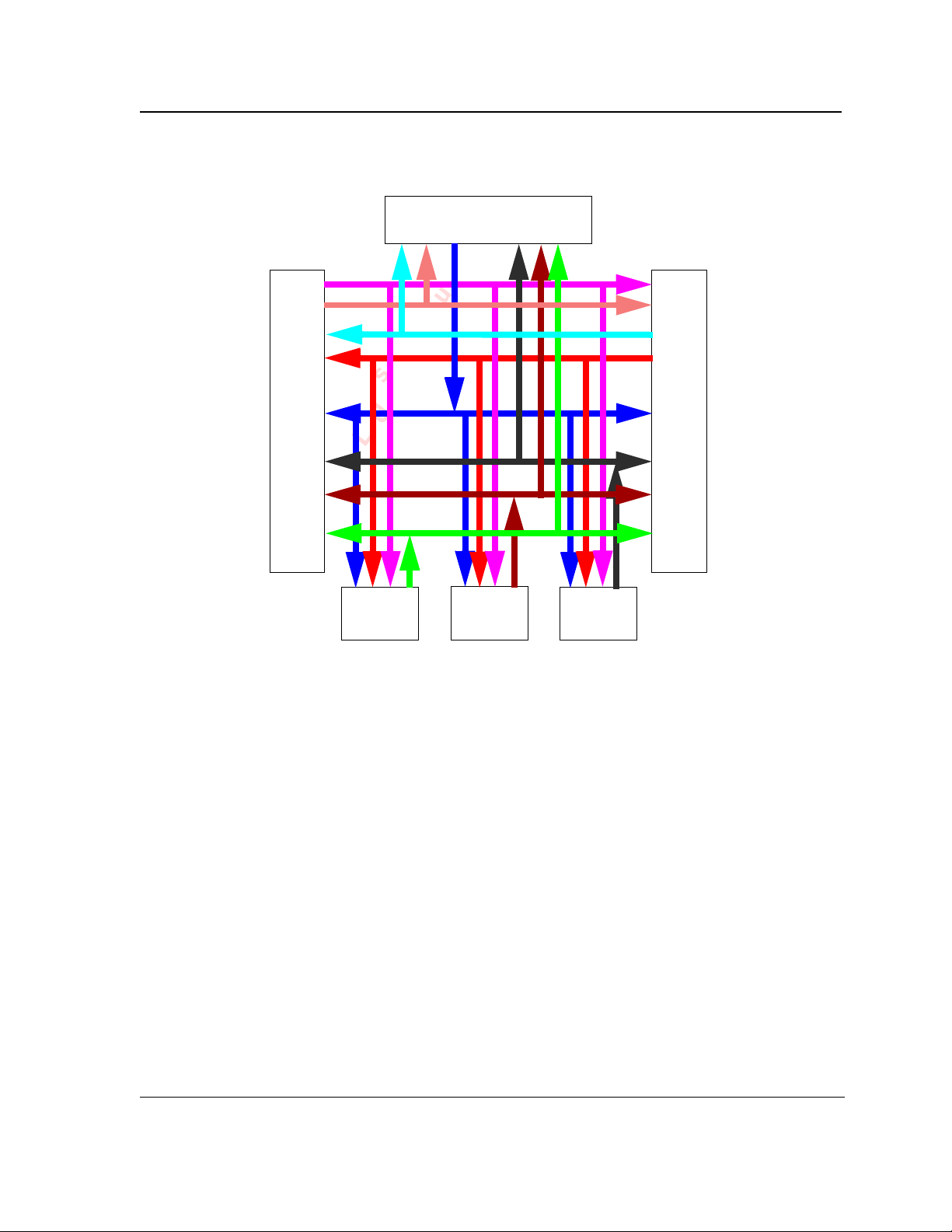
Figure 3-1. PXA300 and PXA310 Processor Memory Switch Block Diagram
Core Subsystem Interface
Memory Switch
System Bus #2
SMC
Interface
DMC
Interface
Internal
SRAM
MARVELL CONFIDENTIAL, UNDER NDA# 12101050
69rlq62d-f714peg4 * Memec (Headquarters) - Unique Tech, Insight, Impact
System Bus #1
MARVELL CONFIDENTIAL - UNAUTHORIZED DISTRIBUTION OR USE STRICTLY PROHIBITED
MARVELL CONFIDENTIAL, UNDER NDA# 12101050
Copyright © 12/13/06 Marvell
December 13, 2006 Document Classification: Proprietary Information Page 63
69rlq62d-f714peg4 * Memec (Headquarters) - Unique Tech, Insight, Impact
Not approved by Document Control. For review only.
CONFIDENTIAL
Doc. No. MV-TBD-00 Rev. A
69rlq62d-f714peg4 * Memec (Headquarters) - Unique Tech, Insight, Impact * UNDER NDA# 12101050
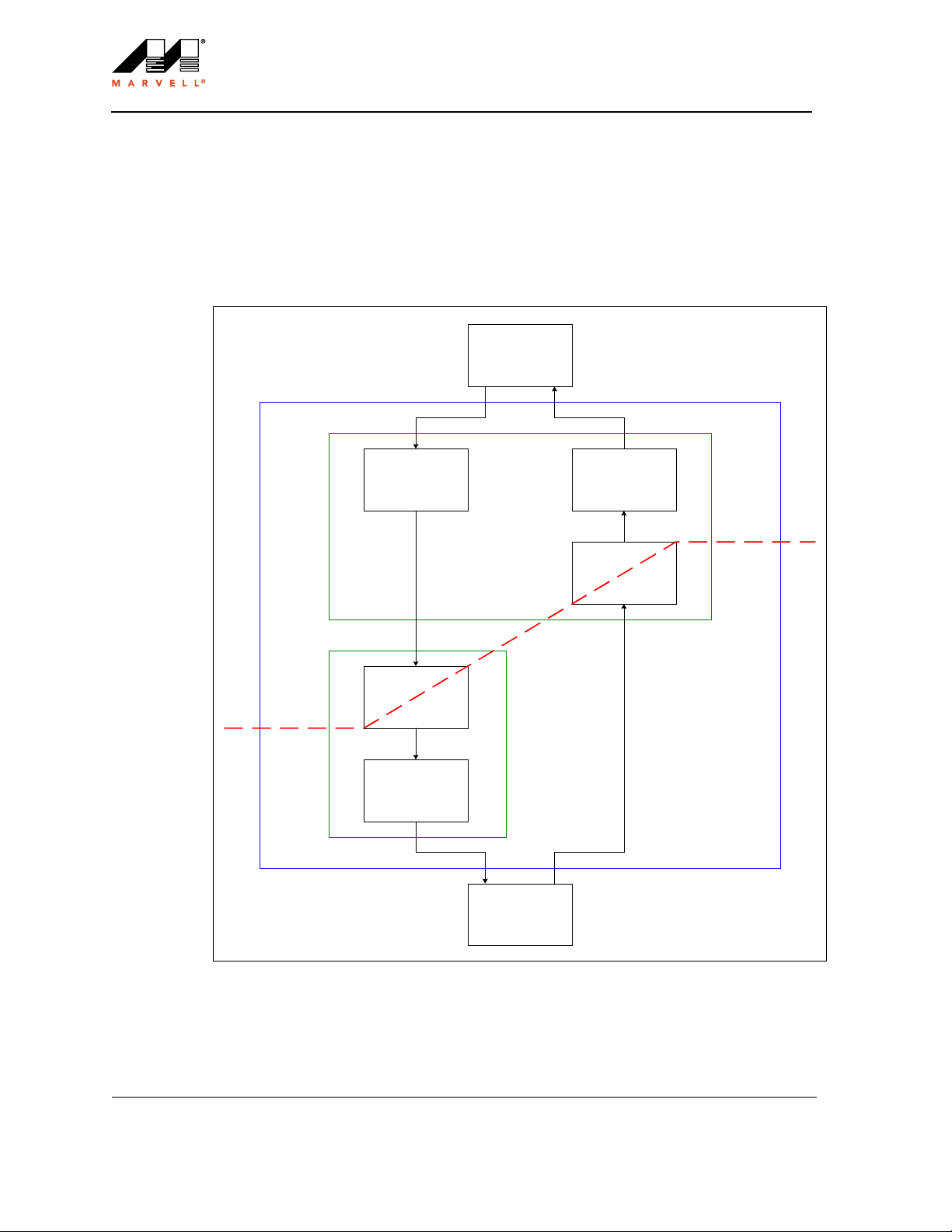
PXA300 Processor and PXA310 Processor
Vol. I: System and Timer Configuration Developers Manual
3.4.2 The Memory Switch Concept
The memory switch bus is responsible for handling the read and write address, data, and related attributes from
the initiators to the completers. Figure 3-1
shows only the path from one initiator to one completer, though many such paths exist within the memory switch
bus. The initiators interfacing with the memory switch bus initiate new read or write transfers.
Figure 3-2. Memory Switch Concept
illustrates the overall concept of the memory switch bus. Figure 3-2
Initiator
Me mory Sw itc h
Bus Protocol and
Demuxing of Address
and Attributes
Initiator Interface
MARVELL CONFIDENTIAL, UNDER NDA# 12101050
Initiator
Clock Domain
Completer
Clock Domain
FIFO and FIFO
Control Logic
Core Subsystem/System Bus #1/System Bus #2
Mux, Arbitration, and
Bus Protocol
FIFO and FIFO
Control Logic
69rlq62d-f714peg4 * Memec (Headquarters) - Unique Tech, Insight, Impact
Mux, Arbitration, and
Simple Bus Protocol
Initiator
Clock Domain
Completer
Clock Domain
MARVELL CONFIDENTIAL - UNAUTHORIZED DISTRIBUTION OR USE STRICTLY PROHIBITED
Com plet er Interfac e
Address, Attributes, WD ata
Completer
RdData, Attributes
Static Ext MemC /
Dynamic Ext MemC /
Intern a l S R A M /
internal Flash /
System Bus #1 /
System Bus #2
MARVELL CONFIDENTIAL, UNDER NDA# 12101050
Doc. No. MV-TBD-00 Rev. A
CONFIDENTIAL
Page 64 Document Classification: Proprietary Information December 13, 2006
69rlq62d-f714peg4 * Memec (Headquarters) - Unique Tech, Insight, Impact
Not approved by Document Control. For review only.
Copyright © 12/13/06 Marvell
69rlq62d-f714peg4 * Memec (Headquarters) - Unique Tech, Insight, Impact * UNDER NDA# 12101050

Pin Descriptions and Control 4
This chapter describes both the PXA300 proc ess or and the PXA310 proces so r log ical sign al s and thei r mappi ng
to physical package pins.
4.1 Overview
The PXA300 processor and the PXA310 processor both feature single-function (dedicated) and multi-function
pins. The pin-control unit manages the configuration of these multi-function pi ns , inclu di ng the selection of
alternate peripheral functions, and controls the pin state during reset and low-power modes for every pin.
The pin-control unit contains registers that allow the reset and low-power mode configuration of each
multi-function pin to hold its last driven output value or instead be forced into one of five states: output driven
high, output driven l ow, output high impedance, input p ul le d h igh, and input pulled low. This register defaults to
an appropriate state at reset or power up but is software-configurable thereafter. The pin unit also contains
registers to configure t he ou t put drive strength of individual pin s when configured as outputs. Many (but not al l)
multi-function pins support configuration as a software-managed GPIO channel, which can be programmed as an
output or an input that can serve as an interrupt sour ce. Many pi ns can also generate wake-up events to bring the
processor out of the S0/D1, S0/D2, S2/D3 and S3/D4 low-power modes.
4.1.1 Differences Between PXA300 and PXA310 Processors
69rlq62d-f714peg4 * Memec (Headquarters) - Unique Tech, Insight, Impact
MARVELL CONFIDENTIAL - UNAUTHORIZED DISTRIBUTION OR USE STRICTLY PROHIBITED
There are two significant differences between PXA300 and PXA310 processors that relate to the external
MARVELL CONFIDENTIAL, UNDER NDA# 12101050
pads/pin connections.
1. PXA300 processor includes a 22-pin UTMI USB 2.0 compliant interface. PXA310 processor replaces the
UTMI interface with a 12-pin UTMI + Low Pin Interface (ULPI).
2. PXA310 processor includes a third MMC/SD/SDIO controller interface.
4.2 Features
This section lists the general features of the pin-control unit.
• Controls the state of pins during reset and low- power modes
• Supports holding last-driven state or register-defined state for all outputs during reset and low-power modes
• Manages selection of GPIO and other alternate peripheral functions
• Supports software configuration of output drive strength
• Supports external interrupt generation and wakeup-event detection.
MARVELL CONFIDENTIAL, UNDER NDA# 12101050
Copyright © 2006 Marvell
December 13, 2006, Preliminary Document Classification: Proprietary Information Page 65
69rlq62d-f714peg4 * Memec (Headquarters) - Unique Tech, Insight, Impact
Not approved by Document Control. For review only.
CONFIDENTIAL
Doc. No. MV-TBD-00 Rev. A
69rlq62d-f714peg4 * Memec (Headquarters) - Unique Tech, Insight, Impact * UNDER NDA# 12101050

PXA300 Processor and PXA310 Processor
Vol. I: System and Timer Configuration Developers Manual
CIR_OUT UART3_RXD
(Wake
MM1_DATA<0>
MARVELL CONFIDENTIAL, UNDER NDA# 12101050
69rlq62d-f714peg4 * Memec (Headquarters) - Unique Tech, Insight, Impact
Alt. FN 1 Alt. FN 2 Alt. FN 3 Alt. FN 4 Alt. FN 5 Alt. FN 6 Alt. FN 7
Primary
Function at
Reset (Alt FN 0)
REN
SMEM_DF_XCV
GPIO_1 nCS<2>
KP_DKIN<6>
U_IO (wake
GPIO_2 nCS<3>
GPIO_3
(Wake
GENERIC[10])
MM1_DATA<1>
KP_DKIN<7>
(wake
U_DETECT
ADxER[19])
(Wake
GENERIC[10])
MM1_DATA<2>
ADxER[19])
GPIO_5 U_CLK KP_MKIN<0>
(Wake
GENERIC[10])
MM1_DAT A<3>
MM1_CMD
GENERIC[10])
(wake
(Wake
GENERIC[10])
GENERIC[11])
MM2_DATA<0>
MM2_DATA<1>
KP_MKIN<6>
ADxER[20])
SC_DETECT
SC_IO (wake
GPIO_9
(wake
KP_MKIN<7>
(wake
(wake
GENERIC[11])
MM2_DATA<2>
ADxER[20])
GPIO_11 SC_CLK KP_MKOUT<5>
(wake
GENERIC[11])
GENERIC[11])
MM2_DATA<3>
GPIO_13 KP_MKOUT<7> MM2_CLK
MARVELL CONFIDENTIAL - UNAUTHORIZED DISTRIBUTION OR USE STRICTLY PROHIBITED
VCC_DF
Table 4-1. PXA300 Processors Alternate Function Table
Pin Name Power Supply
4.3 PXA300 Processors Pin List with Alternate Functions
GPIO0 VCC_DF GPIO_0 RDY
Doc. No. MV-TBD-00 Rev. A
VCC_DF
VCC_CARD1
GPIO1
GPIO2
GPIO3
GPIO4 VCC_CARD1 GPIO_4
VCC_CARD1
MARVELL CONFIDENTIAL, UNDER NDA# 12101050
GPIO5
GPIO6 VCC_CARD1 GPIO_6 U_nRST KP_MKIN<1>
GPIO7 VCC_CARD1 GPIO_7 KP_MKOUT<5> UART3_RXD MM1_CLK UART3_TXD
GPIO8 VCC_CARD1 GPIO_8 UART3_TXD
VCC_CARD2
GPIO9
GPIO10 VCC_CARD2 GPIO_10
CONFIDENTIAL
VCC_CARD2
GPIO11
Copyright © 2006 Marvell
VCC_CARD2
GPIO13
GPIO12 VCC_CARD2 GPIO_12 SC_nRST KP_MKOUT<6>
Page 4-66 Document Classification: Proprietary Information December 13, 2006, Preliminary
69rlq62d-f714peg4 * Memec (Headquarters) - Unique Tech, Insight, Impact
Not approved by Document Control. For review only.
69rlq62d-f714peg4 * Memec (Headquarters) - Unique Tech, Insight, Impact * UNDER NDA# 12101050

SSPTXD1
(wake
EXT_SYNC0
MM1_CMD
(Wake
MM2_CMD
GENERIC[11])
MARVELL CONFIDENTIAL, UNDER NDA# 12101050
(wake
EXT_SYNC1
GENERIC[12])
GENERIC[12])
UART2_TXD UART2_RXD
N_3 (wake
GENERIC[0])
AC97_SDATA_I
N_3 (wake
GENERIC[0])
AC97_SDATA_I
SSPSYSCLK2
SSPSCLK2 UTM_RXACTIVE
U2D_RXERROR
(wake
SSPSFRM2
GENERIC[2])
SSPRXD2 (wake
GENERIC[2])
SSPTXD2 U2D_OPMODE0
U2D_OPMODE1 SSPTXD2
U2D_TXVALID
(wake
SPCLK2EN
GENERIC[2])
SSPRXD2 (wake
GENERIC[2])
SSPEXTCLK2/S
69rlq62d-f714peg4 * Memec (Headquarters) - Unique Tech, Insight, Impact
MARVELL CONFIDENTIAL - UNAUTHORIZED DISTRIBUTION OR USE STRICTLY PROHIBITED
Alt. FN 1 Alt. FN 2 Alt. FN 3 Alt. FN 4 Alt. FN 5 Alt. FN 6 Alt. FN 7
T a ble 4-1. PXA300 Processors Alternate Function Table
Primary
Function at
Pin Name Power Supply
GPIO_14
Reset (Alt FN 0)
VCC_CARD2
GPIO14
Copyright © 2006 Marvell
T
SCL (wake
SDA (wake
GENERIC[9])
GENERIC[9])
AC97_nACRESE
GPIO_21
GPIO_22
GPIO_17 PWM<0> SSPSFRM2
GPIO_16 U_VS0 SSPSFRM CIR_OUT UART2_RTS UART2_CTS KP_DKIN<6>
VCC_IO3
VCC_CARD2
GPIO15 VCC_CARD2 GPIO_15 SC_VS0 L_CS UART2_CTS UART2_RTS MM1_CMD SSPSCLK
GPIO16
GPIO17
GPIO18 VCC_IO3 GPIO_18 PWM<1> SSPRXD
GPIO_19 PWM<2> SSPTXD2 KP_MKOUT<4> UART2_RXD UART2_TXD CHOUT0 SSPRXD2
VCC_IO3
GPIO19
VCC_IO3
GPIO21
GPIO20 VCC_IO3 GPIO_20 PWM<3> SSPTXD KP_MKOUT<5> HZ_CLK ONE_WIRE CHOUT1 SSPRXD
MARVELL CONFIDENTIAL, UNDER NDA# 12101050
GPIO_23
VCC_IO3
VCC_IO3
GPIO22
GPIO23
GPIO_24 AC97_SYSCLK UTM_RXVALID SSPRXD2 SSPTXD2
VCC_IO3
GPIO24
N_0 (Wake
GENERIC[0])
AC97_SDATA_I
GPIO_25
VCC_IO3
GPIO25
GPIO26 VCC_IO3 GPIO_26
CONFIDENTIAL
AC97_SDATA_O
UT
GPIO_28 AC97_SYNC
VCC_IO3
GPIO27 VCC_IO3 GPIO_27
GPIO28
(Wake
GENERIC[0])
AC97_BITCLK
GPIO29 VCC_IO3 GPIO_29
Doc. No. MV-TBD-00 Rev. A
December 13, 2006, Preliminary Document Classification: Proprietary Information Page 67
69rlq62d-f714peg4 * Memec (Headquarters) - Unique Tech, Insight, Impact
Not approved by Document Control. For review only.
69rlq62d-f714peg4 * Memec (Headquarters) - Unique Tech, Insight, Impact * UNDER NDA# 12101050

PXA300 Processor and PXA310 Processor
Vol. I: System and Timer Configuration Developers Manual
OUT5
N5
SSPTXD SSPRXD SSPTXD2
(wake
UART1_DSR
UTM_PHYDATA
GENERIC[3])
U2D_PHYDATAI
UART1_CTS
GENERIC[3])
OUT1
OUT6
OUT7
UTM_PHYDATA
UART1_RTS
UART1_DTR
N6
N7
U2D_PHYDATAI
OUT0
UTM_PHYDATA
UTM_PHYDATA
N1
N0
U2D_PHYDATAI
U2D_PHYDATAI
SSPSCLK SSPSCLK2
(wake
UART1_TXD
UART1_RXD
OUT0
UTM_PHYDATA
MARVELL CONFIDENTIAL, UNDER NDA# 12101050
UART1_RXD
69rlq62d-f714peg4 * Memec (Headquarters) - Unique Tech, Insight, Impact
Alt. FN 1 Alt. FN 2 Alt. FN 3 Alt. FN 4 Alt. FN 5 Alt. FN 6 Alt. FN 7
U2D_PHYDATAI
UTM_PHYDATA
(wake
GENERIC[3])
N0
U2D_PHYDATAI
UART1_RTS
GENERIC[3])
OUT1
OUT2
UTM_PHYDATA
UTM_PHYDATA
(wake
UART1_TXD
UART1_CTS
UART1_DCD
N1
N2
U2D_PHYDATAI
U2D_PHYDATAI
OUT3
N3
UART1_DTR SSPSFRM SSPSFRM2
UTM_PHYDATA
(wake
UART1_DSR
GENERIC[3])
U2D_PHYDATAI
OUT4
N4
SSPRXD SSPTXD SSPRXD2 SSPTXD2
UTM_PHYDATA
(wake
UART1_RI
GENERIC[3])
U2D_PHYDATAI
KP_MKOUT<6>
OUT6
OUT5
OUT4
OUT3
OUT2
UTM_PHYDATA
UTM_PHYDATA
UTM_PHYDATA
UTM_PHYDATA
UTM_PHYDATA
N6
N5
N4
N3
N2
U2D_PHYDATAI
U2D_PHYDATAI
U2D_PHYDATAI
U2D_PHYDATAI
U2D_PHYDATAI
MARVELL CONFIDENTIAL - UNAUTHORIZED DISTRIBUTION OR USE STRICTLY PROHIBITED
Table 4-1. PXA300 Processors Alternate Function Table
Primary
Function at
Pin Name Power Supply
Reset (Alt FN 0)
GPIO_30
VCC_IO3
GPIO30
GPIO31 VCC_IO3 GPIO_31
Doc. No. MV-TBD-00 Rev. A
GPIO_34
VCC_IO3
GPIO32 VCC_IO3 GPIO_32
GPIO33 VCC_IO3 GPIO_33
MARVELL CONFIDENTIAL, UNDER NDA# 12101050
GPIO34
GPIO35 VCC_IO3 GPIO_35
GPIO_36
GPIO_37
VCC_IO3
VCC_IO3
GPIO36
GPIO37
GPIO38 VCC_IO3 GPIO_38 UTM_CLK KP_MKOUT<5>
GPIO_40 CIF_DD<1>
GPIO_39 CIF_DD<0>
VCC_CI
VCC_CI
GPIO40
GPIO39
CONFIDENTIAL
GPIO_42 CIF_DD<3>
VCC_CI
GPIO42
GPIO41 VCC_CI GPIO_41 CIF_DD<2>
Copyright © 2006 Marvell
GPIO_44 CIF_DD<5>
VCC_CI
GPIO45 VCC_CI GPIO_45 CIF_DD<6>
GPIO44
GPIO43 VCC_CI GPIO_43 CIF_DD<4>
Page 4-68 Document Classification: Proprietary Information December 13, 2006, Preliminary
69rlq62d-f714peg4 * Memec (Headquarters) - Unique Tech, Insight, Impact
Not approved by Document Control. For review only.
69rlq62d-f714peg4 * Memec (Headquarters) - Unique Tech, Insight, Impact * UNDER NDA# 12101050

ML_DD<0>
ML_DD<1>
ML_DD<2>
ML_DD<3>
ML_DD<4>
ML_DD<5>
ML_DD<6>
ML_DD<7>
ML_DD<8>
ML_DD<9>
ML_DD<10>
U2D_XCVR_SE
ML_DD<11>
ML_DD<12>
ML_DD<13>
6
LECT
LECT
U2D_TERM_SE
SMEM_FADDR1
7
SMEM_FADDR1
0
1
SMEM_FADDR1
SMEM_FADDR1
SMEM_FADDR1
OUT7
UTM_PHYDATA
N7
MARVELL CONFIDENTIAL, UNDER NDA# 12101050
U2D_PHYDATAI
69rlq62d-f714peg4 * Memec (Headquarters) - Unique Tech, Insight, Impact
Alt. FN 1 Alt. FN 2 Alt. FN 3 Alt. FN 4 Alt. FN 5 Alt. FN 6 Alt. FN 7
Primary
Function at
Reset (Alt FN 0)
GPIO_48 CIF_DD<9> UTM_RXVALID
CIF_MCLK UTM_RXACTIVE CLK_48M GPIO<49>
GPIO_53 UTM_TXREADY KP_MKOUT6
GPIO_54 L_DD<0> SMEM_FADDR4
GPIO_55 L_DD<1> SMEM_FADDR5
GPIO_56 L_DD<2> SMEM_FADDR6
CIF_VSYNC U2D_OPMODE1 GPIO<52>
GPIO_57 L_DD<3> SMEM_FADDR7
GPIO_60 L_DD<6>
GPIO_62 L_DD<8> L_CS
2
3
SMEM_FADDR1
4
SMEM_FADDR1
GPIO_64 L_DD<10> SSPSCLK2
5
SMEM_FADDR1
GPIO_66 L_DD<12> SSPRXD2 U2D_SUSPEND SSPTXD2
SSPRXD2
E0
UTM_LINESTAT
GPIO_67 L_DD<13> SSPTXD2
MARVELL CONFIDENTIAL - UNAUTHORIZED DISTRIBUTION OR USE STRICTLY PROHIBITED
VCC_CI
T a ble 4-1. PXA300 Processors Alternate Function Table
Pin Name Power Supply
GPIO46 VCC_CI CIF_DD<7> GPIO<46>
GPIO47 VCC_CI GPIO_47 CIF_DD<8> UTM_RXACTIVE
Copyright © 2006 Marvell
VCC_CI
GPIO48
GPIO49
VCC_CI
VCC_LCD
VCC_LCD
VCC_LCD
VCC_LCD
VCC_LCD
GPIO50 VCC_CI CIF_PCLK U2D_ERROR GPIO<50>
GPIO51 VCC_CI CIF_HSYNC U2D_OPMODE0 GPIO<51>
GPIO52
GPIO53
GPIO54
GPIO55
GPIO56
GPIO57
MARVELL CONFIDENTIAL, UNDER NDA# 12101050
GPIO58 VCC_LCD GPIO_58 L_DD<4> SMEM_FADDR8
CONFIDENTIAL
GPIO59 VCC_LCD GPIO_59 L_DD<5> SMEM_FADDR9
VCC_LCD
GPIO60
GPIO61 VCC_LCD GPIO_61 L_DD<7>
VCC_LCD
GPIO62
GPIO63 VCC_LCD GPIO_63 L_DD<9> L_VSYNC
VCC_LCD
GPIO64
Doc. No. MV-TBD-00 Rev. A
VCC_LCD
VCC_LCD
GPIO65 VCC_LCD GPIO_65 L_DD<11> SSPSFRM2
GPIO66
GPIO67
December 13, 2006, Preliminary Document Classification: Proprietary Information Page 69
69rlq62d-f714peg4 * Memec (Headquarters) - Unique Tech, Insight, Impact
Not approved by Document Control. For review only.
69rlq62d-f714peg4 * Memec (Headquarters) - Unique Tech, Insight, Impact * UNDER NDA# 12101050

PXA300 Processor and PXA310 Processor
Vol. I: System and Timer Configuration Developers Manual
ML_DD<14>
8
SMEM_FADDR1
E1
UTM_LINESTAT
ML_DD<15>
9
SMEM_FADDR1
U2D_TXVALID
GENERIC[7])
SSPRXD3 (wake
0
SMEM_FADDR2
SSPTXD3
1
SMEM_FADDR2
KP_MKIN<7>
ML_FCLK
2
SMEM_FADDR2
ML_LCLK
3
SMEM_FADDR2
ML_PCLK
4
SMEM_FADDR2
ML_BIAS
5
SMEM_FADDR2
0>
MSL1_OB_DAT<
MSL1_IB_DAT
(wake
MM2_DATA<0>
UART1_TXD
KP_MKOUT<7> MSL1_OB_CLK KP_MKOUT<6>
(wake
GENERIC[11])
MM2_DATA<1>
MSL1_IB_STB MSL1_OB_STB
GENERIC[11])
MM2_DATA<2>/
MM2_CS0 (wake
UART1_RTS
(Wake
MSL1_OB_WAIT
MSL1_IB_WAIT
GENERIC[11])
MM2_DATA<3>/
MM2_CS1 (wake
0> (Wake
ADxER[24])
MSL1_IB_DAT<
MSL1_OB_DAT<
GENERIC[11])
UART1_DTR MM2_CLK
(Wake
ADxER[24])
0>
ADxER[24])
MSL1_IB_CLK
MSL1_OB_CLK
(Wake
MM2_CMD
GENERIC[11])
69rlq62d-f714peg4 * Memec (Headquarters) - Unique Tech, Insight, Impact
MARVELL CONFIDENTIAL - UNAUTHORIZED DISTRIBUTION OR USE STRICTLY PROHIBITED
(wake
(wake
SSPSFRM3
GENERIC[7])
GPIO_68 L_DD<14>
VCC_LCD
GPIO68
GPIO69 VCC_LCD GPIO_69 L_DD<15>
Table 4-1. PXA300 Processors Alternate Function Table
MARVELL CONFIDENTIAL, UNDER NDA# 12101050
SSPSCLK3
Alt. FN 1 Alt. FN 2 Alt. FN 3 Alt. FN 4 Alt. FN 5 Alt. FN 6 Alt. FN 7
Primary
Function at
Reset (Alt FN 0)
Pin Name Power Supply
Doc. No. MV-TBD-00 Rev. A
(wake
USB_P3_1
GENERIC[7])
GENERIC[7])
SSPRXD3 (wake
GPIO_71 L_DD<17>
VCC_LCD
GPIO70 VCC_LCD GPIO_70 L_DD<16> SSPTXD3 KP_MKIN<6>
GPIO71
GPIO_73 L_LCLK_A0
VCC_LCD
GPIO72 VCC_LCD GPIO_72 L_FCLK_RD
GPIO73
GPIO_75 L_BIAS
GPIO_76 U2D_RESET L_VSYNC
VCC_LCD
MARVELL CONFIDENTIAL, UNDER NDA# 12101050
GPIO74 VCC_LCD GPIO_74 L_PCLK_WR
GPIO75
GPIO76
ADxER[23])
(wake
UART1_RXD
GENERIC[3])
GPIO_77
VCC_LCD
VCC_MSL
GPIO77
GPIO78 VCC_MSL GPIO_78 UART1_TXD USB_P3_2 UART1_RXD
CONFIDENTIAL
(wake
USB_P3_3
GPIO_79 UART1_CTS
VCC_MSL
GPIO79
USB_P3_4
ADxER[23])
(wake
UART1_DCD
GPIO80 VCC_MSL GPIO_80
Copyright © 2006 Marvell
(wake
USB_P3_5
(wake
UART1_DSR
GENERIC[3])
GPIO_81
VCC_MSL
GPIO81
USB_P3_6
ADxER[23])
(wake
UART1_RI
GENERIC[3])
GENERIC[3])
GPIO82 VCC_MSL GPIO_82
Page 4-70 Document Classification: Proprietary Information December 13, 2006, Preliminary
69rlq62d-f714peg4 * Memec (Headquarters) - Unique Tech, Insight, Impact
Not approved by Document Control. For review only.
69rlq62d-f714peg4 * Memec (Headquarters) - Unique Tech, Insight, Impact * UNDER NDA# 12101050

3>
1>
MSL1_IB_DAT<
MSL1_OB_DAT<
MSL1_IB_STB
(Wake
ADxER[24])
1>
MSL1_OB_DAT<
U2D_TXVALID
1> (Wake
MSL1_IB_DAT<
(wake
KP_DKIN<0>
2>
GENERIC[1])
MSL1_OB_DAT<
ADxER[24])
MSL1_IB_DAT<
ADxER[21])
KP_DKIN<1>
SSPRXD (wake
UTM_RXVALID
2> (Wake
(wake
3> (Wake
ADxER[24])
ADxER[21])
ADxER[24])
MSL1_IB_DAT<
KP_DKIN<2>
MSL1_OB_DAT<
(wake
ADxER[21])
KP_DKIN<3>
MSL1_IB_DAT<
UTM_RXACTIVE SSPTXD
1>
MSL1_OB_DAT<
(wake
ADxER[21])
MARVELL CONFIDENTIAL, UNDER NDA# 12101050
KP_MKOUT<0>
KP_MKOUT<1>
KP_MKOUT<3>
2>
U2D_RXERROR
2>
MSL1_OB_DAT<
MSL1_IB_DAT<
SC_nVS1
U2D_OPMODE0
3>
3>
UART3_RTS
(wake
UART3_CTS
GENERIC[5])
GENERIC[7])
SSPRXD3 (wake
(wake
UART3_CTS
UTM_LINESTAT
UART3_RTS
E0
(wake
E1
UART3_TXD SSPTXD3
GENERIC[5])
LECT
U2D_XCVR_SE
(wake
UART3_RXD
U2D_RESET
GENERIC[5])
UART3_RXD
GENERIC[5])
UTM_LINESTAT
69rlq62d-f714peg4 * Memec (Headquarters) - Unique Tech, Insight, Impact
MARVELL CONFIDENTIAL - UNAUTHORIZED DISTRIBUTION OR USE STRICTLY PROHIBITED
Alt. FN 1 Alt. FN 2 Alt. FN 3 Alt. FN 4 Alt. FN 5 Alt. FN 6 Alt. FN 7
T a ble 4-1. PXA300 Processors Alternate Function Table
Primary
Function at
Pin Name Power Supply
GPIO_83 UART1_DTR UART1_DSR MSL1_OB_STB KP_DKIN<2>
Reset (Alt FN 0)
VCC_MSL
GPIO83
Copyright © 2006 Marvell
(wake
SSPSCLK
GPIO85 VCC_MSL GPIO_85
GPIO84 VCC_MSL GPIO_84 UART1_RTS UART1_CTS MSL1_OB_WAIT KP_DKIN<1> MSL1_IB_WAIT
(wake
SSPSFRM
GENERIC[1])
GENERIC[1])
GPIO_86
VCC_MSL
GPIO86
GPIO87 VCC_MSL GPIO_87 SSPTXD KP_MKOUT<2>
GENERIC[1])
SSPRXD (wake
GPIO_88
VCC_MSL
GPIO88
MARVELL CONFIDENTIAL, UNDER NDA# 12101050
SSPEXTCLK/SS
GENERIC[1])
PCLKEN (wake
GPIO89 VCC_MSL GPIO_89
CONFIDENTIAL
(wake
SSPSCLK3
GPIO90 VCC_MSL GPIO_90 SSPSYSCLK SC_nVS2
GPIO91 VCC_IO1 GPIO_91
(wake
SSPSFRM3
GENERIC[7])
GENERIC[7])
GPIO_92
VCC_IO1
GPIO92
GPIO93 VCC_IO1 GPIO_93 SSPTXD3 UART3_TXD
SSPRXD3 (wake
GPIO_94
VCC_IO1
GPIO94
(wake
SSPSCLK4
GENERIC[7])
GPIO95 VCC_IO1 GPIO_95
(wake
SSPSFRM4
GENERIC[8])
GENERIC[8])
GPIO_96
VCC_IO1
GPIO96
Doc. No. MV-TBD-00 Rev. A
December 13, 2006, Preliminary Document Classification: Proprietary Information Page 71
69rlq62d-f714peg4 * Memec (Headquarters) - Unique Tech, Insight, Impact
Not approved by Document Control. For review only.
69rlq62d-f714peg4 * Memec (Headquarters) - Unique Tech, Insight, Impact * UNDER NDA# 12101050

PXA300 Processor and PXA310 Processor
Vol. I: System and Timer Configuration Developers Manual
KP_MKIN<6>
(wake
UART1_TXD
UART1_RXD
GENERIC[3])
SSPTXD4
GENERIC[8])
SSPRXD4 (wake
ECT
U2D_TERMSEL
MARVELL CONFIDENTIAL, UNDER NDA# 12101050
U2D_SUSPEND
LECT
U2D_TERM_SE
M
USB_P2_2 USB_P2_5 USB_P2_6
(wake
UART1_RTS KP_MKIN<7>
UART1_RXD
LECT
U2D_XCVR_SE
U2D_TERM_SE
USB_P2_4 UART1_TXD
UART1_DTR
GENERIC[3])
LECT
KP_MKOUT<6>
(wake
UART1_RXD
M
U2D_SUSPEND
UTM_LINESTAT
USB_P2_8
USB_P2_3
E0
(wake
UART1_DSR
GENERIC[3])
KP_MKOUT<7>
GENERIC[3])
E1
UTM_LINESTAT
E0
UTM_LINESTAT
(wake
(wake
UART3_CTS
UART3_RTS
(wake
ADxER[21])
KP_DKIN<0>
KP_DKIN<1>
UART3_RXD
GENERIC[5])
(wake
(wake
ADxER[21])
KP_DKIN<2>
UART3_TXD U2D_OPMODE1
GENERIC[5])
(wake
ADxER[21])
ADxER[21])
KP_DKIN<3>
69rlq62d-f714peg4 * Memec (Headquarters) - Unique Tech, Insight, Impact
MARVELL CONFIDENTIAL - UNAUTHORIZED DISTRIBUTION OR USE STRICTLY PROHIBITED
Table 4-1. PXA300 Processors Alternate Function Table
Alt. FN 1 Alt. FN 2 Alt. FN 3 Alt. FN 4 Alt. FN 5 Alt. FN 6 Alt. FN 7
Primary
Function at
Reset (Alt FN 0)
Pin Name Power Supply
GPIO97 VCC_IO1 GPIO_97 SSPTXD4
SSPRXD4 (wake
GPIO_98
VCC_IO1
GPIO98
GENERIC[8])
Doc. No. MV-TBD-00 Rev. A
(wake
UART1_RXD
GPIO_99
VCC_IO1
GPIO99
(wake
GENERIC[3])
GPIO100 VCC_IO1 GPIO_100 UART1_TXD USB_P2_6 U2D_RESET USB_P2_2 USB_P2_5
UART1_DCD
GPIO101 VCC_IO1 GPIO_101 UART1_CTS USB_P2_1
GPIO102 VCC_IO1 GPIO_102
CONFIDENTIAL
(wake
UART1_DSR
GENERIC[3])
GPIO_103
VCC_IO1
MARVELL CONFIDENTIAL, UNDER NDA# 12101050
GPIO103
(wake
UART1_RI
GENERIC[3])
GENERIC[3])
GPIO_105 UART1_DTR USB_P2_5
VCC_IO1
GPIO104 VCC_IO1 GPIO_104
GPIO105
(wake
UART3_CTS
GENERIC[5])
GPIO_106 UART1_RTS USB_P2_7 U2D_OPMODE1 UART1_CTS
GPIO_107
VCC_IO1
VCC_IO1
GPIO106
GPIO107
GPIO_108 UART3_RTS
VCC_IO1
GPIO109 VCC_IO1 GPIO_109 UART3_TXD
GPIO108
Copyright © 2006 Marvell
(wake
UART3_RXD
GPIO_110
VCC_IO1
GPIO110
GENERIC[5])
Page 4-72 Document Classification: Proprietary Information December 13, 2006, Preliminary
69rlq62d-f714peg4 * Memec (Headquarters) - Unique Tech, Insight, Impact
Not approved by Document Control. For review only.
69rlq62d-f714peg4 * Memec (Headquarters) - Unique Tech, Insight, Impact * UNDER NDA# 12101050

KP_MKIN<7>
(wake
UART2_CTS
(wake
MARVELL CONFIDENTIAL, UNDER NDA# 12101050
KP_DKIN<4>
69rlq62d-f714peg4 * Memec (Headquarters) - Unique Tech, Insight, Impact
Alt. FN 1 Alt. FN 2 Alt. FN 3 Alt. FN 4 Alt. FN 5 Alt. FN 6 Alt. FN 7
Primary
Function at
GPIO_111 UART2_RTS
Reset (Alt FN 0)
VCC_IO1
UART2_TXD KP_MKIN<6>
GENERIC[4])
(wake
ADxER[21])
KP_DKIN<5>
(wake
UART2_RXD
(wake
UART2_RXD
(wake
ADxER[21])
KP_DKIN<6>
GENERIC[4])
GPIO_113 UART2_TXD
VCC_IO1
UART2_RTS
GENERIC[4])
(wake
ADxER[21])
KP_DKIN<7>
(wake
UART2_CTS
(wake
ADxER[21])
KP_DKIN<0>
(wake
GENERIC[4])
KP_MKIN<0>
GPIO_115
VCC_IO1
(wake
ADxER[21])
KP_DKIN<1>
GENERIC[6])
KP_MKIN<1>
(wake
ADxER[21])
KP_DKIN<2>
(wake
(wake
GENERIC[6])
KP_MKIN<2>
GPIO_117
VCC_IO1
(wake
ADxER[21])
KP_DKIN<3>
GENERIC[6])
KP_MKIN<3>
(wake
ADxER[21])
(wake
GENERIC[6])
ADxER[21])
KP_DKIN<4>
(wake
GENERIC[6])
KP_MKIN<4>
GPIO_119
VCC_IO1
(wake
KP_DKIN<5>
(wake
KP_MKIN<5>
(wake
ADxER[21])
KP_DKIN<6>
GENERIC[6])
GPIO_121 KP_MKOUT<0>
VCC_IO1
(wake
ADxER[21])
KP_DKIN<5>
(wake
ADxER[21])
ADxER[21])
KP_DKIN<4>
GPIO_123 KP_MKOUT<2>
VCC_IO1
MARVELL CONFIDENTIAL - UNAUTHORIZED DISTRIBUTION OR USE STRICTLY PROHIBITED
T a ble 4-1. PXA300 Processors Alternate Function Table
Pin Name Power Supply
GPIO111
Copyright © 2006 Marvell
GPIO112 VCC_IO1 GPIO_112
GPIO113
GPIO114 VCC_IO1 GPIO_114
GPIO115
GPIO116 VCC_IO1 GPIO_116
MARVELL CONFIDENTIAL, UNDER NDA# 12101050
GPIO117
CONFIDENTIAL
GPIO118 VCC_IO1 GPIO_118
GPIO119
GPIO120 VCC_IO1 GPIO_120
GPIO121
GPIO122 VCC_IO1 GPIO_122 KP_MKOUT<1>
GPIO123
Doc. No. MV-TBD-00 Rev. A
December 13, 2006, Preliminary Document Classification: Proprietary Information Page 73
69rlq62d-f714peg4 * Memec (Headquarters) - Unique Tech, Insight, Impact
Not approved by Document Control. For review only.
69rlq62d-f714peg4 * Memec (Headquarters) - Unique Tech, Insight, Impact * UNDER NDA# 12101050

PXA300 Processor and PXA310 Processor
Vol. I: System and Timer Configuration Developers Manual
KP_MKOUT<7>
69rlq62d-f714peg4 * Memec (Headquarters) - Unique Tech, Insight, Impact
MARVELL CONFIDENTIAL - UNAUTHORIZED DISTRIBUTION OR USE STRICTLY PROHIBITED
GENERIC[13])
CLK_EXT (wake
(wake
MARVELL CONFIDENTIAL, UNDER NDA# 12101050
KP_DKIN<3>
Alt. FN 1 Alt. FN 2 Alt. FN 3 Alt. FN 4 Alt. FN 5 Alt. FN 6 Alt. FN 7
Primary
Function at
Reset (Alt FN 0)
Table 4-1. PXA300 Processors Alternate Function Table
Pin Name Power Supply
Doc. No. MV-TBD-00 Rev. A
Page 4-74 Document Classification: Proprietary Information December 13, 2006, Preliminary
(wake
ADxER[21])
GPIO_124 KP_MKOUT<3>
VCC_IO1
GPIO124
ADxER[21])
KP_DKIN<2>
GPIO125 VCC_IO1 GPIO_125 KP_MKOUT<4>
GPIO126 VCC_IO1 GPIO_126 HZ_CLK ONE_WIRE
(wake
KP_DKIN<0>
GPIO0_2 USBHPEN
GPIO_127 LCD_CS KP_DKIN<0>
VCC_IO1
VCC_IO1
GPIO127
GPIO0_2
69rlq62d-f714peg4 * Memec (Headquarters) - Unique Tech, Insight, Impact
Not approved by Document Control. For review only.
(wake
ADxER[21])
ADxER[21])
KP_DKIN<1>
KP_MKIN[6]
GPIO2_2
VCC_IO3
MARVELL CONFIDENTIAL, UNDER NDA# 12101050
GPIO2_2
GPIO1_2 VCC_IO1 GPIO1_2 USBHPWR
GPIO3_2 VCC_IO3 GPIO3_2 KP_MKIN[7]
CONFIDENTIAL
KP_MKOUT[6] KP_DKIN[0]
GPIO4_2 KP_MKOUT[5]
GPIO5_2
VCC_IO3
VCC_IO3
GPIO4_2
GPIO5_2
GPIO6_2 VCC_IO3 GPIO6_2 KP_MKOUT[7]
Copyright © 2006 Marvell
69rlq62d-f714peg4 * Memec (Headquarters) - Unique Tech, Insight, Impact * UNDER NDA# 12101050

(wake
UART3_RXD
CIR_OUT
GENERIC[5])
(Wake
GENERIC[10])
MM1_DATA<0>
MARVELL CONFIDENTIAL, UNDER NDA# 12101050
REN
SMEM_DF_XCV
69rlq62d-f714peg4 * Memec (Headquarters) - Unique Tech, Insight, Impact
Alt. FN 1 Alt. FN 2 Alt. FN 3 Alt. FN 4 Alt. FN 5 Alt. FN 6 Alt. FN 7
GPIO_0 RDY
Primary
Function at
Reset (Alt FN 0)
GPIO_1 nCS<2>
(wake
ADxER[21])
KP_DKIN<6>
ADxER[19])
U_IO (wake
GPIO_3
(Wake
GENERIC[10])
MM1_DATA<1>
(wake
ADxER[21])
KP_DKIN<7>
(wake
U_DETECT
ADxER[19])
GPIO_4
(Wake
GENERIC[10])
MM1_DATA<2>
(wake
GENERIC[6])
KP_MKIN<0>
GPIO_5 U_CLK
(Wake
GENERIC[10])
MM1_DAT A<3>
(wake
GENERIC[6])
KP_MKIN<1>
GPIO_6 U_nRST
MM1_CLK UART3_TXD
(wake
UART3_RXD
(Wake
MM1_CMD
GENERIC[5])
GPIO_8 UART3_TXD
(wake
GENERIC[10])
GENERIC[11])
MM2_DATA<0>
(wake
GENERIC[6])
KP_MKIN<6>
ADxER[20])
SC_IO (wake
MARVELL CONFIDENTIAL - UNAUTHORIZED DISTRIBUTION OR USE STRICTLY PROHIBITED
VCC_DF
Table 4-2. PXA310 Processor Alternate Function Table
Pin Name Power Supply
4.4 PXA310 Processor Pin List with Alternate Functions
Copyright © 2006 Marvell
VCC_DF
GPIO0
GPIO1
GPIO2 VCC_DF GPIO_2 nCS<3>
VCC_CARD1
GPIO3
CONFIDENTIAL
VCC_CARD1
GPIO4
MARVELL CONFIDENTIAL, UNDER NDA# 12101050
VCC_CARD1
GPIO5
VCC_CARD1
GPIO6
GPIO7 VCC_CARD1 GPIO_7 KP_MKOUT<5>
VCC_CARD1
GPIO8
GPIO9 VCC_CARD2 GPIO_9
Doc. No. MV-TBD-00 Rev. A
December 13, 2006, Preliminary Document Classification: Proprietary Information Page 75
69rlq62d-f714peg4 * Memec (Headquarters) - Unique Tech, Insight, Impact
Not approved by Document Control. For review only.
69rlq62d-f714peg4 * Memec (Headquarters) - Unique Tech, Insight, Impact * UNDER NDA# 12101050

PXA300 Processor and PXA310 Processor
Vol. I: System and Timer Configuration Developers Manual
SSPTXD
(wake
SSPSCLK
(Wake
MM1_CMD
(wake
GENERIC[11])
MM2_DATA<1>
(wake
GENERIC[6])
KP_MKIN<7>
(wake
GENERIC[11])
MM2_DATA<2>
(wake
GENERIC[11])
MM2_DATA<3>
MM2_CMD
MM1_CMD
GENERIC[10])
(Wake
GENERIC[11])
UART2_CTS
(wake
GENERIC[1])
KP_DKIN<6>
(wake
(Wake
UART2_CTS
GENERIC[10])
UART2_RTS
(wake
CIR_OUT UART2_RTS
GENERIC[4])
(wake
ADxER[21])
EXT_SYNC0
GENERIC[4])
(wake
EXT_SYNC1
(wake
UART2_RXD
UART2_TXD
N_3 (wake
AC97_SDATA_I
GENERIC[12])
GENERIC[4])
GENERIC[0])
GENERIC[12])
SSPRXD2 (wake
UART2_TXD CHOUT0
(wake
UART2_RXD
GENERIC[2])
GENERIC[1])
SSPRXD (wake
GENERIC[4])
69rlq62d-f714peg4 * Memec (Headquarters) - Unique Tech, Insight, Impact
MARVELL CONFIDENTIAL - UNAUTHORIZED DISTRIBUTION OR USE STRICTLY PROHIBITED
MARVELL CONFIDENTIAL, UNDER NDA# 12101050
Alt. FN 1 Alt. FN 2 Alt. FN 3 Alt. FN 4 Alt. FN 5 Alt. FN 6 Alt. FN 7
Primary
Function at
Reset (Alt FN 0)
Table 4-2. PXA310 Processor Alternate Function Table
Pin Name Power Supply
Doc. No. MV-TBD-00 Rev. A
(wake
ADxER[20])
SC_DETECT
GPIO10 VCC_CARD2 GPIO_10
(wake
SSPSFRM
GPIO_13 KP_MKOUT<7> MM2_CLK
GPIO_14
VCC_CARD2
VCC_CARD2
MARVELL CONFIDENTIAL, UNDER NDA# 12101050
GPIO13
GPIO11 VCC_CARD2 GPIO_11 SC_CLK KP_MKOUT<5>
GPIO12 VCC_CARD2 GPIO_12 SC_nRST KP_MKOUT<6>
GPIO14
GPIO15 VCC_CARD2 GPIO_15 SC_VS0 L_CS
GPIO_16 U_VS0
VCC_CARD2
GPIO16
CONFIDENTIAL
(wake
SSPSFRM2
GENERIC[1])
GENERIC[2])
GPIO17 VCC_IO3 GPIO_17 PWM<0>
GENERIC[1])
SSPRXD (wake
SCL (wake
GENERIC[9])
GPIO_18 PWM<1>
VCC_IO3
GPIO18
GPIO_19 PWM<2> SSPTXD2 KP_MKOUT<4>
GPIO_20 PWM<3> SSPTXD KP_MKOUT<5> HZ_CLK ONE_WIRE CHOUT1
VCC_IO3
VCC_IO3
GPIO19
GPIO20
GPIO21 VCC_IO3 GPIO_21
Copyright © 2006 Marvell
Page 4-76 Document Classification: Proprietary Information December 13, 2006, Preliminary
69rlq62d-f714peg4 * Memec (Headquarters) - Unique Tech, Insight, Impact
Not approved by Document Control. For review only.
69rlq62d-f714peg4 * Memec (Headquarters) - Unique Tech, Insight, Impact * UNDER NDA# 12101050

SSPTXD2
SSPRXD2 (wake
SSPTXD2
GENERIC[2])
SSPRXD2 (wake
(wake
GENERIC[2])
UART1_TXD
UART1_RXD
UART1_RTS
GENERIC[3])
(Wake
ADxER[26])
MMC1_CMD
MARVELL CONFIDENTIAL, UNDER NDA# 12101050
69rlq62d-f714peg4 * Memec (Headquarters) - Unique Tech, Insight, Impact
Alt. FN 1 Alt. FN 2 Alt. FN 3 Alt. FN 4 Alt. FN 5 Alt. FN 6 Alt. FN 7
Primary
Function at
Reset (Alt FN 0)
N_3 (wake
GENERIC[0])
AC97_SDATA_I
SDA (wake
GPIO_22
VCC_IO3
SSPSYSCLK2 MMC_CLK
T
GENERIC[9])
AC97_nACRESE
GPIO_24 AC97_SYSCLK
GPIO_23
VCC_IO3
VCC_IO3
(wake
SSPSCLK2
N_0 (Wake
AC97_SDATA_I
GPIO_25
VCC_IO3
(wake
SSPSFRM2
GENERIC[2])
GENERIC[0])
SSPTXD2
GENERIC[2])
SSPRXD2 (wake
UT
AC97_SDATA_O
GPIO_28 AC97_SYNC
VCC_IO3
(Wake
GENERIC[10])
MM1_DATA<0>
SPCLK2EN
GENERIC[2])
SSPEXTCLK2/S
(Wake
AC97_BITCLK
ULPI_DATA_OU
(wake
GENERIC[2])
GENERIC[0])
T0
(wake
UART1_RXD
T1
ULPI_DATA_OU
(wake
ADxER[26])
UART1_TXD
(wake
USB_P2_6
ADxER[22])
(wake
ADxER[26])
GENERIC[3])
T2
ULPI_DATA_OU
(wake
UART1_CTS
GENERIC[3])
(wake
USB_P2_4
ADxER[22])
GPIO_32
VCC_ULPI
MARVELL CONFIDENTIAL - UNAUTHORIZED DISTRIBUTION OR USE STRICTLY PROHIBITED
Table 4-2. PXA310 Processor Alternate Function Table
Pin Name Power Supply
GPIO22
Copyright © 2006 Marvell
GPIO24
GPIO23
GPIO25
MARVELL CONFIDENTIAL, UNDER NDA# 12101050
GPIO27 VCC_IO3 GPIO_27
GPIO26 VCC_IO3 GPIO_26
GPIO28
GPIO29 VCC_IO3 GPIO_29
GPIO30 VCC_ULPI GPIO_30 USB_P2_2
CONFIDENTIAL
GPIO31 VCC_ULPI GPIO_31
Doc. No. MV-TBD-00 Rev. A
GPIO32
December 13, 2006, Preliminary Document Classification: Proprietary Information Page 77
69rlq62d-f714peg4 * Memec (Headquarters) - Unique Tech, Insight, Impact
Not approved by Document Control. For review only.
69rlq62d-f714peg4 * Memec (Headquarters) - Unique Tech, Insight, Impact * UNDER NDA# 12101050

PXA300 Processor and PXA310 Processor
Vol. I: System and Timer Configuration Developers Manual
ULPI_DATA_OU
SSPSCLK2
SSPSCLK
ULPI_OTG_INT
T3
SSPTXD2
(wake
(wake
R (wake
(wake
(wake
SSPSFRM2
GENERIC[2])
GENERIC[1])
GENERIC[3])
ADxER[26])
GENERIC[2])
SSPRXD2 (wake
(wake
SSPSFRM
ULPI_DATA_OU
SSPTXD
GENERIC[1])
UART1_DTR
SSPRXD (wake
T4
ULPI_DATA_OU
GENERIC[2])
GENERIC[1])
T5
SSPTXD2
SSPRXD (wake
SSPTXD
(wake
UART1_DSR
ULPI_DATA_OU
GENERIC[1])
T6
KP_MKOUT<5>
(wake
UART1_CTS
GENERIC[3])
GENERIC[3])
T7
ULPI_DATA_OU
69rlq62d-f714peg4 * Memec (Headquarters) - Unique Tech, Insight, Impact
MARVELL CONFIDENTIAL - UNAUTHORIZED DISTRIBUTION OR USE STRICTLY PROHIBITED
(wake
MARVELL CONFIDENTIAL, UNDER NDA# 12101050
UART1_DCD
R
(wake
ULPI_OTG_INT
GPIO33 VCC_ULPI GPIO_33
Table 4-2. PXA310 Processor Alternate Function Table
Alt. FN 1 Alt. FN 2 Alt. FN 3 Alt. FN 4 Alt. FN 5 Alt. FN 6 Alt. FN 7
Primary
Function at
Reset (Alt FN 0)
Pin Name Power Supply
Doc. No. MV-TBD-00 Rev. A
(wake
(wake
GENERIC[3])
ADxER[22])
GENERIC[3])
(wake
USB_P2_5
(wake
USB_P2_3
ADxER[22])
GPIO_34
VCC_ULPI
GPIO34
GPIO35 VCC_ULPI GPIO_35
UART1_RI
UART1_DSR
UART1_DTR
GENERIC[3])
(wake
USB_P2_1
ADxER[22])
ADxER[22])
GPIO_36
VCC_ULPI
GPIO36
CONFIDENTIAL
ADxER[26])
UPLI_CLK (wake
GPIO_44 CIF_DD<5>
GPIO_45 CIF_DD<6>
GPIO_47 CIF_DD<8>
GPIO_40 CIF_DD<1>
GPIO_41 CIF_DD<2>
VCC_CI GPIO_43 CIF_DD<4>
VCC_CI
VCC_CI
VCC_CI
MARVELL CONFIDENTIAL, UNDER NDA# 12101050
GPIO37 VCC_ULPI GPIO_37 UART1_RTS
GPIO38 VCC_ULPI GPIO_38
GPIO39 VCC_CI GPIO_39 CIF_DD<0>
GPIO40
GPIO41
GPIO42 VCC_CI GPIO_42 CIF_DD<3>
GPIO43
VCC_CI
GPIO44
GPIO45
GPIO_48 CIF_DD<9>
VCC_CI
VCC_CI
GPIO46 VCC_CI CIF_DD<7> GPIO<46>
GPIO47
GPIO48
GPIO49 VCC_CI CIF_MCLK CLK_48M GPIO<49>
GPIO50 VCC_CI CIF_PCLK GPIO<50>
CIF_VSYNC GPIO<52>
CIF_HSYNC GPIO<51>
VCC_CI
VCC_CI
GPIO51
GPIO52
Copyright © 2006 Marvell
Page 4-78 Document Classification: Proprietary Information December 13, 2006, Preliminary
69rlq62d-f714peg4 * Memec (Headquarters) - Unique Tech, Insight, Impact
Not approved by Document Control. For review only.
69rlq62d-f714peg4 * Memec (Headquarters) - Unique Tech, Insight, Impact * UNDER NDA# 12101050

ML_DD<0>
ML_DD<1>
ML_DD<2>
ML_DD<3>
ML_DD<4>
ML_DD<5>
ML_DD<6>
ML_DD<7>
ML_DD<8>
ML_DD<9>
ML_DD<10>
ML_DD<11>
ML_DD<12>
2
SMEM_FADDR1
ML_DD<13>
3
SMEM_FADDR1
ML_DD<14>
ML_DD<15>
SSPTXD3
GENERIC[7])
SSPRXD3 (wake
0
SMEM_FADDR1
MARVELL CONFIDENTIAL, UNDER NDA# 12101050
69rlq62d-f714peg4 * Memec (Headquarters) - Unique Tech, Insight, Impact
Alt. FN 1 Alt. FN 2 Alt. FN 3 Alt. FN 4 Alt. FN 5 Alt. FN 6 Alt. FN 7
Primary
GPIO_53 KP_MKOUT6
Function at
Reset (Alt FN 0)
GPIO_56 L_DD<2> SMEM_FADDR2
GPIO_57 L_DD<3> SMEM_FADDR3
GPIO_58 L_DD<4> SMEM_FADDR4
GPIO_59 L_DD<5> SMEM_FADDR5
GPIO_60 L_DD<6> SMEM_FADDR6
GPIO_61 L_DD<7> SMEM_FADDR7
(wake
SSPSCLK2
1
SSPTXD2
SMEM_FADDR1
(wake
SSPSFRM2
GENERIC[2])
GENERIC[2])
SSPRXD2 (wake
GPIO_65 L_DD<11>
GENERIC[2])
SSPRXD2 (wake
GENERIC[2])
GPIO_66 L_DD<12>
4
SMEM_FADDR1
(wake
SSPSCLK3
5
SMEM_FADDR1
(wake
SSPSFRM3
GENERIC[7])
GPIO_69 L_DD<15>
6
SMEM_FADDR1
(wake
KP_MKIN<6>
GENERIC[7])
7
SMEM_FADDR1
(wake
GENERIC[6])
GENERIC[6])
KP_MKIN<7>
GENERIC[7])
SSPRXD3 (wake
GPIO_71 L_DD<17>
MARVELL CONFIDENTIAL - UNAUTHORIZED DISTRIBUTION OR USE STRICTLY PROHIBITED
VCC_LCD
Table 4-2. PXA310 Processor Alternate Function Table
Pin Name Power Supply
GPIO53
GPIO54 VCC_LCD GPIO_54 L_DD<0> SMEM_FADDR0
Copyright © 2006 Marvell
GPIO55 VCC_LCD GPIO_55 L_DD<1> SMEM_FADDR1
VCC_LCD
VCC_LCD
VCC_LCD
VCC_LCD
VCC_LCD
VCC_LCD
GPIO56
GPIO57
GPIO58
GPIO59
GPIO60
GPIO61
GPIO62 VCC_LCD GPIO_62 L_DD<8> L_CS SMEM_FADDR8
GPIO63 VCC_LCD GPIO_63 L_DD<9> L_VSYNC SMEM_FADDR9
MARVELL CONFIDENTIAL, UNDER NDA# 12101050
GPIO64 VCC_LCD GPIO_64 L_DD<10>
CONFIDENTIAL
VCC_LCD
VCC_LCD
GPIO65
GPIO66
GPIO67 VCC_LCD GPIO_67 L_DD<13> SSPTXD2
GPIO68 VCC_LCD GPIO_68 L_DD<14>
VCC_LCD
GPIO69
GPIO70 VCC_LCD GPIO_70 L_DD<16> SSPTXD3
Doc. No. MV-TBD-00 Rev. A
VCC_LCD
GPIO71
December 13, 2006, Preliminary Document Classification: Proprietary Information Page 79
69rlq62d-f714peg4 * Memec (Headquarters) - Unique Tech, Insight, Impact
Not approved by Document Control. For review only.
69rlq62d-f714peg4 * Memec (Headquarters) - Unique Tech, Insight, Impact * UNDER NDA# 12101050

PXA300 Processor and PXA310 Processor
Vol. I: System and Timer Configuration Developers Manual
ML_FCLK
8
SMEM_FADDR1
ML_LCLK
9
SMEM_FADDR1
ML_PCLK
0
SMEM_FADDR2
ML_BIAS
1
SMEM_FADDR2
0>
MSL1_OB_DAT<
0> (Wake
ADxER[24])
MSL1_IB_DAT<
(wake
GENERIC[11])
MM2_DATA<0>
UART1_TXD
KP_MKOUT<7> MSL1_OB_CLK KP_MKOUT<6>
(wake
MM2_DATA<1>
(wake
UART1_RXD
GENERIC[11])
GENERIC[3])
MSL1_OB_STB
(Wake
ADxER[24])
MSL1_IB_STB
GENERIC[11])
MM2_DATA<2>/
MM2_CS0 (wake
UART1_RTS
(Wake
ADxER[24])
MSL1_OB_WAIT
MSL1_IB_WAIT
GENERIC[11])
MM2_DATA<3>/
MM2_CS1 (wake
0> (Wake
MSL1_IB_DAT<
0>
MSL1_OB_DAT<
UART1_DTR MM2_CLK
(Wake
ADxER[24])
ADxER[24])
MSL1_IB_CLK
MSL1_OB_CLK
(Wake
MM2_CMD
GENERIC[11])
69rlq62d-f714peg4 * Memec (Headquarters) - Unique Tech, Insight, Impact
MARVELL CONFIDENTIAL - UNAUTHORIZED DISTRIBUTION OR USE STRICTLY PROHIBITED
MARVELL CONFIDENTIAL, UNDER NDA# 12101050
Alt. FN 1 Alt. FN 2 Alt. FN 3 Alt. FN 4 Alt. FN 5 Alt. FN 6 Alt. FN 7
Primary
Function at
Reset (Alt FN 0)
Table 4-2. PXA310 Processor Alternate Function Table
Pin Name Power Supply
Doc. No. MV-TBD-00 Rev. A
GPIO_73 L_LCLK_A0
VCC_LCD
GPIO72 VCC_LCD GPIO_72 L_FCLK_RD
GPIO73
(wake
USB_P3_1
ADxER[23])
(wake
UART1_RXD
GENERIC[3])
GPIO_74 L_PCLK_WR
VCC_LCD
GPIO74
GPIO75 VCC_LCD GPIO_75 L_BIAS
GPIO_76 L_VSYNC
VCC_LCD
GPIO76
GPIO77 VCC_MSL GPIO_77
(wake
USB_P3_2
ADxER[23])
MARVELL CONFIDENTIAL, UNDER NDA# 12101050
GPIO78 VCC_MSL GPIO_78 UART1_TXD
(wake
USB_P3_3
ADxER[23])
(wake
UART1_CTS
GENERIC[3])
GPIO79 VCC_MSL GPIO_79
CONFIDENTIAL
(wake
USB_P3_4
(wake
UART1_DCD
GPIO80 VCC_MSL GPIO_80
(wake
ADxER[23])
GENERIC[3])
USB_P3_5
(wake
UART1_DSR
GPIO_81
VCC_MSL
GPIO81
ADxER[23])
GENERIC[3])
Copyright © 2006 Marvell
USB_P3_6
UART1_RI
(wake
ADxER[23])
(wake
GENERIC[3])
GPIO82 VCC_MSL GPIO_82
Page 4-80 Document Classification: Proprietary Information December 13, 2006, Preliminary
69rlq62d-f714peg4 * Memec (Headquarters) - Unique Tech, Insight, Impact
Not approved by Document Control. For review only.
69rlq62d-f714peg4 * Memec (Headquarters) - Unique Tech, Insight, Impact * UNDER NDA# 12101050

PXA300 Processor and PXA310 Processor
Vol. I: System and Timer Configuration Developers Manual
3>
1> (Wake
ADxER[24])
MSL1_OB_DAT<
MSL1_IB_DAT<
(Wake
ADxER[24])
MSL1_IB_STB
(wake
ADxER[21])
KP_DKIN<2>
MARVELL CONFIDENTIAL, UNDER NDA# 12101050
MSL1_IB_WAIT
(wake
ADxER[21])
KP_DKIN<1>
(Wake
ADxER[24])
MSL1_OB_WAIT
(wake
UART1_CTS
GENERIC[3])
(Wake
GENERIC[10])
MM1_DATA<1>
1>
MSL1_OB_DAT<
1> (Wake
ADxER[24])
MSL1_IB_DAT<
(wake
ADxER[21])
KP_DKIN<0>
KP_MKOUT<0>
2>
GENERIC[1])
MSL1_OB_DAT<
2> (Wake
ADxER[24])
MSL1_IB_DAT<
(wake
ADxER[21])
KP_DKIN<1>
KP_MKOUT<1>
SSPRXD (wake
3> (Wake
ADxER[24])
MSL1_IB_DAT<
(wake
ADxER[21])
KP_DKIN<2>
SSPTXD
1>
MSL1_OB_DAT<
(wake
ADxER[21])
KP_DKIN<3>
KP_MKOUT<3>
2> (Wake
ADxER[24])
MSL1_IB_DAT<
(Wake
GENERIC[10])
MM1_DATA<3>
2>
MSL1_OB_DAT<
(Wake
GENERIC[10])
MM1_DATA<2>
SC_nVS1
3>
MSL1_OB_DAT<
3> (Wake
MSL1_IB_DAT<
UART3_RTS
ADxER[24])
(wake
UART3_CTS
GENERIC[5])
69rlq62d-f714peg4 * Memec (Headquarters) - Unique Tech, Insight, Impact
MARVELL CONFIDENTIAL - UNAUTHORIZED DISTRIBUTION OR USE STRICTLY PROHIBITED
Alt. FN 1 Alt. FN 2 Alt. FN 3 Alt. FN 4 Alt. FN 5 Alt. FN 6 Alt. FN 7
Primary
Function at
Reset (Alt FN 0)
Table 4-2. PXA310 Processor Alternate Function Table
Pin Name Power Supply
GPIO83 VCC_MSL GPIO_83 UART1_DTR UART1_DSR MSL1_OB_STB
Doc. No. MV-TBD-00 Rev. A
(wake
SSPSCLK
GENERIC[1])
GPIO_84 UART1_RTS
VCC_MSL
GPIO84
GPIO_85
VCC_MSL
GPIO85
(wake
SSPSFRM
GENERIC[1])
GPIO_86
VCC_MSL
MARVELL CONFIDENTIAL, UNDER NDA# 12101050
GPIO86
GPIO_87 SSPTXD KP_MKOUT<2>
VCC_MSL
GPIO87
CONFIDENTIAL
GENERIC[1])
SSPRXD (wake
GPIO_88
VCC_MSL
GPIO88
SSPEXTCLK/SS
GENERIC[1])
PCLKEN (wake
GPIO_89
VCC_MSL
GPIO89
GPIO_90 SSPSYSCLK SC_nVS2
VCC_MSL
GPIO90
Copyright © 2006 Marvell
(wake
SSPSCLK3
GENERIC[7])
GPIO_91
VCC_IO1
GPIO91
Page 4-81 Document Classification: Proprietary Information December 13, 2006, Preliminary
69rlq62d-f714peg4 * Memec (Headquarters) - Unique Tech, Insight, Impact
Not approved by Document Control. For review only.
69rlq62d-f714peg4 * Memec (Headquarters) - Unique Tech, Insight, Impact * UNDER NDA# 12101050

PXA300 Processor and PXA310 Processor
Vol. I: System and Timer Configuration Developers Manual
(wake
KP_MKIN<6>
(wake
UART1_TXD
UART1_RXD
GENERIC[7])
SSPRXD3 (wake
(wake
UART3_CTS
(wake
UART3_RXD
GENERIC[5])
UART3_TXD SSPTXD3
GENERIC[5])
SSPTXD4
GENERIC[8])
SSPRXD4 (wake
(wake
GENERIC[6])
GENERIC[6])
KP_MKIN<7>
(wake
UART1_RTS
GENERIC[3])
UART1_RXD
UART1_TXD
GENERIC[3])
KP_MKOUT<6>
(wake
UART1_RXD
GENERIC[3])
69rlq62d-f714peg4 * Memec (Headquarters) - Unique Tech, Insight, Impact
MARVELL CONFIDENTIAL - UNAUTHORIZED DISTRIBUTION OR USE STRICTLY PROHIBITED
MARVELL CONFIDENTIAL, UNDER NDA# 12101050
UART3_RTS
(wake
SSPSFRM3
GENERIC[7])
GPIO92 VCC_IO1 GPIO_92
Table 4-2. PXA310 Processor Alternate Function Table
Alt. FN 1 Alt. FN 2 Alt. FN 3 Alt. FN 4 Alt. FN 5 Alt. FN 6 Alt. FN 7
Primary
Function at
Reset (Alt FN 0)
Pin Name Power Supply
Doc. No. MV-TBD-00 Rev. A
(wake
UART3_RXD
GENERIC[5])
(wake
SSPSCLK4
GENERIC[7])
SSPRXD3 (wake
GPIO_93 SSPTXD3 UART3_TXD
VCC_IO1
GPIO93
GPIO94 VCC_IO1 GPIO_94
GPIO_95
VCC_IO1
GPIO95
(wake
SSPSFRM4
GENERIC[8])
GENERIC[8])
MARVELL CONFIDENTIAL, UNDER NDA# 12101050
GPIO96 VCC_IO1 GPIO_96
GPIO97 VCC_IO1 GPIO_97 SSPTXD4
CONFIDENTIAL
SSPRXD4 (wake
GPIO_98
VCC_IO1
GPIO98
(wake
UART1_RXD
GENERIC[8])
GENERIC[3])
GPIO_100 UART1_TXD
VCC_IO1
GPIO99 VCC_IO1 GPIO_99
GPIO100
(wake
UART1_CTS
GPIO101 VCC_IO1 GPIO_101
(wake
UART1_DCD
GENERIC[3])
GPIO_102
VCC_IO1
GPIO102
Copyright © 2006 Marvell
MMC3_CLK UART1_DTR
(wake
UART1_DSR
GENERIC[3])
GPIO103 VCC_IO1 GPIO_103
(wake
UART1_RI
GENERIC[3])
GPIO_104
VCC_IO1
GPIO104
Page 4-82 Document Classification: Proprietary Information December 13, 2006, Preliminary
69rlq62d-f714peg4 * Memec (Headquarters) - Unique Tech, Insight, Impact
Not approved by Document Control. For review only.
GENERIC[3])
69rlq62d-f714peg4 * Memec (Headquarters) - Unique Tech, Insight, Impact * UNDER NDA# 12101050

(wake
UART1_DSR
KP_MKOUT<7>
(wake
UART1_CTS
GENERIC[3])
GENERIC[3])
(wake
GENERIC[6])
KP_MKIN<6>
(wake
UART3_CTS
UART3_RTS
(wake
(wake
MARVELL CONFIDENTIAL, UNDER NDA# 12101050
MMC3_CMD
GENERIC[12])
69rlq62d-f714peg4 * Memec (Headquarters) - Unique Tech, Insight, Impact
Alt. FN 1 Alt. FN 2 Alt. FN 3 Alt. FN 4 Alt. FN 5 Alt. FN 6 Alt. FN 7
Primary
Function at
Reset (Alt FN 0)
GPIO_106 UART1_RTS
(wake
ADxER[21])
KP_DKIN<0>
UART3_CTS
KP_DKIN<1>
(wake
GENERIC[5])
GPIO_108 UART3_RTS
(wake
UART3_RXD
GENERIC[5])
ADxER[21])
GENERIC[5])
(wake
ADxER[21])
KP_DKIN<2>
KP_DKIN<3>
UART3_RXD
(wake
UART2_CTS
UART3_TXD
(wake
ADxER[21])
(wake
GENERIC[5])
GPIO_110
GENERIC[4])
(wake
ADxER[21])
KP_DKIN<4>
UART2_TXD
(wake
KP_DKIN<5>
(wake
UART2_RXD
ADxER[21])
GENERIC[4])
(wake
KP_MKIN<7>
(wake
UART2_RXD
(wake
KP_DKIN<6>
GENERIC[6])
GENERIC[4])
ADxER[21])
UART2_RTS
(wake
(wake
ADxER[21])
KP_DKIN<7>
(wake
UART2_CTS
ADxER[21])
KP_DKIN<0>
(wake
GENERIC[4])
GENERIC[6])
KP_MKIN<0>
GPIO_115
MARVELL CONFIDENTIAL - UNAUTHORIZED DISTRIBUTION OR USE STRICTLY PROHIBITED
VCC_IO1
GPIO115
GPIO114 VCC_IO1 GPIO_114
Table 4-2. PXA310 Processor Alternate Function Table
Pin Name Power Supply
GPIO105 VCC_IO1 GPIO_105 UART1_DTR
Copyright © 2006 Marvell
VCC_IO1
GPIO106
VCC_IO1
GPIO108
GPIO107 VCC_IO1 GPIO_107
GPIO109 VCC_IO1 GPIO_109 UART3_TXD
CONFIDENTIAL
VCC_IO1
GPIO111 VCC_IO1 GPIO_111 UART2_RTS
GPIO110
MARVELL CONFIDENTIAL, UNDER NDA# 12101050
GPIO112 VCC_IO1 GPIO_112
GPIO113 VCC_IO1 GPIO_113 UART2_TXD
Doc. No. MV-TBD-00 Rev. A
December 13, 2006, Preliminary Document Classification: Proprietary Information Page 83
69rlq62d-f714peg4 * Memec (Headquarters) - Unique Tech, Insight, Impact
Not approved by Document Control. For review only.
69rlq62d-f714peg4 * Memec (Headquarters) - Unique Tech, Insight, Impact * UNDER NDA# 12101050

PXA300 Processor and PXA310 Processor
Vol. I: System and Timer Configuration Developers Manual
(wake
ADxER[21])
KP_DKIN<0>
KP_MKOUT<7>
69rlq62d-f714peg4 * Memec (Headquarters) - Unique Tech, Insight, Impact
MARVELL CONFIDENTIAL - UNAUTHORIZED DISTRIBUTION OR USE STRICTLY PROHIBITED
GENERIC[13])
CLK_EXT (wake
KP_DKIN<0>
(wake
ADxER[21])
GPIO0_2 USBHPEN
VCC_IO1
GPIO0_2
(wake
ADxER[21])
KP_DKIN<2>
(wake
GENERIC[6])
KP_MKIN<2>
GPIO117 VCC_IO1 GPIO_117
Table 4-2. PXA310 Processor Alternate Function Table
(wake
MARVELL CONFIDENTIAL, UNDER NDA# 12101050
KP_DKIN<1>
Alt. FN 1 Alt. FN 2 Alt. FN 3 Alt. FN 4 Alt. FN 5 Alt. FN 6 Alt. FN 7
Primary
Function at
Pin Name Power Supply
(wake
KP_MKIN<1>
GPIO_116
Reset (Alt FN 0)
VCC_IO1
GPIO116
Doc. No. MV-TBD-00 Rev. A
(wake
(wake
(wake
ADxER[21])
KP_DKIN<3>
(wake
GENERIC[6])
KP_MKIN<3>
GPIO_118
VCC_IO1
GPIO118
(wake
ADxER[21])
GENERIC[6])
ADxER[21])
KP_DKIN<5>
KP_DKIN<4>
(wake
(wake
GENERIC[6])
KP_MKIN<5>
KP_MKIN<4>
GPIO_120
VCC_IO1
GPIO120
GPIO119 VCC_IO1 GPIO_119
(wake
ADxER[21])
GENERIC[6])
ADxER[21])
GPIO121 VCC_IO1 GPIO_121 KP_MKOUT<0>
KP_DKIN<5>
GPIO_122 KP_MKOUT<1>
VCC_IO1
GPIO122
KP_DKIN<6>
MARVELL CONFIDENTIAL, UNDER NDA# 12101050
(wake
ADxER[21])
KP_DKIN<4>
GPIO123 VCC_IO1 GPIO_123 KP_MKOUT<2>
(wake
ADxER[21])
KP_DKIN<3>
GPIO_124 KP_MKOUT<3>
VCC_IO1
GPIO124
CONFIDENTIAL
(wake
ADxER[21])
ADxER[21])
KP_DKIN<2>
GPIO_126 HZ_CLK ONE_WIRE
GPIO_127 LCD_CS CLK_48M
VCC_IO1
VCC_IO1
GPIO126
GPIO125 VCC_IO1 GPIO_125 KP_MKOUT<4>
GPIO127
Copyright © 2006 Marvell
Page 4-84 Document Classification: Proprietary Information December 13, 2006, Preliminary
69rlq62d-f714peg4 * Memec (Headquarters) - Unique Tech, Insight, Impact
Not approved by Document Control. For review only.
69rlq62d-f714peg4 * Memec (Headquarters) - Unique Tech, Insight, Impact * UNDER NDA# 12101050

(wake
SSPSFRM
(wake
SSPSFRM
GENERIC[1])
GENERIC[1])
(wake
SSPSFRM
GENERIC[1])
69rlq62d-f714peg4 * Memec (Headquarters) - Unique Tech, Insight, Impact
MARVELL CONFIDENTIAL - UNAUTHORIZED DISTRIBUTION OR USE STRICTLY PROHIBITED
(wake
Table 4-2. PXA310 Processor Alternate Function Table
MARVELL CONFIDENTIAL, UNDER NDA# 12101050
Alt. FN 1 Alt. FN 2 Alt. FN 3 Alt. FN 4 Alt. FN 5 Alt. FN 6 Alt. FN 7
Primary
Function at
Reset (Alt FN 0)
Pin Name Power Supply
KP_DKIN<1>
GPIO1_2 VCC_IO1 GPIO1_2 USBHPWR
ADxER[21])
Copyright © 2006 Marvell
(wake
KP_MKIN<6>
(wake
KP_MKIN<6>
GPIO2_2
VCC_IO3
GPIO2_2
(wake
GENERIC[6])
KP_MKIN<7>
(wake
GENERIC[6])
KP_MKIN<7>
GPIO3_2
VCC_IO3
GPIO3_2
(wake
KP_DKIN[1]
GENERIC[6])
GENERIC[6])
GPIO4_2 VCC_IO3 GPIO4_2
(wake
ADxER[21])
KP_MKOUT[5]
ADxER[21])
KP_DKIN[0]
GENERIC[12])
VCC_IO1
>
(wake
MMC3_DATA<1
GPIO<8> _2
GPIO8_2
>
(wake
KP_MKOUT[6]
GPIO5_2
VCC_IO3
GPIO5_2
MARVELL CONFIDENTIAL, UNDER NDA# 12101050
KP_MKOUT[7]
MMC3_DATA<0
GPIO<7> _2
GPIO6_2 VCC_IO3 GPIO6_2
GPIO7_2
CONFIDENTIAL
GENERIC[12])
VCC_IO1
>
(wake
MMC3_DATA<2
GPIO<9> _2
GPIO9_2
Doc. No. MV-TBD-00 Rev. A
GENERIC[12])
VCC_IO1
>
(wake
MMC3_DATA<3
GPIO<10> _2
GPIO10_2
GENERIC[12])
VCC_IO1
December 13, 2006, Preliminary Document Classification: Proprietary Information Page 85
69rlq62d-f714peg4 * Memec (Headquarters) - Unique Tech, Insight, Impact
Not approved by Document Control. For review only.
69rlq62d-f714peg4 * Memec (Headquarters) - Unique Tech, Insight, Impact * UNDER NDA# 12101050

PXA300 Processor and PXA310 Processor
Vol. I: System and Timer Configuration Developers Manual
4.5 Signal Descriptions
Table 4-3 describes the PXA300 processor and the PXA310 processor signals used by each interface. Most of the
processor pins are multiplexed so that they can be configured for one of the up to eight available functions using
the MFPR xx registers. Some signals can be configured to appear on one of several different pins.
Note: The “Pin Usage” section in the PXA300 Processor and PXA310 Processor Electrical,
Mechanical, and Thermal Specification has more details about the processor pins and signals,
including reset states and alternate functions.
.
T a ble 4-3. PXA300 Processors Signal Descriptions (Sheet 1 of 14)
Signal Name Type Signal Descriptions
External Memory Pin Interface (EMPI) Memory Signals
Memory Address Bus—Drives the requested address for EMPI memory accesses. The
address format depends upon the bus configuration and whether the access is to
SDRAM or a static memory device.
In the one bus 32-bit configuration, the SDRAM and static memory controllers share the
32-bit bus using arbitration, In this case, during SDRAM memory accesses these signals
MA<15:11>; MA<9:0> Output
SDMA10 Output
MARVELL CONFIDENTIAL, UNDER NDA# 12101050
EMPI Signals
provide row, column and bank addressing. For static memory accesses, these signals
provide the upper bits of the address and the lower part of the address is multiplexed on
MD<15:0>.
In this split-bus EMPI configuration, the EMPI bus is divided into a 16-bit SDRAM bus
and a 16-bit static bus. Then, the MA<15:0> signals are used only for SDRAM
addressing and all static address information is multiplexed with the data in one or two
phases.
Memory Address Bus Bit 10—In configurations where the EMPI bus is shared by
SDRAM and static memory, this signal is provided to drive address bit 10 to allow
SDRAM refresh cycles simultaneous with static memory accesses which use MA<10>
for addressing.
69rlq62d-f714peg4 * Memec (Headquarters) - Unique Tech, Insight, Impact
MARVELL CONFIDENTIAL - UNAUTHORIZED DISTRIBUTION OR USE STRICTLY PROHIBITED
EMPI Data Bus—Carries data and multiplexed address information for EMPI memory
accesses. The format of the data and address depends upon the bus configuration and
whether the access is to SDRAM or a static memory device.
In the one bus 32-bit configuration, the SDRAM and static memory controllers share the
32-bit bus using arbitration. In this case, during SDRAM memory accesses these pins
MD<15:0> Bidirectional
nSDWE Output
DQM<1:0> Output
DQS<1:0> Bidirectional
are used only for data, and the MA<15:0> signals provide row, column, and bank
addressing. However, for static memory accesses, these signals provide the lower part
of the address multiplexed on MD<15:0> qualified by the nADV and nADV2 signals
before data is transferred. The upper address bits are provided on MA<15:0>.
In configurations where the EMPI bus is divided into a 16-bit SDRAM bus and an
independent 16-bit static bus, MD<31:16> are used for static memory with address
multiplexed with data and MD<15:0> are used for DRAM data.
SDRAM Write Enable—Connects to the write enables of SDRAM memory devices on
the EMPI bus.
SDRAM DQM Data Byte Mask Control—Connects to the data output mask enables
(DQM) for DRAM. (DQM0 corresponds to MD<7:0>, DQM1 corresponds to MD<15:8>,
and so forth.)
DDR Strobe for DDR SDRAM—DQS<3:0> are used by the memory controller to latch
data during reads from SDRAM. On writes to SDRAM, DQS<3:0> are used by DDR
DRAM to latch data. Data is latched on both rising and falling edges.
MARVELL CONFIDENTIAL, UNDER NDA# 12101050
Doc. No. MV-TBD-00 Rev. A
Page 86 Document Classification: Proprietary Information December 13, 2006, Preliminary
69rlq62d-f714peg4 * Memec (Headquarters) - Unique Tech, Insight, Impact
Not approved by Document Control. For review only.
CONFIDENTIAL
Copyright © 2006 Marvell
69rlq62d-f714peg4 * Memec (Headquarters) - Unique Tech, Insight, Impact * UNDER NDA# 12101050

69rlq62d-f714peg4 * Memec (Headquarters) - Unique Tech, Insight, Impact
MARVELL CONFIDENTIAL - UNAUTHORIZED DISTRIBUTION OR USE STRICTLY PROHIBITED
T a ble 4-3. PXA300 Processors Signal Descriptions (Sheet 2 of 14)
Signal Name Type Signal Descriptions
nSDRAS Output SDRAM RAS—Connects to the row address strobe (RAS) pins for all banks of SDRAM.
nSDCAS Output
SDCKE Output SDRAM Clock Enable—Connec ts to the clock-enable pins of all SDRAM.
SDCLK0
SDCLK1
RCOMP_DDR A nalog
nSDCS1
nSDCS0
Data Flash Interface Signals
DF_IO<15:0> Bidirectional
ND_IO<15:0> Bidirectional
nXCVREN Output
MARVELL CONFIDENTIAL, UNDER NDA# 12101050
DF_SCLK_E Output
nBE<1:0> Output
nLUA Output
nLLA Output
nCS3
nCS2
nCS0
nCS1
DF_nOE Output
DF_nWE Output
ND_nRE Output
ND_nWE Output Third Party data Flash Write Enable—Enables writes to Third Party data flash.
Output
Output
Output
SDRAM CAS—Connects to the column address strobe (CAS) pins for all banks of
SDRAM. Also functions as the active low address valid strobe for synchronous flash.
DDR SDRAM Differential Clock—Connect SDCLK0 to the (+) and SDCLK1 to the (-)
differential clock pins of DDR SDRAM. Connect only SDCLK1 to the clock input for SDR
SDRAM.
Resistive Compensation—Connects to an external resistor to support EMPI
impedance control.
SDRAM Chip Selects—Chip selects for SDRAM memory devices, individually
programmable in the memory configuration registers. Note that all memory on the EMPI
bus (or each of the bus when configured for two bus split mode) must be in the same
physical location (i.e., stacked in the MCP or external).
Data Flash Data Bus—Carries data and multiplexed address information for static
memory accesses. The format of the data and address depends upon the bus
configuration and whether the access is to a flash or a static memory device.
Third Party data Flash Data Bus—Carries data and multiplexed address information
for a Third Party data flash and static memory accesses. The format of the data and
address depends upon the bus configuration and whether the access is to a flash or a
static memory device.
Data Flash Transceiver Enable—Active low control signal for a transparent
latch/transceiver between the DF_IO<15:0> bus. The latch should be transparent when
nXCVREN is low. The direction of this transceiver is controlled by a RDnWR logical
signal latched from the data pins earlier in the cycle with nLUA.
Data Flash Static Clock (External)—Connects to the clock input of external
synchronous data flash and static memory devices on the data flash interface.
Data Flash Byte Enable 1 and 0—Active low byte enable. When high, this signal
indicates the appropriate data byte should be masked. nBE<0> corresponds to
DF_IO<7:0>, nBE<1> corresponds to DF_IO<15:8>.
Data Flash Latch Upper Address —Used to latch the high order address bits and
PCMCIA and transceiver control signals (RDnWR, nPCE1, and nPCE2) for static
memory access from DF_IO<15:0>.
Data Flash Latch Lower Address—Used to latch the low order address bits for static
memory access from DF_IO<15:0>.
Static Chip Selects—Active-low chip selects for static memory devices and flash on the
DFI bus.
Data Flash Output Enable—Output enable for reads from data flash and static memory.
This signal is routed to the DF_CLE_nOE pin.
Data Flash Write Enable—Enables writes to data flash and stat ic memory. This signal is
routed through the DF_ALE_WE pin (alternate function 1)
Third Party data Flash Read Enable—Read enable for reads from Third Party data
flash.
MARVELL CONFIDENTIAL, UNDER NDA# 12101050
Copyright © 2006 Marvell
December 13, 2006, Preliminary Document Classification: Proprietary Information Page 87
69rlq62d-f714peg4 * Memec (Headquarters) - Unique Tech, Insight, Impact
Not approved by Document Control. For review only.
CONFIDENTIAL
Doc. No. MV-TBD-00 Rev. A
69rlq62d-f714peg4 * Memec (Headquarters) - Unique Tech, Insight, Impact * UNDER NDA# 12101050

PXA300 Processor and PXA310 Processor
Vol. I: System and Timer Configuration Developers Manual
T a ble 4-3. PXA300 Processors Signal Descriptions (Sheet 3 of 14)
Signal Name Type Signal Descriptions
Data Flash Address—Low-order address bits for the current static memory access on
DF_ADDR<3:0> Output
ND_nCS1
ND_nCS0
ND_CLE Output
ND_ALE Output
RDY Input
LCD Controller Signals
L_DD<17:0> Bidirectional
ML_DD<17:0> Output
L_CS Output LCD Chip Select—Chip select signal for LCD panels with an internal frame buffer.
L_FCLK_RD Output
L_LCLK_A0 Output
L_PCLK_WR Output
69rlq62d-f714peg4 * Memec (Headquarters) - Unique Tech, Insight, Impact
ML_FCLK Output
ML_LCLK Output
ML_PCLK Output
L_VSYNC Input LCD Refresh Sync—Sync input driven by LCDs with an internal frame buffer
L_BIAS Output
MARVELL CONFIDENTIAL, UNDER NDA# 12101050
Output
the data flash interface. These signals provide the lowest four address bits during a burst
transfer to eliminate the need for complete decoding with nLLA allowing higher
performance.
Third Party data Flash Chip Selects—Active low chip selects for Third Party data flash
memory devices.
Data Flash Command Latch Enable—Connects to the CLE input of data flash memory
devices. This signal is routed to the DF_CLE_nOE pin.
Third Party data ALE—Connects to the ALE input of Third Party data flash devices.
This signal is routed to the DF_ALE_WE pin (alternate function 1).
Variable Latency I/O Ready—An external VLIO device asserts RDY (high) when it is
ready to transfer data.
LCD Display Data—Transfers pixel information from the LCD controller to the external
LCD panel. These pins become inputs driven by the panel during a read from a panel
with an integrated frame buffer.
Low-Power Mode LCD Display Data—Transfers pixel information from the low-power
(mini) LCD controller to the external LCD panel in the S0/D1 low-power mode.
LCD Frame Clock—Frame clock used by the LCD display module to signal the start of a
new frame of pixels that resets the line pointers to the top of the screen. This pin is also
the vertical synchronization signal for active (TFT) displays.
This pin is the read signal during reads from a panel with an internal frame buffers.
LCD Line Clock—Indicates the start of a new line. Also referred to as HSYNC for active
panels. For LCDs with an internal frame buffer, this signal indicates a command or data
transaction.
LCD Pixel Clock—Pixel clock used by the LCD display module to clock the pixel data
into the Line Shift register.
In passive mode, the pixel clock toggles only when valid data is available on the data
pins.
In active mode, the pixel clock toggles continuously, and the AC bias pin is used as an
output to signal when data is valid on the LCD data pins.
This pin also functions as a write signal for LCD panels with an internal frame buffer.
Low-Power Mode LCD Frame Clock—Vertical synchronization signal for active (TFT)
displays in the S0/D1 low-power mode.
Low-Power Mode LCD Line Clock—HSYNC for active panels in the S0/D1 low-power
mode.
Low-Power Mode LCD Pixel Clock—Pixe l clock for active TFT displays in the S0/D1
low-power mode.
LCD Bias Drive—AC bias used to signal the LCD display module to switch the polarity
of the power supplies to the row and column axis of the screen to counteract DC offset.
In active (TFT) mode, it is used as the output enable to signal when data should be
latched from the data pins using the pixel clock.
MARVELL CONFIDENTIAL - UNAUTHORIZED DISTRIBUTION OR USE STRICTLY PROHIBITED
MARVELL CONFIDENTIAL, UNDER NDA# 12101050
Doc. No. MV-TBD-00 Rev. A
Page 88 Document Classification: Proprietary Information December 13, 2006, Preliminary
69rlq62d-f714peg4 * Memec (Headquarters) - Unique Tech, Insight, Impact
Not approved by Document Control. For review only.
CONFIDENTIAL
Copyright © 2006 Marvell
69rlq62d-f714peg4 * Memec (Headquarters) - Unique Tech, Insight, Impact * UNDER NDA# 12101050

T a ble 4-3. PXA300 Processors Signal Descriptions (Sheet 4 of 14)
Signal Name Type Signal Descriptions
ML_BIAS Output
UART Signals
UART1_RXD Input UART 1 Receive Data
UART1_TXD Output UART 1 Transmit Data
UART1_CTS Input UART 1 Clear-to-Send
UART1_DCD Input UART 1 Data-Carrier-Detect
UART1_DSR Input UART 1 Data-Set-Ready
UART1_RI Input UART 1 Ring Indicator
UART1_DTR Output UART 1 Data-Terminal-Ready
UART1_RTS Output UART 1 Request-to-Send
UART2_RXD Input UART 2 Receive Data
UART2_TXD Output UART 2 Transmit Data
UART2_CTS Input UART 2 Clear-to-Send
UART2_RTS Output UART 2 Request-to-Send
UART3_RXD Input UART 3 Receive Data
UART3_TXD Output UART 3 Transmit Data
UART3_CTS Input UART 3 Clear-to-Send
UART3_RTS Output UART 3 Request-to-Send
MARVELL CONFIDENTIAL, UNDER NDA# 12101050
Consumer Infrared Controller Signals
Low-Power Mode LCD Bias Drive—Output enable for active TFT panels to signal
when data should be latched from the data pins using the pixel clock in the S0/D1
low-power mode.
69rlq62d-f714peg4 * Memec (Headquarters) - Unique Tech, Insight, Impact
MARVELL CONFIDENTIAL - UNAUTHORIZED DISTRIBUTION OR USE STRICTLY PROHIBITED
CIR_OUT Output Consumer Infrared Output—CIR unit output that connects to the IR diode
MultiMediaCard/SD/SDIO Controller #1 and #2 Signals
MM1_CLK Output MultiMediaCard and SD Card Bus Clock—MMC/SD/SDIO Controller #1
MultiMediaCard Command—MMC/SD/SDIO Controller #1
MM1_CMD B i directional
MM1_DAT0 Bidirectional
MM1_DAT1 Bidirectional
MM1_DAT2/MM1_CS0 Bidirectional
MM1_DAT3/MM1_CS1 Bidirectional
MMC and SD: bidirec tional line for command and response tokens
SPI: output for command and write data
MultiMediaCard Data 0—MMC/SD/SDIO Controller #1
MMC and SD: bidirectional line for read and write data
SPI: input for response token and read data
MultiMediaCard Data 1—MMC/SD/SDIO Controller #1
Bidirectional line for read and write data. Used only for SD 4-bit data transfers.
MultiMediaCard Chip Select 0—MMC/SD/SDIO Controller #1
SD: bidirectional line for read and write data. Used only for SD 4-bit data transfers
SPI: chip select 0
MultiMediaCard Chip Select 1—MMC/SD/SDIO Controller #1
SD: bidirectional line for read and write data. Used only for SD 4-bit data transfers
SPI: chip select 1
MARVELL CONFIDENTIAL, UNDER NDA# 12101050
Copyright © 2006 Marvell
December 13, 2006, Preliminary Document Classification: Proprietary Information Page 89
69rlq62d-f714peg4 * Memec (Headquarters) - Unique Tech, Insight, Impact
Not approved by Document Control. For review only.
CONFIDENTIAL
Doc. No. MV-TBD-00 Rev. A
69rlq62d-f714peg4 * Memec (Headquarters) - Unique Tech, Insight, Impact * UNDER NDA# 12101050

PXA300 Processor and PXA310 Processor
Vol. I: System and Timer Configuration Developers Manual
T a ble 4-3. PXA300 Processors Signal Descriptions (Sheet 5 of 14)
Signal Name Type Signal Descriptions
MM2_CLK Output MultiMediaCard and SD Card Bus Clock—MMC/SD/SDIO Controller #2
MultiMediaCard Command—MMC/SD/SDIO Controller #2
MM2_CMD B i directional
MM2_DAT0 Bidirectional
MM2_DAT1 Bidirectional
MM2_DAT2/MM2_CS0 Bidirectional
MM2_DAT3/MM2_CS1 Bidirectional
MMC and SD: bidirectional line for command and response tokens
SPI: output for command and write data
MultiMediaCard Data 0—MMC/SD/SDIO Controller #2
MMC and SD: bidirectional line for read and write data
SPI: input for response token and read data
MultiMediaCard Data 1—MMC/SD/SDIO Controller #2
Bidirectional line for read and write data. Used only for SD 4-bit data transfers.
MultiMediaCard Chip Select 0—MMC/SD/SDIO Controller #2
SD: bidirectional line for read and write data. Used only for SD 4-bit data transfers
SPI: chip select 0
MultiMediaCard Chip Select 1—MMC/SD/SDIO Controller #2
SD: bidirectional line for read and write data. Used only for SD 4-bit data transfers
SPI: chip select 1
MultiMediaCard/SD/SDIO Controller #3 Signals
Important: Controller #3 Is An Addition To PXA310 Processor O nly
MM3_CLK Output MultiMediaCard and SD Card Bus Clock—MMC/SD/SDIO Controller #3
MultiMediaCard Command—MMC/SD/SDIO Controller #3
MM3_CMD B i directional
MM3_DAT0 Bidirectional
MM3_DAT1 Bidirectional
MARVELL CONFIDENTIAL, UNDER NDA# 12101050
69rlq62d-f714peg4 * Memec (Headquarters) - Unique Tech, Insight, Impact
MM3_DAT2/MM3_CS0 Bidirectional
MM3_DAT3/MM3_CS1 Bidirectional
Universal Subscriber ID (USIM) Signals
U_IO Bidirectional USIM I/O—USIM data signal
U_VS0 Output
U_nVS1 Output
U_nVS2 Output
MMC and SD: bidirectional line for command and response tokens
SPI: output for command and write data
MultiMediaCard Data 0—MMC/SD/SDIO Controller #3
MMC and SD: bidirectional line for read and write data
SPI: input for response token and read data
MultiMediaCard Data 1—MMC/SD/SDIO Controller #3
Bidirectional line for read and write data. Used only for SD 4-bit data transfers.
MultiMediaCard Chip Select 0—MMC/SD/SDIO Controller #3
SD: bidirectional line for read and write data. Used only for SD 4-bit data transfers
SPI: chip select 0
MultiMediaCard Chip Select 1—MMC/SD/SDIO Controller #3
SD: bidirectional line for read and write data. Used only for SD 4-bit data transfers
SPI: chip select 1
USIM Voltage Select 0—this output goes high to disable the USIM card power and
connect VCC_CARD1 to VSS_CARD.
USIM Voltage Select 1—this output goes low to enable the external USIM card power
supply that provides 1.8 V on VCC_CARD1.
USIM Voltage Select 2—This output goes low to enable the external USIM card power
supply that provides 3.0 V on VCC_CARD1.
MARVELL CONFIDENTIAL - UNAUTHORIZED DISTRIBUTION OR USE STRICTLY PROHIBITED
MARVELL CONFIDENTIAL, UNDER NDA# 12101050
Doc. No. MV-TBD-00 Rev. A
Page 90 Document Classification: Proprietary Information December 13, 2006, Preliminary
69rlq62d-f714peg4 * Memec (Headquarters) - Unique Tech, Insight, Impact
Not approved by Document Control. For review only.
CONFIDENTIAL
Copyright © 2006 Marvell
69rlq62d-f714peg4 * Memec (Headquarters) - Unique Tech, Insight, Impact * UNDER NDA# 12101050

T a ble 4-3. PXA300 Processors Signal Descriptions (Sheet 6 of 14)
Signal Name Type Signal Descriptions
U_CLK Output USIM Clock—USIM card clock signal.
U_nRST Output USIM Reset—USIM card reset signal.
U_DETECT Input USIM—Card Detect signal for USIM.
Smart Card Signals
SC_IO Bidirectional Smart Card I/O—Smart Card data signal
SC_VS0 Output
SC_nVS1 Output
SC_nVS2 Output
SC_CLK Output Smart Card Clock—SmartCard card clock signal.
SC_nRST Output Smart Card Reset—SmartCard card reset signal.
SC_DETECT Input Smart Card Detect—Card Detect signal for SmartCard.
Keypad Controller Signals
KP_DKIN<7:0> Input Keypad Direct Key Inputs
KP_MKIN<7:0> Input Keypad Matrix Key Inputs
KP_MKOUT<7:0> Output Keypad Matrix Key Outputs
SSP Signals
Smart Card Voltage Select 0—this output goes high to disable the SmartCard card
power and connect VCC_CARD2 to VSS_CARD.
Smart Card Voltage Select 1—this output goes low to enable the external SmartCard
card power supply that provides 1.8 V on VCC_CARD2.
Smart Card Voltage Select 2—This output goes low to enable the external SmartCard
card power supply that provides 3.0 V on VCC_CARD2.
69rlq62d-f714peg4 * Memec (Headquarters) - Unique Tech, Insight, Impact
MARVELL CONFIDENTIAL - UNAUTHORIZED DISTRIBUTION OR USE STRICTLY PROHIBITED
SSPSCLK Bidirectional
MARVELL CONFIDENTIAL, UNDER NDA# 12101050
SSPSFRM Bidirectional
SSPTXD Output
SSPRXD Input Synchronous Serial Port Receive Data 1—serial data latched using the bit clock
SSPEXTCLK/
SSPCKEN
SSPSYSCLK Output
SSPSCLK2 Bidirectional
SSPSFRM2 Bidirectional
SSPTXD2 Output
SSPRXD2 Input Synchronous Serial Port Receive Data 2—serial data latched using the bit clock.
SSPEXTCLK2/SSPCL
KEN2
Input
Input
Synchronous Serial Port Clock 1—the serial bit clock may be configured as an output
(master mode operation) or an input (slave mode operation).
Synchronous Serial Port Frame 1—the serial frame sync may be configured as an
output (master mode operation) or an input (slave mode operation).
Synchronous Serial Port Transmit Data 1—serial data driven out synchronously with
the bit clock
Synchronous Serial Port External Clock 1—this input may be used to supply an
external bit clock or an external enable request for the internally generated bit clock.
Synchronous Serial Port 1 System Clock—When enabled, provides a reference clock
at four times the port 1-bit clock.
Synchronous Serial Port Clock 2—the serial bit clock may be configured as an output
(master mode operation) or an input (slave mode operation).
Synchronous Serial Port Frame 2—the serial frame sync may be configured as an
output (master mode operation) or an input (slave mode operation).
Synchronous Serial Port Transmit Data 2—serial data driven out synchronously with
the bit clock.
Synchronous Serial Port External Clock 2—this input may be used to supply an
external bit clock or an external enable request for the internally generated bit clock.
MARVELL CONFIDENTIAL, UNDER NDA# 12101050
Copyright © 2006 Marvell
December 13, 2006, Preliminary Document Classification: Proprietary Information Page 91
69rlq62d-f714peg4 * Memec (Headquarters) - Unique Tech, Insight, Impact
Not approved by Document Control. For review only.
CONFIDENTIAL
Doc. No. MV-TBD-00 Rev. A
69rlq62d-f714peg4 * Memec (Headquarters) - Unique Tech, Insight, Impact * UNDER NDA# 12101050

PXA300 Processor and PXA310 Processor
Vol. I: System and Timer Configuration Developers Manual
T a ble 4-3. PXA300 Processors Signal Descriptions (Sheet 7 of 14)
Signal Name Type Signal Descriptions
SSPSYSCLK2 Output
SSPSCLK3 Bidirectional
SSPSFRM3 Bidirectional
SSPTXD3 Output
SSPRXD3 Input Synchronous Serial Port Receive Data 3—serial data latched using the bit clock
SSPSCLK4 Bidirectional
SSPSFRM4 Bidirectional
SSPTXD4 Output
SSPRXD4 Input Synchronous Serial Port Receive Data 4—serial data latched using the bit clock
USB Full Speed Single-Ended Signals - Host Port 3
USB_P3_1 Bidirectional
USB_P3_2 Bidirectional
USB_P3_3 Bidirectional
USB_P3_4 Bidirectional
MARVELL CONFIDENTIAL, UNDER NDA# 12101050
69rlq62d-f714peg4 * Memec (Headquarters) - Unique Tech, Insight, Impact
USB_P3_5 Bidirectional
USB_P3_6 Bidirectional
Synchronous Serial Port 2 System Clock—When enabled, provides a reference clock
at four times the Port 2 bit clock.
Synchronous Serial Port Clock 3—the serial bit clock may be configured as an output
(master mode operation) or an input (slave mode operation).
Synchronous Serial Port Frame 3—the serial frame sync may be configured as an
output (master mode operation) or an input (slave mode operation).
Synchronous Serial Port Transmit Data 3—serial data driven out synchronously with
the bit clock
Synchronous Serial Port Clock 4—the serial bit clock may be configured as an output
(master mode operation) or an input (slave mode operation).
Synchronous Serial Port Frame 4—the serial frame sync may be configured as an
output (master mode operation) or an input (slave mode operation).
Synchronous Serial Port Transmit Data 4—serial data driven out synchronously with
the bit clock
USB Full Speed Host Port 3 RCV—receive data signal which connects to an external
transceiver or the transceiver interface of a USB client controller as defined by the CFG
bits in the USB Port 3 Output Control register (UP3OCR).
USB Full Speed Host Port 3 OE—output enable signal which connects to an external
transceiver or the transceiver interface of a USB client controller as defined by the CFG
bits in the USB Port 3 Output Control register (UP3OCR).
USB Full Speed Host Port 3 RXD– —receive data (-) signal which connects to an
external transceiver or the transceiver interface of a USB client controller as defined by
the CFG bits in the USB Port 3 Output Control register (UP3OCR).
USB Full Speed Host Port 3 TXD– —transmit data (-) signal which connects to an
external transceiver or the transceiver interface of a USB client controller as defined by
the CFG bits in the USB Port 3 Output Control register (UP3OCR).
USB Full Speed Host Port 3 RXD+ —receive data (+) signal which connects to an
external transceiver or the transceiver interface of a USB client controller as defined by
the CFG bits in the USB Port 3 Output Control register (UP3OCR).
USB Full Speed Host Port 3 TXD+ —transmit data (+) signal which connects to an
external transceiver or the transceiver interface of a USB client controller as defined by
the CFG bits in the USB Port 3 Output Control register (UP3OCR).
MARVELL CONFIDENTIAL - UNAUTHORIZED DISTRIBUTION OR USE STRICTLY PROHIBITED
USB Full Speed Single-Ended Signals - Port 2 Host/Client and OTG
USB Full Speed Host/Client and OTG Port 2 RCV/INT/SRP—This signal is the receive
USB_P2_1 Bidirectional
USB_P2_2 Bidirectional
USB_P2_3 Bidirectional
data from an external USB transceiver for Port 2. When configured for an external OTG
transceiver this signal is an interrupt input. When configured for an external OTG power
controller and the internal transceiver, this signal is the SRP detect input.
USB Full Speed Host/Client and OTG Port 2 OE/Valid—This signal connects to the
OE signal of an external USB transceiver for USB Port 2. This signal connects to the
session valid output of an external OTG power controller.
USB Full Speed Host/Client and OTG Port 2 RXD-/SV—This signal is the receive
negative data line from an external USB transceiver for Port 2. For an external OTG
power controller, this signal is the session valid status input.
MARVELL CONFIDENTIAL, UNDER NDA# 12101050
Doc. No. MV-TBD-00 Rev. A
Page 92 Document Classification: Proprietary Information December 13, 2006, Preliminary
69rlq62d-f714peg4 * Memec (Headquarters) - Unique Tech, Insight, Impact
Not approved by Document Control. For review only.
CONFIDENTIAL
Copyright © 2006 Marvell
69rlq62d-f714peg4 * Memec (Headquarters) - Unique Tech, Insight, Impact * UNDER NDA# 12101050

T a ble 4-3. PXA300 Processors Signal Descriptions (Sheet 8 of 14)
Signal Name Type Signal Descriptions
USB Full Speed Host/Client and OTG Port 2 TXD-/SE0_VM/SRP—This signal is the
USB_P2_4 Bidirectional
USB_P2_5 Bidirectional
USB_P2_6 Bidirectional
IMPORTANT: The Following Two Signals Apply To Monahans L Only
USB_P2_7 Bidirectional
USB_P2_8 Input
USB Full Speed Transceiver Differential Signals - OTG Port 2 and Host Port 1
Important: Available On Monahans L Only
USBC_P Analog
USBC_N Analog
USBH2_P Analog
MARVELL CONFIDENTIAL, UNDER NDA# 12101050
USBH2_N Analog
69rlq62d-f714peg4 * Memec (Headquarters) - Unique Tech, Insight, Impact
USBH1_P Analog
USBH1_N Analog
USBHPWR Input
USBHPEN Output USB Full Speed Host Port 1 Power Control—controls power to the USB host Port 1
USBHPEN2 Output
transmit negative data line to an external USB transceiver for Port 2. For an external
OTG transceiver, this signal is the SE0_VM bidirectional data line. For an external OTG
power controller this signal is the SRP enable control output.
USB Full Speed Host/Client and OTG Port 2 RXD+/DAT_VP/VALID40—This signal is
the receive positive data line from an external USB transceiver for Port 2. For an external
OTG transceiver, this signal is the DAT_VP bidirectional data line. For an external OTG
power controller this signal is the 4.0V Vbus valid status input.
USB Full Speed Host/Client and OTG Port 2 TXD+ —This signal is the positive
transmit data line for an external USB Transceiver for port 2.
USB Full Speed Host/Client and OTG Port 2 Speed/OTGID—Speed select signal for
USB Port 2 when configured for an external USB transceiver. Provides the OTG ID
configuration using the internal transceiver.
USB Full Speed Host/Client and OTG Port 2 Suspend—Suspend enable for USB Port
2 when configured for an external USB OTG transceiver.
USB Full Speed Client and OTG Port 2 Positive Line—this differential signal connects
to the USB client interface. This signal is routed to the pin named USBOTG_P . See note
3.
USB Full Speed Client and OTG Por t 2 Negative Line—this differential signal
connects to the USB client interface. This signal is routed to the pin named USBOTG_N.
See note 4.
USB Full Speed Host/Client and OTG Port 2 Positive Line—this differential signal
connects to the USB OTG interface for Port 2. This signal is routed to the pin named
USBOTG_P. See note 3.
USB Full Speed H ost/Client an d O TG Port 2 Negativ e Li ne—this differential signal
connects to the USB OTG interface for Port 2. This signal is routed to the pin named
USBOTG_N. See note 4.
USB Full Speed Host Positive Line— t his differential signal connects to the USB host
interface for host Port 1.
USB Full Speed Host Negative Line—this differential signal connects to the USB host
interface for host Port 1.
USB Full Speed Host Port 1 Power Indicator—over-current indicator from USB host
Port 1
USB Full Speed Host Port 2 Power Control—controls power to the USB host Port 2.
This signal is muxed with USB_P2_8 but depends on the value of UP2OCR[SEOS].
Refer to The Universal Serial Bus Client Controller chapter of Vol. IV: The Monahans
Processor Developers Manual: Serial Controller Configuration for more information.
MARVELL CONFIDENTIAL - UNAUTHORIZED DISTRIBUTION OR USE STRICTLY PROHIBITED
USB 2.0 High-Speed Client UTMI Transceiver Interface Signals
IMPORTANT: The UMTI Interface Is Available on PXA300 processor Only
UTM_CLK Input UTMI Clock—connect to the clock output of an external UTMI transceiver.
U2D_DATA<7:0> Bidirectional UTMI Data Bus—connect to the data bus of an external UTMI transceiver.
MARVELL CONFIDENTIAL, UNDER NDA# 12101050
Copyright © 2006 Marvell
December 13, 2006, Preliminary Document Classification: Proprietary Information Page 93
69rlq62d-f714peg4 * Memec (Headquarters) - Unique Tech, Insight, Impact
Not approved by Document Control. For review only.
CONFIDENTIAL
Doc. No. MV-TBD-00 Rev. A
69rlq62d-f714peg4 * Memec (Headquarters) - Unique Tech, Insight, Impact * UNDER NDA# 12101050
PXA300 Processor and PXA310 Processor
Vol. I: System and Timer Configuration Developers Manual
T a ble 4-3. PXA300 Processors Signal Descriptions (Sheet 9 of 14)
Signal Name Type Signal Descriptions
U2D_DATA_SCAN<7:
0>
U2D_RESET Output UTM I Reset—connect to the reset input of an external UTMI transceiver.
U2D_XCVR_SELECT Output
U2D_XCVR_SELECT_
SCAN
U2D_TERM_SELECT Output
U2D_TERM_SELECT
_SCAN
U2D_SUSPENDM_X Output
UTM_LINESTATE<1:0>
U2D_TXVALID Output UTMI Transmit Valid—Indicates that the transmit output data is valid.
Bidirectional
Output
Output
Input
MARVELL CONFIDENTIAL, UNDER NDA# 12101050
U2D_TXVALID_SCAN Output
UTM_TXREADY Input
UTM_RXVALID Input UTMI Receive Data Valid—Indicates that the data bus has valid data.
69rlq62d-f714peg4 * Memec (Headquarters) - Unique Tech, Insight, Impact
UTM_RXACTIVE Input
U2D_RXERROR Input
U2D_OPMODE<1:0> Output
U2D_OPMODE<1:0>_
SCAN
Output
UTMI Data Bus—These signals are used instead of U2D_DATA<7:0> when using
boundary scan.
UTMI Transceiver Select—connect to the external UTMI transceiver input that selects
high speed and full speed operating modes. The full speed transceiver should be
enabled when this signal is high.
UTMI Transceiver Select—This signal is used instead of U2D_XCVR_SELECT when
using boundary scan.
UTMI Termination Select—connect to the external UTMI transceiver input that selects
high speed and full speed termination modes. The full speed termination is enabled
when this signal is high.
UTMI Termination Select—This signal is used instead of U2D_TERM_SELECT when
using boundary scan.
UTMI Suspend—connect to the external UTMI transceiver input that goes low to place
the transceiver in a mode that draws minimal power from supplies while retaining the
capability for suspend/resume operation.
UTMI Line State—connect s to the single ended receiver status signals. They are
asynchronous until a usable CLK is available then they are synchronized to CLK. They
directly reflect the current state of the DP (LineState[0]) and DM (LineState[1]) signals:
D– D+ Description
0 0 SE0
0 1 'J' State
1 0 'K' State
1 1 SE1
UTMI Transmit Valid—T his signal is used instead of U2D_TXVALID when using
boundary scan.
UTMI Transmit Data Ready—If this signal is asserted, the controller will have data
available for clocking in to the TX Holding register on the rising edge of UTM_CLK.
UTMI Receive Active—Indicates that the receive state machine has detected SYNC
and is active.
UTMI Receive Error—connects to the transceiver error output. High indicates that a
receive error has been detected.
UTMI Operating Mode—these signals configure the transceiver operating modes:
OPMODE<1:0> Description
0 0 Normal Operation
0 1 Non-Driving
1 0 Disable Bit Stuffing and NRZI encoding
1 1 Reserved
UTMI Operating Mode—These signals are used instead of U2D_OPMODE<1:0> when
using boundary scan.
MARVELL CONFIDENTIAL - UNAUTHORIZED DISTRIBUTION OR USE STRICTLY PROHIBITED
USB 2.0 High-Speed Client UPLI Transceiver Interface Signals
IMPORTANT: The ULPI Interface Is Available On PXA310 Processor Only
MARVELL CONFIDENTIAL, UNDER NDA# 12101050
Doc. No. MV-TBD-00 Rev. A
Page 94 Document Classification: Proprietary Information December 13, 2006, Preliminary
69rlq62d-f714peg4 * Memec (Headquarters) - Unique Tech, Insight, Impact
Not approved by Document Control. For review only.
CONFIDENTIAL
Copyright © 2006 Marvell
69rlq62d-f714peg4 * Memec (Headquarters) - Unique Tech, Insight, Impact * UNDER NDA# 12101050

T a ble 4-3. PXA300 Processors Signal Descriptions (Sheet 10 of 14)
Signal Name Type Signal Descriptions
ULPI_CLK Input Clock. This input from the PHY is used for clocking receive and transmit parallel data
ULPI_DATA<7:0> B i direction al 8-bit data bus to the PHY
ULPI_STP Output
ULPI_NXT Input
ULPI_DIR Input
ULPI_OTG_INTR Input Interrupt, used for for Serial Mode, Low-Power Mode, and Carkit Mode
Quick Capture Interface Signals
CIF_MCLK Output Q uick Capture Interface Master Clock Signal
CIF_PCLK Input Quick Capture Interface Pixel Clock Signal
CIF_DD<9:0> I nput Quick Capture Interface Data Signals
CIF_VSYNC Bidirectional Quick Capture Interface Frame Synchronization Signal - vertical sync signal
CIF_HSYNC Bidirectional Quick Capture Interface Line Synchronization Signal - horizontal sync signal
The Link asserts ulpi_stp for one clock cycle to stop the data stream currently on the
bus. If the Link is sending data to the PHY, ULPI_STP indicates the last byte of data was
on the bus in the previous cycle.
The PHY asserts ULPI_NXT to throttle the data. When the Link is sending data to the
PHY, ULPI_NXT ind icates when the current byte has been accepted by the PHY. The
Link places the next byte on the data bus in the following clock cycle.
Controls the direction of the data bus. When the PHY has data to transfer to the Link, it
drives ULPI_DIR high to take ownership of the bus. When the PHY has no data to
transfer, it drives ULPI_DIR low and monitors the bus for commands from the Link. The
PHY will pull ULPI_DIR high whenever the interface cannot accept data from the Link,
such as during PLL startup.
69rlq62d-f714peg4 * Memec (Headquarters) - Unique Tech, Insight, Impact
MARVELL CONFIDENTIAL - UNAUTHORIZED DISTRIBUTION OR USE STRICTLY PROHIBITED
AC’97 Controller Signals
AC97_nACRESET Output AC ‘ 97 Reset—active-low CODEC reset
MARVELL CONFIDENTIAL, UNDER NDA# 12101050
AC97_BITCLK Input AC ‘97 Bit Clock—bit-rate clock
AC97_SYNC Output AC ‘97 Sync—frame indicator and synchronizer
AC97_SDATA_OUT Output
AC97_SDATA_IN_0 Input
AC97_SDATA_IN_1 Input
AC97_SYSCLK Out put AC ‘97 System Clock—AC97 system clock output
I2C Interface Signals
SCL Bidirectional I
SDA Bidirectional I
PWM Signals
PWM<3> Output Pulse Width Modulation Channel 3—pulse width modulator channel 3 output
PWM<2> Output Pulse Width Modulation Channel 2—pulse width modulator channel 2 output
PWM<1> Output Pulse Width Modulation Channel 1—pulse width modulator channel 1 output
PWM<0> Output Pulse Width Modulation Channel 0—pulse width modulator channel 0 output
AC ‘97 Serial Data Out—serial audio data output to the CODEC for digital-to-analog
conversion
AC ‘97 Serial Data In 0—serial audio data from the primary CODEC analog-to-digital
converter
AC ‘97 Serial Data In 1—serial audio data from the secondary CODEC analog-to-digital
converter
2
C Clock—serial clock
2
C Data—serial data/address bus
MARVELL CONFIDENTIAL, UNDER NDA# 12101050
Copyright © 2006 Marvell
December 13, 2006, Preliminary Document Classification: Proprietary Information Page 95
69rlq62d-f714peg4 * Memec (Headquarters) - Unique Tech, Insight, Impact
Not approved by Document Control. For review only.
CONFIDENTIAL
Doc. No. MV-TBD-00 Rev. A
69rlq62d-f714peg4 * Memec (Headquarters) - Unique Tech, Insight, Impact * UNDER NDA# 12101050

PXA300 Processor and PXA310 Processor
Vol. I: System and Timer Configuration Developers Manual
T a ble 4-3. PXA300 Processors Signal Descriptions (Sheet 11 of 14)
Signal Name Type Signal Descriptions
General-Purpose I/O Signals
General-Purpose I/O signals—these software managed logical I/O channels support
GPIO<127:0> Bidirectional
GPIO0_2 to GPIO6_2 Bidirectional
GPIO0_2 to GPIO6_2
Need for MHLV
Bidirectional
interrupt generation with rising and/or falling edge detection. GPIO channels may be
mapped to multiple package balls, but not all balls support a GPIO alternate function
option. GPIO56 and GPIO59-62 are not available.
Alternate General-Purpose I/O signals—these signals duplicate GPIO alternate
function options on additional pins. If one of these functions is selected with the primary
function also selected on another pin, then the GPIO channel is connected to both.
When the GPIO channel is an output it is driven on both pins. When the GPIO is an input
(the default at reset), then the two inputs are OR’ed and driven to the GPIO input
channel.
Crystal and Clock Signals
PXTAL_IN Input
PXTAL_OUT Analog
TXTAL_IN Input
TXTAL_OUT Analog
HZ_CLK Output Real-Time 1-Hz Clock—real-time 1 Hz clock (after RTC trim adjustment)
CLK_TOUT Output
MARVELL CONFIDENTIAL, UNDER NDA# 12101050
69rlq62d-f714peg4 * Memec (Headquarters) - Unique Tech, Insight, Impact
CLK_POUT Output
VCTCXO_EN Output
CLK_EXT Input
CLK_48M Output 48-MHz Clock Output—The CLK_48M is
Operating System Timer Signals
Processor Crystal Input—can be connected to an external 13 MHz crystal or to an
external clock source.
Processor Crystal Output—can be connected to an external 13 MHz crystal or to an
external clock source (which must be complementary to PXTAL_IN or floated).
Timekeeping Crystal Input—clock input that is distributed to the timekeeping control
system (32.768 kHz crystal or external clock source).
Timekeeping Crystal Output—can be connected to an external 32.768-kHz crystal or
to an external clock source (which must be complementary to TXTAL_IN or floated).
Timekeeping Clock Output—The CLK_TOUT signal is an output that drives a buffered
version of the TXTAL_IN oscillator input when the TOUT_EN bit of the OSCC register is
set. When enabled, this clock is output in S2/D3 mode, but it is always disabled in S3/D4
mode.
13-MHz Clock Output—The CLK_POUT signal is an output that drives a buffered
version of the PXTAL_IN oscillator input when the POUT_EN bit of the OSCC register is
set. When enabled, this clock is output in S0/D0, D0CS, S0/D1 and S0/D2 states. All
other states CLK_POUT is disabled.
13-MHz Clock Request—VCTCXO_EN is an active high output indicating when the
processor 13 MHz clock signal is required on PXTAL_IN.
External network Clock—this input accepts an external network clock, up to 13 MHz,
that may be selected as the timing reference for the SSP ports and the OS timer
channels.
MARVELL CONFIDENTIAL - UNAUTHORIZED DISTRIBUTION OR USE STRICTLY PROHIBITED
EXT_SYNC1 Input External Sync 1—this input provides a reset for any timer channels enabled to use it.
EXT_SYNC0 Input External Sync 0—this input provides a reset for any timer channels enabled to use it.
CHOUT1 Output Timer Channel Output 1—periodic clock output from timer channel 11
MARVELL CONFIDENTIAL, UNDER NDA# 12101050
Doc. No. MV-TBD-00 Rev. A
Page 96 Document Classification: Proprietary Information December 13, 2006, Preliminary
69rlq62d-f714peg4 * Memec (Headquarters) - Unique Tech, Insight, Impact
Not approved by Document Control. For review only.
CONFIDENTIAL
Copyright © 2006 Marvell
69rlq62d-f714peg4 * Memec (Headquarters) - Unique Tech, Insight, Impact * UNDER NDA# 12101050

T a ble 4-3. PXA300 Processors Signal Descriptions (Sheet 12 of 14)
Signal Name Type Signal Descriptions
CHOUT0 Output Timer Channel Output 0—periodic clock output from timer channel 10
Miscellaneous Signals
PWR_EN Output
SYS_EN Output
nBATT_FAULT Input
nRESET Input
nGPIO_RESET Input
nRESET_OUT Out put
MARVELL CONFIDENTIAL, UNDER NDA# 12101050
PWR_SCL Bidirectional
PWR_SDA Bidirectional
69rlq62d-f714peg4 * Memec (Headquarters) - Unique Tech, Insight, Impact
PWR_CAP<1:0> Analog
PWR_OUT Analog
EXT_WAKEUP<1:0> Input External Wakeup 1 and 0—Wake up signals.
ONE_WIRE Bidirectional One Wire—one wire smart battery interface data signal, DQ.
Power Enable for Core Power Supply—this output, when negated, signals the power
supply to remove power from the low-voltage supplies because the system is entering
S2/D3/C4 or S3/D4/C4 mode.
System Enable for System Peripheral Power Supply—this output, when negated,
signals the power supply to remove power from the high-voltage supplies because the
system is entering S3/D4/C4 mode.
Main Battery Fault—this input signals that the main battery is low or removed.
Assertion causes the PXA300 processor and the PXA310 processor
mode or, if PMCR[BIDAE] is set, force an imprecise data abort, which cannot be
masked. The PXA300 processor and the PXA310 processor
wake-up event while this signal is asserted.
Reset—this active-low, level-sensitive input is used to start the processor from the reset
vector at address 0. Assertion causes the current instruction to terminate abnormally
and causes a reset. When nRESET is driven high, the processor starts execution from
address 0. nRESET must remain low until the power supply is stable and the internal
13 MHz oscillator has stabilized.
GPIO Reset—this active-low, level-sensitive input is used to start the processor from the
reset vector at address 0 while preserving the contents of memory controller registers.
Assertion causes the current instruction to terminate abnormally and causes a reset.
When nRESET is driven high, the processor starts execution from address 0. nRESET
must remain low until the power supply is stable and the internal 13 MHz oscillator has
stabilized.
Reset Out—an active-low output that signals the system that the MPMU is in any reset
state (configurable for S2, S3 and for GPIO reset).
Power Manager I2C Clock—the power manager I2C clock signal that connects to an
2
external power controller
Power Manager I2C Data—the power manager I2C data signal that connects to an
2
external power controller
Power Capacitor<1:0>—must be connected to external capacitors, which are used to
achieve very low power in S2/D3/C4 mode.
Internal Reg ul a to r Ou t—must be decoupled with an external capacitor as shown in the
Monahans L Processor Design Guide. (Also known as VCC_OSC_MVT)
to enter S2/D3/C4
does not recognize a
MARVELL CONFIDENTIAL - UNAUTHORIZED DISTRIBUTION OR USE STRICTLY PROHIBITED
JTAG and Test Signals
nTRST Input JTAG Test Reset—IEEE 1194.1 test reset.
TDI Input
TDO Output
TMS Input
TCK Input JTAG Test Clock—for all transfers on the JTAG test interface.
JTAG Test Data Input—data from the external JTAG controller is sent to the PXA300
processor and the PXA310 processor
resistor.
JTAG Test Data Output—data from the PXA300 processor and the PXA310 processor
is returned to the external JTAG controller using this signal.
JTAG Test Mode Select—selects the test mode required from the external JTAG
controller. This pin has an internal pullup resistor.
using this signal. This pin has an internal pullup
MARVELL CONFIDENTIAL, UNDER NDA# 12101050
Copyright © 2006 Marvell
December 13, 2006, Preliminary Document Classification: Proprietary Information Page 97
69rlq62d-f714peg4 * Memec (Headquarters) - Unique Tech, Insight, Impact
Not approved by Document Control. For review only.
CONFIDENTIAL
Doc. No. MV-TBD-00 Rev. A
69rlq62d-f714peg4 * Memec (Headquarters) - Unique Tech, Insight, Impact * UNDER NDA# 12101050

PXA300 Processor and PXA310 Processor
Vol. I: System and Timer Configuration Developers Manual
T a ble 4-3. PXA300 Processors Signal Descriptions (Sheet 13 of 14)
Signal Name Type Signal Descriptions
TEST Input Test Mode—reserved for manufacturing test. Must be grounded for normal operation.
TESTCLK Input Test Clock—reserved for manufacturing test. Must be grounded for normal operation.
Power Supplies
NOTE: Voltages provided in this section are nominal and for reference only. Refer to the PXA300 Processor and PXA310
VCC_BBATT Power
VSS_BBATT Power Ground for Backup Battery Supply—connect to the backup battery ground reference.
VCC_APPS Power
VCC_SRAM Power
VCC_MVT Power
VCC_OSC13M Power
VSS_OSC13M Po w e r
VCC_BG Power
VSS_BG Power
VSS Power Ground Reference for All Non-I/O Digital Suppli e s
VCC_PLL Power
VSS_PLL Power Ground for PLL—must be connected to the common ground plane on the PCB.
VCC_LCD Power
69rlq62d-f714peg4 * Memec (Headquarters) - Unique Tech, Insight, Impact
VSS_LCD Power
VCC_CI Power
VSS_CI Power
VCC_USB
Monahans L only
VSS_USB
Monahans L only
VCC_BIAS
Monahans LV only
VCC_ULPI
Monahans LV only
Processor Electrical, Mechanical, and Thermal Specification for complete voltage specification details.
Backup Battery Supply—connect to the backup battery supply. If a backup battery is
not required, this pin may be connected to another 2.2
Positive Supply for Internal Logic—must be connected to a low voltage, adjustable
(1.0 - 1.4 V nominal) system power supply.
Positive Supply for Internal SRAM—m ust be connected to a separate, variable 1.0 V
to 1.4V supply.
Positive Supply for Internal Logic and I/O—must be connected to a separate, fixed
1.8 V supply.
Positive Supply for 13-MHz Oscillator—must be connected to a separate, fixed 1.8 V
supply.
Ground Reference for 13-MHz Oscillator—must be connected to the VSS ground
reference.
Positive Supply for Internal Bandgap Voltage Reference—must be connected to a
separate, fixed 1.8 V supply.
Ground Reference for Internal Bandga p Voltage Reference—must be connected to
the ground reference for the 1.8 V VCC_BG supply.
MARVELL CONFIDENTIAL, UNDER NDA# 12101050
Power
Power
Power
Power
Positive Supply for PLLs and Oscillators—must be connected to a separate, fixed 1.8
V supply.
Positive Supply for LCD I/O—must be connected to a 1.8
supply.
Ground for LCD I/O—must be connected to the ground reference for the VCC_LCD
supply.
Positive Supply for Quick Capture Interface I/O—must be connected to a 1.8
V, or 3.3 V supply.
3.0
Ground for Quick Capture Interface I/O—must be connected to the ground reference
for the VCC_CI supply.
Positive Supply for USB Transceivers (both host and client)—must be connected to
an external 3.3 V power supply.
Ground for USB Transceivers—must be connected to the ground reference for the
VCC_USB supply.
Positive Supply for USB Transceivers (both host and client)—must be connected to
an external 3.3 V power supply.
Positive Supply for ULPI power domain — must be connected to a 1.8 V power
supply
V to 3.8 V system supply.
V, 2.5 V, 3.0 V, or 3.3 V
V, 2.5 V,
MARVELL CONFIDENTIAL - UNAUTHORIZED DISTRIBUTION OR USE STRICTLY PROHIBITED
MARVELL CONFIDENTIAL, UNDER NDA# 12101050
Doc. No. MV-TBD-00 Rev. A
Page 98 Document Classification: Proprietary Information December 13, 2006, Preliminary
69rlq62d-f714peg4 * Memec (Headquarters) - Unique Tech, Insight, Impact
Not approved by Document Control. For review only.
CONFIDENTIAL
Copyright © 2006 Marvell
69rlq62d-f714peg4 * Memec (Headquarters) - Unique Tech, Insight, Impact * UNDER NDA# 12101050

T a ble 4-3. PXA300 Processors Signal Descriptions (Sheet 14 of 14)
Signal Name Type Signal Descriptions
VSS_ULPI
Monahans LV only
VCC_CARD1 Power
VSS_CARD1 Power
VCC_CARD2 Power
VSS_CARD2 Power
VCC_DF Power
VSS_DF Power
VCC_MSL Power
VSS_MSL Power
VCC_IO1 P ower
VCC_IO3 P ower
VSS_IO Power
MARVELL CONFIDENTIAL, UNDER NDA# 12101050
VCC_MEM Power
VSS_MEM Power
69rlq62d-f714peg4 * Memec (Headquarters) - Unique Tech, Insight, Impact
NOTES:
1. Positive supply for all CMOS I/O except the EMPI and data flash interfaces, USB differential transceiver pins, touchscreen
pins, card interface pins, LCD pins, Intel
2. These PWR I
3. The signals USBH2_P and USBC_P are muxed onto the same pin, USBOTG_P. Which signal is routed to USBOTG_P is
determined by the configuration of UP2OCR[HXS]. Refer to The Universal Serial Bus Client Controller chapter of the Vol. IV:
PXA300 Processor Serial Controller Configuration for more information.
4. The signals USBH2_N and USBC_N are muxed onto the same pin, USBOTG_N. Which signal is routed to USBOTG_N is
determined by the configuration of UP2OCR[HXS]. Refer to The Universal Serial Bus Client Controller chapter of Vol. IV:
PXA300 Processor Serial Controller Configuration for more information.
Power
2
C signals are intended as outputs to power controllers; they may not be used generically.
Ground for ULPI power domain — must be connected to the ground reference for the
VCC_ULPI supply
Positive Supply for Card Interface #1—must be connected to an external 1.8 V or 3.3
V power supply for pins on the CARD1 power domain.
Ground for Card Interface #1—must be connected to the ground reference for the
VCC_CARD1 supply.
Positive Supply for Card Interface #2—must be connected to an external 1.8 V or 3.3
V power supply for pins on the CARD2 power domain.
Ground for Card Interface #2—m ust be connected to the ground reference for the
VCC_CARD2 supply.
Positive supply for Data Flash Interface—must be connected to an external 1.8
V, 3.0 V, or 3.3 V power supply.
Ground for Data Flash Interface—must be connected to the ground reference for the
VCC_DF supply.
Positive supply for Mobile Scalable Link—must be connected to an external 1.8
V, 3.0 V, or 3.3 V power supply.
2.5
Ground for Mobile Scala ble Link—must be connected to the ground reference for the
VCC_MSL supply.
Digital I/O Supply—must be connected to the common 1.8 V, 3.0 V or 3.3 V I/O
1
supply.
Digital I/O Supply—must be connected to the common 1.8 V, 3.0 V or 3.3 V I/O
1
supply.
Ground for Primary Digi tal I/O Supply—must be connected to the ground reference
for the VCC_IO supply.
Positive Supply for EMPI—must be connected to an external 1.8
V power supply for the external memory interface.
Ground for EMPI—must be connected to the ground reference for the regulator
providing the VCC_MEM supply.
®
Quick Capture Interface pins, and Intel
®
MSL pins.
V, 2.5
V,
V, 2.5 V, 3.0 V, or 3.3
MARVELL CONFIDENTIAL - UNAUTHORIZED DISTRIBUTION OR USE STRICTLY PROHIBITED
4.6 Pin Control Unit Overview
The basic operation of each multi-function pin is controlled by a register. Each register controls a single
multi-function pin. To program multiple pins (for example to select all the pins for a multi- pin function such as a
UART), several registers need to be programmed in series. Each register operation can occur in a slightly
MARVELL CONFIDENTIAL, UNDER NDA# 12101050
Copyright © 2006 Marvell
December 13, 2006, Preliminary Document Classification: Proprietary Information Page 99
69rlq62d-f714peg4 * Memec (Headquarters) - Unique Tech, Insight, Impact
Not approved by Document Control. For review only.
CONFIDENTIAL
Doc. No. MV-TBD-00 Rev. A
69rlq62d-f714peg4 * Memec (Headquarters) - Unique Tech, Insight, Impact * UNDER NDA# 12101050

PXA300 Processor and PXA310 Processor
Vol. I: System and Timer Configuration Developers Manual
unpredictable order, non-obvious re-ordering of completion being possible. A completion can be checked only
by performing a read operation. Software should not assume that pins are programmed in exactly the order of
issue.
Each register is assumed to be 32 bits wide and with word-aligned access.
Each multi-function pin has a physical address in the overall processor-address map.
A single multi-function pin can have up to eight alternate functions and a low-power mode (during D1, D2, and
D3 states) value.
A multi-function pin always acts as an input (although the value may be ignored), which means that as long as
power is applied to the multi-function pin it must have a good logic value present on the board. This output can,
of course, be sourced from an external device or via the device driving itself.
A multi-function pin can be programmed to take one of five outputs values: resistive pullup (nominal 100K),
resistive pulldown (nominal 100K), driven high, driven low or high-impedance. Use three-state carefully to
ensure that no floating node remains on the board at any time. These states can be used to form multiple output
types (for example open collector, three-state drive etc.).
Note: The mechanism differs considerably from previo us versions of this funct ion (for exam ple, on the
Marvell PXA270 processor) where a control was provided to ignore the input of the pad (the
RDH control).
4.6.1 Checking for Completion of a Multi-Function Pin Operation
A significant amount of queueing of operations is possible between software and the actual write of the
multi-function register. It is important that the software be programmed to detect when the last operation has
completed and taken effect. This detection is performed by a read operation to the address of the last operation
that was performed. No further pad- ring operati on can be perfo rmed unt il that read respon se has return ed (which
may be a significant amount of time). The return ed data is meaningless and undefined.
69rlq62d-f714peg4 * Memec (Headquarters) - Unique Tech, Insight, Impact
4.6.2 Access to Nonexistent Registers or Pins
A write access to a register within the multi-function pin control region that does not exist is not aborted and
simply occurs with no effect. A read access to such a register proceeds in an identical manner to an access to an
existing register; however, the data returned is unpredictable.
MARVELL CONFIDENTIAL, UNDER NDA# 12101050
4.6.3 Pin Control Unit Address Map
The address region for the multi-function pins is 0x40E1 0000–0x40E1 FFFF. Each location accessed is 32 bits
in size and is 32-bit-aligned in memory. Accesses to other sizes and alignments in this region are not permitted
and are undefined in effect.
MARVELL CONFIDENTIAL - UNAUTHORIZED DISTRIBUTION OR USE STRICTLY PROHIBITED
MARVELL CONFIDENTIAL, UNDER NDA# 12101050
Doc. No. MV-TBD-00 Rev. A
Page 100 Document Classification: Proprietary Information Decem ber 13, 2006, Preliminary
69rlq62d-f714peg4 * Memec (Headquarters) - Unique Tech, Insight, Impact
Not approved by Document Control. For review only.
CONFIDENTIAL
Copyright © 2006 Marvell
69rlq62d-f714peg4 * Memec (Headquarters) - Unique Tech, Insight, Impact * UNDER NDA# 12101050
 Loading...