

Page 1
The
®
330
REFERENCE SERIES
ACCEPTOR
APPLICATIONS DESIGN
GUIDE
CashFlow®CashFlow®CashFlow®CashFlow®CashFlow®Ca
shFlow
Flow
®
ow
®
CashFlow®CashFlow®CashFlow®CashFlow®CashFlow®C
ashFlow
hFlow
low
®
w
CashFlow®CashFlow®CashFlow®CashFlow®CashFlow
CashFlow®CashFlow®CashFlow®CashFlow®CashFlow®Ca
shFlow
Flow
®
ow
®
CashFlow®CashFlow®CashFlow®CashFlow®CashFlow®C
ashFlow
hFlow
low
®
w
CashFlow®CashFlow®CashFlow®CashFlow®CashFlow
CashFlow®CashFlow®CashFlow®CashFlow®CashFlow®Ca
shFlow
Flow
®
ow
®
CashFlow®CashFlow®CashFlow®CashFlow®CashFlow®C
ashFlow
hFlow
low
®
w
CashFlow®CashFlow®CashFlow®CashFlow®CashFlow
CashFlow®CashFlow®CashFlow®CashFlow®CashFlow®Ca
shFlow
Flow
®
ow
®
CashFlow®CashFlow®CashFlow®CashFlow®Cash
®
CashFlow®CashFlow®CashFlow®CashFlow®CashFl
CashFlow®CashFlow®CashFlow®CashFlow®CashFlow
®
CashFlow®CashFlow®CashFlow®CashFlow®Cas
®
CashFlow®CashFlow®CashFlow®CashFlow®CashF
®
CashFlow®CashFlow®CashFlow®CashFlow®CashFlo
®
CashFlow®CashFlow®CashFlow®CashFlow®Cash
®
CashFlow®CashFlow®CashFlow®CashFlow®CashFl
CashFlow®CashFlow®CashFlow®CashFlow®CashFlow
®
CashFlow®CashFlow®CashFlow®CashFlow®Cas
®
CashFlow®CashFlow®CashFlow®CashFlow®CashF
®
CashFlow®CashFlow®CashFlow®CashFlow®CashFlo
®
CashFlow®CashFlow®CashFlow®CashFlow®Cash
®
CashFlow®CashFlow®CashFlow®CashFlow®CashFl
CashFlow®CashFlow®CashFlow®CashFlow®CashFlow
®
CashFlow®CashFlow®CashFlow®CashFlow®Cas
®
CashFlow®CashFlow®CashFlow®CashFlow®CashF
®
CashFlow®CashFlow®CashFlow®CashFlow®CashFlo
®
CashFlow®CashFlow®CashFlow®CashFlow®Cash
®
CashFlow®CashFlow®CashFlow®CashFlow®CashFl
CashFlow®CashFlow®CashFlow®CashFlow®CashFlow
®
®
®
®
20718 G4 142799044
Page 2

CashFlow 330 acceptor Applications Design Guide
Published by :
Mars Electronics International
Eskdale Road
Winnersh Triangle
Wokingham, Berkshire RG11 5AQ
United Kingdom
For information on translations in your country, please write to the Technical Communications
Manager at the above address.
CashFlow 330 acceptor Applications Design Guide ©, Mars, Inc., 1994.
All rights reserved.
Except as permitted under the relevant local legislation, no part of this publication may be
copied, transmitted, transcribed, or distributed in any form or by any means, or stored in a
database or retrieval system, or translated into any language (natural or computer), without the
prior written permission of Mars Electronics International.
Mars, CashFlow and the Mars Electronics International device are registered trademarks.
©, Mars, Inc., 1994.
Mars Electronics reserves the right to change the product or the product specifications at any
time. While every effort has been made to ensure that the information in this publication is
accurate, Mars Electronics disclaims any liability for any direct or indirect losses (howsoever
caused) arising out of use or reliance on this information.
This document does not necessarily imply product availability.
Part Number : 142799044
This Edition (September 1994) Printed in the United Kingdom.
ii ©, Mars, Inc., 1994.
Page 3

CashFlow 330 acceptor Applications Design Guide
SAFETY AND EMC...................................................................1
GLOSSARY.................................................................................2
OVERVIEW.................................................................................3
PRODUCT VARIANTS.............................................................4
TOP ENTRY..........................................................................4
PRODUCT OPERATION..........................................................6
FRONT ENTRY.....................................................................5
MECHANICAL......................................................................6
TABLE OF CONTENTS
ELECTRICAL .......................................................................8
OPERATIONAL ....................................................................9
ELECTRICAL INTERFACES ................................................10
HOST INTELLIGENT INTERFACE (HI2) ...........................10
Electrical Specifications....................................10
APPLICATIONS SUPPORT ...............................................13
SUPPORT TOOLS....................................................14
MACHINE INTERFACE PCB’s.............................................15
COMPATIBILITY.................................................................15
STANDARD VERSIONS 112 and 124, (0V COMMON
12V & 24V) ................................................................16
PCB Connectors - versions 112 and 124 .........16
Electrical Interfaces - versions 112 and 124.....18
STANDARD VERSIONS 212 and 312, (0V COMMON
12V) ...........................................................................20
PCB Connectors - version Standard 212..........20
Electrical Interfaces ..........................................22
©, Mars, Inc., 1994. iii
Page 4

CashFlow 330 acceptor Applications Design Guide
CONFIGURATION...................................................................28
FACTORY CONFIGURATION............................................28
FIELD CONFIGURATION...................................................29
DUAL POLARITY.......................................................24
PCB Connector - Dual Polarity.........................25
Electrical Specifications....................................25
Specific Coinsets..............................................28
VIA MAN MACHINE INTERFACE (MMI)...................29
To Inhibit a Coin ...............................................30
To Enable a Coin..............................................30
VIA MARS
Key Functions...................................................32
Other Facilities Of The Terminal.......................32
Auto Repeating Keys........................................32
Double Click Hotkeying.....................................33
Using The Terminal ..........................................33
ROUTE ALPHA 250 TERMINAL...........31
ENVIRONMENTAL PERFORMANCE.................................38
TEMPERATURE RANGE...................................................38
HUMIDITY...........................................................................38
VIBRATION.........................................................................39
TRANSPORTATION ...........................................................39
LIQUIDS..............................................................................40
CLASSIFICATION ..............................................................41
FLAMMABILITY.................................................................41
POWER SUPPLY INPUT PROTECTION...........................41
MECHANICAL PARTS.......................................................41
CASHFLOW MODULES COMPATIBILITY.....................42
COMPATIBILITY with EARLIER PRODUCTS .................43
MARS ELECTRONICS INTERNATIONAL OFFICES .....44
iv ©, Mars, Inc., 1994.
Page 5

CashFlow 330 acceptor Applications Design Guide
INDEX.........................................................................................45
APPENDIX ................................................................................48
INTERFACE DRAWINGS...................................................48
©, Mars, Inc., 1994. v
Page 6

CashFlow 330 acceptor Applications Design Guide
vi ©, Mars, Inc., 1994.
Page 7

CashFlow 330 acceptor Applications Design Guide
SAFETY AND EMC
International & National Standards
Conformance
When installed and operated according to the
®
instructions for the particular unit, CashFlow
products are designed to meet the applicable
Safety and Electro Magnetic Compatibility
standards for any country in which they are used.
Maximum Operating Voltages
Do not apply more than the indicated voltage.
330
Dangerous Environments
Do not operate in the presence of flammable
gases, fumes or water.
Disposal of Product
Do not dispose of this product by incineration.
Warning: Before removing or replacing modules
SWITCH OFF or ISOLATE the ELECTRICITY
SUPPLY to the host machine.
THIS MANUAL IS PROVIDED FOR USE ONLY BY PERSONNEL
TRAINED TO UNDERTAKE ELECTRICAL INSTALLATION.
©, Mars, Inc., 1994. 1
Page 8

CashFlow 330 acceptor Applications Design Guide
GLOSSARY
Acceptor The unit which accepts and validates coins.
Accept Gate A control module that routes coins. Forms part
Adaptor Plastic moulding to house the Acceptor and
Back Cover Plastic moulding which houses the
Channel A mounting assembly generally fitted in the host
Coin Entry The opening where coins enter the Acceptor.
Discriminator The module which discriminates coins using the
Dual Polarity Interface A specific customer interface that provides a
Made up of various modules.
of the Acceptor
replicate 5
discriminator. Forms part of the Acceptor.
machine.
sensors on both the flight deck and the flight
deck lid. Forms part of the Acceptor.
single output circuit to work with both positive
and negative common customer interfaces
" product envelope.
Front Plate Accessory which is available for providing Front
entry coin option.
Interface The electrical or mechanical boundary between
the validator and the host machine.
0V Common Interface A specific customer interface that uses open
collector outputs referenced to 0V
SELV Safety Extra Low Voltage supply. Applicable
only where the Acceptor is used as a stand
alone product.
2 ©, Mars, Inc., 1994.
Page 9
CashFlow 330 acceptor Applications Design Guide
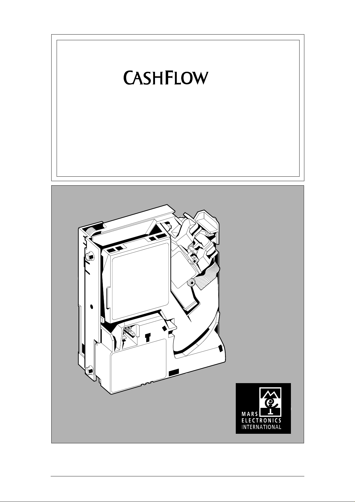
OVERVIEW
The CashFlow330 acceptor is made up of five basic modules,
each of which is available in a number of options:
• Accept Gate
• Discriminator
• Back Cover
• Interface PCB
• Interface PCB Cover
Interface PCB
Cover
Discriminator
Accept Gate
Interface PCB
Back Cover
The acceptor is compact at only 4" and can be used as a stand
alone or, if fitted with the appropriate accessories, can be adapted
for use as a standard 5" front or top entry unit.
MEI have also designed a range of front plates and channels all of
which, when combined with a CashFlow
for most applications.
The acceptors are provided, as standard, with a serial interface
which is known as the HI
available which, when fitted to an acceptor, provide compatibility
with earlier products. These interfaces simply plug into the
discriminator.
Although a number of variants of acceptor are available the basic
operational principles are the same. The following pages describe
the way in which the product works, under the headings of
Mechanical, Electrical, and Operational.
2
interface. Optional interfaces are
©, Mars, Inc., 1994. 3
330 acceptor, are suitable
Page 10
CashFlow 330 acceptor Applications Design Guide
PRODUCT VARIANTS
TOP ENTRY
For top entry applications the acceptor can be mounted in a 4"
moulded channel, a 5" metal channel or an industry standard
channel, forming part of the host machine. The channel applications
require the use of an adaptor.
In addition to this a motorised reject unit can be mounted onto the
4" channel so as to enhance the coin entry and reject functions,
particularly where these are not adjacent to the fixture point in the
host machine. For connection details see the appendix.
4” Moulded Channel
4” Channel with
Remote Reject Unit
5” Channel Adaptor Mounting
4 ©, Mars, Inc., 1994.
Page 11
CashFlow 330 acceptor Applications Design Guide
FRONT ENTRY
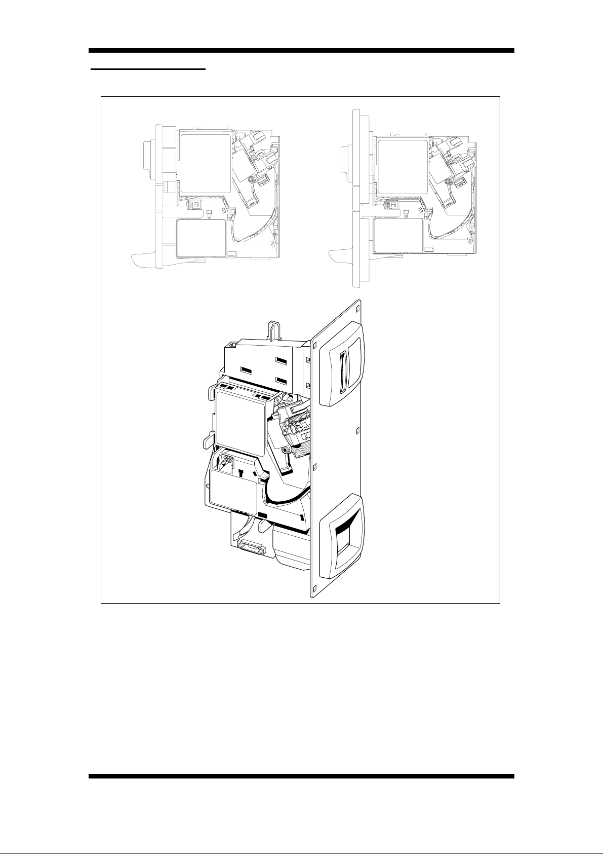
Midi Front Plate
Mini Front Plate
Maxi Front Plate
For front entry applications MEI have designed three new front
plates for use with CashFlow 330 acceptors, these are called the
Mini, Midi, and Maxi front plates.
For detailed information on use of these please refer to the Front
Plate Applications Guide, Mars part number 143512044, or contact
your MEI distributor, who is listed at the end of this book.
©, Mars, Inc., 1994. 5
Page 12
CashFlow 330 acceptor Applications Design Guide
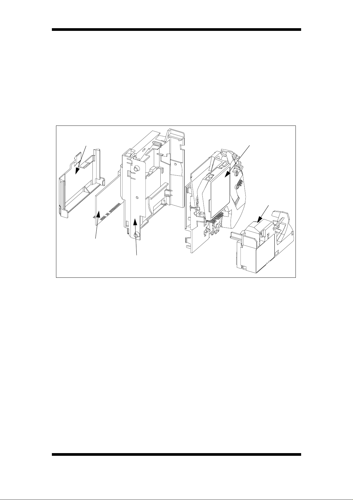
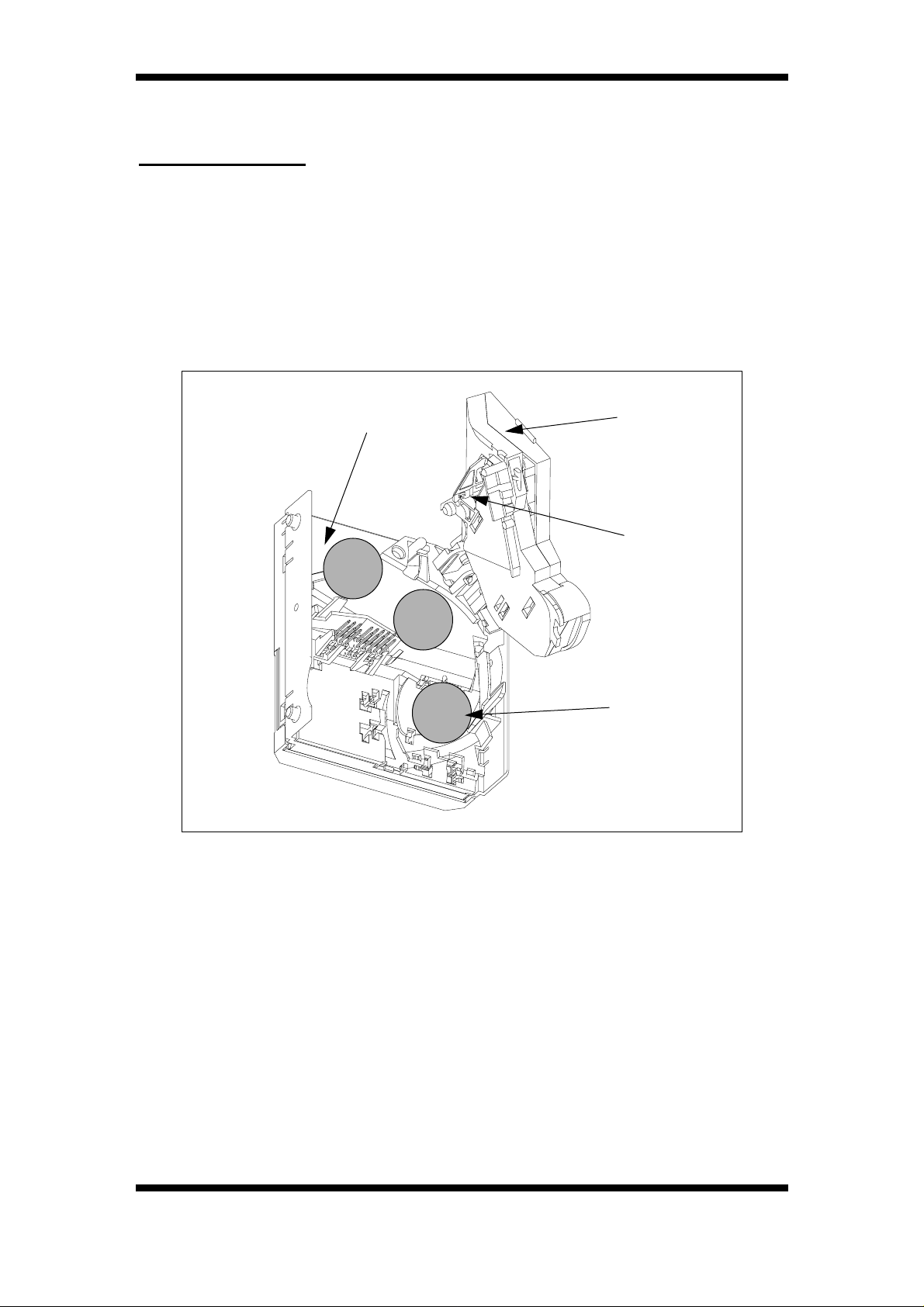
PRODUCT OPERATION
MECHANICAL
The discriminator comprises a flight deck and lid which together
form the coin control and flight path. On the inside of the flight deck
lid there is a mechanical device incorporated near the coin entry
point. This device is known as the coin deflector and brings coins
under control by either removing or dampens their inherent kinetic
energy. It also acts as a cotton catcher.
Flight Deck
Flight Deck
Lid
Coin Deflector
Coin Path
There is a hinge at the top right hand side of the flight deck which
allows coupling of the lid via an intermediate component, known as
the flight deck lid arm. This allows the lid to locate accurately to the
flight deck independently of the hinge. The lid also maintains a
parallel coin throat by being spaced from the deck on three bosses
which locate the lid to the deck.
The design of the lid arm hinge area allows the lid to open to 180
deg. relative to the deck. The opening is restricted to just over 100
deg. by the back cover to prevent the lid fouling other parts such as
front plates etc.
The action of the hinge spring allows the lid to remain open when
past about 100 deg. and will snap shut when closed to about 60 deg.
6 ©, Mars, Inc., 1994.
Page 13
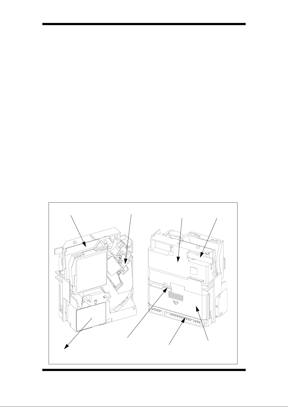
CashFlow 330 acceptor Applications Design Guide
although the lid will need to be pressed to ensure that it is correctly
seated against the deck.
Clearance of any debris or jammed coins from the acceptor is
carried out by opening the lid. This is done by pressing the reject
lever which is located behind the coin entry.
The reject lever assembly forms part of the back cover assembly
and there are versions available for front and top entry mounted
acceptors. They both clip on to the discrimination module.
For front plate mounted acceptors the reject lever assembly is
located on the back of the back cover.
For channel mounted acceptors the reject lever assembly is located
on the top of the back cover.
The lid opening is articulated so as to remain essentially parallel to
the flight deck as the gap between them is increased. This means
that the acceptor can be defined within a smaller total volume
envelope while offering the best coin jam clearance. This means
that the edge of the lid furthest from the hinge does not have to open
more to give greater clearance at the hinge end.
The discriminator also provides the mounting for the PCB.
Coin Entry
Hinge Arm
Back
Cover
Reject
Lever
Accept
Gate
Host Interface
2
HI
©, Mars, Inc., 1994. 7
Customer Interface
Interface
PCB Cover
(0ptional)
Page 14
CashFlow 330 acceptor Applications Design Guide
ELECTRICAL
The CashFlow330 acceptor products are based on a 12V serial
interface. The electrical circuitry is contained in a PCB which is
mounted on the rear of the flight deck behind the back cover.
All internal connections to this PCB are via flexible loom which is
soldered directly to the PCB. This connects to the sensors on the
flight deck, lid, accept gate solenoid and optical coin strobes. Any
external connections to the discrimination PCB are via 0.1” staked
pins accessible through apertures in the back cover. Additional
staked pins on the discrimination PCB are provided to allow optional
interface PCB’s to be fitted.
The base acceptors provide an asynchronous serial interface to the
host machine and CashFlow
product can be provided by fitting one of the optional interface
PCB’s which are plugged directly onto the discrimination PCB. The
base acceptor operates from a 12V supply but can also be
configured for 24V operation by using the correct interface PCB
option.
terminal products. A parallel interface
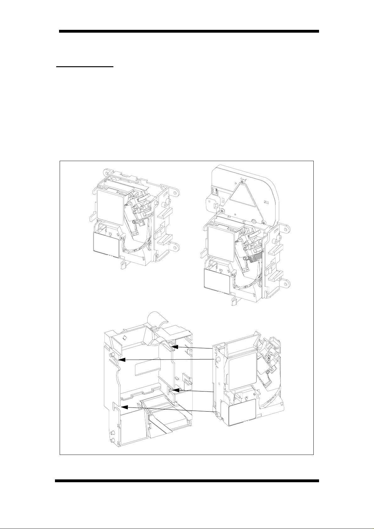
Coins that are correctly discriminated are routed to the accept exit
by energising the accept gate. Coins that are rejected are routed to
the reject exit. Accepted coins generate a coin output signal if they
pass correctly through the coin strobes in the accept gate module.
The accept exit can be either on the right or left as viewed from the
front of the acceptor.
Reject
Coins
Front
Accept RejectReject
Coins Coins
Left Right
Accept
Coins
Right Left Right
Accept
Coins Coins
Coin Exit Options
8 ©, Mars, Inc., 1994.
Page 15

CashFlow 330 acceptor Applications Design Guide
The accept gate module contains a solenoid operated gate, optical
coin strobes and coin routing components. There are three variants
available and the module clips and plugs onto the flight deck.The
coin exits for both accepted and rejected coins are defined by the
type of accept gate fitted.
The electronics on the discrimination PCB operate from 5V
generated by an on-board regulator from the 12V customer supply.If
an optional interface PCB is fitted then the 12V supply comes from
this PCB.
OPERATIONAL
There are some functions of the acceptor which are common across
the whole CashFlow product range. These include coin
discrimination, control and communication.
When a coin is put through the acceptor it’s validity is determined by
measuring certain parameters. It also looks at the coin type status
to define whether the payment is a valid coin or token, or an invalid
coin. Finally, the inhibit status is checked. If the coin is not inhibited,
then it will be accepted and the accept gate opened. Acceptors fitted
with customer interfaces will now activate the coin output lines.
If a coin or token is rejected the accept gate will not open and any
further coins will be inhibited for a period of 500ms. If the following
coin is also rejected then this time period will be restarted.
If the reject lever is operated an Escrow Return (ER) message will
be generated and, if a 0V common interface is fitted, the ER output
will be activated.
©, Mars, Inc., 1994. 9
Page 16
CashFlow 330 acceptor Applications Design Guide
ELECTRICAL INTERFACES
HOST INTELLIGENT INTERFACE (HI2)
The HI2 interface offers serial control of the following functions:
• Inhibiting Coins
• Enabling Coins
2
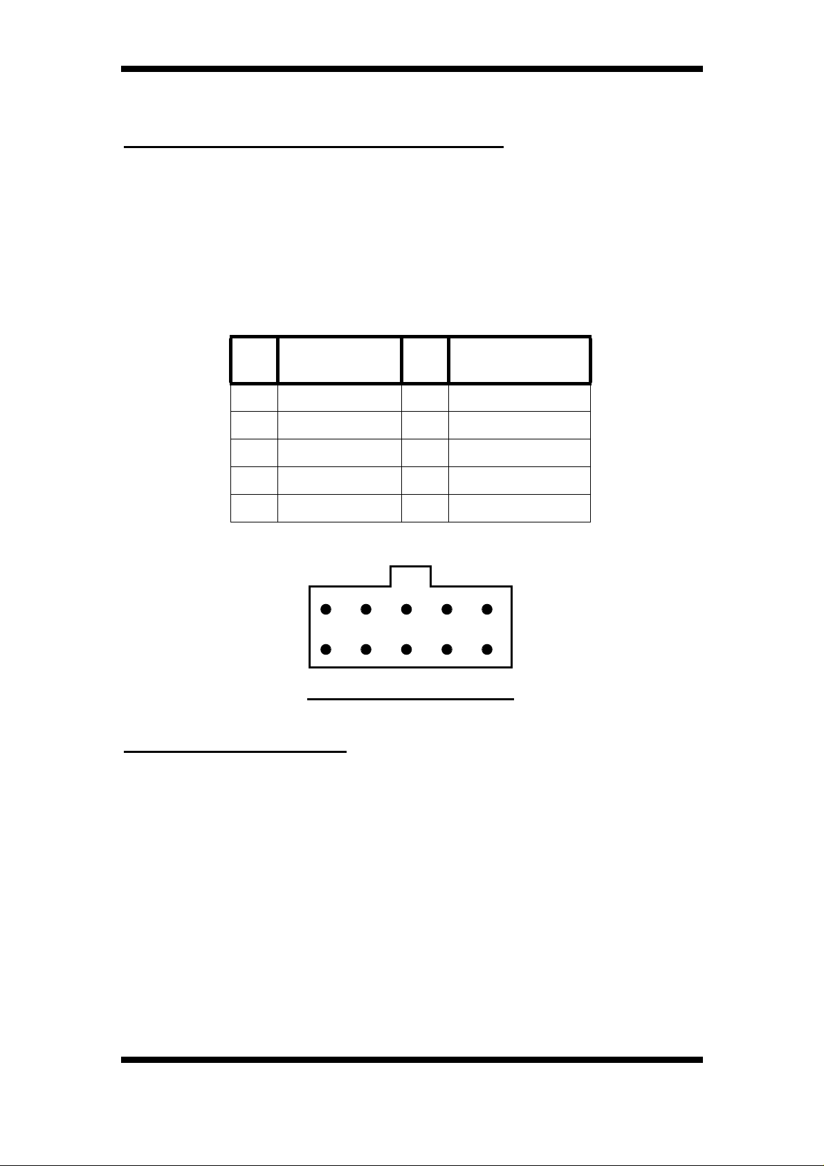
The connections to the 10 way connector of the HI
below.
are shown
PIN
1DATA2 GND
3 BUSY 4 GND
5 RESET 6 POWER FAIL
7 VIN 8 VNEG
9 RESERVED 10 VSOL
Electrical Specifications
SIGNAL
NAME
9
10
Viewed from loom end
PIN SIGNAL NAME
3
5
7
4
6
8
1
2
I/O Ports
Data and Busy
Input high voltage Vih 8.0V min. VIN + 1.5V
max
Input low voltage Vil GND - 1.5V min 1.3V max.
Input impedance Rp 4.7KΩ nom. to VIN
Output high voltage Voh 9.0Vmin. VIN max.
Output low voltage Vol GND min. 0.5V max.
Output sink current Iol ------- 25mA max.
10 ©, Mars, Inc., 1994.
Page 17
CashFlow 330 acceptor Applications Design Guide
VIN
Rx
To internal
logic
Tx
0V
Data and Busy line equivalent circuit
+5V
1n
47K
47K
Rp
DATA or BUSY
GND
The Data and Busy lines are active low signals and are designed to
be wire-ORed with other HI
system load of 3 units.
2
nodes. The selector represents an HI
2
Reset
Input high voltage Vih Open circuit or > 3.5V (5.5V
max.)
Input low voltage Vil (GND - 0.5V) min. 0.9Vmax.
Input impedance Rp 47kΩ nom. to + 5V
Input capacitance Cin 1.5µF nom.
Input series resist. Rserl 56Ω nom.
In addition to the on-board power-on reset circuit, an external device
may reset the system by pulling RESET low. The RESET line is
active low and is intended to be driven by an open collector
transistor referenced to 0V. A series resistor is provided to limit the
peak current drawn when the on-board reset capacitor is discharged
by an external device.
©, Mars, Inc., 1994. 11
Page 18

CashFlow 330 acceptor Applications Design Guide
PF (Power Fail)
Input high voltage Vih 3.7V min. 5.5V max.
Input low voltage Vil (GND - 0.5V) min. 0.9Vmax.
Input impedance Rp 4.7kΩ nom. to + 5V
In addition to the on-board power fail circuit, there is an input on the
host connector to allow an external device to warn of an impending
power failure. The power fail input is active low and is intended to be
driven by an open collector transistor referenced to 0V.
VIN (Power)
Input supply voltage Vin 10V min. 15V max.
(Abs.max. not operational 20V)
Supply voltage ripple Vrip Within Vin min. to max. up to
100Hz
250mV pk-pk frequencies >
100Hz
Supply rise time Trise 75ms max.
Input current Iin 500mA max.
VIN is the input supply voltage referenced to the supply return,
VNEG.
VNEG is connected to GND on the acceptor.
12 ©, Mars, Inc., 1994.
Page 19
CashFlow 330 acceptor Applications Design Guide
APPLICATIONS SUPPORT
The Host Intelligent Interface (HI2) is a high functionality interface for
point to point or multi node systems.
It is currently only available under licence and confidentiality
agreements.
2
Applications support for HI
support. These are all intended to make it straightforward to designin the interface.
HI2 Applications Support
is in the form of documentation and
Documentation Library
Software
Implementors
Guide
‘C’
6805 8051
Protocol
Support
Tools
Protocol
Monitor
©, Mars, Inc., 1994. 13
Page 20

CashFlow 330 acceptor Applications Design Guide
SUPPORT TOOLS
2
With the use of a HI
“Protocol Monitor” software application it is possible to connect a PC
serial port to the HI
interface adaptor and with the aid of the special
2
signals.
HI2 Interface
Adaptor
The adaptor should be plugged into the PC serial port and wired to
the HI
Connector
2
bus as shown below.
10 Way
Product
10
1
2
3
4
5
6
7
8
9
PF
Reserved
Protocol
Monitor
Reset Switch
(if required)
VIN
➜
➜
1
2
3
10 Way HI
4
Adaptor
5
Connector
6
7
8
9
10
+12V (Standard products)
0V
2
14 ©, Mars, Inc., 1994.
Page 21

CashFlow 330 acceptor Applications Design Guide
MACHINE INTERFACE PCB’s
All CashFlow®coin products incorporate a serial machine interface
called HI2 which offers maximum communication flexibility and
security.
Machine interface PCB’s are used to provide compatibility to
industry standard interfaces. There are five different types available,
these are:
• Standard version 112, (0V Common 12V)
• Standard version 124, (0V Common 24V)
• Standard version 212 (0V Common 12V)
• Standard version 312 (0V Common 12V)
• Dual Polarity (12V)
Please note: Not all interfaces are available for all product
configurations. Please contact your Mars Electronics International
representative for guidance.
The interface PCB’s are attached directly to the discrimination PCB
and are enclosed within the back cover of the acceptor.
All of the PCB’s contain a four-bit DIL switch known as the Man
Machine Interface (MMI). This switch can be used to configure
certain aspects of the product.
COMPATIBILITY
Standard versions 112 and 124 are compatible with the following:
MS130, MS135, MS130B1, MS135B1, MS180 and MS185.
Standard version 212 is compatible with:
NRI G13.
Standard version 312 is compatible with:
Azkoyen L60.
Dual Polarity version is compatible with:
MS111, MS111B1, MS115, ME111.
©, Mars, Inc., 1994. 15
Page 22

CashFlow 330 acceptor Applications Design Guide
STANDARD VERSIONS 112 and 124, (0V COMMON 12V & 24V)
These PCB’s provide for 6 coin output lines and 6 individual inhibit
inputs, an all-inhibit input, a flight deck open (ER) output and four
route inhibit inputs.
Standard version 112 (0V Common 12V) interface PCB
Standard version 124 (0V Common 24V) interface PCB
PCB Connectors - versions 112 and 124
The coin outputs are defined as outputs OPA to OPF, and the inhibit
inputs are defined as inputs INHA to INHF. The all-inhibit input is
defined as input ALLINHB, with the flight deck open output being
ER. The route inhibits are defined as inputs INHR1 to INHR4.
The 6 coin outputs consist of open collector transistors referenced
to 0V. The appropriate output becomes active for between 80ms to
120ms to indicate that a particular coin has been accepted.
The 6 individual coin inhibit inputs consist of CMOS inputs with input
protection and pull-down resistors. The inputs are active high to
inhibit coins and if left open circuit will default to accepting coins.
The all-inhibit input consists of a CMOS input with input protection
and pull-up resistor. The input is active low to inhibit coins and if left
open circuit will default to accepting coins.
The flight deck open output consists of an open collector transistor
referenced to 0V. The output is active low to indicate that the flight
16 ©, Mars, Inc., 1994.
Page 23

CashFlow 330 acceptor Applications Design Guide
deck is open and will remain active for a maximum of 500ms.
Pin 1
1
Route Inhibit
Connector
Connector locations - versions 112 and 124
The four route inhibit inputs consist of CMOS inputs with input
protection and pull-up resistors. The inputs are active low to inhibit
a route and if left open circuit will default to route enabled. A shorting
link is required between pins 1 and 2 of the shorting link connector
to enable this mode of operation.
Conn.
Pin
Back Cover
Pin 1
Shorting Link
Connector
Signal Name Signal Name
Pin 1
Interface
Connector
Conn.
Pin
1 INHC INHE 2
3 INHD INHF 4
5 ER ALLINHB 6
7 OPC GND 8
9 OPF OPD 10
11 OPE OPB 12
13 OPA INHB 14
15 INHA VSUPPLY 16
Interface connector - versions 112 and 124
Conn.
Pin
3 RESERVED IF 2
Signal Name Signal Name
INHF L
I
N
K
Conn.
Pin
1
Shorting Link Connector - version 112 and 124
©, Mars, Inc., 1994. 17
Page 24

CashFlow 330 acceptor Applications Design Guide
Route Inhibit Connector - versions 112 and 124
Electrical Interfaces - versions 112 and 124
Power
For 12V operation, VSUPPLY (pin 16) referenced to GND (pin 8):
Conn.
Pin
1 GND
2 POLARISED
3 INHR4
4 INHR3
5 INHR2
6 INHR1
Signal Name
(Loom To Have
Blanked Receptacle)
Input supply voltage Vin 10V min. 15V max.
(Abs.max. not operational 20V)
Supply voltage ripple Vrip Within Vin min. to max. up to
100Hz
250mV pk-pk frequencies
>100Hz
Supply rise time Trise 75ms max.
Input current Iin 500mA max. Acceptor only
Outputs
Off State voltage Voff +30V max.
Leakage current Lin 5µA
On state voltage Vcesat 0.5V max.
On state current Ic 30mA max.
18 ©, Mars, Inc., 1994.
Page 25

CashFlow 330 acceptor Applications Design Guide
Inputs (INHA - INHF)
Individual coin inhibit inputs - (INHA-INHF) Pins 1,2,3,4,14 and 15
Inhibit coins Vin > + 4V (+30V max)
Accept coins Vin between 0V and +1V or input
open circuit
Input impedance 47kΩ nom. to 0V
+5V
INHIBIT
To internal
logic
47K
INPUTS
CMOS
INPUT
All-Inhibit Input: (ALLINHB) Pin 6
Accept coins Vin > + 4V (+ 30V max.) or input
Inhibit coins Vin between 0V and + 1V
Input impedance 47kΩ nom. to + 5V
Route Inhibit inputs: (INHR 1-4) Pins 3, 4,5,6
Route enabled Vin > + 4V (30V max.)
Route inhibited Vin Between 0V and +1V
INHA-F Input Equivalent Circuit
open circuit
or input open circuit
47K
0V
Input impedance: 47kΩ nom. to + 5V
+5V
+5V
47K
To internal
logic
CMOS
INPUT
All-inhibit and Route inhibit input equivalent circuit
©, Mars, Inc., 1994. 19
47K
INHIBIT
INPUT
Page 26

CashFlow 330 acceptor Applications Design Guide
STANDARD VERSIONS 212 and 312, (0V COMMON 12V)
This PCB provides two quite separate interfaces. Version 212 has 6
coin output lines, an all-inhibit input and a flight deck open (ER)
output. This interface operates from a +12V supply.
Version 312 has 4 coin outputs, an alarm output or inhibit input and
an all-inhibit input. This interface operates from a +12V supply.
Provision has also been made for two route inhibit inputs.
Versions 212 and 312 (0V Common 12V) Interface PCB
PCB Connectors - version Standard 212
The six coin outputs consist of open collector transistors referenced
to 0V. The appropriate output becomes active for between 80ms to
120ms to indicate that a particular coin has been accepted.
The coin outputs are defined as outputs OPA to OPF.
Connector locations - Version 212
Connector
Pin
Pin 10
Signal Name Signal Name
Pin 1
Connector
Pin
1 GND VSUPPLY 2
3 OPE OPF 4
5 ER ALLINH 6
7 OPA OPB 8
9 OPC OPD 10
20 ©, Mars, Inc., 1994.
Page 27

CashFlow 330 acceptor Applications Design Guide
The all-inhibit input consists of a CMOS input with input protection
and pull-down resistor. The input is active high to inhibit coins and if
left open circuit will default to accepting coins. The all-inhibit input is
defined as input ALLINH
The flight deck open output consists of an open collector transistor
referenced to 0V. The output is active low to indicate that the flight
deck is open and will remain active for a maximum period of 500ms.
The flight deck open output is defined as output ER.
PCB Connectors - version Standard 312
The four coin outputs consist of open collector transistors
referenced to 0V. The appropriate output becomes active for
between 80ms to 120ms to indicate that a particular coin has been
accepted. The coin outputs are defined as outputs OPA to OPD.
The alarm output consist of an open collector transistor referenced
to 0V. The output becomes active, if enabled, when the acceptor
detects a fraud condition. The alarm output is defined as output
ALARM /INH.
Pin 10
Connector locations - Version 312
Connector
Pin
Signal
Name
The same interface pin is also used for an inhibit input which
consists of a CMOS input with input protection and pull-up resistor.
The input is active high to inhibit coins and if left open circuit will
default to inhibiting coins. The input may be configured via the
acceptor inhibit map, to inhibit some or all of the coins in the coin set.
1 2345678910
OP A
GND
VSUPPL Y
OPB
Pin 1
OPC
OPD
ALLINH
INHR1
INHR2
ALARM/INH
©, Mars, Inc., 1994. 21
Page 28

CashFlow 330 acceptor Applications Design Guide
The inhibit input is defined as input ALARM/INH. The all-inhibit input
consists of a CMOS input with input protection and pull-up resistor.
The input is active high to inhibit coins and if left open circuit will
default to inhibiting coins. The input may be configured via the
acceptor inhibit map, to inhibit some or all of the coins in the coin set.
The all-inhibit input is defined as input ALLINH.
Electrical Interfaces
Power
Standard 2 interface; VSUPPLY (pin 2) referenced to GND (pin1):
Standard 3 interface; VSUPPLY (pin 1) referenced to GND (pin2):
Input supply voltage Vin 10V min. 15V max.
(Abs. max. not operational 20V)
Supply voltage ripple Vrip Within Vin min. to max. up to
100Hz
250mV pk-pk frequencies >
100Hz
Supply rise time Trise 75ms max.
Input current. Iin 500mA max. Acceptor only
Outputs
All outputs:
Off state voltage Voff +30V max.
Leakage current Iin 5µA
On state voltage Vcesat 0.5V max.
On state current Ic 30mA max.
Standard 2; All-inhibit input (ALLINH)
Inhibit coins Vin > +4 V (+30V max)
Accept coins Vin between 0V and +1V
or input open circuit
Input Impedance: 47kΩ nom. to 0V
22 ©, Mars, Inc., 1994.
Page 29

CashFlow 330 acceptor Applications Design Guide
+5V
To internal
logic
CMOS
INPUT
Standard 212 ALLINH input equivalent circuit
Standard 3; Inhibit inputs (ALLINH, ALARM/INH and INHR1-7)
Accept coins Vin > +4 V (+30V max)
or input open circuit
Inhibit coins Vin between 0V and +1V
Input Impedance: 47kΩ nom. to +5V
47K
ALL INHIBIT
INPUT
47K
0V
+5V
+5V
47K
To internal
logic
CMOS
INPUT
Standard 312 - Inhibit inputs equivalent circuit
47K
INHIBIT
INPUTS
©, Mars, Inc., 1994. 23
Page 30

CashFlow 330 acceptor Applications Design Guide
DUAL POLARITY
This interface operates from a nominal 12V supply and self
configures to either positive or negative common operation. In either
mode of operation this interface offers 6 coin output lines, an output
common, 6 individual inhibit inputs and power connections.
Dual Polarity Interface PCB
Coin outputs - positive common
For positive common operation the OPCOM line must be positive
with respect to GND and the coin output lines should be connected
through a load to a voltage more negative than the OPCOM line.
Coin outputs - negative common
For negative common operation the OPCOM line must be negative
with respect to GND or connected to GND. The coin output lines
should be connected through a load to a voltage more positive than
the OPCOM line.
With either of these options it is possible to operate in a pulsed
mode by allowing the OPCOM line to float until it is polled by the
host machine.
When a coin is accepted one of the coin output lines becomes
active.
24 ©, Mars, Inc., 1994.
Page 31

CashFlow 330 acceptor Applications Design Guide
PCB Connector - Dual Polarity
The coin outputs are defined as OPA to OPF, and the inhibit inputs
as INHA-INHF.
Conn.
Pin
1OPA
2 OPB
3 OPCOM
4 OPF
5 POLARISING
6 OPE
7 OPD
8 POLARISING
9 OPC
10 INHC
11 VSUP
12 GND
Signal Name
13 INHD
14 INHE
15 INHF
16 INHB
17 INHA
Electrical Specifications
Power
VSUP (pin 11) referenced to GND (pin 12):
Input supply voltage Vin 10V min. 15V max.
(Abs. max. not operational 20V)
Supply voltage ripple Vrip Within Vin min. to max. up to 100Hz
250mV pk-pk frequencies > 100Hz
Supply rise time Trise 75ms max.
Input current Iin 1440mA max.
©, Mars, Inc., 1994. 25
Page 32

CashFlow 330 acceptor Applications Design Guide
Inputs
Individual coin inhibit inputs:
Inhibit coins Vin > + 4V (+20Vmax) or input open
circuit
Accept coins Vin between 0V and + 1V
Input impedance 12kΩ nom. to + 5V
+5V
+5V
12K
To internal
logic
CMOS
INPUT
0V
Inhibit input equivalent circuit
Outputs - Positive Common
OPCOM (pin3) referenced to GND (pin12):
Input voltage Vin 5V min 26V max.
(4.5V min 5V max.
Ic max =10mA)
All outputs:
47K
INHIBIT
INPUT
Off state voltage Voff (OPCOM - 27V) min.
Leakage current Iin 5µA
On state voltage Vcesat (OPCOM - 1.5V) min.
On state current Ic 40mA max.
26 ©, Mars, Inc., 1994.
Page 33

CashFlow 330 acceptor Applications Design Guide
Outputs -Negative Common
OPCOM (pin3) referenced to GND (pin12):
Input voltage Vin -22V min. 0V max.
(0V min. 0.5V max. Ic
max=10mA)
All outputs:
Off state voltage Voff (OPCOM + 27V) min.
Leakage current Iin 5µA
On state voltage Vcesat (OPCOM + 1.5V) min.
On state current Ic 40mA max
+5V
To internal
logic
0V
Coin output equivalent circuit
1N4148
Coin
Output
1N4148
Output
Common
©, Mars, Inc., 1994. 27
Page 34

CashFlow 330 acceptor Applications Design Guide
CONFIGURATION
FACTORY CONFIGURATION
The CashFlow 330 acceptor is configured for:
• Serial interface
and / or
• Parallel interface
The accept gate modules are factory configured for specific product
types. It is therefore essential that if you need to change the accept
gate you change like for like.
Specific Coinsets
The acceptor is pre-programmed to accept a specific range of coins
and/or tokens from the following countries.
This list does not preclude any other coinsets not specifically listed.
Australia Hungary Singapore
Austria India South Africa
Bahrain Israel South Korea
Belgium Italy Spain
Canada Japan Sweden
Colombia Kuwait Switzerland
Cyprus Malta Taiwan
Denmark Mexico Turkey
Eire Netherlands UAE
Finland New Zealand UK
France Norway USA
Germany Portugal
Greece Saudi Arabia
28 ©, Mars, Inc., 1994
Page 35

CashFlow 330 acceptor Applications Design Guide
FIELD CONFIGURATION
The CashFlow® 330 acceptor product offers various field
configuration options. There are two methods available: via an
®
interface PCB (MMI) or by use of a Mars
held terminal.
VIA MAN MACHINE INTERFACE (MMI)
The Man Machine Interface is designed to provide a simple standalone interface which allows frequently used functions to be
accessed and varied by an operator or route person.
The actual interface consists of a 4-bit DIL switch on the machine
interface PCB. The following functions are available:
• Inhibit an individual coin
• Enable an individual coin
Route Alpha 250 hand
4-bit DIL switch
Set to enable a coin
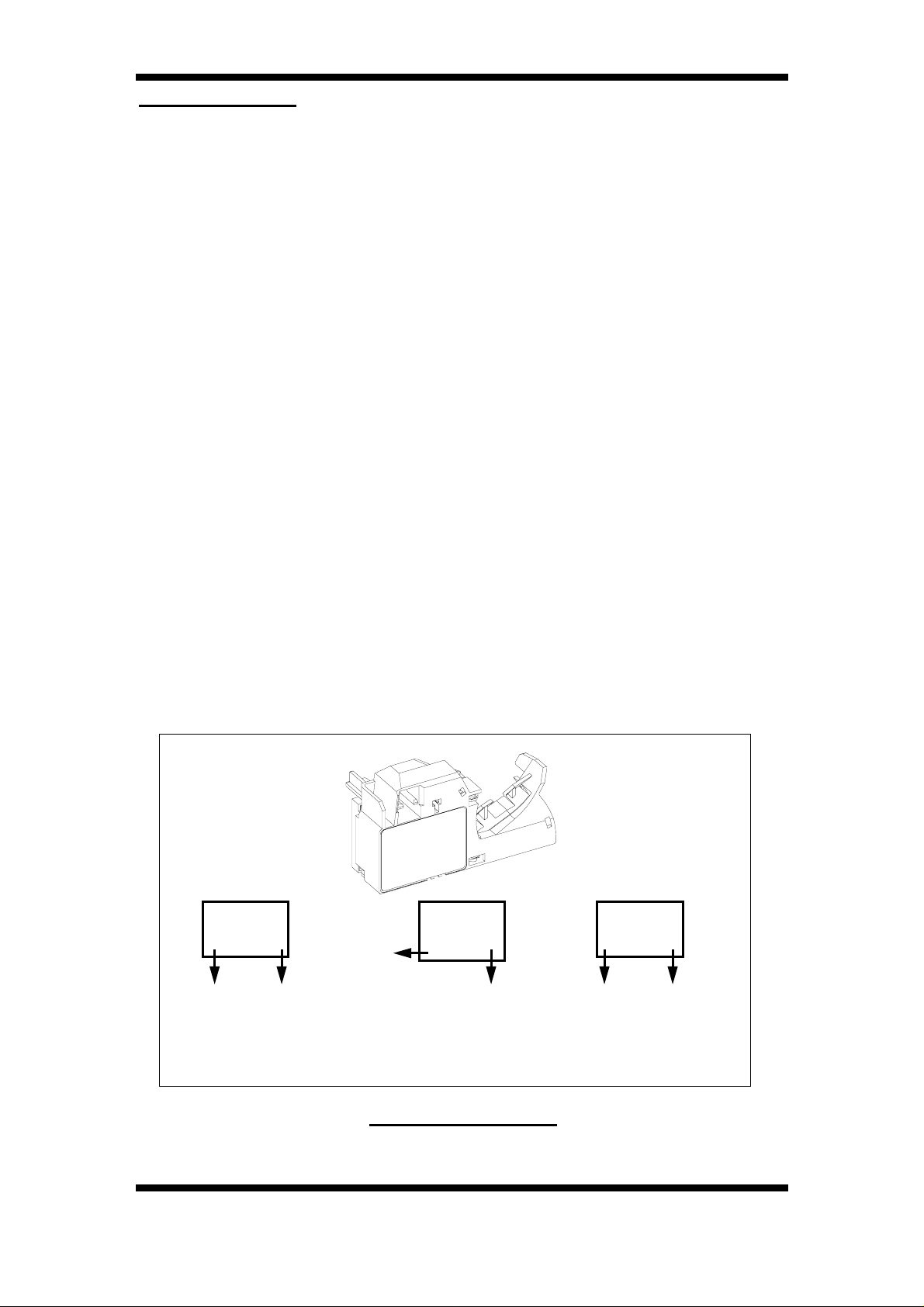
To change the function of the product there is a sequence of events
that must be followed in order:
1 Switch off power and remove the acceptor module from
the machine.
2 Disconnect the loom(s).
3 Remove the interface PCB cover by pressing
downwards in the direction of the arrow on the cover.
4 Re-connect the loom(s).
5 Switch on power to the acceptor module.
Interface PCB
6 Adjust the switch positions on the 4-bit DIL switch.
7 Replace the acceptor module back into machine.
8 Press the reject lever within a 4 minute time-out period.
9 Insert coins until desired function has been achieved.
10 Press the reject lever.
©, Mars, Inc., 1994. 29
Page 36

CashFlow 330 acceptor Applications Design Guide
Important points to remember
• The acceptor module must be powered up before
• The reject lever must be pressed within the 4
Care should be taken while the acceptor is not mounted in the
machine.
To Inhibit a Coin
1 Adjust slide switches to: 1=ON, 2=ON, 3=OFF, 4=ON.
2 Press the reject lever.
3 Insert coins to be inhibited until they are accepted.
4 Press the reject lever to return to operational mode.
changing the switch positions.
minute timeout period to return to the normal
operational mode.
To Enable a Coin
1 Adjust slide switches to: 1=ON, 2=ON, 3=OFF, 4=OFF.
2 Press the reject lever.
3 Insert coins to be enabled until they are accepted.
4 Press the reject lever to return to operational mode.
When you have completed configuring the acceptor module the
interface PCB cover needs to be replaced. To do this follow the
instructions below:
1 Switch off power and remove the acceptor module from
the machine.
2 Disconnect the loom(s). When disconnecting hold down
the interface PCB before pulling on the loom.
3 Replace the interface PCB cover.
4 Re-connect the loom(s).
5 Place the acceptor module back into the machine.
6 Switch on power.
7 Test the unit to ensure it is working correctly.
30 ©, Mars, Inc., 1994
Page 37

CashFlow 330 acceptor Applications Design Guide
VIA MARS ROUTE ALPHA 250 TERMINAL
Mars® Route Alpha Terminal
CashFlow® 330 connections to Terminal
The Mars
certain data held at addresses which affect the way the acceptor
operates. Each address has a unique number which identifies the
feature you wish to read or change.
The following pages will explain how to access and change the data
in certain addresses. At the end of this section there is a list of
addresses and the allowed values.
The terminal is connected via a six way terminal connector at the
front of the acceptor module as shown in the above diagram.
Route Alpha 250 terminal is used to check or change
©, Mars, Inc., 1994. 31
Page 38

CashFlow 330 acceptor Applications Design Guide
Key Functions
ENTER
LEFT
Reset Key: used to reset all modes and to initialise any settings that
you have changed. If the reset key is pressed while an address is
being updated then the address may not be updated. The reset key
must be pressed to activate the changes that you have made.
Up Key: used to increase the value displayed on the screen.
RESET
DISPLAY
UP
RIGHT
DOWN
Down Key: used to decrease the value displayed on the screen.
Left Key: used to scroll the display to the left when a large number
is being accessed that cannot be fully displayed on the screen.
Right Key: used to scroll the display to the right when a large
number is being accessed that cannot be fully displayed on the
screen.
Enter Key: used to change between the address and data displays.
Other Facilities Of The Terminal
The terminal has built-in features to speed up its use, including the
ability to scan at a higher speed with the keys auto repeating, to
automatically roll over from its highest to lowest address and to
inform the operator should a communication error occur.
Auto Repeating Keys
If either the UP or DOWN keys are kept pressed they automatically
repeat. The repeat speed of the key increases the longer the key is
held down.
32 ©, Mars, Inc., 1994.
Page 39

CashFlow 330 acceptor Applications Design Guide
Double Click Hotkeying
If a key is doubled clicked (pressed twice in quick succession) then
this causes the address number to increment by a larger amount.
e.g. if the user starts at address number 1 then double clicks the UP
key, the address will jump to 40, double click again the address will
jump to address 100 etc. You can also double click the DOWN key
to decrement by larger amounts.
Using The Terminal
As soon as the terminal is connected to an acceptor it powers up
and interrogates the product.
The terminal display will clear and briefly show a message that
indicates the version of software in the terminal. A display of [0 1.0]
means software with a version number of 1.0 is fitted in the terminal.
Power up message
After a few seconds the display will show the number [1.] or [1.-]. Not
all configuration items are applicable to every product but all the
address values are shown on the display. If the value for the
address is applicable to the product a dash will be present at the far
right position on the display. The value can then be accessed and
changed if required
.
Software version = 1.0
No dash displayed.
Address is not
accessible for this
product
Dash is displayed.
Address is therefore
accessible
©, Mars, Inc., 1994. 33
Page 40

CashFlow 330 acceptor Applications Design Guide
The basic operation to alter the information held in an address is:
1 Connect the terminal to the CashFlow
2 Wait for the terminal to power up correctly.
3 Select the address by using the UP and DOWN keys.
4 Examine the data by pressing the ENTER key.
5 Alter the data value by pressing the UP or DOWN keys
6 Press the ENTER key to return to displaying addresses.
7 Press the RESET key to initialise the new value.
When the terminal is displaying values stored at addresses, no
decimal point will be displayed.
module.
until the new value has been reached.
acceptor
If an error occurs with the communication between the terminal and
the acceptor the display will show an error message of four half
height zeroes.
Error message
This message will stay on the display. Pressing the ENTER key will
then revert the display to showing the current address. If the error
occurred while updating an address then the value of that address
should be checked as it may not have been updated correctly.
As the screen is capable of only displaying four digits at any one
time the number displayed on the screen can be scrolled if it is
greater than 9999 by using the LEFT and RIGHT keys. The left or
rightmost digit will flash indicating an extra digit can be examined by
use of the scrolling keys e.g. Value is 12345
Press RIGHT key
Press LEFT key
Flashing Flashing
34 ©, Mars, Inc., 1994.
Page 41

CashFlow 330 acceptor Applications Design Guide
The tables below show you how the addresses can be reconfigured
and their possible values.
Address
1 Coin 1 inhibit 0-1 0 = coin allowed,1 = inhibited
2 Coin 2 inhibit 0-1 0 = coin allowed,1 = inhibited
3 Coin 3 inhibit 0-1 0 = coin allowed,1 = inhibited
4 Coin 4 inhibit 0-1 0 = coin allowed,1 = inhibited
5 Coin 5 inhibit 0-1 0 = coin allowed,1 = inhibited
6 Coin 6 inhibit 0-1 0 = coin allowed,1 = inhibited
7 Coin 7 inhibit 0-1 0 = coin allowed,1 = inhibited
8 Coin 8 inhibit 0-1 0 = coin allowed,1 = inhibited
9 Coin 9 inhibit 0-1 0 = coin allowed,1 = inhibited
10 Coin 10 inhibit 0-1 0 = coin allowed,1 = inhibited
11 Coin11 inhibit 0-1 0 = coin allowed,1 = inhibited
12 Coin12 inhibit 0-1 0 = coin allowed,1 = inhibited
Parameter
Range
Meaning
13
14
15 Accept direction 0-1 0 = left,1 = right
16 Strobes 1/2/4/8
21 Coin 1 type 0-2
22 Coin 2 type 0-2
Coin13 inhibit
(Serial acceptor only)
Coin14 inhibit
(Serial acceptor only)
0-1 0 = coin allowed,1 = inhibited
0-1 0 = coin allowed,1 = inhibited
Value = sum of codes
1 = direction strobe left
2 = direction strobe right
4 = post gate left,
8 = post gate right
0 = coin
1 = value token
2 = vend token
0 = coin
1 = value token
2 = vend token
©, Mars, Inc., 1994. 35
Page 42

CashFlow 330 acceptor Applications Design Guide
Address
23 Coin 3 type 0-2
24 Coin 4 type 0-2
25 Coin 5 type 0-2
26 Coin 6 type 0-2
Parameter
Range
0 = coin
1 = value token
2 = vend token
0 = coin
1 = value token
2 = vend token
0 = coin
1 = value token
2 = vend token
0 = coin
1 = value token
2 = vend token
Meaning
27 Coin 7 type 0-2
28 Coin 8 type 0-2
29 Coin 9 type 0-2
30 Coin 10 type 0-2
31 Coin11 type 0-2
32 Coin 12 type 0-2
0 = coin
1 = value token
2 = vend token
0 = coin
1 = value token
2 = vend token
0 = coin
1 = value token
2 = vend token
0 = coin
1 = value token
2 = vend token
0 = coin
1 = value token
2 = vend token
0 = coin
1 = value token
2 = vend token
33
34
36 ©, Mars, Inc., 1994.
Coin 13 type
(Serial acceptor only)
Coin 14 type
(Serial acceptor only)
0-2
0-2
0 = coin
1 = value token
2 = vend token
0 = coin
1 = value token
2 = vend token
Page 43

CashFlow 330 acceptor Applications Design Guide
Address
140,143,
146,149,
152,155,
158,161,
Parameter
Inhibit lines 1 - 8,
inhibits map part i
0 -15
Range
Value = sum of codes where
1/2/4/8 = coins 1/2/3/4
Meaning
141,144,
147,150,
153,156,
159,162.
142,145,
148,151,
154,157,
160,163.
164,166,
168,170,
172,174,
176,178,
180,182,
184,186
165,167,
169,171,
173,175,
177,179,
181,183,
185,187
Inhibit lines 1 - 8,
inhibits map part ii 0 -15
Inhibit lines 1 - 8,
inhibits map part iii 0-15
Coins 1-12 output
map part i
Coins 1-12 output
map part ii 0-15
0-15
Value = sum of codes where
1/2/4/8 = coins 5/6/7/8
Value = sum of codes where
1/2/4/8 = coins 9/10/11/12
Value = sum of codes where
1/2/4/8 = outputs a/b/c/d
Value = sum of codes where
1/2/4/8 = outputs e/f/g/h
188 Inhibit pull up polarity 0-1 0 = pull down 1 = pull up
189 Master inhibit polarity 0-1 0 = active high 1 = active low
190
191 FIB enable 0-1 0 = disabled 1 = enabled
External inhibit
enable
0-1 0 = disabled 1 = enabled
©, Mars, Inc., 1994. 37
Page 44

CashFlow 330 acceptor Applications Design Guide
ENVIRONMENTAL PERFORMANCE
Products will meet the following environmental specification:
TEMPERATURE RANGE
Working ambient 0° to 60°C
Max rate of change 15°C/hr. non condensing
Storage -40° to +75°C
Recovery 1 hour per 10°C to working ambient
temperature range
Solar radiation Max. working ambient applies
HUMIDITY
Operational 10% to 90% RH
Storage 10% to 95% RH
Recovery 1 hour per 10% RH to working ambient
humidity range
% RH
100
75
50
25
-40/95
0/90
0/75
43/90
45/75
43/95
STORAGE
FULL
WORKING
RANGE
OPTIMUM
WORKING
RANGE
0
-40 -20 0 20 40 60 80
Temperature / Humidity specification
38 ©, Mars, Inc., 1994.
60/10
75/10
°C
Page 45

CashFlow 330 acceptor Applications Design Guide
VIBRATION
Operational - units will not be damaged by these conditions:
Vibration
(Coin acceptance will not be seriously affected.)
TRANSPORTATION
Units in the packed state will not sustain any physical damage under
these conditions:
Shock Half sine, 30g shock, 18ms dur. Refer to BS
2011: part 2.1 Ea: 1988 / IEC 68-2-27
Bump 1000 bumps 6ms duration at 25g. Refer to
BS 2011: part 2.1 Eb: 198 7/ IEC 68-2-29
0.25g at 5 to 500 Hz.
Intermittent over the unit’s
life. Refer to BS2011: part
2.1 Fc:1983 / IEC 68-2-6
Free Fall 1000mm fall onto packing faces. Refer to
BS 2011: part 2.I Ed: 1992 / IEC 68-232:1975
Crush Neatly stacked units of the same type may
be stacked to a height of 2 metres.
©, Mars, Inc., 1994. 39
Page 46

CashFlow 330 acceptor Applications Design Guide
LIQUIDS
Water
The units inclusive of PCBs will be splash protected.
The coin entry encourages excess water towards the reject path on
an accept right product, and the front of the product out of the coin
path. Coin stall under these conditions will be minimised.
Salt water
Prolonged exposure in a salt laden atmosphere will lead to PCB
corrosion damage. Suitable packaging will be required when
shipped by sea.
Other Liquids
Exposure to these will cause impairment of function. To include:
dilute carbonic acid, dilute citric acid, carbonated drinks, beer, tea,
coffee, chocolate, soup, syrup and sugar residue, uric acid.
Comments:
• Certain beverages and the dilute acids may cause
similar effects to salt water if they contact the PCB’s.
• Performance when wet will be similar to that described
for water.
• Liquids which leave a residue on drying which affects
the passage of coins will cause malfunction
•
40 ©, Mars, Inc., 1994.
Page 47

CashFlow 330 acceptor Applications Design Guide
SAFETY AND SUBMISSIONS
CLASSIFICATION
The defined product will satisfy the requirements of a class II (unearthed) appliance as defined in IEC 335.
The products will comply with:
• UL 756 “Coin and currency changers and actuators”
• IEC 335, 3rd Edition “Safety of Household and similar
Electrical Appliances”
FLAMMABILITY
All major plastic parts will be moulded in materials with a
flammability rating of UL 94 V-2/IEC 707 FV2 or better. Some small
parts are moulded in materials with a minimum flammability rating of
94 -HB/IEC 707 FH2.
POWER SUPPLY INPUT PROTECTION
Overcurrent protection is not included in the product and should be
provided as part of the host machine.
Recommended fuse ratings are:
• 12V: 2.0A
Other protection methods may be used providing the overall
protection envelope remains within that defined by the fuse
characteristics.
MECHANICAL PARTS
The CashFlow®products will not contain mechanically moving
parts, or sharp edges, which can present a hazard in normal use.
©, Mars, Inc., 1994. 41
Page 48

CashFlow 330 acceptor Applications Design Guide
CASHFLOW MODULES COMPATIBILITY
COIN EXITS
Viewed from rear
RF=Reject Front
AR=Accept Right
RL=Reject Left
RR=Reject Right
AL=Accept Left
Front Entry
Back Cover
DISCRIMINATOR
AR RLAR RF RR AL
Top EntryTop Entry
Back CoverBack Cover
0V Common
I/F 12v
0V Common
I/F 24v
Dual Polarity
I/F 12v
" Channel ✘✔✔
4
" Top
5
Entry
Adaptor
Mini F/P ✔✘✘
Midi F/P ✔✘✘
Maxi F/P ✘✘✔
✔✔✔
✔✔✔
✔✔✔
✘✔✘
42 ©, Mars, Inc., 1994.
Page 49

CashFlow 330 acceptor Applications Design Guide
COMPATIBILITY with EARLIER PRODUCTS
If you are currently using the MS/ME100 product range then the
table below will help you identify the acceptor and accessory
required for compatibility. The typical applications shown are a
guide only to the options available.
NEW NEW NEW
Available
Options
4" Acceptor
Stand Alone
Juke Boxes,
Typical
Application
Replaces
MS111 ✔✔
Replaces
ME111 ✔✔
Replaces
ME115 ✔✔
Replaces
MS130 ✔✔
Cigarette M/c
Channel
Mounted
4" Acceptor
+Top Entry Adaptor
4" Acceptor
+Mini Front Plate
Video Games,
Table Top
Vending
4" Acceptor
+Midi FrontPlate
4" Acceptor
+Maxi Front Plate
Pin
Ball
M/c’s
©, Mars, Inc., 1994 43
Page 50

CashFlow 330 acceptor Applications Design Guide
MARS ELECTRONICS INTERNATIONAL
OFFICES
AUSTRALIA
MARS ELECTRONICS INTERNATIONAL
302 PARRAMATTA ROAD
AUBURN
NEW SOUTH WALES, 2144
TELEPHONE: 2 - 7375390
FACSIMILE: 2 - 7375399
CANADA JAPAN
MARS ELECTRONICS INTERNATIONAL
37, HOLLAND DRIVE
BOLTON
ONTARIO, L7E 5S4
TELEPHONE: 416 - 239 - 2782
FACSIMILE: 416 - 239 - 3322
ITALY
MARS ELECTRONICS INTERNATIONAL
27011 BELGIOIOSO (PV)
VIALE DANTE, 40
TELEPHONE: 0382 - 979313
FACSIMILE: 0382 - 970790
MARS ELECTRONICS INTERNATIONAL
A DIVISION OF MASTER FOODS LTD.
3F MUSASHI-KOSUGI TOWER PLACE
403 KOSUGIMACHI 1-CHOME
NAKAHARA-KU
KAWASAKI-SHI
KANAGAWA-KEN 211
TELEPHONE: 44 - 712 - 1315
FACSIMILE: 44 - 712 - 1439
FRANCE SPAIN
MARS ELECTRONICS INTERNATIONAL
BOULEVARD DES CHANATS
BP 7
45550 ST. DENIS DE L’HOTEL
TELEPHONE: 38 - 59 - 6161
FACSIMILE: 38 - 59 - 6172
GERMANY SWITZERLAND
MARS ELECTRONICS INTERNATIONAL
INDUSTRIERING 17 A
41751 VIERSEN
TELEPHONE: 02162 - 9560
FACSIMILE: 02162 - 41544
GREAT BRITAIN UNITED STATES
MARS ELECTRONICS INTERNATIONAL
ESKDALE ROAD
WINNERSH TRIANGLE
WOKINGHAM
BERKSHIRE, RG41 5AQ
TELEPHONE: 01734 - 697700
FACSIMILE: 01734 - 446412
MARS ELECTRONICS INTERNATIONAL
M.a DE MOLINA, 40-3
28006 MADRID
TELEPHONE: 9 - 3379182
FACSIMILE: 91- 5635517
MARS ELECTRONICS INTERNATIONAL
CH. PONT-DU-CENTENAIRE 109
PLAN-LES-OUATES
P.O. BOX 2650
1211 GENEVA 2
TELEPHONE: 22 - 8840505
FACSIMILE: 22 - 8840504
MARS ELECTRONICS INTERNATIONAL
1301 WILSON DRIVE
WEST CHESTER
PA 19380
TELEPHONE: 610 - 4302500
FACSIMILE: 610 - 4302694
a
44 ©, Mars, Inc., 1994.
Page 51

CashFlow 330 acceptor Applications Design Guide
INDEX
A
Accept Exit 8
Accept Gate Module 2, 3, 9
Acceptor Module 2, 29, 30
Applications Support 13
B
Back Cover 2, 3
C
Channel Mount Adaptor 2
Channel Mounting 2
Classification 41
Coin Deflector 6
Coin Entry 2
Coin Outputs - Negative Common 24
Coin Outputs - Positive Common 24
Coin Routing 9
Coin Type Status 9
Compatibility 15, 42, 43
Configuration 28, 29
D
Discrimination PCB 15
Discriminator Module 2, 3, 6
Disposal Of Product 1
Dual Polarity Interface 2
E
Electrical Interfaces 10
Electrical Operation 8
Electrical Specification 10, 12, 18, 19, 22,
23, 25, 26, 27
Electro Magnetic Compatibility 40
Enable Teach 29, 30
Enable Teach Mode 10
Environmental Immunities 40
Environmental Performance 1, 38, 39, 40
Escrow Return 9
©, Mars, Inc., 1994. 45
Page 52

CashFlow 330 acceptor Applications Design Guide
F
Flammability 41
Flight Deck 6
Flight Deck Lid 6
Flight Deck Lid Arm 6
Front Plate Definition 2
G
Glossary 2
H
Hinge Spring 6
Host Intelligent Interface 10, 13, 14
Humidity 38
I
Inhibit Status 9
Inhibit Teach 29, 30
Inhibit Teach Mode 10
Interface Definition 2
Interface PCB 3, 29, 30
L
Liquids 40
Local Expansion Interface 13
M
Machine Interface PCB 15, 16, 17, 20, 24,
29
Man Machine Interface (MMI) 15, 29, 30
MARS ELECTRONICS INTERNATIONAL 44
Mars® Route Alpha 250 Terminal 29, 31
Mechanical Operation 6
Mechanical Parts 41
O
Operating Voltages 1
Operational Function 9
Optical Coin Strobes 9
P
Parallel Interface 8, 28
PCB Connector 16, 17, 20, 21, 25,
26
PCB Cover 3, 30
Power Down 29
46 ©, Mars, Inc., 1994
Page 53

CashFlow 330 acceptor Applications Design Guide
Power Supply Input Protection 41
Power Up 29, 30
Product Operation 6
Product Overview 3
R
Reject Lever 30
Route Inhibit Connector 18
S
Safety 1, 30
SELV 2
Serial Interface 3, 8, 15, 28
Shorting Link Connector 17, 18
Specific Coinsets 28
Submissions and Safety 41
Support Tools 14
T
Temperature Range 38
Terminal Addresses 35
Terminal Key Functions 32, 33, 34
Test 30
Time-Out 29
Transportation 39
V
Vibration 39
Numerics
0V Common Interface 2
©, Mars, Inc., 1994. 47
Page 54

CashFlow 330 acceptor Applications Design Guide
APPENDIX
INTERFACE DRAWINGS
The following mechanical interface drawings are included in this
section.
Drawing
Number
4" ACCEPTOR 000491002
5" TOP ENTRY ADAPTOR 148895001
MINI FRONT PLATE 149278001
MIDI FRONT PLATE 149281001
MAXI FRONT PLATE 149265001
4" CHANNEL 149498001
REMOTE REJECT UNIT 001347001
48 ©, Mars, Inc., 1994.
Page 55

CashFlow 330 acceptor Applications Design Guide
©, Mars, Inc., 1994 49
Page 56

CashFlow 330 acceptor Applications Design Guide
50 ©, Mars, Inc., 1994.
Page 57

CashFlow 330 acceptor Applications Design Guide
©, Mars, Inc., 1994 51
Page 58

CashFlow 330 acceptor Applications Design Guide
52 ©, Mars, Inc., 1994.
Page 59

CashFlow 330 acceptor Applications Design Guide
©, Mars, Inc., 1994 53
Page 60

CashFlow 330 acceptor Applications Design Guide
54 ©, Mars, Inc., 1994.
Page 61

CashFlow 330 acceptor Applications Design Guide
©, Mars, Inc., 1994 55
Page 62

REPRESENTATIVE:
REPRESENTATIVE:
UNITED STATES
UNITED STATES
1301 Wilson Drive
1301 Wilson Drive
West Chester
West Chester
Pa 19380
Pa 19380
Telephone: 610- 4302500
Telephone: 610- 4302500
Facsimile: 610- 4302694
Facsimile: 610- 4302694
GREAT BRITAIN
GREAT BRITAIN
Eskdale Road
Eskdale Road
Winnersh Triangle
®
®
™
™
Winnersh Triangle
Wokingham
Wokingham
Berkshire, RG41 5AQ
Berkshire, RG41 5AQ
Telephone: 01734- 697700
Telephone: 01734- 697700
Facsimile: 01734- 692668
Facsimile: 01734- 446412
SWITZERLAND
SWITZERLAND
Ch. Pont-du-Centenaire 109
Ch. Pont-du-Centenaire 109
Plan-les-Ouates
Plan-les-Ouates
P.O. Box 2650
P.O. Box 2650
1211 Geneva 2
1211 Geneva 2
Telephone: 22- 8840505
Telephone: 22- 8840505
Facsimile: 22- 8840504
Facsimile: 22- 8840504
FRANCE
FRANCE
15 Rue De La Malmaison
Boulevard Des Chenats
95500 Gonesse
BP 7
Telephone: 1- 34531180
45550 St. Denis de L’hotel
Facsimile: 1- 34531700
Telephone: 38 - 59 - 6534
Facsimile: 38 - 59 - 6172
GERMANY
GERMANY
Industriering 17 A
Industriering 17 A
41751 Viersen
41751 Viersen
Telephone: 02162- 9560
Telephone: 02162- 9560
Facsimile: 02162- 41544
Facsimile: 02162- 41544
ITALY
ITALY
27011 Belgioioso (Pv)
27011 Belgioioso (Pv)
Viale Dante, 40
Viale Dante, 40
Telephone: 0382- 979313
Telephone: 0382- 979313
Facsimile: 0382- 970790
Facsimile: 0382- 970790
SPAIN
SPAIN
M.a De Molina, 40-3
28006 Madrid
M.a De Molina, 40-3
28006 Madrid
Telephone: 91- 3379182
Telephone: 91- 3379182
Facsimile: 91- 5635517
Facsimile: 91- 5635517
AUSTRALIA
AUSTRALIA
302 Parramatta Road
302 Parramatta Road
Auburn
Auburn
New South Wales, 2144
New South Wales, 2144
Telephone: 02- 737- 5390
Telephone: 02- 737- 5390
Facsimile: 02- 737- 5399
Facsimile: 02- 737- 5399
JAPAN
JAPAN
Mars Electronics International
Mars Electronics International
3f Masushi-kosugi Tower Place
3f Masushi-kosugi Tower Place
403 Kosugimachi 1-chome
403 Kosugimachi 1-chome
Nakahara-ku
Nakahara-ku
Kawasaki-shi
Kawasaki-shi
Kanagawa-ken 211
Kanagawa-ken 211
Telephone: 44 - 712 - 1315
Telephone: 44 - 712 - 1315
Facsimile: 44 - 712 - 1439
Facsimile: 44 - 712 - 1439
CANADA
CANADA
Mars Electronics International
Mars Electronics International
57, King Georges Road
37, Holland Drive
Toronto
Bolton
Ontario, M8X Il6
Ontario, L7E 5S4
Telephone: 416 239 2782
Telephone: 416 239 2782
Facsimile: 416 239 3322
Facsimile: 416 239 3322
a
a
 Loading...