

TOSHIBA Bi-CMOS Integrated
Circuit Silicon Monolithic
TB62713N/FTB62713N/F
TB62713N/F
TB62713N/FTB62713N/F
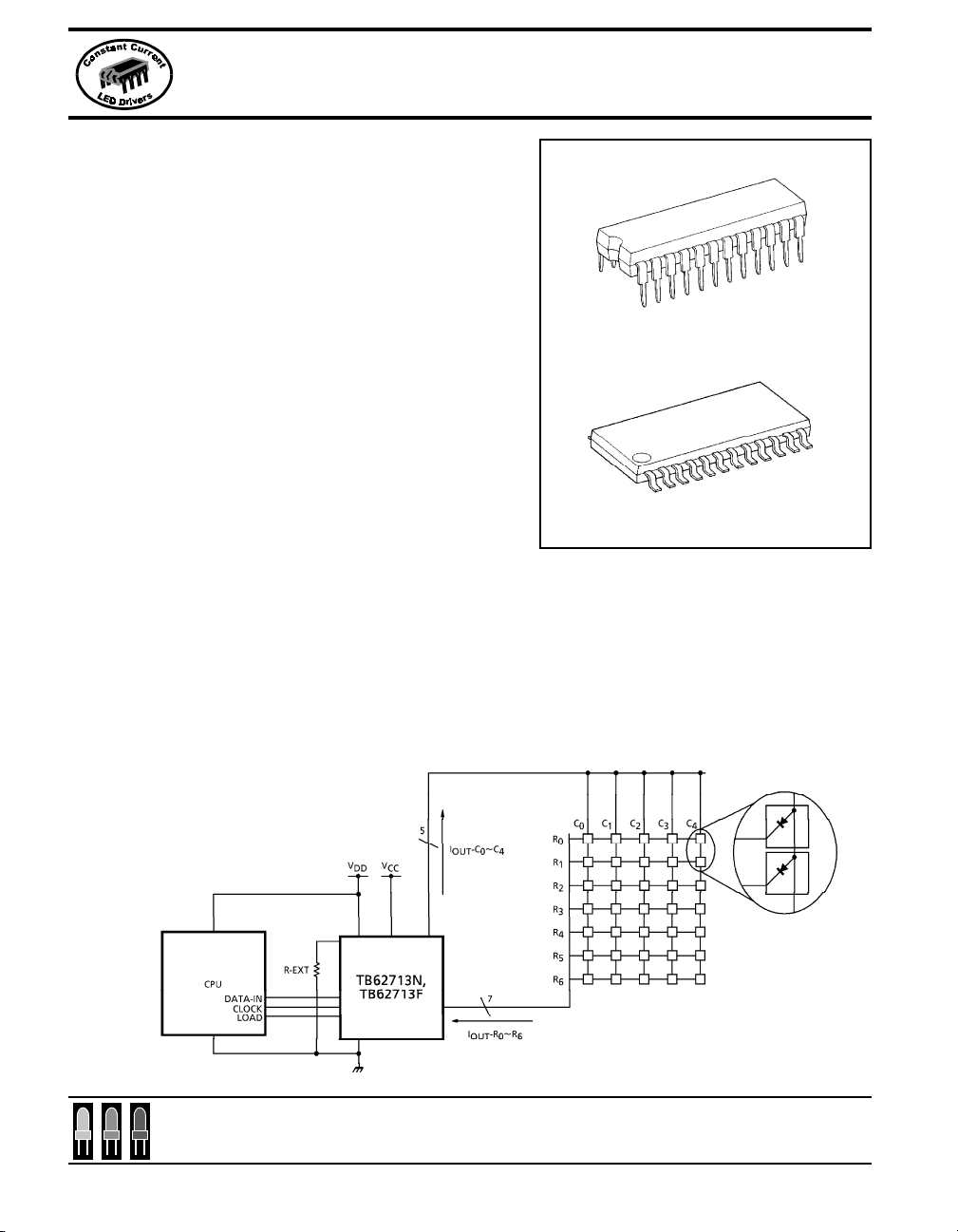
Intelligent 5 X 7 LED Dot Matrix Display Controller
Featuring Toshiba’s exclusive Constant Current
technology.
The TB62713F is an intelligent, Constant Current, 5 X
7 LED dot matrix display decoder and driver. The stand
alone device includes all of the decode, multiplex and
driver circuitry necessary to control a 5 X 7 LED matrix.
An internal character set includes 128 characters to
simplify programming and refresh functions are
handled automatically. All display data, including a 16
step brightness control is input via the serial data port.
Features
• Constant Current row drivers for consistent display
brightness.
• Single device saves labor and board space.
• 128 character internal character set simplifies design efforts.
• Automatically handles multiplex and display refresh tasks.
• 16 step programmable brightness control.
• Available in thru hole and surface mount packages.
• Data out cascade connection port.
TB62713N
SDIP24-P-300-1.78 Weight: 1.62g (Typ.)
TB62713F
SSOP24-P-300-1.00 Weight: 0.32g (Typ.)
Performance Characteristics
VDD = 4.5V~5.5V
Column source output: -17V / 350mA
Row select output: 17V / 0-50mA
Max transition frequency: 15MHz
marktech
optoelectronics
For up-to-date product info visit our web site at www.marktechopto.com All specifications subject to change.
608
Toll Free: (800) 98-4LEDS
120 Broadway • Menands, New York 12204
• Fax: (518) 432-7454
TOSHIBA Bi-CMOS Integrated
Circuit Silicon Monolithic
TB62713N/FTB62713N/F
TB62713N/F
TB62713N/FTB62713N/F
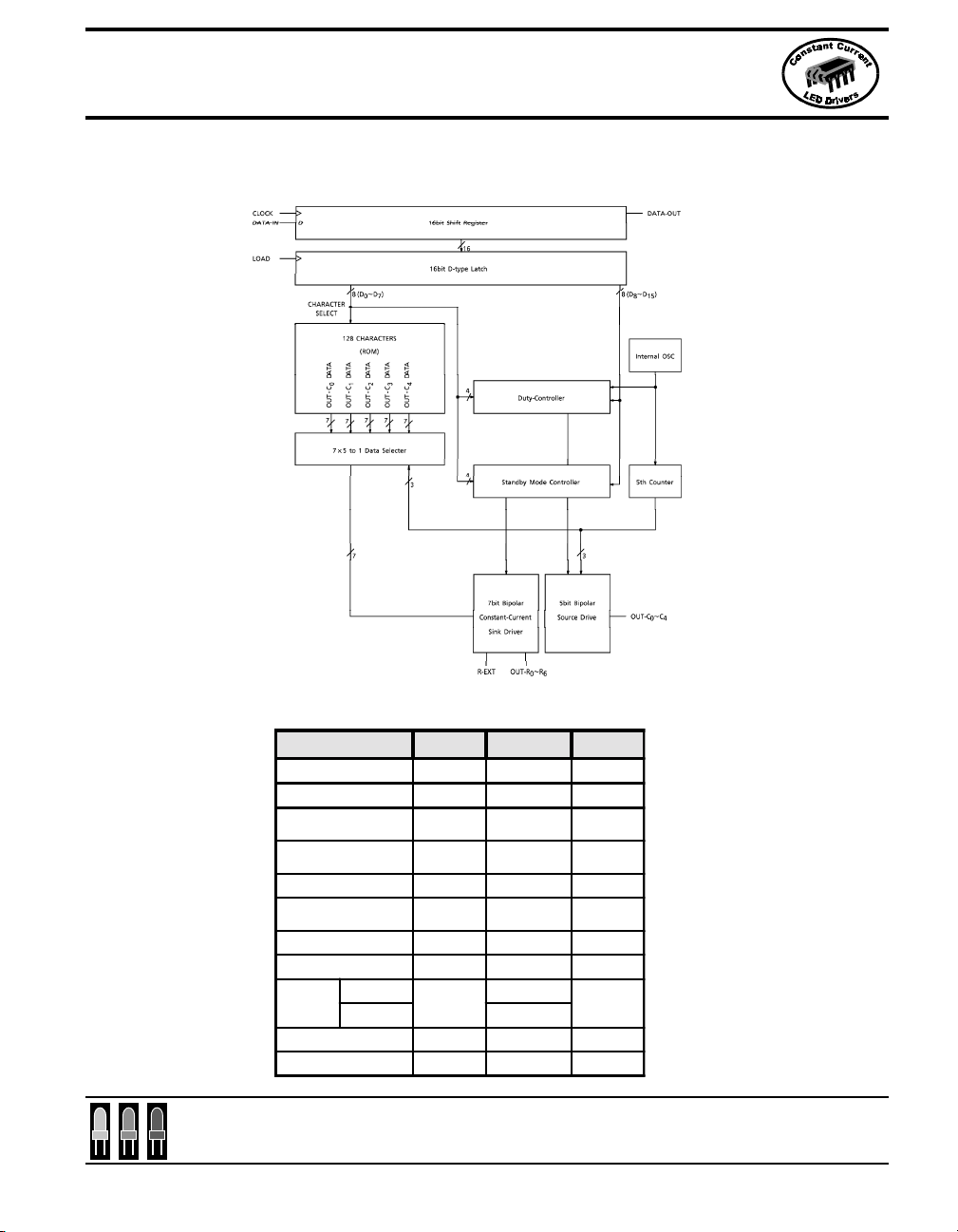
Block Diagram
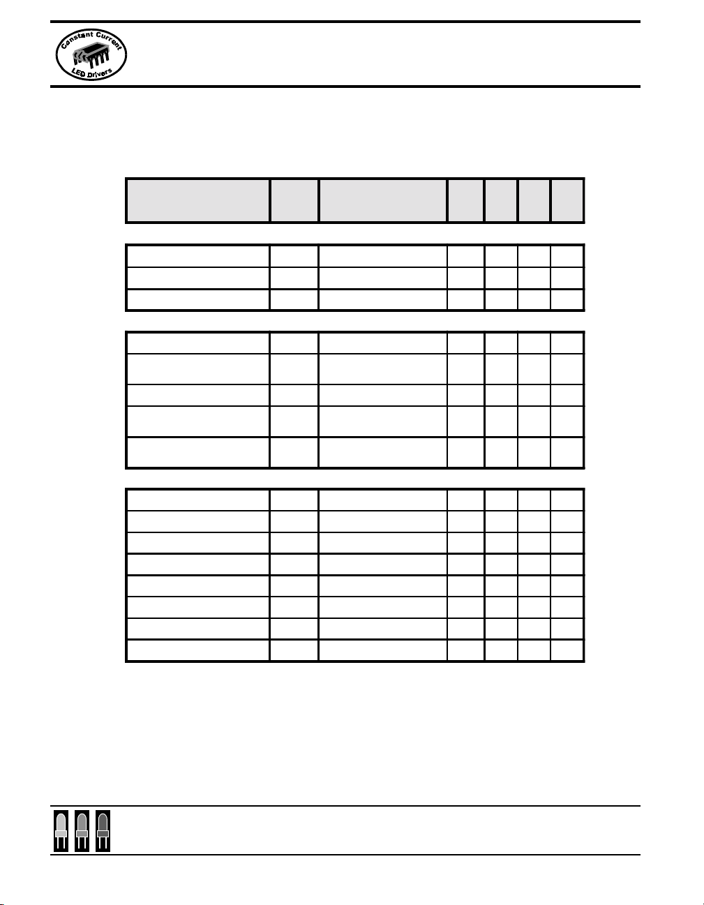
Maximum Ratings:
CHAR ACTERIS TICS SYMBOL RATING UNIT
Supply Voltag e VDD 7.0 volts
LED Supply Voltag e VCC 17.0 volts
Sour ce Output Curre nt
Columns 0~4
Row Drive Current
Rows 0~6
Output Curre nt IOH/IOL +/-5 .0 mA
Inpu t Vo ltag e VIN
Clo ck Fre quency FC LK 15 .0 MHz
Tota l Output Current IVDD 4 20.0 mA
Power
Dissipation
Operation Temperature Topr -40 ~ +85 °C
Storage Temperature Tstg -55 ~+150 °C
TB62713N
TB62713F 0.62
marktech
optoelectronics
For up-to-date product info visit our web site at www.marktechopto.com All specifications subject to change.
ICO -420.0 mA
IRO 60 .0 mA
-0.3 ~ VD D
~+0.3
Pd
1.78
volt s
120 Broadway • Menands, New York 12204
Toll Free: (800) 98-4LEDS
W
• Fax: (518) 432-7454
609
TOSHIBA Bi-CMOS Integrated
Circuit Silicon Monolithic
TB62713N/FTB62713N/F
TB62713N/F
TB62713N/FTB62713N/F
Recommended Operating Condition:
CH ARACTERIS TICS SYMBOL
Output S tage
IC C1 1
Supply Current
IC C2 1
Column C0~C4 Scanning
Frequency
Col. C0~C4 Leakage Current ILEAK1 4 All off mode, VCC=17V — — -20 µA
Row R0~R6 Leakage Current ILEAK2 4 All off mode, VCE=17V — — 20 mA
Row R0~R6 Si nk C urrent IRO 3
Col. C0~C4 Leakage Voltage VOUT 5
Logic
Supply Current
Operating Supply Current IDD3 6
High Level Input Current IIH — D ata-in, Load&Clock VIN=5V — — 1 µA
Low Level Output Current IIL — Data-in, Load&Clock VIN=0V — — -1 µA
High Level Output Voltage
Low Level Output Voltage
Clock Frequency FCLK 6 Cascade connected 10 — — MHz
fOSC 2
IDD1 6 Standby Mode, Ta=25°C — — 200 µA
IDD2 6 Blank Mode, Ta=25°C — — 12.5 mA
VOH1 6 Data out, IOH=-1mA 4.6 — — V
VOH2 6 Data-out, IOH=-1µA — VDD — V
VOL1 6 Data out, IOL=-1mA — — 0.4 V
VOL2 6 Data-out, IOL=-1µA — 0.1 — V
TEST
CIRCUIT
CONDITION MIN. TYP. MAX. UNIT
Set normal operation mode
Rext=590Ω, Out R0~R6, all
on VCC = 5V, Ta=25°C
Set normal operation mode
Rext=590Ω, Out R0~R6, all
on VCC = 12V, Ta=25°C
Normal operation mode
VDD=4.5 - 5.5V
Normal operation, VCE=.7V,
Rext=590Ω,
Normal operation mode
IOUT-cn = -350mA
Normal operating mode
fCLK=10MHz, Ta=25°C
Da ta-in:Ro ws R0~ R6 on
— 370 — mA
— 390 — mA
300 600 1200 Hz
36.5 43 49.4 µA
3.0 — — V
— — 20.5 mA
marktech
optoelectronics
For up-to-date product info visit our web site at www.marktechopto.com All specifications subject to change.
Toll Free: (800) 98-4LEDS
120 Broadway • Menands, New York 12204
• Fax: (518) 432-7454
610
TOSHIBA Bi-CMOS Integrated
Circuit Silicon Monolithic
TB62713N/FTB62713N/F
TB62713N/F
TB62713N/FTB62713N/F
Switching Characteristics:
CHARACTERISTICS SYMBOL CONDITION MIN . TYP. MAX. UNIT
Data Hold Time (D-IN Clock) tDHO — 10 — ns
Data Set-up Time (D-IN Clock) tDST — 20 — ns
Serial Output Delay tPDSO CL=10pf — 25 — ns
High Level Pulse Width Of Clock tCLKH — 30 — ns
Low Level Pulse Width Of Clock tCLKL — 30 — ns
Pulse Width Of Load tw LD — 100 — ns
Setup Time (Clock-Load) tCLK-LD — 50 — ns
Setup Time (Load-Clock) tLD-CLK — 50 — ns
Col. C0~C6 Propagation Delay
(Load-Outn)
Col. C0~C6 Rise Time (OUTn) tr CO CL=10pf 0.2 1.0 — µs
Col. C0~C6 Fall Time (OUTn) tf CO CL=10pf 0.2 1.0 — µs
Row R0 ~ R4 Pro pag ation Delay
(Load-Rn)
Row R0~R4 Ris e Time (Rn) tr RO CL=1 0pf 0.4 2.0 — µs
Row R0~R4 Fall Time (Rn) tf RO CL=10pf 0.4 2.0 — µs
tPDCO CL=10pf — — 5.0 µs
tPDRO CL=10pf — — 10.0 µs
marktech
optoelectronics
For up-to-date product info visit our web site at www.marktechopto.com All specifications subject to change.
Toll Free: (800) 98-4LEDS
120 Broadway • Menands, New York 12204
• Fax: (518) 432-7454
611
TOSHIBA Bi-CMOS Integrated
Circuit Silicon Monolithic
TB62713N/FTB62713N/F
TB62713N/F
TB62713N/FTB62713N/F
Recommended Operating Conditions:
CHARACTERIS TICS SYMBOL CONDITION MIN. TYP. MAX. UNIT
Outpu t Stag e
Supply Voltage VCC 4.0 — 15.0 V
Column C0~C6 Output Current ICO VCE=0.7V — — 50 mA
Row R0~R4 Output Current IRO VOUT=3.0V — — -280 mA
Logic
Supply Voltage VDD 4.5 — 5.5 V
High Level Input Current IIH
Low Level Input Current IIL Data-In, Load&Clock,VIN=0V — — -1 µA
High Level Input Voltage VIH
Low Level Input Voltage VIL — —
Switching Condition
Data Hold Time (D -IN Clock) tDHO 30 — — ns
Data Setup Time (D-IN Clock) tDST 50 — — ns
Propagation Delay (Clock D-Out) tPDS O CL=10pf 50 — — ns
High Level Pulse Width Of Clock tCLKH 30 — — ns
Low Level Pulse Width Of Clock tCLKL 30 — — ns
Pulse Width Of Load twLD 150 — — ns
Setup Time (Clock-Load) tCLKLD 100 — — ns
Setup Time (Load-Clock) tLDCLK 100 — — ns
Data-In,
Load&Clock,VIN=VDD
—— 1µA
0.7
—— V
VDD
0.3
V
VDD
marktech
optoelectronics
For up-to-date product info visit our web site at www.marktechopto.com All specifications subject to change.
612
Toll Free: (800) 98-4LEDS
120 Broadway • Menands, New York 12204
• Fax: (518) 432-7454
TOSHIBA Bi-CMOS Integrated
Circuit Silicon Monolithic
TB62713N/FTB62713N/F
TB62713N/F
TB62713N/FTB62713N/F
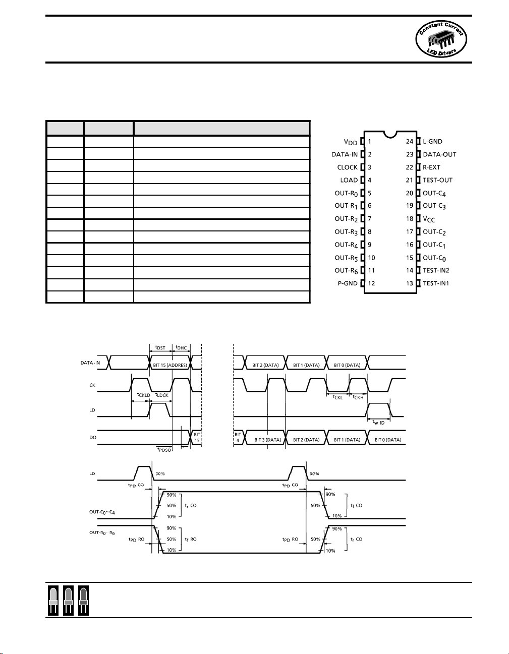
Terminal Description:
PIN No. NAME FUNCTION
1VDDLogic Supply Voltage
2 Data IN Serial Data Input To Shift Register
3 Clock (CLK) Clock Input Terminal
4 Load (LD) Load Input Terminal
5-11 Row R0 ~R6 Output Terminal to Row Ca thodes
12 P-GND GND fo r Row Out
13 Test In 2 Test Terminal - Grounded During Normal Operation
14 Te st In 1 Te st Terminal - Grounded During Normal Operation
5-17,19,2 Column C0-C4 Output Terminal to Column Anodes
18 V
21 Test OUT During Normal Operation Leave open
22 Rext C onstant C urre nt Pro gra mming Termi nal
23 Data Out (DO) Cascade Connection To Next Display Stage
24 L-GND Logic & Analog Ground Terminal
CC
Supply Voltage For LED s
Timing Diagram:
marktech
optoelectronics
For up-to-date product info visit our web site at www.marktechopto.com All specifications subject to change.
Toll Free: (800) 98-4LEDS
120 Broadway • Menands, New York 12204
• Fax: (518) 432-7454
613

TOSHIBA Bi-CMOS Integrated
Circuit Silicon Monolithic
TB62713N/FTB62713N/F
TB62713N/F
TB62713N/FTB62713N/F
Data Input
Data is input on the SERIAL-IN terminal. Each 16 bit serial word includes an address (D8 - D15)
and data (D0 - D7). A low to high transition load command on the LOAD terminal loads the data
into the appropriate registers following the 16th clock pulse.
Operation
Serial data is input on the DATA-IN terminal beginning with the most significant bit (MSB). Data
is clocked through the 16 bit shift register on the rising edge of the clock. A Low to High transition on the LOAD input following the 16th (LSB) bit latches the 16 bit word into the 16 bit D-type
latch.
Each 16 bit word typically includes 8 address bits and 8 data bits. The first four data bits,
beginning with D15 (MSB) ~ D12 select the Action mode (see figure 1). These global commands determine the overall function the device is to perform and includes Blank, Normal
Operation, Load Register, All On and Stand-by. Data bits D11~D8 select the particular register to
be loaded (see figure 2) should the load register function be selected. Data bits D7~D0 (LSB)
define the specific commands required to program the display and define the brightness setting
(duty cycle).
Figure 1. Action Mode
REGISTER DATA
FUNCTION
Blank
(Rows & Co lumns All Off)
Normal Operation 0 0 0 1 — — — 1 - - - H
Load Register
(Duty, Character Data)
All On (Col. C0~C4 All On) 0 0 1 1 — — — 3 - - - H
Stand-By 0 1 0 0 — — X 4 - - - H
D15 D14 D13 D12 D11~D8 D7~D4 D3~D0 Hex Code
0 0 0 0 — — — 0 - - - H
0 0 1 X X X X 2 xxx H
INIT IAL
STATE
⇐
“x” indicates that data is required in this field to execute the function. “-” indicates that data in
this field is not required and not recognized.
marktech
optoelectronics
For up-to-date product info visit our web site at www.marktechopto.com All specifications subject to change.
614
Toll Free: (800) 98-4LEDS
120 Broadway • Menands, New York 12204
• Fax: (518) 432-7454
TOSHIBA Bi-CMOS Integrated
Circuit Silicon Monolithic
TB62713N/FTB62713N/F
TB62713N/F
TB62713N/FTB62713N/F
Action Mode
1. Blank - Constant current segment drivers are off resulting in an all segments off condition.
Data D15 ~ D12 are 0. D11~D0 are not relevant in blank mode. (Note: the device draws <
12.5ma in Blank mode.)
2. Normal (Operation) - Instructs device to display data loaded during previous steps. D11~ D0
are not relevant in the Normal Operation mode.
3. Load Register - Directs the device to recognize and load D11~ D0. In this mode D11 ~ D8
determines the specific register to be loaded (see figure 2) and D7 ~ D0 serves as the actual
data to be loaded for programming the brightness (duty cycle) or the particular digit.
4. All On - All constant current row drivers are on resulting in an all dots illuminated condition.
D11 ~ D0 are not relevant in this mode.
5. Stand By - All display drivers off condition. The Stand-By command turns off all internal bias
currents and serves as a low power consumption mode (<.2ma). Used with Stand-By set up
commands “All Data Clear” or “Data Not Cleared” (table 7).
The initial state, upon power up, is the BLANK state.
Application Note:
Stand-By and Blank perform similar functions in that the display is totally blank when either
command is input. Stand-By provides a low power consumption (<.2ma current draw on VDD)
mode by turning off all internal bias currents in the internal driver circuits. The Stand-By command also cuts off the Rext bias current used to regulate the programmed constant current
within the device.
marktech
optoelectronics
For up-to-date product info visit our web site at www.marktechopto.com All specifications subject to change.
Toll Free: (800) 98-4LEDS
120 Broadway • Menands, New York 12204
• Fax: (518) 432-7454
615

TOSHIBA Bi-CMOS Integrated
Circuit Silicon Monolithic
TB62713N/FTB62713N/F
TB62713N/F
TB62713N/FTB62713N/F
LOAD REGISTER Mode
Figure 2. LOAD REGISTER Mode
REGISTER DATA
FUNCTION
Load Duty Register 2H 0 0 0 0 X X 20XXH
Load Character Data Register 2H 0 0 0 1 X X 21XXH
“x” indicates that data is required in this field to execute the function. “-” indicates that data in
this field is not required and not recognized.
Selects the specific register to be loaded. The LOAD REGISTER mode is enabled by the Load
Register Action mode command (see Figure 1 - Action mode).
1. Duty Register - Enables the device to accept duty cycle (brightness) setting. (see table 3 Duty Cycle control register). Sixteen brightness steps (0/16 to 15/16) are available.
2. Character Data Register - Enables the device to accept the data to program the 5 X 7 matrix
character as encoded in D7~D0.
D15~D12 D11 D10 D9 D8 D7~D4 D3~D0 Hex Code
marktech
optoelectronics
For up-to-date product info visit our web site at www.marktechopto.com All specifications subject to change.
616
Toll Free: (800) 98-4LEDS
120 Broadway • Menands, New York 12204
• Fax: (518) 432-7454
TOSHIBA Bi-CMOS Integrated
Circuit Silicon Monolithic
TB62713N/FTB62713N/F
TB62713N/F
TB62713N/FTB62713N/F
Brightness Control
Brightness is controlled by controlling the “on time” duty cycle. The device allows for 16 brightness as illustrated in list 3 with 0/16 as the dimmest setting (not illuminated) to 15/16 as the
brightest setting. The duty cycle control register is addressed with a 20 Hex command at
D15~D8 and the appropriate data per list 3 at D3~D0. D7~D4 are not recognized by the duty
cycle register. The initial state, upon power up is 15/16, or full brightness.
REGISTER DATA
DUTY CYCLE
0/16 20H — 0 0 0 0 20X 0H
1/16 20H — 0 0 0 1 20X1H
2/16 20H — 0 0 1 0 20X 2H
3/16 20H — 0 0 1 1 20X 3H
4/16 20H — 0 1 0 0 20X4H
5/16 20H — 0 1 0 1 20X5H
6/16 20H — 0 1 1 0 20X6H
7/16 20H — 0 1 1 1 20X7H
8/16 20H — 1 0 0 0 20X 8H
9/16 20H — 1 0 0 1 20X 9H
10/16 20H — 1 0 1 0 20XAH
11/16 20H — 1 0 1 1 20XBH
12/16 20H — 1 1 0 0 20XCH
13/16 20H — 1 1 0 1 20XDH
14/16 20H — 1110 20XEH
15/16 20H — 1 1 1 1 20XFH
D15~D8 D 7~D4 D3 D2 D1 D0 Hex Code
INITIAL
STATE
⇐
“x” indicates that data is required in this field to execute the function. “-” indicates that data in
this field is not required and not recognized.
marktech
optoelectronics
For up-to-date product info visit our web site at www.marktechopto.com All specifications subject to change.
Toll Free: (800) 98-4LEDS
120 Broadway • Menands, New York 12204
• Fax: (518) 432-7454
617

TOSHIBA Bi-CMOS Integrated
Circuit Silicon Monolithic
TB62713N/FTB62713N/F
TB62713N/F
TB62713N/FTB62713N/F
STAND-BY Commands
Two STAND-BY commands are available as illustrated in Table 7. STAND-BY / NO DATA
CLEAR places the device in a power save mode (see application note - ACTION Mode section)
while leaving data intact in the various registers. This mode is enabled by a 4 Hex command at
D15~D12 and 0 Hex at D3~D0. D11~D4 are not relevant in the STAND-BY / NO DATA CLEAR
Mode.
STAND-BY / DATA CLEAR also places the device in a power save mode and clears data in the
various registers leaving registers in their initial state. This mode is enabled by a 4 Hex command at D15~D12 and 1 Hex at D3~D0. D11~D4 are not relevant in the STAND-BY / NO DATA
CLEAR Mode.
REGISTER DATA
D15~D8 D7~D4 D3 D2 D1 D0 Hex Code
Stand-By (No Data Clear) 4-H — 0 0 0 0 4XX0H
Stand-By (Clear Data) 4-H — 0 0 0 1 4XX1H
“ x” indicates that data is required in this field to execute the function. “-” indicates that data in
this field is not required and not recognized.
marktech
optoelectronics
For up-to-date product info visit our web site at www.marktechopto.com All specifications subject to change.
618
Toll Free: (800) 98-4LEDS
120 Broadway • Menands, New York 12204
• Fax: (518) 432-7454
TOSHIBA Bi-CMOS Integrated
Circuit Silicon Monolithic
TB62713N/FTB62713N/F
TB62713N/F
TB62713N/FTB62713N/F
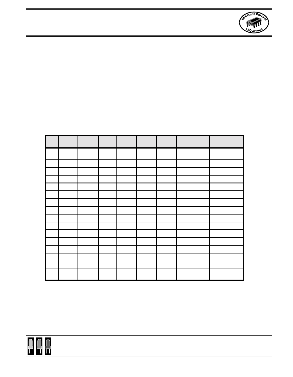
Operation example.
The following example begins with a blank display. Step 1 sets the brightness setting to maximum brightness (15/16 duty cycle). The next step instructs the device to display the character A.
Step 4 instructs the device to display the character B. The next four steps (steps 5 - 8) display
the characters C,D,E and F in sequence, all at full brightness. Step 9 blanks but does not clear
the display and step 10 reprograms the brightness to half (8/16 duty cycle) brightness. Step 11
again displays the character F at half brightness. Step 12 again blanks the device and step 13
programs the character G. Step 14 instructs the device to display the character G (still at the
half brightness setting) and step 15 clears and blanks the display.
STEP D15~D12 D11~D8 D7~D4 D3~D0
0————OffOff
1 0010 0000 XXXX 1111 Off Off Duty=15/16 All Blank
2 0010 0001 0100 0011 Off Off Character Data = A All Blank
3 0001 XXXX XXXX XXXX Off On Normal A
4 0010 0001 0100 0010 On On Character Data = B B
5 0010 0001 0100 0011 On On Character Data = C C
6 0010 0001 0100 0100 On On Character Data = D D
7 0010 0001 0100 0101 On On Character Data = E E
8 0010 0000 0100 0110 On On Character Data = F F
9 0000 XXXX XXXX XXXX Off Off Blank All Blank
10 0010 0000 XXXX 1000 Off Off Duty=8/16 All Blank
11 0001 XXXX XXXX XXXX On On Normal F - Half Brightness
12 0000 XXXX XXXX XXXX Off Off Blank All Blank
13 0010 0000 01 00 0111 Off Off Character Data = G All Blank
14 0001 XXXX XXXX XXXX On On Normal G - Half Brightness
15 0100 XXXX XXXX 0000 Off Off
OUTP UT
R0~R6
OUTP UT
C0~C4
MODE
Initial State
(Clear Mode)
Stand-By
(S hut Do wn)
DISPLAY
INDICATION
All Blank
All Blank
marktech
optoelectronics
For up-to-date product info visit our web site at www.marktechopto.com All specifications subject to change.
Toll Free: (800) 98-4LEDS
120 Broadway • Menands, New York 12204
• Fax: (518) 432-7454
619
TOSHIBA Bi-CMOS Integrated
Circuit Silicon Monolithic
TB62713N/FTB62713N/F
TB62713N/F
TB62713N/FTB62713N/F
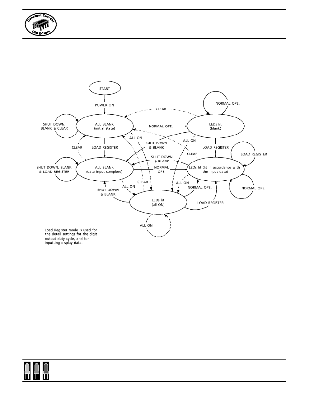
State Movement Diagram
marktech
optoelectronics
For up-to-date product info visit our web site at www.marktechopto.com All specifications subject to change.
620
Toll Free: (800) 98-4LEDS
120 Broadway • Menands, New York 12204
• Fax: (518) 432-7454

TOSHIBA Bi-CMOS Integrated
Circuit Silicon Monolithic
TB62713N/FTB62713N/F
TB62713N/F
TB62713N/FTB62713N/F
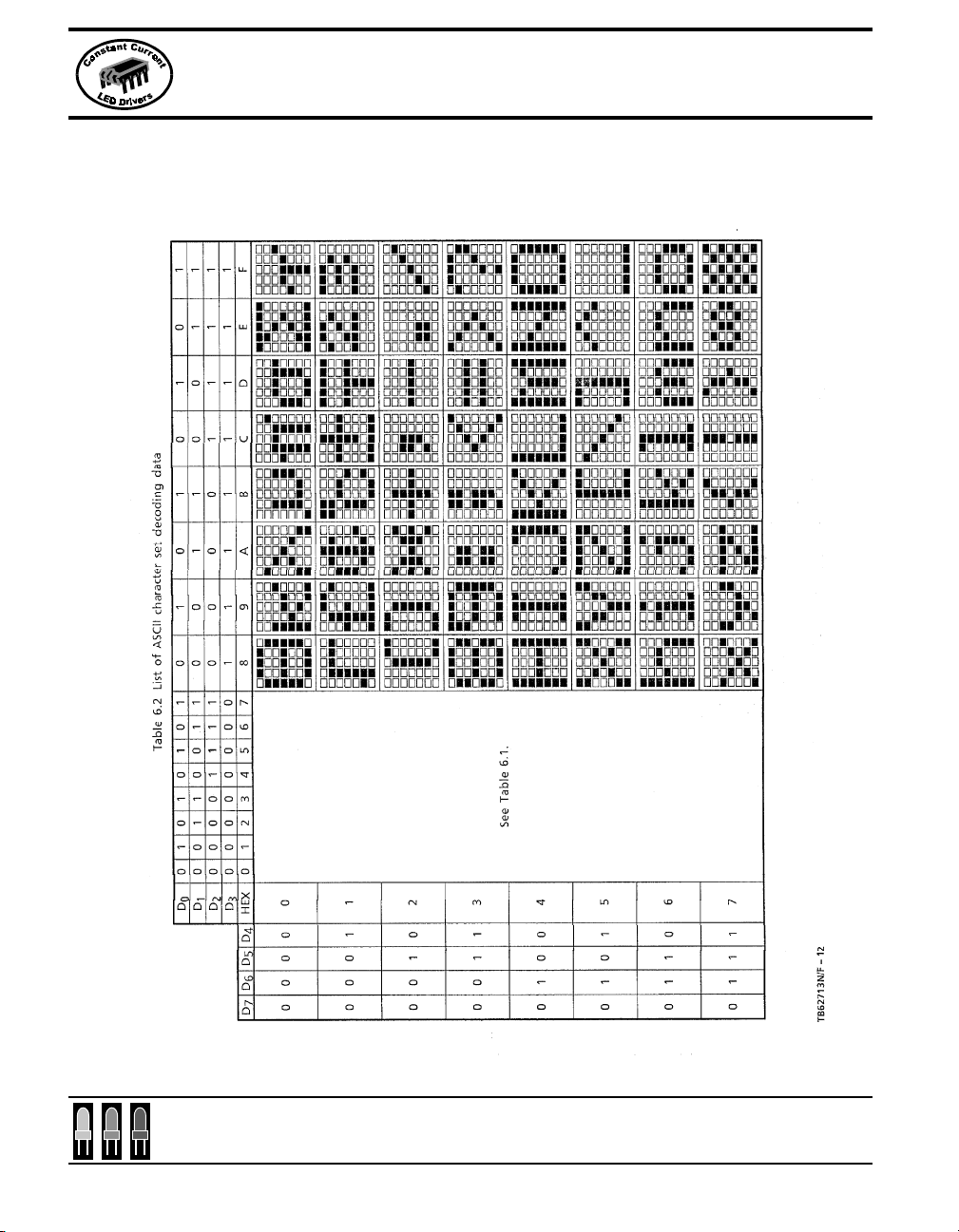
Character Generator List
marktech
optoelectronics
For up-to-date product info visit our web site at www.marktechopto.com All specifications subject to change.
Toll Free: (800) 98-4LEDS
120 Broadway • Menands, New York 12204
• Fax: (518) 432-7454
621
TOSHIBA Bi-CMOS Integrated
Circuit Silicon Monolithic
TB62713N/FTB62713N/F
TB62713N/F
TB62713N/FTB62713N/F
Character Generator List
marktech
optoelectronics
For up-to-date product info visit our web site at www.marktechopto.com All specifications subject to change.
622
Toll Free: (800) 98-4LEDS
120 Broadway • Menands, New York 12204
• Fax: (518) 432-7454

TOSHIBA Bi-CMOS Integrated
Circuit Silicon Monolithic
TB62713N/FTB62713N/F
TB62713N/F
TB62713N/FTB62713N/F
Test Circuit:
marktech
optoelectronics
For up-to-date product info visit our web site at www.marktechopto.com All specifications subject to change.
Toll Free: (800) 98-4LEDS
120 Broadway • Menands, New York 12204
• Fax: (518) 432-7454
623

TOSHIBA Bi-CMOS Integrated
Circuit Silicon Monolithic
TB62713N/FTB62713N/F
TB62713N/F
TB62713N/FTB62713N/F
Test Circuit:
marktech
optoelectronics
For up-to-date product info visit our web site at www.marktechopto.com All specifications subject to change.
624
Toll Free: (800) 98-4LEDS
120 Broadway • Menands, New York 12204
• Fax: (518) 432-7454

TOSHIBA Bi-CMOS Integrated
Circuit Silicon Monolithic
TB62713N/FTB62713N/F
TB62713N/F
TB62713N/FTB62713N/F
Test Circuit:
marktech
optoelectronics
For up-to-date product info visit our web site at www.marktechopto.com All specifications subject to change.
Toll Free: (800) 98-4LEDS
120 Broadway • Menands, New York 12204
• Fax: (518) 432-7454
625

TOSHIBA Bi-CMOS Integrated
Circuit Silicon Monolithic
TB62713N/FTB62713N/F
TB62713N/F
TB62713N/FTB62713N/F
Graphs:
marktech
optoelectronics
For up-to-date product info visit our web site at www.marktechopto.com All specifications subject to change.
626
Toll Free: (800) 98-4LEDS
120 Broadway • Menands, New York 12204
• Fax: (518) 432-7454

TOSHIBA Bi-CMOS Integrated
Circuit Silicon Monolithic
TB62713N/FTB62713N/F
TB62713N/F
TB62713N/FTB62713N/F
Outline Drawings:
marktech
optoelectronics
For up-to-date product info visit our web site at www.marktechopto.com All specifications subject to change.
Toll Free: (800) 98-4LEDS
120 Broadway • Menands, New York 12204
• Fax: (518) 432-7454
627
 Loading...