

TOSHIBA Bi-CMOS Integrated
Circuit Silicon Monolithic
TB62709N/FTB62709N/F
TB62709N/F
TB62709N/FTB62709N/F
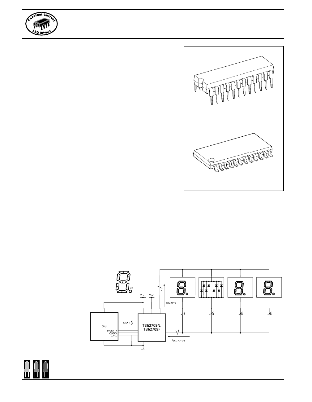
Intelligent, Constant Current, 7 segment LED numeric display
decoder/driver. For use with common anode configuration
numeric displays.
The TB62709N/F is an intelligent Constant Current LED display
driver designed specifically for seven segment LED display applications. The stand alone device includes all of the decode,
multiplex and driver circuitry necessary to control up to four seven
segment LED digits. All of the information required to program
up to four LED digits is input serially including a 16 step brightness control. Expansion beyond four digits is possible with a
cascade connection to a second device. The device automatically refreshes and maintains the displayed information.
Features
• Constant Current segment drivers for consistent display
brightness.
• Single device saves labor and board space.
• Internal character set simplifies design efforts.
• Automatically handles multiplex and display refresh tasks.
• 16 step programmable brightness control.
• Single device controls up to four digits.
• Available in thru hole and surface mount packages.
• Data out cascade port for expansion beyond four digits.
TB62709N
SDIP24-P-300-1.78 Weight: 1.62g (Typ.)
TB62709F
SSOP24-P-300-1.00 Weight: 0.32g (Typ.)
Performance Characteristics
VDD = 4.5V~5.5V
Digit enable: 17V / 400mA
Segment select: 17V / 0-40mA
Max transition frequency: 15Mhz
marktech
optoelectronics
For up-to-date product info visit our web site at www.marktechopto.com All specifications subject to change.
584
Toll Free: (800) 98-4LEDS
120 Broadway • Menands, New York 12204
• Fax: (518) 432-7454
TOSHIBA Bi-CMOS Integrated
Circuit Silicon Monolithic
TB62709N/FTB62709N/F
TB62709N/F
TB62709N/FTB62709N/F
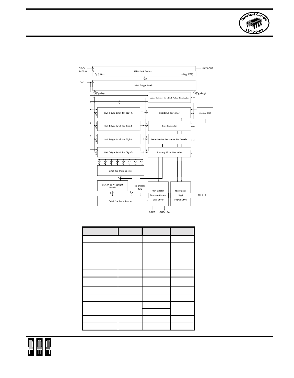
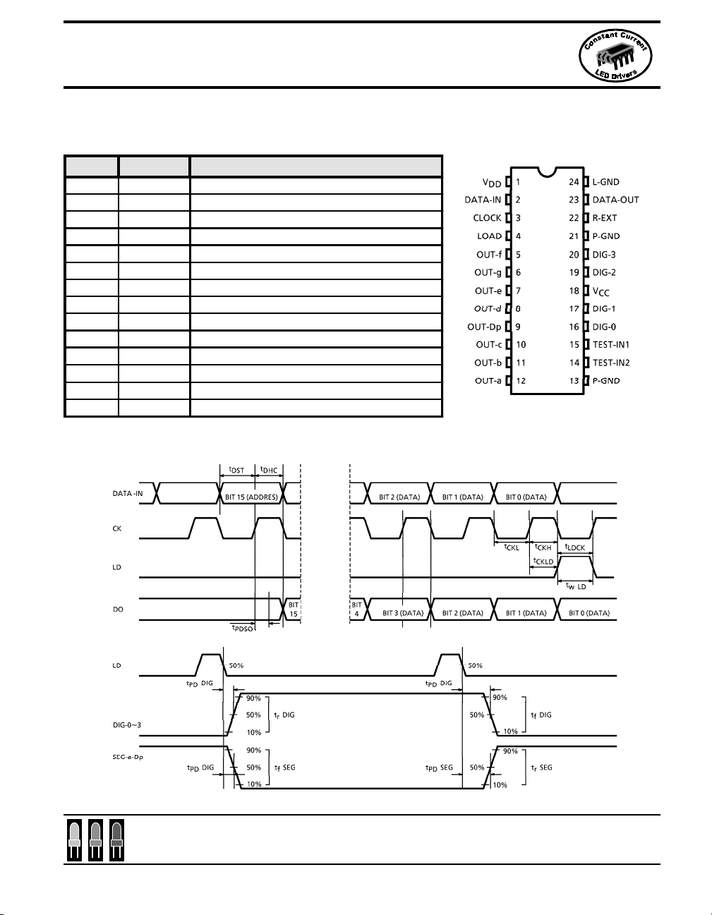
Block Diagram:
Maximum Ratings:
CHAR ACTERIST ICS SYMBOL RATING UNIT
Sup ply Volt ag e VD D 7.0 volt s
LED Supply Voltage VCC 17 volts
Sourc e Output C urrent
Digit 0~3
Segment Drive Current
Segment a~DP
Output Curre nt IOH/IOL +/- 5 mA
Inp ut V o lta ge V IN
Clock Frequency FCLK 15 MHz
Total Outp ut Cur rent IVD D 40 0 mA
Power Dissipation PD
Operation Temperature Topr -40 ~ +85 °C
Storage Temperature Tstg -55 ~+150 °C
marktech
optoelectronics
For up-to-date product info visit our web site at www.marktechopto.com All specifications subject to change.
ID IG -40 0 m A
IOU T 5 0 m A
-0.3 ~ VD D
~+0.3
TB62709N: 1.78
TB62709F: 0.62
volts
120 Broadway • Menands, New York 12204
Toll Free: (800) 98-4LEDS
W
• Fax: (518) 432-7454
585
TOSHIBA Bi-CMOS Integrated
Circuit Silicon Monolithic
TB62709N/FTB62709N/F
TB62709N/F
TB62709N/FTB62709N/F
Recommended Operating Conditions:
CHAR ACTER IST ICS SYMBOL
Output Stage
Supply Current ICC1 1
IC C2 1
Digit 0~3 Scanning Freq. fOSC 2
Out a~DP Output Current ISEG 3
Digit 0~3 Leakage Current ILEAK1 4 All off mode, VCC=17V — — -20 µA
Out a~DP Leakage Current ILEAK2 4 All off mode, VCC=17V — — 20 µA
Digit 0~3 Output Voltage VOUT 5
Logic
Supply Current
Operating Supply Current IDD3 6
High Level Input Current IIH — Data-in, Load& Clock VIN=5V — — 1 µA
Low Level Output Current IIL — Data-in, Load&Clock VIN=0V — — -1 µA
High Le vel Output Voltage
Low Level Output Voltage
Clock Frequency FCLK 6
IDD1 6 Standby Mode, Ta=25°C — — 200 µA
IDD2 6 Blank Mode, Ta=25°C — — 12.5 mA
VOH1 6 Data out, IOH=-1mA 4.6 — — V
VOH2 6 Data-out, IOH=-1µA — VDD — V
VOL1 6 Data out, IOH=-1mA — — 0.4 V
VOL2 6 Data-out, IOH=-1µA — 0.1 — V
TEST
CIRCUIT
CONDITION MIN. TYP. MAX. UNIT
Set normal operation mode,
Ω,
Rext=760
ON VCC = 5V, Ta=25°C
Set normal operation mode,
Rext=760
ON VCC = 5V, Ta=25°C
Normal operation mode,
VDD=4.5 - 5.5V
Normal operation mode,
VDD=4.5 - 5.5V
Normal operation mode
ID IG = 3 20 mA
Normal operating mode
fCLK=10MHz, Ta=25°C
Data-i n:output a~DP o n
CASCADE connected,
TA = -40 ~ 85ºC
Out a~DP, all
Ω,
Out a~DP, all
—300—mA
—320—mA
240 480 960 Hz
29 34 40 mA
3.0 — — V
— — 20.5 mA
10 — — MHz
marktech
optoelectronics
For up-to-date product info visit our web site at www.marktechopto.com All specifications subject to change.
Toll Free: (800) 98-4LEDS
120 Broadway • Menands, New York 12204
• Fax: (518) 432-7454
586
TOSHIBA Bi-CMOS Integrated
Circuit Silicon Monolithic
TB62709N/FTB62709N/F
TB62709N/F
TB62709N/FTB62709N/F
Switching Characteristics:
CH ARACTER ISTICS SYMBOL CONDITION MIN. TYP. MAX. UNIT
Data Hold Time (D-IN Clock) tDHO — 10 — ns
Data Set-up Time (D-IN Clock) tDS T — 20 — ns
Propagation Delay (Clock D-OUT)
High Level Pulse Wi dth Of Clock tCLK H — 30 — ns
Low Level Pulse Width Of Clock tCLKL — 30 — ns
Pulse Width Of Load tw LD — 100 — ns
Setup Time (Clock-Load) tCLK-LD — 50 — ns
Setup Time (Load-Clock) tLD-CLK — 50 — ns
Out a ~ DP Propagation Delay
(Load-Outn)
Out a ~ DP Rise Time (OUTn) trSEG CL=10pf 0.2 1.0 — µs
Out a ~ DP Fall Time (OUTn) tfSEG CL=10pf 0.2 1.0 — µs
Digit 0 ~ 3 Propagation Delay
(Load-DIGn)
Digit 0 ~ 3 Rise Time (DIGn) trDIG CL=10pf 0.4 2.0 — µs
Digit 0 ~ 3 Fall Time (DIGn) tfDIG CL=10pf 0.4 2.0 — µs
tPHL-SO CL=10pf — 25 — ns
tPLH-SO CL=10pf — 25 — ns
tpHL-S EG CL=1 0pf — — 5.0 ns
tpLH-SEG CL=10pf — — 5.0 ns
tpHL-D IG CL=10pf — — 10.0 µs
tpLH-DIG CL=10pf — — 10.0 µs
marktech
optoelectronics
For up-to-date product info visit our web site at www.marktechopto.com All specifications subject to change.
Toll Free: (800) 98-4LEDS
120 Broadway • Menands, New York 12204
• Fax: (518) 432-7454
587
TOSHIBA Bi-CMOS Integrated
Circuit Silicon Monolithic
TB62709N/FTB62709N/F
TB62709N/F
TB62709N/FTB62709N/F
Recommended Operating Conditions:
CHARACTERISTICS SYMBOL CONDITION MIN. TYP. MAX. UNIT
Output Sta ge
Supply Voltage VCC 4.0 — 6.0 V
Digit 0~3 Output Current IDIG VOUT=3.0V — — -320 mA
Out a~DP Output Current ISEG VCE=0.7V — — 40 mA
Logic
Supply Voltage VDD 4.5 — 5.5 V
High Level Input Current IIH
Low Level Input Current IIL Data-In, Load&Clock,VIN=0V — — -1 µA
High Level Input Voltage VIH
Low Level Input Voltage VIL — —
Switching Condition
Data Hold Time (D-IN Clock) tDHO 30 — — ns
Data Setup Time (D-IN Clock ) tDST 50 — — ns
Propagation Delay (Clock D-Out) tPDSO CL=10pf 50 — — ns
High Level Pulse Width Of Clock tCLKH 30 — — ns
Low Level Pulse Width Of Clock tCLKL 30 — — ns
Pulse Width Of Load twLD 150 — — ns
Setup Time (Clock-Load) tCKLD 100 — — ns
Setup Time (Load-Clock) tLDCLK 100 — — ns
Data-In,
Load&Clock,VIN=VDD
—— 1µA
0.7
—— V
VDD
0.3
V
VDD
marktech
optoelectronics
For up-to-date product info visit our web site at www.marktechopto.com All specifications subject to change.
588
Toll Free: (800) 98-4LEDS
120 Broadway • Menands, New York 12204
• Fax: (518) 432-7454
TOSHIBA Bi-CMOS Integrated
Circuit Silicon Monolithic
TB62709N/FTB62709N/F
TB62709N/F
TB62709N/FTB62709N/F
Terminal Description:
PIN No. NAME FUNCTION
1V
2 Serial Data IN (SI) Serial Data Input To Shift Register
3 Clock (CK) Clock Input Terminal
4 Load (LD) Load Input Terminal
5-12 OUT a~DP Output Terminal to Cathodes of Seven Segment Display
13 P-GND Power Ground Terminal
14 Test In 2 Test Terminal - Grounded During Normal Operation
15 Test In 1 Test Terminal - Grounded During Normal Operation
6,17,19,2 Digit 0~3 Output Terminal to Anodes of Seven Segment Display
18 V
21 P-GND Power Ground Terminal
22 Rext Constant Current Progra mming Terminal
23 Data Out (DO) Cascade Connection To Next Display Stage
24 L-GND Logi c Ground Terminal
Timing Diagram:
DD
CC
Logic Supply Voltage
Supply Voltage For LEDs
marktech
optoelectronics
For up-to-date product info visit our web site at www.marktechopto.com All specifications subject to change.
Toll Free: (800) 98-4LEDS
120 Broadway • Menands, New York 12204
• Fax: (518) 432-7454
589
TOSHIBA Bi-CMOS Integrated
Circuit Silicon Monolithic
TB62709N/FTB62709N/F
TB62709N/F
TB62709N/FTB62709N/F
Data Input
Data is input on the SERIAL-IN terminal. Each 16 bit serial word includes an address (D15 ~ D8)
and data (D7 ~ D0). A low to high transition load command on the LOAD terminal loads the data
into the appropriate registers following the 16th clock pulse.
Operation
Serial data is input on the DATA-IN terminal beginning with the most significant bit (MSB). Data
is clocked through the 16 bit shift register on the rising edge of the clock. A Low to High transition on the LOAD input following the 16th (LSB) bit latches the 16 bit word into the 16 bit D-type
latch.
Expansion beyond four digits is possible through the use of a cascade connection from the
DATA-OUT terminal. The data-out lags data-in by one bit through the data-out terminal.
Each 16 bit word typically includes 8 address bits and 8 data bits. The first four data bits,
beginning with D15 (MSB) ~ D12 select the Action mode (see figure 1). These global commands determine the overall function the device is to perform and includes Blank, Normal
Operation, Load Register, All On and Stand-by. Data bits D11~D8 select the particular register to
be loaded (see figure 2) should the load register function be selected. Data bits D7~D0 (LSB)
define the specific commands required to program the display and define the brightness setting
(duty cycle).
Figure 1. Action Mode
FUNCTION
Blank
(OUTn & Dig it 0~3 All Off)
Normal Operation 0 0 0 1 — — — 1 - - - H
Load Register
(Duty, Decode, Digit & Data)
All On (OUTn ALL On) 0 0 1 1 — — — 3 - - - H
Stand-By 0 1 0 0 — — — 4 - - - H
REGISTER DATA
D15 D14 D13 D12 D11~D8 D7~D4 D3~D0 Hex Code
0 0 0 0 — — — 0 - - - H ⇐
0 0 1 0 X X X 2 xxx H
INITIAL
STATE
“x” indicates that data is required in this field to execute the function. “-” indicates that data in
this field is not required and not recognized.
marktech
optoelectronics
For up-to-date product info visit our web site at www.marktechopto.com All specifications subject to change.
590
Toll Free: (800) 98-4LEDS
120 Broadway • Menands, New York 12204
• Fax: (518) 432-7454
TOSHIBA Bi-CMOS Integrated
Circuit Silicon Monolithic
TB62709N/FTB62709N/F
TB62709N/F
TB62709N/FTB62709N/F
Action Mode
1. Blank - Constant current segment drivers are off resulting in an all segments off condition.
Data D15 ~ D12 are 0. D11~D0 are not relevent in blank mode.
2. Normal (Operation) - Instructs device to display data loaded during previous steps. D11~ D0
are not relevent in the Normal Operation mode.
3. Load Register - Directs the device to recognize and load D11~ D0. In this mode D11 ~ D8
determines the specific register to be loaded (see figure 2) and D7 ~ D0 serves as the actual
data to be loaded for programming the brightness (duty cycle) or the particular digit.
4. All On - All constant current segment drivers are on resulting in an all segments illuminated
condition. D11 ~ D0 are not relevent in this mode.
5. Stand By - All display segments off condition. The Stand-By command turns off all internal
bias currents and serves as a low power consumption mode (<.2mA). Used with Stand-By set
up commands “All Data Clear” or “Data Not Cleared” (table 7).
The initial state, upon power up, is the BLANK state.
Application Note:
Stand-By and Blank perform similar functions in that the display is totally blank when either
command is input. Stand-By provides a low power consumption (<.2ma current draw on VDD)
mode by turning off all internal bias currents in the internal driver circuits. The Stand-By command also cuts off the Rext bias current used to regulate the programmed constant current
within the device.
marktech
optoelectronics
For up-to-date product info visit our web site at www.marktechopto.com All specifications subject to change.
Toll Free: (800) 98-4LEDS
120 Broadway • Menands, New York 12204
• Fax: (518) 432-7454
591

TOSHIBA Bi-CMOS Integrated
Circuit Silicon Monolithic
TB62709N/FTB62709N/F
TB62709N/F
TB62709N/FTB62709N/F
LOAD REGISTER Mode
Figure 2. LOAD REGISTER Mode
REGISTER DATA
FUNCTION
Load Duty Register 2H 0 0 0 0 X X 20XXH
Load Decode & Digit Register 2H 0 0 0 1 X X 21XXH
Load Data Register 0 2H 0 0 1 0 X X 22XXH
Load Data Register 1 2H 0 0 1 1 X X 23XXH
Load Data Register 2 2H 0 1 0 0 X X 24XXH
Load Data Register 3 2H 0 1 0 1 X X 25XXH
“x” indicates that data is required in this field to execute the function. “-” indicates that data in
this field is not required and not recognized.
Selects the specific register to be loaded. The LOAD REGISTER mode is enabled by the Load
Register Action mode command (see Figure 1 - Action mode).
D15~D12 D11 D10 D9 D8 D7~D4 D3~D0 Hex Code
1. Duty Register - Enables the device to accept duty cycle (brightness) setting. Sixteen brightness steps (0/16 to 15/16) are available.
2. Decode and Digit Register - Enables the device to accept data defining digit or digits to be
programmed.
3. Data Register 0~3 - Commands the device to enable a specific digit register to accept the
data to be displayed on the selected digit. Actual display data is set up by D7~D0.
marktech
optoelectronics
For up-to-date product info visit our web site at www.marktechopto.com All specifications subject to change.
592
Toll Free: (800) 98-4LEDS
120 Broadway • Menands, New York 12204
• Fax: (518) 432-7454

TOSHIBA Bi-CMOS Integrated
Circuit Silicon Monolithic
TB62709N/FTB62709N/F
TB62709N/F
TB62709N/FTB62709N/F
Data Decode
The TB62709F utilizes two basic modes of operation. In the DECODE MODE, data encoded in
data bits D7~D0 is decoded to display preset characters per table 8. This mode is activated as
illustrated in table 5. With D15~D8 programmed as 21 Hex and D7~D4 as 1 Hex the DECODE
MODE is selected.
In the DIRECT DRIVE MODE the ability to decode data to preset characters for display is
bypassed giving the programmer direct control of the 8 constant current sink outputs. This mode
may be used to drive discrete LEDs or to display characters not included in the character set.
REGISTER DATA
FUNCTION
Direct Drive 21H 0 0 0 0 X 210XH
Decode 21H 0 0 0 1 X 211XH
D15~D8 D7 D6 D5 D4 D3~D0 Hex Code
INITIAL
STATE
⇐
“x” indicates that data is required in this field to execute the function. “-” indicates that data in
this field is not required and not recognized.
This programming step is performed simultaneously with the DIGIT SELECTION decision (table
4) which utilizes D3~D0.The initial state, upon power up, is the DECODE mode.
Table below illustrates the input / output relationship in the DIRECT DRIVE mode. A Logic 1
data state turns the respective output on and a Logic 0 data state turns the respective output off.
REGISTER DATA OUTP UT IN ITIAL STATE NOTE
D0 Out-a L
D1 Out-b L
D2 Out-c L
D3 Out-d L
D4 Out-e L
D5 Out-f L
D6 Out-g L
D7 Out-DP L
H Dat a is
output ON (1)
and
L Data is
output OFF (0)
marktech
optoelectronics
For up-to-date product info visit our web site at www.marktechopto.com All specifications subject to change.
Toll Free: (800) 98-4LEDS
120 Broadway • Menands, New York 12204
• Fax: (518) 432-7454
593

TOSHIBA Bi-CMOS Integrated
Circuit Silicon Monolithic
TB62709N/FTB62709N/F
TB62709N/F
TB62709N/FTB62709N/F
Brightness Control
Brightness is controlled by controlling the “on time” duty cycle. The device allows for 16 brightness steps as illustrated in list 3 with 0/16 as the dimmest setting (not illuminated) to 15/16 as
the brightest setting. The duty cycle control register is addressed with a 20 Hex command at
D15~D8 and the appropriate data per list 3 at D3~D0. D7~D4 are not recognized by the duty
cycle register. The initial state, upon power up is 15/16, or full brightness.
REGISTER DATA
Duty Cycle
0/16 20H — 0 0 0 0 20X0H
1/16 20H — 0 0 0 1 20X1H
2/16 20H — 0 0 1 0 20X2H
3/16 20H — 0 0 1 1 20X3H
4/16 20H — 0 1 0 0 20X4H
5/16 20H — 0 1 0 1 20X5H
6/16 20H — 0 1 1 0 20X6H
7/16 20H — 0 1 1 1 20X7H
8/16 20H — 1 0 0 0 20X8H
9/16 20H — 1 0 0 1 20X9H
10/16 20H — 1 0 1 0 20XAH
11/16 20H — 1 0 1 1 20XBH
12/16 20H — 1 1 0 0 20XCH
13/16 20H — 1 1 0 1 20XDH
14/16 20H — 1 1 1 0 20XEH
15/16 20H — 1 1 1 1 20XFH
D15~D8 D7~D4 D3 D2 D 1 D0 Hex Code
INIT IAL
STATE
⇐
“x” indicates that data is required in this field to execute the function. “-” indicates that data in
this field is not required and not recognized.
marktech
optoelectronics
For up-to-date product info visit our web site at www.marktechopto.com All specifications subject to change.
594
Toll Free: (800) 98-4LEDS
120 Broadway • Menands, New York 12204
• Fax: (518) 432-7454

TOSHIBA Bi-CMOS Integrated
Circuit Silicon Monolithic
TB62709N/FTB62709N/F
TB62709N/F
TB62709N/FTB62709N/F
Digit Selection
The digit(s) to be programmed are selected as illustrated table below. This function is enabled
with a 21 Hex command at D15~D8 and the appropriate data sequence to select Digit 0 only,
Digit 0 and 1, Digit 0 -2 or digit 0-3 as illustrated in table 4. This programming step is performed
simultaneously with the DECODE / DIRECT DRIVE decision (table 5) which utilizes D7~D4. The
initial state, upon power up, is Digits 0-3 activated.
REGISTER DATA
D15~D8 D7~D4 D3 D2 D1 D0 Hex Code
Activate Digit 0 Only 21H X 0 0 0 0 21X0H
Activate Digit 0~1 21H X 0 0 0 1 21X1H
Activate Digit 0~2 21H X 0 0 1 0 21X 2H
Activate Digit 0~3 21H X 0 0 1 1 21X 3H
INITIAL
STATE
⇐
STAND-BY Commands
Two STAND-BY commands are available as illustrated in table below. STAND-BY / NO DATA
CLEAR places the device in a power save mode while leaving data intact in the various registers. This mode is enabled by a 4 Hex command at D15~D12 and 0 Hex at D3~D0. D11~D4 are
not relevent in the STAND-BY / NO DATA CLEAR Mode.
STAND-BY / DATA CLEAR also places the device in a power save mode and clears data in the
various registers leaving registers in their initial state. This mode is enabled by a 4 Hex command at D15~D12 and 1 Hex at D3~D0. D11~D4 are not relevent in the STAND-BY / DATA
CLEAR Mode.
REGISTER DATA
D15~D8 D7~D4 D3 D2 D1 D0 Hex Code
Stand-By (No Data Clear) 4-H — 0 0 0 0 4XX0H
Stand-By (Data Clear) 4-H — 0 0 0 1 4XX1H
“x” indicates that data is required in this field to execute the function. “-” indicates that data in
this field is not required and not recognized.
marktech
optoelectronics
For up-to-date product info visit our web site at www.marktechopto.com All specifications subject to change.
Toll Free: (800) 98-4LEDS
120 Broadway • Menands, New York 12204
• Fax: (518) 432-7454
595

TOSHIBA Bi-CMOS Integrated
Circuit Silicon Monolithic
TB62709N/FTB62709N/F
TB62709N/F
TB62709N/FTB62709N/F
CHARACTER DECODE Mode
Table 8 illustrates the data versus character displayed relationship. This mode is enabled along
with the LOAD REGISTER Mode (See LOAD REGISTER Mode section - Figure 2). A 2 Hex
command at D15~D12 selects the LOAD REGISTER Mode. The specific register to be addressed is selected by D11~D8. The digits are designated D0, D1, D2 and D3 and are addressed per their respective registers as illustrated in Figure 2. D3~D0 provides the code for the
seven segment display. D5 and D4 select one of two character sets and D6 controls the decimal
point for each digit.
marktech
optoelectronics
For up-to-date product info visit our web site at www.marktechopto.com All specifications subject to change.
596
Toll Free: (800) 98-4LEDS
120 Broadway • Menands, New York 12204
• Fax: (518) 432-7454
TOSHIBA Bi-CMOS Integrated
Circuit Silicon Monolithic
TB62709N/FTB62709N/F
TB62709N/F
TB62709N/FTB62709N/F
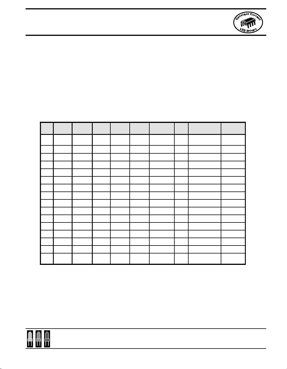
Operation examples.
Example 1
Example 1 sets up the character a at Digit 0, b at Digit 1, c at Digit 2 and d at Digit 3. The
characters are initially set at full brightness (15/16 duty cycle) and displayed. The duty cycle is
then changed to half brightness (8/16 duty cycle) as the display is first blanked and then activated with the same a,b,c and d characters. The display is then flashed on and off by alternating
the BLANK and NORMAL commands before going to the STAND-BY Mode.
STEP D15~D12 D11~D8 D7~D4 D3~D0 DIGIT 0~3
0————Off OffOff
1 0010 0000 XXXX 1111 Off Off Off Duty=15/16 All Blank
2 0010 0001 0001 0011 Off Off Off Decode 4 Dig. All Blank
3 0010 0010 X000 1010 Off Off Off Dig 0=a All Blank
4 0010 0011 X000 1011 Off Off Off Di g 1=b All Blank
5 0010 0100 X000 1100 Off Off Off Di g 2=c All Blank
6 0010 0101 X000 1101 Off Off Off Dig 3=d All Blank
7 0001 XXXX XXXX XXXX On On Off Normal a-b-c-d
8 0010 0000 XXX X 1000 On On Off Duty=8/16 a-b-c-d
9 0000 XXXX XXXX XXXX Off Off Off Blank All Blank
10 0001 XXXX XXXX XX XX On On Off Normal a-b-c-d
11 0000 XXXX XXXX XXXX Off Off Off Blank All Blank
12 0001 XXXX XXXX XX XX On On Off Normal a-b-c-d
13 0000 XXXX XXXX XXX X Off Off Off Blank All Blank
14 0001 XXXX XXXX XX XX On On Off Normal a-b-c-d
15 01 00 XXXX X XXX 0000 Off Off Off
SEGMENT
a,b,c,d,e,f,g
SEG
DP
MODE
Initial State (Clear
Mode)
Stand-By
(Shut Down)
DISPLAY
INDICATION
All Blank
All Blank
marktech
optoelectronics
For up-to-date product info visit our web site at www.marktechopto.com All specifications subject to change.
Toll Free: (800) 98-4LEDS
120 Broadway • Menands, New York 12204
• Fax: (518) 432-7454
597

TOSHIBA Bi-CMOS Integrated
Circuit Silicon Monolithic
TB62709N/FTB62709N/F
TB62709N/F
TB62709N/FTB62709N/F
Operation examples.
Example 2
Example 2 sets up the character a with the decimal point on at Digit 0 at full brightness (15/16
duty cycle) with the remaining digits (1~3) left blank. The display then changes to a character b
with the decimal point on displayed at Digit 1 with Digits 0, 2 and 3 blank. Character c (decimal
point on) is then displayed at Digit 2 with Digits 0, 1 and 3 left blank and the sequence ends with
the character d (decimal point on) displayed on Digit 3 with Digits 0~2 left blank followed by the
STAND-BY Mode.
STEP D15~D12 D11~D8 D7~D4 D3~D0 DIGIT 0~3
0 — — — — Off Off Off
1 00 10 0000 XX XX 1111 Off Off Off Duty=15/16 All Bla nk
2 0010 0001 0001 0011 Off Off Off Decode 4 Dig. All Blank
3 0010 0010 X100 1010 Off Off Off Dig 0=a All Blank
4 0010 0011 X001 0000 Off Off Off Dig 1=Blank All Blank
5 0010 0100 X001 0000 Off Off Off Dig 2=Blank All Blank
6 0010 0101 X001 0000 Off Off Off Dig 3=Blank All Blank
7 0001 XXXX XXXX XXXX On On Off Normal a - - -
8 0010 0010 X001 0000 Off On Off Dig 0=Blank All Blank
9 0010 0011 X100 1011 On On Off Dig 1=b - b - -
10 0010 0011 X001 0000 Off On Off D ig 1=Blank All Blank
11 0010 0100 X1 00 1100 On On Off Dig 2=c - - c -
12 0010 0100 X0 01 0000 Off On Off D ig 2=Blank All Blank
13 0010 01 01 X100 1101 On On Off D ig 3=d - - - d
14 010 0 XX XX XX XX 00 00 Off Off Off
SEGMENT
a,b,c,d,e,f,g
SEG
DP
MODE
Initial State (Clear
Mode)
Stand-By
(Shut Down)
DISPLAY
IND ICATION
All Bla nk
All Bla nk
marktech
optoelectronics
For up-to-date product info visit our web site at www.marktechopto.com All specifications subject to change.
598
Toll Free: (800) 98-4LEDS
120 Broadway • Menands, New York 12204
• Fax: (518) 432-7454

TOSHIBA Bi-CMOS Integrated
Circuit Silicon Monolithic
TB62709N/FTB62709N/F
TB62709N/F
TB62709N/FTB62709N/F
State Movement Diagram
marktech
optoelectronics
For up-to-date product info visit our web site at www.marktechopto.com All specifications subject to change.
Toll Free: (800) 98-4LEDS
120 Broadway • Menands, New York 12204
• Fax: (518) 432-7454
599

TOSHIBA Bi-CMOS Integrated
Circuit Silicon Monolithic
TB62709N/FTB62709N/F
TB62709N/F
TB62709N/FTB62709N/F
Test Circuit
marktech
optoelectronics
For up-to-date product info visit our web site at www.marktechopto.com All specifications subject to change.
600
Toll Free: (800) 98-4LEDS
120 Broadway • Menands, New York 12204
• Fax: (518) 432-7454

TOSHIBA Bi-CMOS Integrated
Circuit Silicon Monolithic
TB62709N/FTB62709N/F
TB62709N/F
TB62709N/FTB62709N/F
Test Circuit
marktech
optoelectronics
For up-to-date product info visit our web site at www.marktechopto.com All specifications subject to change.
Toll Free: (800) 98-4LEDS
120 Broadway • Menands, New York 12204
• Fax: (518) 432-7454
601

TOSHIBA Bi-CMOS Integrated
Circuit Silicon Monolithic
TB62709N/FTB62709N/F
TB62709N/F
TB62709N/FTB62709N/F
Test Circuit
marktech
optoelectronics
For up-to-date product info visit our web site at www.marktechopto.com All specifications subject to change.
602
Toll Free: (800) 98-4LEDS
120 Broadway • Menands, New York 12204
• Fax: (518) 432-7454

TOSHIBA Bi-CMOS Integrated
Circuit Silicon Monolithic
TB62709N/FTB62709N/F
TB62709N/F
TB62709N/FTB62709N/F
Duty Cycle Control vs. Output Current Value:
marktech
optoelectronics
For up-to-date product info visit our web site at www.marktechopto.com All specifications subject to change.
Toll Free: (800) 98-4LEDS
120 Broadway • Menands, New York 12204
• Fax: (518) 432-7454
603

TOSHIBA Bi-CMOS Integrated
Circuit Silicon Monolithic
TB62709N/FTB62709N/F
TB62709N/F
TB62709N/FTB62709N/F
External Resister vs. Output Current Value:
marktech
optoelectronics
For up-to-date product info visit our web site at www.marktechopto.com All specifications subject to change.
604
Toll Free: (800) 98-4LEDS
120 Broadway • Menands, New York 12204
• Fax: (518) 432-7454

TOSHIBA Bi-CMOS Integrated
Circuit Silicon Monolithic
TB62709N/FTB62709N/F
TB62709N/F
TB62709N/FTB62709N/F
Cascade Operation:
DIG 0-3
Dat a In
Vcc
Clo ck
LOAD
4
TB62 709 a~D p
Dat a O ut
Vcc
Dat a In
TB62 709 a~D p
Dat a O ut
Vcc
Dat a In
TB62 709 a~D p
8
4
8
DIG 8-11
4
8
DIG 4-74444
4444
8888
8888
4444
8888
In order to update the display information within a specific driver
perform the following actions as appropriate.
Case 1. Digit 0–3:
Input 16 bit data serially, Pulse Load Line High Once
Case 2. Digit 4-7:
Input 32 bits of data that corresponds to the information to be displayed on Digits 0-3 + Digits 4-7 (most significant)
then Pulse Load Line High Once
Case 3. Digit 8-11:
Input 48 bits of data that corresponds to the information to be displayed on Digits 0-3 + Digits 4-7 + Digits 8-11 (most
significant) then Pulse Load Line High Once
marktech
optoelectronics
For up-to-date product info visit our web site at www.marktechopto.com All specifications subject to change.
Toll Free: (800) 98-4LEDS
120 Broadway • Menands, New York 12204
• Fax: (518) 432-7454
605

TOSHIBA Bi-CMOS Integrated
Circuit Silicon Monolithic
TB62709N/FTB62709N/F
TB62709N/F
TB62709N/FTB62709N/F
Outline:
marktech
optoelectronics
For up-to-date product info visit our web site at www.marktechopto.com All specifications subject to change.
606
Toll Free: (800) 98-4LEDS
120 Broadway • Menands, New York 12204
• Fax: (518) 432-7454

TOSHIBA Bi-CMOS Integrated
Circuit Silicon Monolithic
TB62709N/FTB62709N/F
TB62709N/F
TB62709N/FTB62709N/F
Outline:
marktech
optoelectronics
For up-to-date product info visit our web site at www.marktechopto.com All specifications subject to change.
Toll Free: (800) 98-4LEDS
120 Broadway • Menands, New York 12204
• Fax: (518) 432-7454
607
 Loading...