

TT
OSHIBOSHIB
T
OSHIB
TT
OSHIBOSHIB
A Bi-CMOSA Bi-CMOS
A Bi-CMOS
A Bi-CMOSA Bi-CMOS
Constant CurConstant Cur
Constant Cur
Constant CurConstant Cur
rr
ent Interfent Interf
r
ent Interf
rr
ent Interfent Interf
ace Driace Dri
ace Dri
ace Driace Dri
vv
v
vv
erer
er
erer
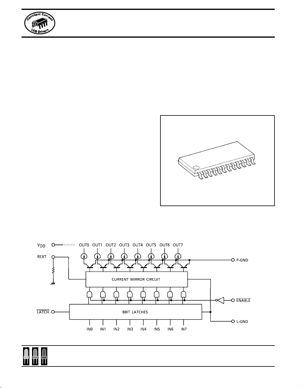
TB62707F
8 Bit Constant Current LED Driver with Latch Function
Product Description:
The TB62707F is specifically designed for LED display applications. The Bi-CMOS device has 8
Bi-polar constant current output channels and includes CMOS latch function.
The LED drive current is programmed by the
installation of a single resistor per device.
Current is programmable from 5-90mA and is
held constant across all 8 outputs effectively
compensating for the inherent circuit and
component variables which affect the brightness
of the LEDs.
Features:
• 8 Constant Current Output Channels
• Current Programmable from 5-90mA
• 5V CMOS Compatible Inputs
• Surface Mount Package
TB62707F
SSOP24-P-300
Weight: 0.32g(typ)
Block Diagram:
marktech
optoelectronics
For up-to-date product info visit our web site at www.marktechopto.com All specifications subject to change.
566
Toll Free: (800) 98-4LEDS
120 Broadway • Menands, New York 12204
• Fax: (518) 432-7454
TT
OSHIBOSHIB
T
OSHIB
TT
OSHIBOSHIB
A Bi-CMOSA Bi-CMOS
A Bi-CMOS
A Bi-CMOSA Bi-CMOS
Constant CurConstant Cur
Constant Cur
Constant CurConstant Cur
TB62707FTB62707F
TB62707F
TB62707FTB62707F
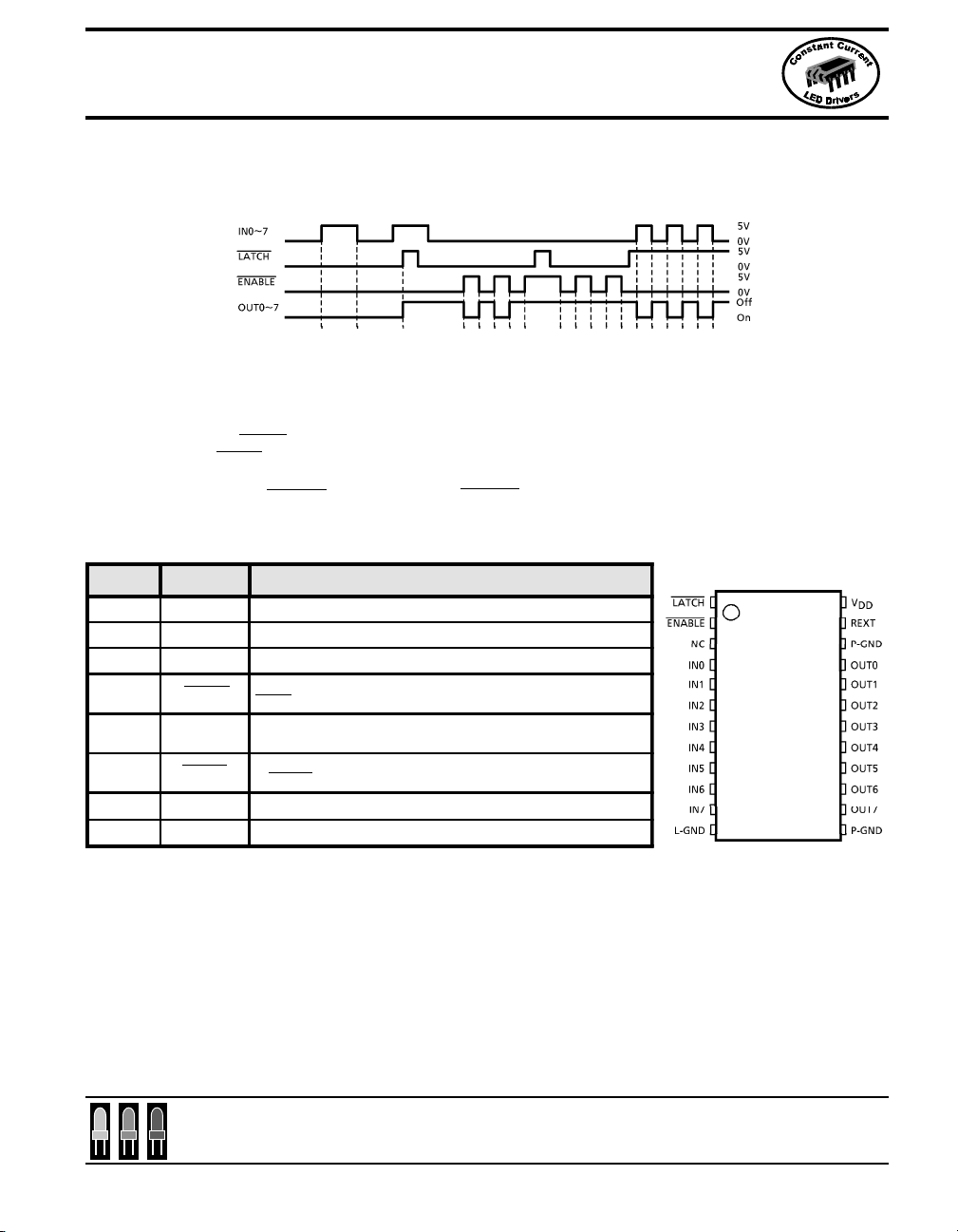
Timing Diagram:
Latches are:
1. Level Sesitive
2. Not edge sensitive
3. Not clock synchronous
4. Passing Data when LATCH is H
5. Hold Data when LATCH is L
All Outputs are OFF when ENABLE is H and ON when ENABLE is L.
Terminal Description & Pin Out:
PIN No. PIN NAME FUNCTION
12 L-GND GND terminal for control logic.
13,2 2 P-GND GNt terminal fo r output c onstant c urrent dr ivers.
4~11 IN0~7 Iinput terminal of a parallel-data for latches.
1LATCH
14~21
OUT0~7 Output terminals.
Input terminal of a data strobe. Latches passes data with "H" level input of
LATC H-terminal, a nd hold da ta wi th "L" leve l input.
rr
ent Interfent Interf
r
ent Interf
rr
ent Interfent Interf
ace Driace Dri
ace Dri
ace Driace Dri
vv
v
vv
erer
er
erer
2ENABLE
23 R-EXT Input terminal of connects with a resister for to set up all output current.
24 VDD 5V Supply voltage terminal
marktech
optoelectronics
For up-to-date product info visit our web site at www.marktechopto.com All specifications subject to change.
Input termi nal o f output enable . All o utputs (OUT0~7 ) do off wi th "H" level i nput
of ENABLE-terminal, and do on with "L" level input.
120 Broadway • Menands, New York 12204
Toll Free: (800) 98-4LEDS
• Fax: (518) 432-7454
567
TT
OSHIBOSHIB
T
OSHIB
TT
OSHIBOSHIB
A Bi-CMOSA Bi-CMOS
A Bi-CMOS
A Bi-CMOSA Bi-CMOS
Constant CurConstant Cur
Constant Cur
Constant CurConstant Cur
TB62707FTB62707F
TB62707F
TB62707FTB62707F
Truth Table:
IN0~7 LATCH ENABLE OUT 0~7
LL LOFF
HL LOFF
LH LOFF
HH LON
LLOFF
HLON
HHOFF
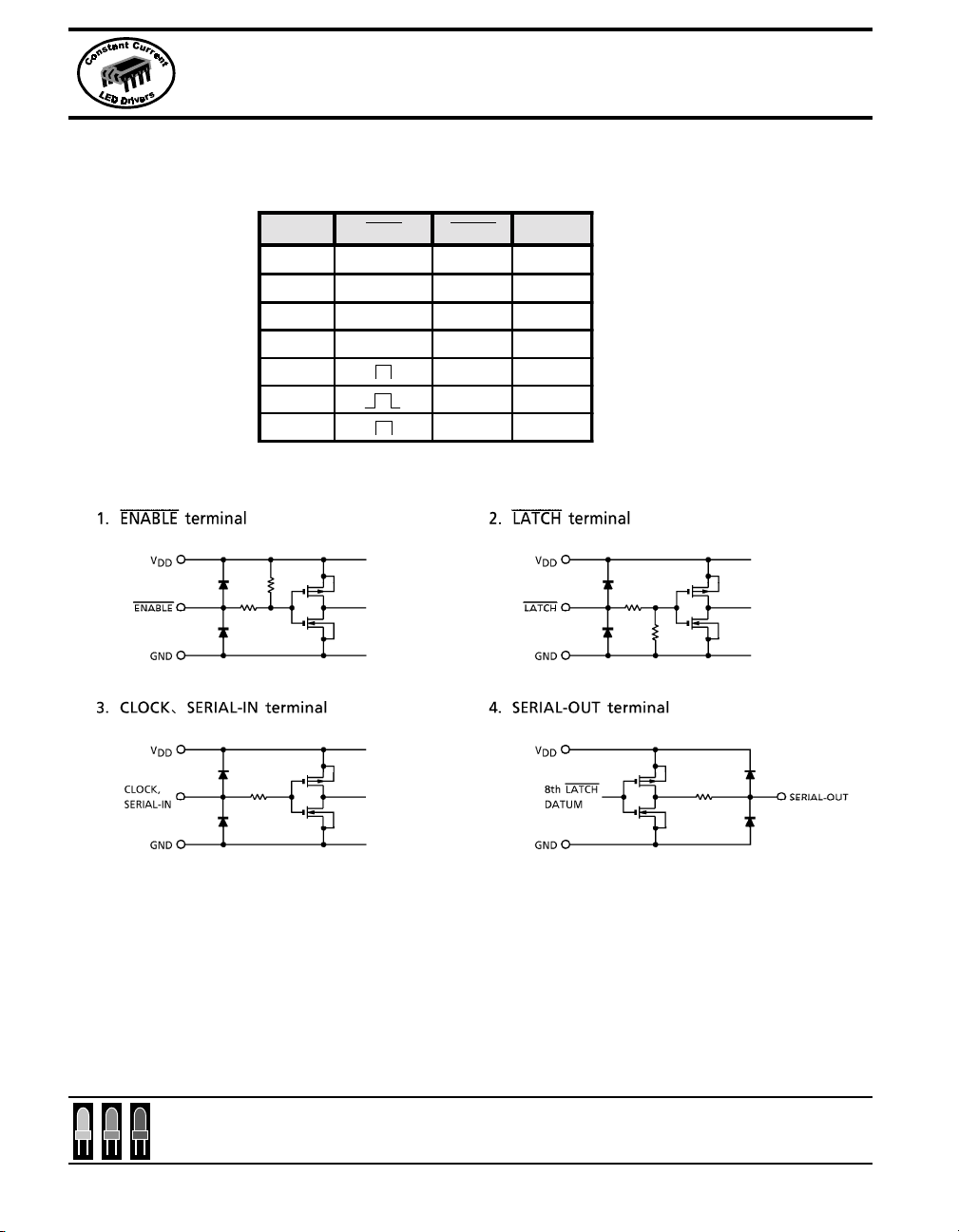
Equivalent Circuit of Inputs and Outputs:
rr
r
rr
ent Interfent Interf
ent Interf
ent Interfent Interf
ace Driace Dri
ace Dri
ace Driace Dri
vv
v
vv
erer
er
erer
marktech
optoelectronics
For up-to-date product info visit our web site at www.marktechopto.com All specifications subject to change.
568
Toll Free: (800) 98-4LEDS
120 Broadway • Menands, New York 12204
• Fax: (518) 432-7454

TT
OSHIBOSHIB
T
OSHIB
TT
OSHIBOSHIB
A Bi-CMOSA Bi-CMOS
A Bi-CMOS
A Bi-CMOSA Bi-CMOS
Constant CurConstant Cur
Constant Cur
Constant CurConstant Cur
TB62707FTB62707F
TB62707F
TB62707FTB62707F
Maximum Ratings:
CHARACTER SYMBOL RATING UNIT
Supply Voltage VDD +7.0 V
Output Voltage VOUT -0.5~+17.0 V
Outp ut C urrent IOUT +90 mA
Input Voltage VIN -0.3~VDD + 0.3 V
GND Terminal Current IGND 720 mA
Power Dissipation PD 0.78 W
Operating Temperature Topr -40~+85 °C
Storage Temperature Tstg -55~+150 °C
* On 50 x 50 x 1.66mm 30% Copper, Glass Epoxy PWB
Ambient Temperature Derated 6.66mW/ºC above 25ºC
Recommended Operating Condition:
rr
ent Interfent Interf
r
ent Interf
rr
ent Interfent Interf
ace Driace Dri
ace Dri
ace Driace Dri
vv
v
vv
erer
er
erer
CHARACTER SYMBOL CONDITION MIN . TYP. MAX. UNIT
Supply Voltage VDD 4.5 5.0 5.5 V
Output Voltage VOUT — — 15.0 V
IOUT DC 1 Circuit 5 — 88 mA
Output Current
Inp ut Vo l ta g e
LATCH Pulse Width
INP U T P uls e Wi dth
ENABLE Pulse Width
Set-up Time for LATCH tsetup(L) 100 — — ns
Hold Time for ENABLE thold(L) 100 — — ns
Power Dissipation P
marktech
optoelectronics
For up-to-date product info visit our web site at www.marktechopto.com All specifications subject to change.
IOH SERIAL-OUT — — -1.0 mA
IOL SE RIAL-OUT — — 1.0 mA
VIH 0.7VDD — VDD+0.3 V
VIL -0.3 — 0.3VDD V
tw LAT
tw IN 4500 — — ns
tw EN 4500 — — ns
D
VDD=4.5 ~ 5.5V
ON PCB ,Ta=85°C — — 0.6 W
Toll Free: (800) 98-4LEDS
100 — — ns
120 Broadway • Menands, New York 12204
• Fax: (518) 432-7454
569

TT
OSHIBOSHIB
T
OSHIB
TT
OSHIBOSHIB
A Bi-CMOSA Bi-CMOS
A Bi-CMOS
A Bi-CMOSA Bi-CMOS
Constant CurConstant Cur
Constant Cur
Constant CurConstant Cur
TB62707FTB62707F
TB62707F
TB62707FTB62707F
Electrical Characteristics:
CH ARAC TER ISTIC SYMBOL
Inp ut
Voltage
Output Leakage Current IOH — VOH=15.0V — — 10 µA
Output
Voltage
Output C urrent 1
Output C urrent 2
Supply Voltage
Regulation
Supply
Current
Reference Voltage Uref — — — 1.26 — V
"H" level VIH — — 0.7VDD — VD D
"L" level VIL — — GND — 0.3VDD
SERIAL--
OUT
Current
Skew
Current
Skew
"OFF"
"ON"
rr
ent Interfent Interf
r
ent Interf
rr
ent Interfent Interf
TEST
CIR-
CUIT
VOL — IOL=+1.0mA — — 0.4 V
VOH IOH=-1.0mA 4.6 — — V
IOL 1 — VC E= 0. 7V
IOL 2 — VC E =0 .4V 68 80 9 2
dIOL1 —
IOL 3 — VC E =0 .4V
IOL4 — VCE=0.7V 63.8 75.0 86.2
dIOL2 —
% / VDD — REXT=470Ω Ta=40~+85°C — 5 — % /V
IIDD (off) 1 — REXT=OPEN OUT~8=off — 0.6 1.2
IIDD (off) 2 — REXT=500 Ω OUT~8=off 6 8 10
IIDD (off) 3 — REXT=280 Ω OUT~8=off 12 15 18
IDD (on)1 — REXT=500Ω OUT~8=on 8 13 20
IDD (on)2 — REXT=280Ω OUT~8=on 18 25 35
CONDITION MIN. TYP. MAX. UNIT
REXT=620Ω
Matching)
IO= 40 mA ,
VCE=0.4V
IO= 75 mA ,
VCE=0.7V
REXT=620
REXT=330Ω
Matching)
REXT=330Ω
(include
Current
(Include
Current
Ω
ace Driace Dri
ace Dri
ace Driace Dri
35.7 42 48.3
— ±1.5 ±6.0 %
64.2 75.5 86.8
— ±1.5 ±5.0 %
vv
v
vv
erer
er
erer
V
mA
mA
mA
marktech
optoelectronics
For up-to-date product info visit our web site at www.marktechopto.com All specifications subject to change.
570
Toll Free: (800) 98-4LEDS
120 Broadway • Menands, New York 12204
• Fax: (518) 432-7454

TT
OSHIBOSHIB
T
OSHIB
TT
OSHIBOSHIB
A Bi-CMOSA Bi-CMOS
A Bi-CMOS
A Bi-CMOSA Bi-CMOS
Constant CurConstant Cur
Constant Cur
Constant CurConstant Cur
TB62707FTB62707F
TB62707F
TB62707FTB62707F
Switching Characteristics:
CHAR ACTE RIST IC SYMBOL
Propagation
Delay Time
("L" to "H")
Propagation
Delay Time
("H" to "L")
Pulse Width
Set-up Time for
Latch
Hold Time for
LATCH & CLOCK
Maximum CLOCK Rise Time tr — — — 10 µs
Maximum CLOCK Fall Time tf — — — 10 µs
Output Rise Time tor — 200 1000 120 0 ns
Output Fall Time to f — 200 100 0 120 0 ns
INn- OUT n
LATCH-OUTn — 600 1200 ns
ENABLE-OUTn — 600 1200 ns
INn- OUT n
LATCH-OUTn — 300 1200 ns
ENABLE-OUTn — 300 1200 ns
/ENABLE tw ENA — — 2000 3500 ns
/LATCH tw LAT — — 25 5 0 ns
/IN tw IN — — 2000 3500 ns
L-H
H-L — — 25 50 ns
L-H
H-L — — 0 15 ns
rr
r
rr
tpLH —
tpHL —
tsetup LAT
thold LAT
ent Interfent Interf
ent Interf
ent Interfent Interf
TEST
CIRCUIT
— — 25 50 ns
——015ns
CONDITION MIN. TYP. MAX. UNIT
VDD = 5.0V
VCE = 0.4V
REXT = 470Ω
IOUT = 40mA
CL = 10.5pF
VIH = VDD
VIL = GND
VL = 3.0V
RL = 65Ω
ace Driace Dri
ace Dri
ace Driace Dri
— 600 1200 ns
— 300 1200 ns
vv
v
vv
erer
er
erer
DC Characteristic Test Circuit: AC Characteristic Test Circuit:
marktech
optoelectronics
For up-to-date product info visit our web site at www.marktechopto.com All specifications subject to change.
Toll Free: (800) 98-4LEDS
120 Broadway • Menands, New York 12204
• Fax: (518) 432-7454
571

TT
OSHIBOSHIB
T
OSHIB
TT
OSHIBOSHIB
A Bi-CMOSA Bi-CMOS
A Bi-CMOS
A Bi-CMOSA Bi-CMOS
Constant CurConstant Cur
Constant Cur
Constant CurConstant Cur
TB62707FTB62707F
TB62707F
TB62707FTB62707F
Timing Wave Form:
rr
ent Interfent Interf
r
ent Interf
rr
ent Interfent Interf
ace Driace Dri
ace Dri
ace Driace Dri
vv
v
vv
erer
er
erer
marktech
optoelectronics
For up-to-date product info visit our web site at www.marktechopto.com All specifications subject to change.
572
Toll Free: (800) 98-4LEDS
120 Broadway • Menands, New York 12204
• Fax: (518) 432-7454

TT
OSHIBOSHIB
T
OSHIB
TT
OSHIBOSHIB
A Bi-CMOSA Bi-CMOS
A Bi-CMOS
A Bi-CMOSA Bi-CMOS
Constant CurConstant Cur
Constant Cur
Constant CurConstant Cur
TB62707FTB62707F
TB62707F
TB62707FTB62707F
Graphs:
rr
ent Interfent Interf
r
ent Interf
rr
ent Interfent Interf
ace Driace Dri
ace Dri
ace Driace Dri
vv
v
vv
erer
er
erer
marktech
optoelectronics
For up-to-date product info visit our web site at www.marktechopto.com All specifications subject to change.
Toll Free: (800) 98-4LEDS
120 Broadway • Menands, New York 12204
• Fax: (518) 432-7454
573

TT
OSHIBOSHIB
T
OSHIB
TT
OSHIBOSHIB
A Bi-CMOSA Bi-CMOS
A Bi-CMOS
A Bi-CMOSA Bi-CMOS
Constant CurConstant Cur
Constant Cur
Constant CurConstant Cur
TB62707FTB62707F
TB62707F
TB62707FTB62707F
Application Circuit:
Outline Drawing:
rr
ent Interfent Interf
r
ent Interf
rr
ent Interfent Interf
ace Driace Dri
ace Dri
ace Driace Dri
V
LED
Only necessary to reduce power dissipation (if required)
= VCE(tr V
vv
erer
v
er
vv
erer
) + Vf(LED) + VO(IC Supply)
SAT
marktech
optoelectronics
For up-to-date product info visit our web site at www.marktechopto.com All specifications subject to change.
574
Toll Free: (800) 98-4LEDS
120 Broadway • Menands, New York 12204
• Fax: (518) 432-7454
 Loading...