

TT
OSHIBOSHIB
T
OSHIB
TT
OSHIBOSHIB
A Bi-CMOSA Bi-CMOS
A Bi-CMOS
A Bi-CMOSA Bi-CMOS
Constant CurConstant Cur
Constant Cur
Constant CurConstant Cur
rr
ent Interfent Interf
r
ent Interf
rr
ent Interfent Interf
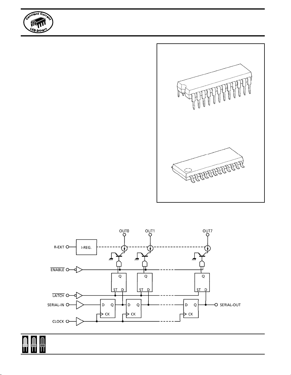
TB62706BN/BF
16 Bit Constant Current LED Driver with Shift
Register and Latch Functions
Product Description:
The TB62706BN/BF is specifically designed for
LED display applications. The Bi-CMOS device has
16 Bi-polar constant current output channels and
includes CMOS shift register and latch functions.
The LED drive current is programmed by the
installation of a single resistor per device. Current
is programmable from 5-90mA and is held constant
across all 16 outputs effectively compensating for
the inherent circuit and component variables which
affect the brightness of the LEDs.
Features:
• 16 Constant Current Output Channels
• Current Programmable from 5-90mA
• 5V CMOS Compatible Inputs
• 15MHz Max Clock Frequency (Cascade)
ace Driace Dri
ace Dri
ace Driace Dri
TB62706BN
SDIP24-P-300
TB62706BF
SSOP24-P-300B
vv
erer
v
er
vv
erer
Weight: 1.22g(typ)
Weight: 0.32g(typ)
Block Diagram:
marktech
optoelectronics
For up-to-date product info visit our web site at www.marktechopto.com All specifications subject to change.
556
Toll Free: (800) 98-4LEDS
120 Broadway • Menands, New York 12204
• Fax: (518) 432-7454
TT
OSHIBOSHIB
T
OSHIB
TT
OSHIBOSHIB
A Bi-CMOSA Bi-CMOS
A Bi-CMOS
A Bi-CMOSA Bi-CMOS
Constant CurConstant Cur
Constant Cur
Constant CurConstant Cur
TB62706BN/BF
Timing Diagram:
Latches are:
1. Level Sesitive
2. Not edge sensitive
3. Not clock synchronous
4. Passing Data when LATCH is H
5. Hold Data when LATCH is L
rr
ent Interfent Interf
r
ent Interf
rr
ent Interfent Interf
ace Driace Dri
ace Dri
ace Driace Dri
vv
v
vv
erer
er
erer
All Outputs are OFF when ENABLE is H and ON when ENABLE is L.
Terminal Description & Pin Out:
PIN No. PIN NAME FUNCTION
1 GND GND term inal for control lo gic .
2 SERIAL-IN Input terminal of a serial-data for shift-register
3 CLOCK Iinput terminal of a clock for data shift to up-edge.
4LATCH
5~20
21 ENABLE
22 SERIAL-OUT Output terminal of a serial-data for next SERIAL-IN terminal.
23 R-EX T Input terminal o f connects with a re sis ter for to set up al l output current.
24 VDD 5V Supply voltage terminal
OUT0~15 Output termi nals
marktech
optoelectronics
For up-to-date product info visit our web site at www.marktechopto.com All specifications subject to change.
Input terminal of a data strobe. Latches passes data with "H" level input of
LATCH-terminal, and hold data with "L" level input.
Input terminal of output enable. All outputs (OUT~15) do off with "H" level input
of ENABLE-terminal, and do on with "L" level input.
120 Broadway • Menands, New York 12204
Toll Free: (800) 98-4LEDS
• Fax: (518) 432-7454
557
TT
OSHIBOSHIB
T
OSHIB
TT
OSHIBOSHIB
A Bi-CMOSA Bi-CMOS
A Bi-CMOS
A Bi-CMOSA Bi-CMOS
Constant CurConstant Cur
Constant Cur
Constant CurConstant Cur
rr
r
rr
TB62706BN/BF
Truth Table:
CLOCK LATCH ENABLE S ERIAL-IN OUT0 OUT5 OUT7 SERIAL -OUT
UP H L Dn Dn Dn-7 Dn-15 Dn-15
UP L L Dn+1 No Change Dn-14
UP H L Dn+2 Dn+2 Dn-5 Dn-13 Dn-13
DOWN X L Dn+3 Dn+2 Dn-5 Dn-13 Dn-13
DOWN X H DN+3 Off Dn-13
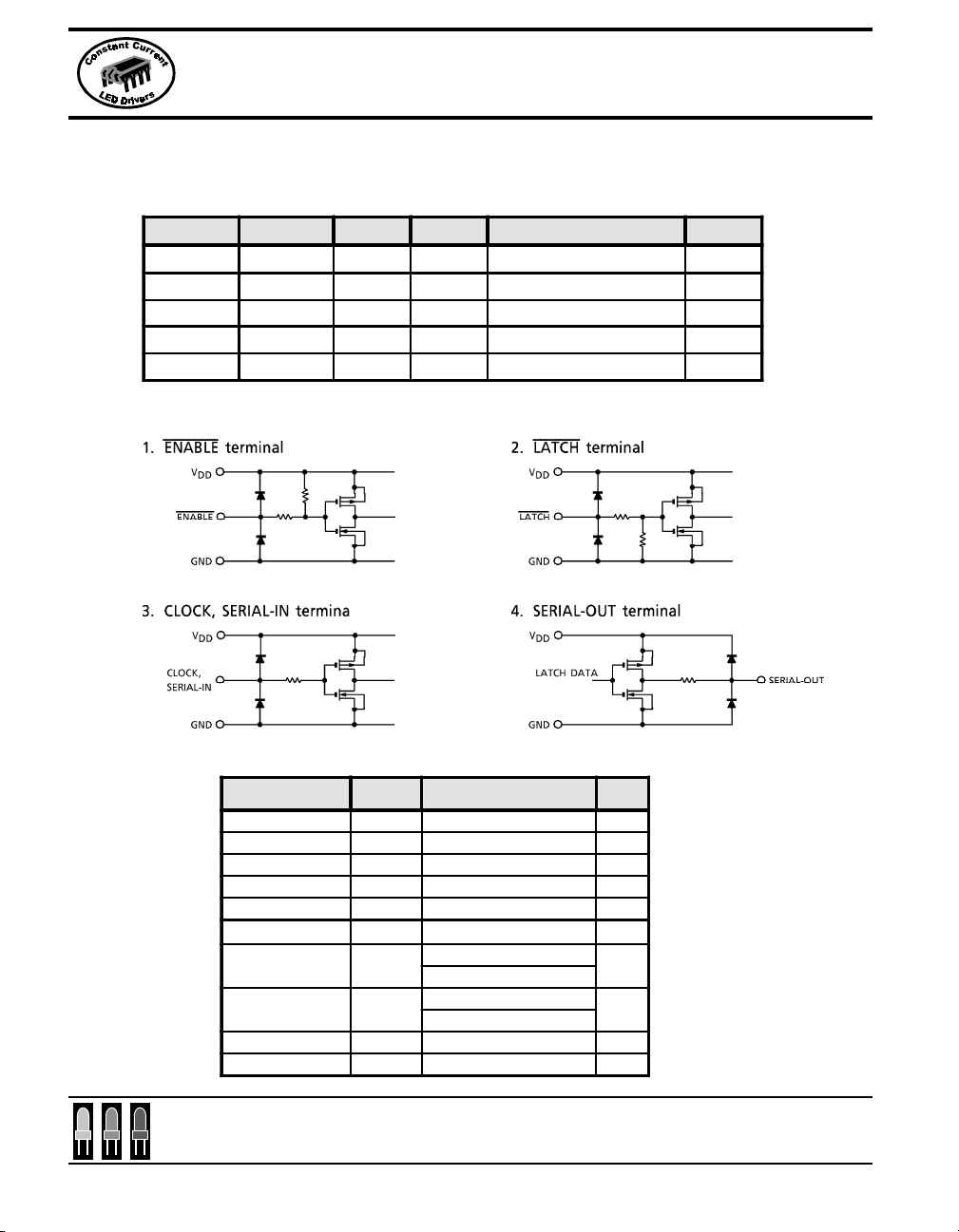
Equivalent Circuit of Inputs and Outputs:
ent Interfent Interf
ent Interf
ent Interfent Interf
ace Driace Dri
ace Dri
ace Driace Dri
vv
v
vv
erer
er
erer
Maximum Ratings:
CHARACTER SYMBOL RATING UNIT
Supply Voltage VDD 0~7.0 V
Input Voltage VIN -0.4~VDD + 0.4 V
Output Cu rrent IOUT +90 mA
Output Voltage VOUT -0.5~+17.0 V
Clock Frequency FCLK 15 MHz
GND Terminal Current IGND 1440 mA
Power Dissipation PD
Thermal Resistance Rth(j-a)
Operating Temperature Topr -40~+85 °C
Storage Temperature Tstg -55~+150 °C
marktech
optoelectronics
For up-to-date product info visit our web site at www.marktechopto.com All specifications subject to change.
558
1.78 (BN type: ON PCB,Ta=25°C)
1.00 (BF type: ON PCB,Ta=25°C)
70 (BN type: On PCB)
120 (BF type: On PCB)
120 Broadway • Menands, New York 12204
Toll Free: (800) 98-4LEDS
W
°C/W
• Fax: (518) 432-7454

TT
OSHIBOSHIB
T
OSHIB
TT
OSHIBOSHIB
A Bi-CMOSA Bi-CMOS
A Bi-CMOS
A Bi-CMOSA Bi-CMOS
Constant CurConstant Cur
Constant Cur
Constant CurConstant Cur
TB62706BN/BF
Recommended Operating Condition:
CHARACTERISTIC SYMBOL CONDITION MIN. TYP. MAX. UNIT
Supply Voltage VDD — 4.5 5.0 5.5 V
Outout Voltage VOUT — — — 15.0 V
IOUT DC 1 Circuit 5 — 88 mA
Output Current
Input Voltage
LATCH Pulse Width tw LAT
CLOCK Pulse Width tw CLK 50 — — ns
ENABLE Pulse Width tw EN 4500 — — ns
Set-up Time for DATA tsetup(D) 60 — — ns
Hold Time for Data thold(D) 20 — — ns
Set-up Time for LATCH tsetup(L) 100 — — ns
Hold Time for ENABLE thold(L) 60 — — ns
Clock Frequency FCLK Cascade Operation — — 10.0 MHz
Power Dissipation PD
IOH S E RIA L- OUT — — 1 .0 mA
IOL S ER IAL -O UT — — -1 .0 m A
VIH — 0.7VDD — VDD+0.3
VIL — -0.3 — 0.3VD D
rr
ent Interfent Interf
r
ent Interf
rr
ent Interfent Interf
VDD=4.5 ~ 5.5V
Ta=85°C (BN type) — — 0.92
Ta=85°C (BF type) — — 0.50
ace Driace Dri
ace Dri
ace Driace Dri
100 — — ns
vv
v
vv
erer
er
erer
V
W
marktech
optoelectronics
For up-to-date product info visit our web site at www.marktechopto.com All specifications subject to change.
Toll Free: (800) 98-4LEDS
120 Broadway • Menands, New York 12204
• Fax: (518) 432-7454
559

TT
OSHIBOSHIB
T
OSHIB
TT
OSHIBOSHIB
A Bi-CMOSA Bi-CMOS
A Bi-CMOS
A Bi-CMOSA Bi-CMOS
Constant CurConstant Cur
Constant Cur
Constant CurConstant Cur
TB62706BN/BF
Electrical Characteristics:
CH ARAC TE RISTIC SYMBOL
Inp ut
Voltage
Output Leakage Current IOH — VOH=15.0V — — 10 µA
Output
Voltage
Output Current 1
Output Current 2
Supply Voltage
Regulati on
Pull Up Resisto r RIN(up) — — 150 300 60 0 K Ω
Pull-down Resistor RIN(down) — — 1 00 200 4 00 KΩ
Supply
Current
"H" level VIH — Ta = -40~85ºC 0.7VDD — VDD
"L" level VIL — Ta = -40~85ºC GND — 0.3VDD
SERIAL--
OUT
Current
Skew
Current
Skew
"OFF"
"ON"
VOL — IOL=+1.0mA — — 0.4 V
VOH IOH=-1.0 mA 4 .6 — — V
IOL 1 — VC E =0. 7V
IOL2 — VCE=0.4V 33.7 3 9.5 45.3
dIOL1 —
IOL 3 — V CE =0 .7V
IOL4 — VCE=0.4V 63.8 7 5.0 86.2
dIOL2 —
% / VDD — REXT=470
IIDD (off) 1 — REXT=OPEN OUT~8=off — 0.6 1.2
IIDD (off) 2 — REXT=470Ω OUT~8=off 3.5 5.8 8
IIDD (off) 3 — REXT=250Ω OUT~8=off 6.5 10.2 15
IDD (on)1 — REXT=470Ω OUT~8=on 10 16 22
IDD (on)2 — REXT=250Ω OUT~8=on 18 28.3 38.5
TEST
CIR-
CUIT
rr
ent Interfent Interf
r
ent Interf
rr
ent Interfent Interf
CONDITION MIN. TYP. MAX. UNIT
REXT=470Ω
(include Current
IO= 40 mA ,
VCE=0.4V
IO= 75 mA ,
VCE=0.7V
REXT=470Ω
REXT=250Ω
(Include Current
REXT=250Ω
Ω
Ta = -40 ~+85°C — ±1.5 ±5 .0 % /V
Matching)
Matching)
ace Driace Dri
ace Dri
ace Driace Dri
34.1 40.0 45.9
— ±1.5 ±6.0 %
64.2 75.5 86.8
vv
v
vv
1.5 6.0 %
erer
er
erer
V
mA
mA
mA
marktech
optoelectronics
For up-to-date product info visit our web site at www.marktechopto.com All specifications subject to change.
560
Toll Free: (800) 98-4LEDS
120 Broadway • Menands, New York 12204
• Fax: (518) 432-7454

TT
OSHIBOSHIB
T
OSHIB
TT
OSHIBOSHIB
A Bi-CMOSA Bi-CMOS
A Bi-CMOS
A Bi-CMOSA Bi-CMOS
Constant CurConstant Cur
Constant Cur
Constant CurConstant Cur
TB62706BN/BF
Switching Characteristics:
CH ARAC TE RIS TIC SYMBOL
CLK-OUTn
Propagation
Delay Time
("L" to "H")
Propagation
Delay Time
("H" to "L")
Pulse Width
Set-up Time for
Latch
Hold Time for
LATCH
Maximum CLOCK Rise Time tr — — — 10 µs
Maximum CLOCK Fall Time tf — — — 10 µs
Output Rise Time tor — 150 300 600 ns
Output Fall Ti me tof — 150 300 600 ns
LATCH-OUTn — 1200 1500 ns
ENABLE-OUTn — 1200 1500 ns
CLK-SOUT — 30 70 ns
CLK-OUTn
LATCH-OUTn — 700 1000 ns
ENABLE-OUTn — 700 1000 ns
CLK-SOUT — 30 70 ns
CLK tw CLK,CLK — — 20 30 ns
LATCH tw LAT,LAT — — 10 25 ns
L-H
H-L — — 25 50 ns
L-H
H-L — — 0 15 ns
rr
r
rr
tpLH —
tpHL —
tsetup LAT
thold LAT
ent Interfent Interf
ent Interf
ent Interfent Interf
TEST
CIRCUIT
— — 25 50 ns
——015ns
ace Driace Dri
ace Dri
ace Driace Dri
CONDITION MIN. TYP. MAX. UNIT
VDD = 5.0V
VCE = 0.4V
VIH = VDD
VIL = GND
REXT = 470Ω
VL = 3.0V
RL = 65 Ω
CL = 10.5pF
vv
erer
v
er
vv
erer
— 1200 1500 ns
— 700 1000 ns
DC Characteristic Test Circuit: AC Characteristic Test Circuit:
marktech
optoelectronics
For up-to-date product info visit our web site at www.marktechopto.com All specifications subject to change.
Toll Free: (800) 98-4LEDS
120 Broadway • Menands, New York 12204
• Fax: (518) 432-7454
561

TT
OSHIBOSHIB
T
OSHIB
TT
OSHIBOSHIB
A Bi-CMOSA Bi-CMOS
A Bi-CMOS
A Bi-CMOSA Bi-CMOS
Constant CurConstant Cur
Constant Cur
Constant CurConstant Cur
TB62706BN/BF
Timing Wave Form:
rr
ent Interfent Interf
r
ent Interf
rr
ent Interfent Interf
ace Driace Dri
ace Dri
ace Driace Dri
vv
v
vv
erer
er
erer
marktech
optoelectronics
For up-to-date product info visit our web site at www.marktechopto.com All specifications subject to change.
562
Toll Free: (800) 98-4LEDS
120 Broadway • Menands, New York 12204
• Fax: (518) 432-7454

TT
OSHIBOSHIB
T
OSHIB
TT
OSHIBOSHIB
A Bi-CMOSA Bi-CMOS
A Bi-CMOS
A Bi-CMOSA Bi-CMOS
Constant CurConstant Cur
Constant Cur
Constant CurConstant Cur
TB62706BN/BF
Graphs:
rr
ent Interfent Interf
r
ent Interf
rr
ent Interfent Interf
ace Driace Dri
ace Dri
ace Driace Dri
vv
v
vv
erer
er
erer
marktech
optoelectronics
For up-to-date product info visit our web site at www.marktechopto.com All specifications subject to change.
Toll Free: (800) 98-4LEDS
120 Broadway • Menands, New York 12204
• Fax: (518) 432-7454
563

TT
OSHIBOSHIB
T
OSHIB
TT
OSHIBOSHIB
A Bi-CMOSA Bi-CMOS
A Bi-CMOS
A Bi-CMOSA Bi-CMOS
Constant CurConstant Cur
Constant Cur
Constant CurConstant Cur
rr
r
rr
TB62706BN/BF
Graphs:
Current Programming Resistor Selection:
ent Interfent Interf
ent Interf
ent Interfent Interf
ace Driace Dri
ace Dri
ace Driace Dri
vv
v
vv
erer
er
erer
marktech
optoelectronics
For up-to-date product info visit our web site at www.marktechopto.com All specifications subject to change.
564
Toll Free: (800) 98-4LEDS
120 Broadway • Menands, New York 12204
• Fax: (518) 432-7454

TT
OSHIBOSHIB
T
OSHIB
TT
OSHIBOSHIB
A Bi-CMOSA Bi-CMOS
A Bi-CMOS
A Bi-CMOSA Bi-CMOS
Constant CurConstant Cur
Constant Cur
Constant CurConstant Cur
TB62706BN/BF
Outline Drawings:
rr
ent Interfent Interf
r
ent Interf
rr
ent Interfent Interf
ace Driace Dri
ace Dri
ace Driace Dri
vv
v
vv
erer
er
erer
marktech
optoelectronics
For up-to-date product info visit our web site at www.marktechopto.com All specifications subject to change.
Toll Free: (800) 98-4LEDS
120 Broadway • Menands, New York 12204
• Fax: (518) 432-7454
565
 Loading...