

TT
OSHIBOSHIB
T
OSHIB
TT
OSHIBOSHIB
A Bi-CMOSA Bi-CMOS
A Bi-CMOS
A Bi-CMOSA Bi-CMOS
Constant CurConstant Cur
Constant Cur
Constant CurConstant Cur
rr
ent Interfent Interf
r
ent Interf
rr
ent Interfent Interf
ace Driace Dri
ace Dri
ace Driace Dri
vv
v
vv
erer
er
erer
TB62701AN
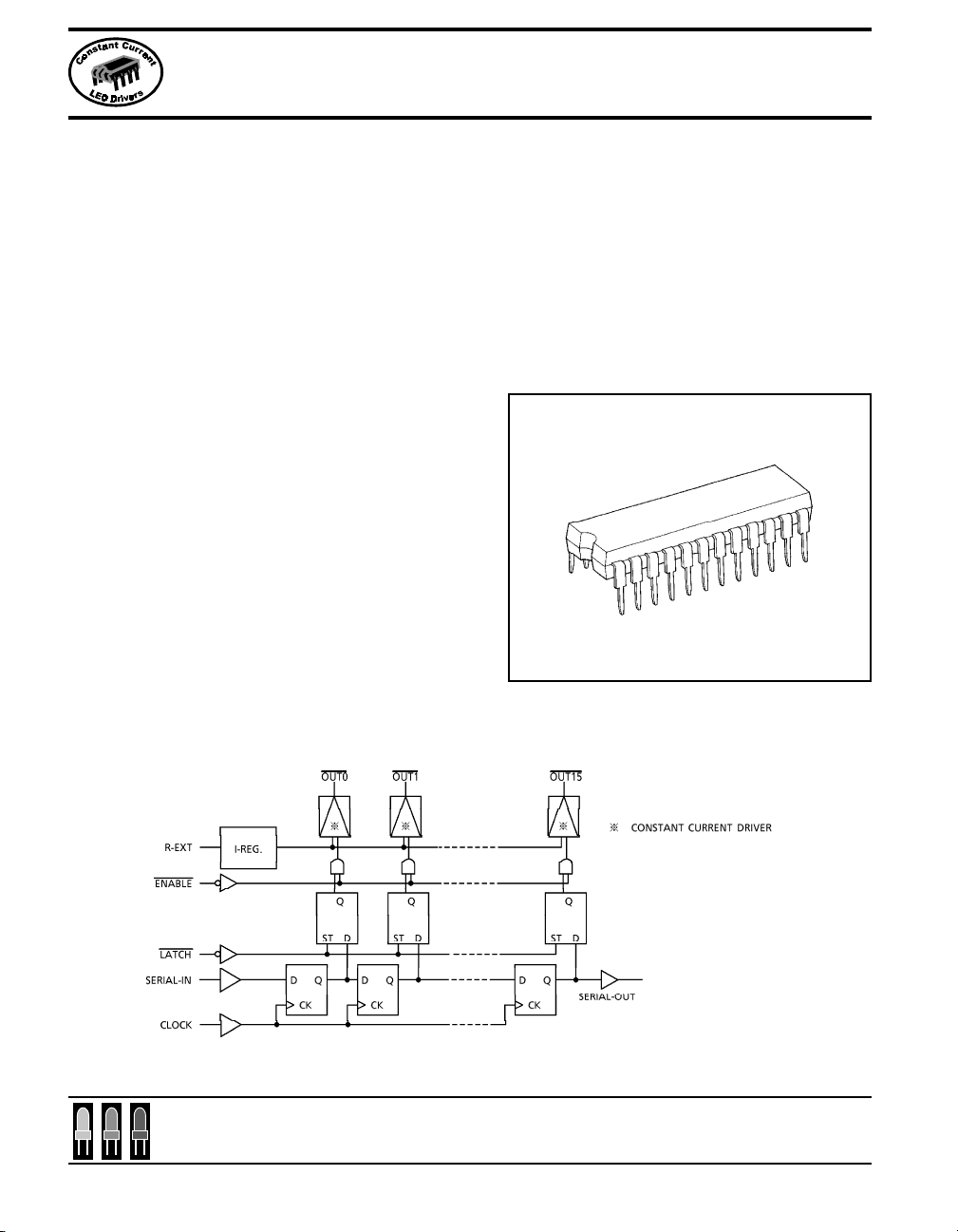
16 Bit Constant Current LED Driver with Shift Register and Latch Functions
Product Description:
The TB62701AN is specifically designed for LED display applications. The Bi-CMOS device has
16 Bi-polar constant current output channels and includes CMOS shift register and latch functions.
The LED drive current is programmed by the
installation of a single resistor per device.
Current is programmable from 5-50mA and is
held constant across all 16 outputs effectively
compensating for the inherent circuit and
component variables which affect the brightness of the LEDs.
Features:
• 16 Constant Current Output Channels
• Current Programmable from 5-50mA
• 5V CMOS Compatible Inputs
• Supports up to a 30V LED Supply Voltage
TB62701AN
SDIP24-P-300
Weight: 1.2g(typ)
Block Diagram:
marktech
optoelectronics
For up-to-date product info visit our web site at www.marktechopto.com All specifications subject to change.
536
Toll Free: (800) 98-4LEDS
120 Broadway • Menands, New York 12204
• Fax: (518) 432-7454
TT
OSHIBOSHIB
T
OSHIB
TT
OSHIBOSHIB
A Bi-CMOSA Bi-CMOS
A Bi-CMOS
A Bi-CMOSA Bi-CMOS
Constant CurConstant Cur
Constant Cur
Constant CurConstant Cur
TB62701ANTB62701AN
TB62701AN
TB62701ANTB62701AN
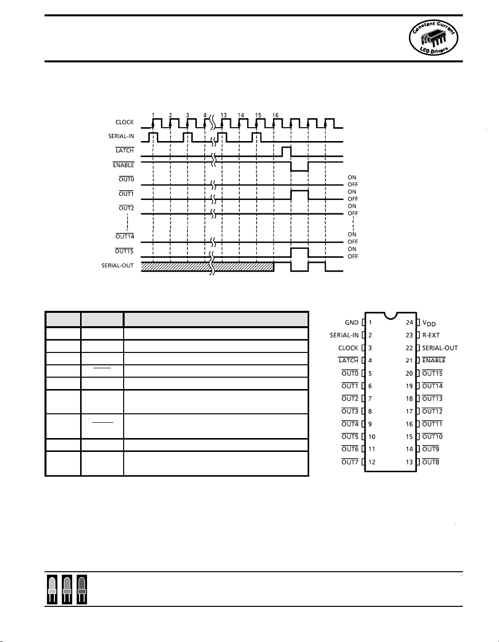
Timing Diagram:
Terminal Description & Pin Out:
PIN No. PIN NAME FUNCTION
1 GND GND terminal for control logic driver
2 SERIAL-IN Serial data input terminal for shift register
3 CLOCK Clock input terminal for data shift to up-edge
4 LATCH "H" : data through, "L" : data hold
24 V
5~12
13~20
OUTn Output terminals
DD
Supply voltage terminal
rr
ent Interfent Interf
r
ent Interf
rr
ent Interfent Interf
ace Driace Dri
ace Dri
ace Driace Dri
vv
v
vv
erer
er
erer
21 ENABLE
22 SERIAL-OUT Serial data output terminal for shift register
23 R-EXT
marktech
optoelectronics
For up-to-date product info visit our web site at www.marktechopto.com All specifications subject to change.
"H" output off, "L" : latch data = "H" then output on,
latch data = "L " then output off
The register which connects between R-EXT and GND sets the constant
output current.
120 Broadway • Menands, New York 12204
Toll Free: (800) 98-4LEDS
• Fax: (518) 432-7454
537
TT
OSHIBOSHIB
T
OSHIB
TT
OSHIBOSHIB
A Bi-CMOSA Bi-CMOS
A Bi-CMOS
A Bi-CMOSA Bi-CMOS
Constant CurConstant Cur
Constant Cur
Constant CurConstant Cur
TB62701ANTB62701AN
TB62701AN
TB62701ANTB62701AN
Truth Table:
INP UT OUTPUT OUTn (t = n)
CLOC K LATCH ENAB LE SE RIAL-IN OUT0 OUT7 OUT15 SERIAL-OUT
Up H L DN DN DN -7 DN-15 DN-15
Up L L DN No Change DN-15
Up
Down ∗∗DN No Change No Change
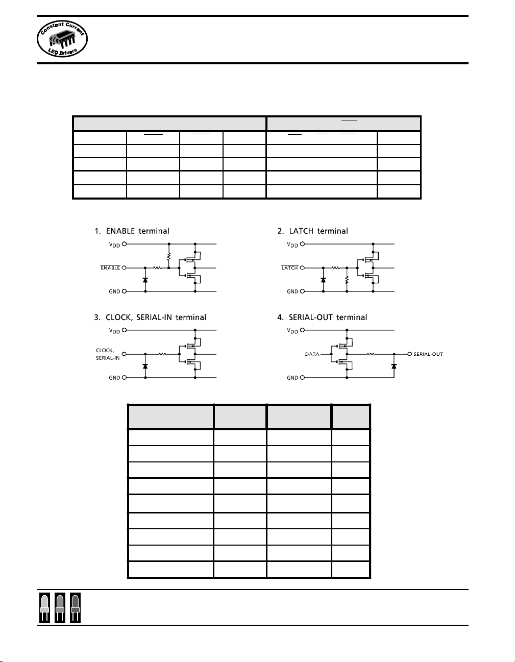
Equivalent Circuit of Inputs and Outputs:
∗
rr
r
rr
H DN OFF OFF OFF DN-15
ent Interfent Interf
ent Interf
ent Interfent Interf
ace Driace Dri
ace Dri
ace Driace Dri
vv
v
vv
erer
er
erer
Maximum Ratings:
CH ARACT ER SYMBOL RATING UNIT
Supp ly Volta ge VD D 0~+7.0 V
Output Voltag e V OUT -0.5~+30 V
Output Current IOUT 50 mA
Input Voltage VIN -0.4~VDD + 0.4 V
GND Terminal Current IGND 800 mA
Clock Frequency FCLK 2.5 MHz
Power Dissipation PD 1.78 W
Operating Temperature Topr -40~+85 °C
Storage Temperature Tstg -55~+150 °C
marktech
optoelectronics
For up-to-date product info visit our web site at www.marktechopto.com All specifications subject to change.
538
Toll Free: (800) 98-4LEDS
120 Broadway • Menands, New York 12204
• Fax: (518) 432-7454

TT
OSHIBOSHIB
T
OSHIB
TT
OSHIBOSHIB
A Bi-CMOSA Bi-CMOS
A Bi-CMOS
A Bi-CMOSA Bi-CMOS
Constant CurConstant Cur
Constant Cur
Constant CurConstant Cur
TB62701ANTB62701AN
TB62701AN
TB62701ANTB62701AN
Recommended Operating Condition
CHARACTERISTIC SYMBOL TES T C ONDITION MIN. TYP. MAX. UNIT
Supply Voltage VDD — 4.5 5.0 5.5 V
Output Voltage VOUT — — — 30.0 V
OUTn IOUT DC 1 circuit — — 45
Output Current
S-OUT
Inp ut Vo l t a g e V IN — 0 — V DD V
Data Set Up Time tsetup(D) — 100 — — ns
Data Hold Time thold (D) — 20 — — ns
Latch Set Up Time tsetup(L) — 300 — — ns
Latch Hold Time thold (L) — 100 — — ns
IOH — — — - 1. 0
IOL — — — 1 .0
rr
ent Interfent Interf
r
ent Interf
rr
ent Interfent Interf
ace Driace Dri
ace Dri
ace Driace Dri
vv
v
vv
erer
er
erer
mA
Clock Pulse Width
Latch Pulse Width
Clock Frequency fCK Cascade operation — 2.0 MHz
Power Dissipation PD Ta=85°C — 0.72 W
marktech
optoelectronics
For up-to-date product info visit our web site at www.marktechopto.com All specifications subject to change.
tw CLK — 100 — — ns
tw CLK — 100 — ns
tw LAT — 300 — ns
tw LAT — 300 — ns
120 Broadway • Menands, New York 12204
Toll Free: (800) 98-4LEDS
• Fax: (518) 432-7454
539

TT
OSHIBOSHIB
T
OSHIB
TT
OSHIBOSHIB
A Bi-CMOSA Bi-CMOS
A Bi-CMOS
A Bi-CMOSA Bi-CMOS
Constant CurConstant Cur
Constant Cur
Constant CurConstant Cur
TB62701ANTB62701AN
TB62701AN
TB62701ANTB62701AN
Electrical Characteristics:
CHAR ACTERIS TIC SYMBOL
Inp ut
Voltage
Output Leakage Current IOH — VOH=30V — — 10 µA
Output
Voltage
Output Current 1
Supp ly Volta ge
Regulation
Reference Volta ge Vref — REX T=56 0Ω, Ta =−40∼85°C — 1.26 — V
Pull Up / Down Resi stor RIN — — 100 200 400 kΩ
Supply
Current
"H" level VIH — — 70%VDD — VDD
"L" level VIL — — GND — 30%VDD
S-OUT
Delta
IOU T
"OFF"
"ON" IDD (on) — REXT=560Ω, OUTn=Off — 13.5 20 .0
VOL — IOL=+1.0mA — — 0.4
VOH — IOH=-1.0mA 4.6 — —
IOL 1 — V C E= 0. 7V
IOL2 — VCE=0.4V 33.1 39.0 44.9 mA
∆IOL 1
% / VDD — REXT=560
IIDD (o ff) 1 — RE XT=OPE N, OUTn=Off — 0.4 0.6
IID D ( o ff ) 2 — RE X T= 5 6 0 Ω, OUTn=Off — 6.5 10 .0
rr
ent Interfent Interf
r
ent Interf
rr
ent Interfent Interf
TEST
CIR-
CUIT
REX T=56 0Ω
—
IOUT=40mA,VCE=0.4V
ace Driace Dri
ace Dri
ace Driace Dri
TES T CONDIT ION MIN . TYP. MAX. UNIT
REX T=56 0
Ω
(include
∆IOL 1)
Ω
35.2 41.5 47.7 mA
— ±3.0 ±7.0 %
—18—% /V
vv
v
vv
erer
er
erer
V
V
mA
marktech
optoelectronics
For up-to-date product info visit our web site at www.marktechopto.com All specifications subject to change.
540
Toll Free: (800) 98-4LEDS
120 Broadway • Menands, New York 12204
• Fax: (518) 432-7454

TT
OSHIBOSHIB
T
OSHIB
TT
OSHIBOSHIB
A Bi-CMOSA Bi-CMOS
A Bi-CMOS
A Bi-CMOSA Bi-CMOS
Constant CurConstant Cur
Constant Cur
Constant CurConstant Cur
TB62701ANTB62701AN
TB62701AN
TB62701ANTB62701AN
Switching Characteristics:
CH ARACTE RISTIC SYMBOL TES T C OND ITION MIN. TYP. MAX. UNIT
CK-S -OUT
Propagation
Delay Time
("L" to "H")
Propagation
Delay Time
("H" to " L" )
Maximum Clock Frequency fMAX(*1) 2.0 — 2.5 MHz
Minimum
Pulse
Width
Data Set Up Time tsetup (D) — 17 50
Data Hold Time thold (D) — -7 10
Latch Set Up
Ti me
Latch Hold
Ti me
Maximum Clock Rise Time tr — — 10
Maximum Clock Fall Time tf — — 10
Maximum Output Rise Time tor — 35 80 ns
Maximum Output Fall Time tof — 40 80 ns
CK-OUTn — 130 500
LATCH-OUTn — 130 500
EN-OUTn — 130 500
CK-S -OUT
CK-OUTn — 130 500
LATCH-OUTn — 130 500
EN-OUTn — 130 500
CLK tw CLK — 45 80
LATCH tw LAT — 10 50
LH
HL — 70 200
LH
HL — -70 50
t
PLH
t
PLH
tLATsetup
tLAThold
rr
ent Interfent Interf
r
ent Interf
rr
ent Interfent Interf
VDD = 5.0V
VCE = 1.0V
VIH = VDD
VIL = GND
fCK = 2MHz
REXT = 560Ω
IOUT = 30mA
ace Driace Dri
ace Dri
ace Driace Dri
— 95 500
— 95 720
— 70 200
— -70 50
vv
v
vv
erer
er
erer
ns
ns
ns
ns
ns
ns
µs
DC Characteristic Test Circuit: AC Characteristic Test Circuit:
marktech
optoelectronics
For up-to-date product info visit our web site at www.marktechopto.com All specifications subject to change.
Toll Free: (800) 98-4LEDS
120 Broadway • Menands, New York 12204
• Fax: (518) 432-7454
541

TT
OSHIBOSHIB
T
OSHIB
TT
OSHIBOSHIB
A Bi-CMOSA Bi-CMOS
A Bi-CMOS
A Bi-CMOSA Bi-CMOS
Constant CurConstant Cur
Constant Cur
Constant CurConstant Cur
TB62701ANTB62701AN
TB62701AN
TB62701ANTB62701AN
Timing Wave Form:
rr
ent Interfent Interf
r
ent Interf
rr
ent Interfent Interf
ace Driace Dri
ace Dri
ace Driace Dri
vv
v
vv
erer
er
erer
marktech
optoelectronics
For up-to-date product info visit our web site at www.marktechopto.com All specifications subject to change.
542
Toll Free: (800) 98-4LEDS
120 Broadway • Menands, New York 12204
• Fax: (518) 432-7454

TT
OSHIBOSHIB
T
OSHIB
TT
OSHIBOSHIB
A Bi-CMOSA Bi-CMOS
A Bi-CMOS
A Bi-CMOSA Bi-CMOS
Constant CurConstant Cur
Constant Cur
Constant CurConstant Cur
TB62701ANTB62701AN
TB62701AN
TB62701ANTB62701AN
Graphs:
rr
ent Interfent Interf
r
ent Interf
rr
ent Interfent Interf
ace Driace Dri
ace Dri
ace Driace Dri
vv
v
vv
erer
er
erer
marktech
optoelectronics
For up-to-date product info visit our web site at www.marktechopto.com All specifications subject to change.
Toll Free: (800) 98-4LEDS
120 Broadway • Menands, New York 12204
• Fax: (518) 432-7454
543

TT
OSHIBOSHIB
T
OSHIB
TT
OSHIBOSHIB
A Bi-CMOSA Bi-CMOS
A Bi-CMOS
A Bi-CMOSA Bi-CMOS
Constant CurConstant Cur
Constant Cur
Constant CurConstant Cur
TB62701ANTB62701AN
TB62701AN
TB62701ANTB62701AN
Application Circuit:
rr
ent Interfent Interf
r
ent Interf
rr
ent Interfent Interf
ace Driace Dri
ace Dri
ace Driace Dri
vv
v
vv
erer
er
erer
marktech
optoelectronics
For up-to-date product info visit our web site at www.marktechopto.com All specifications subject to change.
544
Toll Free: (800) 98-4LEDS
120 Broadway • Menands, New York 12204
• Fax: (518) 432-7454

TT
OSHIBOSHIB
T
OSHIB
TT
OSHIBOSHIB
A Bi-CMOSA Bi-CMOS
A Bi-CMOS
A Bi-CMOSA Bi-CMOS
Constant CurConstant Cur
Constant Cur
Constant CurConstant Cur
TB62701ANTB62701AN
TB62701AN
TB62701ANTB62701AN
Outline Drawing:
rr
ent Interfent Interf
r
ent Interf
rr
ent Interfent Interf
ace Driace Dri
ace Dri
ace Driace Dri
vv
v
vv
erer
er
erer
marktech
optoelectronics
For up-to-date product info visit our web site at www.marktechopto.com All specifications subject to change.
Toll Free: (800) 98-4LEDS
120 Broadway • Menands, New York 12204
• Fax: (518) 432-7454
545
 Loading...