

Page 1
Service
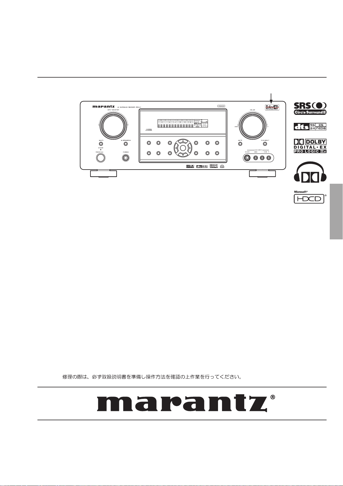
ZR6001
SURROUND
DISPLAY
PURE
SETUP
DIRECT
SIMPLE
AUTO
HT-EQ
MENU
ENTER
MEMORY
CLEAR
T-MODE
EXIT
BAND
MODE
OFF
ZR6001 /
N1B/N1S/
U1B
Manual
SECTION PAGE
1. TECHNICAL SPECIFICATIONS ........................................................................................... 1
2. TECHNICAL DESCRIPTION ............................................................................................... 3
3. POWER AMPLIFIER ADJUSTMENT .................................................................................. 8
4. SERVICE MODE ................................................................................................................. 8
5. SYSTEM ERROR ................................................................................................................10
6. UPDATE FIRMWARE .........................................................................................................11
[A] SOFTWARE (fdtv30300.exe) DOWNLOAD AND INSTALL PROCEDURE ..................11
[B] WRITING AND UPDATE SOFTWARE ......................................................................... 26
Mode 1 : Update DSP's software to 4M Flash-ROM .................................................... 27
Mode 2 : Update MAIN CPU's software to internal Flash-ROM ....................................31
Mode 3 : Update SUB CPU's software to internal Flash-ROM ..................................... 36
Mode 4 : Update PLC's firmware to PLC MODULE ...................................................... 46
7. WIRING DIAGRAM .............................................................................................................51
8. BLOCK DIAGRAM .............................................................................................................53
9. SCHEMATIC DIAGRAM .................................................................................................... 55
10. PARTS LOCATION .............................................................................................................75
11. IC DATA ...............................................................................................................................91
12. EXPLODED VIEW AND PARTS LIST ..............................................................................107
13. ELECTRICAL PARTS LIST ............................................................................................... 111
DISP MULTI AUTO TUNED ST V—OFF NIGHT PEAK ANALOG
SURR
SLEEP
AUTO DIRECT DISC 6.1 MTX 6.1 SPKR B EQ
SURROUND
PURE
SIMPLE
SETUP
DIRECT
MODE
AUTO
HT-EQ
MENU
ENTER
SURROUND
ATT
DIGITAL
DIGITAL
LCR
LFE
AAC
PCM
SL S SR
DISPLAY
MEMORY
EXIT
TABLE OF CONTENTS
AV Surround Receiver
/U Version only
CLEAR
T-MODE
BAND
Please use this ser
vice manual with referring to the user guide ( D.F.U. ) without fail.
ZR6001
Part no. 90M15CW855010
First Issue 2006.03
MZ
Page 2
MARANTZ DESIGN AND SERVICE
Using superior design and selected high grade components,
Only original
MARANTZ
parts can insure that your
MARANTZ
MARANTZ
product will continue to perform to the specifi cations for which
company has created the ultimate in stereo sound.
it is famous.
Parts for your
MARANTZ
ORDERING PARTS :
equipment are generally available to our National Marantz Subsidiary or Agent.
Parts can be ordered either by mail or by Fax.. In both cases, the correct part number has to be specifi ed.
The following information must be supplied to eliminate delays in processing your order :
1. Complete address
2. Complete part numbers and quantities required
3. Description of parts
4. Model number for which part is required
5. Way of shipment
6. Signature : any order form or Fax. must be signed, otherwise such part order will be considered as null and void.
USA
MARANTZ AMERICA, INC
1100 MAPLEWOOD DRIVE
ITASCA, IL. 60143
USA
PHONE : 630 - 741 - 0300
FAX : 630 - 741 - 0301
AUSTRALIA
QualiFi Pty Ltd,
24 LIONEL ROAD,
MT. WAVERLEY VIC 3149
AUSTRALIA
PHONE : +61 - (0)3 - 9543 - 1522
FAX : +61 - (0)3 - 9543 - 3677
EUROPE / TRADING
MARANTZ EUROPE B.V.
P. O. BOX 8744, BUILDING SILVERPOINT
BEEMDSTRAAT 11, 5653 MA EINDHOVEN
THE NETHERLANDS
PHONE : +31 - 40 - 2507844
FAX : +31 - 40 - 2507860
THAILAND
MRZ STANDARD CO., LTD
746 - 754 MAHACHAI ROAD.,
WANGBURAPAPIROM, PHRANAKORN,
BANGKOK, 10200 THAILAND
PHONE : +66 - 2 - 222 9181
FAX : +66 - 2 - 224 6795
CANADA
MARANTZ CANADA INC.
5-505 APPLE CREEK BLVD.
MARKHAM, ONTARIO L3R 5B1
CANADA
PHONE : 905 - 415 - 9292
FAX : 905 - 475 - 4159
SINGAPORE
WO KEE HONG DISTRIBUTION PTE LTD
No.1 JALAN KILANG TIMOR
#08-03 PACIFIC TECH CENTRE
SINGAPORE 159303
PHONE : +65 6376 0338
FAX : +65 6376 0166
NEW ZEALAND
WILDASH AUDIO SYSTEMS NZ
14 MALVERN ROAD MT ALBERT
AUCKLAND NEW ZEALAND
PHONE : +64-9-8451958
FAX :+64-9-8463554
JAPAN
D&M Holdings Inc.
D&M BUILDING, 2-1 NISSHIN-CHO,
KAWASAKI-KU, KAWASAKI-SHI,
KANAGAWA, 210-8569 JAPAN
TAIWAN
PAI- YUING CO., LTD.
6 TH FL NO, 148 SUNG KIANG ROAD,
TAIPEI, 10429, TAIWAN R.O.C.
PHONE : +886 - 2 - 25221304
FAX : +886 - 2 - 25630415
MALAYSIA
WO KEE HONG ELECTRONICS SDN. BHD.
2ND FLOOR BANGUNAN INFINITE CENTRE
LOT 1, JALAN 13/6, 46200 PETALING JAYA
SELANGOR DARUL EHSAN, MALAYSIA
PHONE : +60 - 3 - 7954 8088
FAX :+60-3-79547088
KOREA
MARANTZ KOREA CO., LTD.
ROOM 604, ELECTRO OFFICE, 16-58,
HANGGANG-RO 3GA, YONGSAN-KU,
SEOUL, 140-013, KOREA
PHONE : +82 - 2 - 323 - 2155
FAX : +82 - 2 - 323 - 2154
CHINA
MARANTZ SHANGHAI TRADING LTD.
ROOM.506 SHANGHAI LIGHT INDUSTRY MANSION
1578 NANJING (WEST) ROAD SHANGHAI
CHINA
TEL : 021 - 6248 - 1064
FAX : 021 - 6248 - 3565
SHOCK, FIRE HAZARD SERVICE TEST :
CAUTION : After servicing this appliance and prior to returning to customer, measure the resistance between either primary AC
cord connector pins ( with unit NOT connected to AC mains and its Power switch ON ), and the face or Front Panel of product and
controls and chassis bottom.
Any resistance measurement less than 1 Megohms should cause unit to be repaired or corrected before AC power is applied, and
verifi ed before it is return to the user/customer.
Ref. UL Standard No. 1492.
In case of diffi culties, do not hesitate to contact the Technical
Department at above mentioned address.
060223MZ
Page 3

TECHNICAL SPECIFICA TIONS
1.
FM TUNER SECTION
Frequency Range ....................................... 87.5 - 108.0 MHz
Usable Sensitivity .................................. IHF 1.8 µV/16.4 dBf
Signal to Noise Ratio ..........................Mono/Stereo 75/70 dB
Distortion ...........................................Mono/Stereo 0.2/0.3 %
Stereo Separation ............................................... 1 kHz 45 dB
Alternate Channel Selectivity ...................... ± 300 kHz 60 dB
Image Rejection ............................................... 98 MHz 70 dB
Tuner Output Level ..................1 kHz, ± 75 kHz Dev 800 mV
AM TUNER SECTION
Frequency Range ..................................531 - 1602 kHz [ /N ]
..................................520 - 1710 kHz [ /U ]
Signal to Noise Ratio .................................................... 50 dB
Usable Sensitivity .............................................. Loop 400 µV
Distortion ........................................ 400Hz, 30 % Mod. 0.5 %
Selectivity ......................................................± 18 kHz 70 dB
AUDIO SECTION
Power Output (20 Hz - 20 kHz/THD=0.08%)
Front L&R ............................................. 8 ohms 95 W / Ch
Center .................................................. 8 ohms 95 W / Ch
Surround L&R ...................................... 8 ohms 95 W / Ch
Surround Back L&R ............................. 8 ohms 95 W / Ch
GENERAL
Power Requirement ......................... AC 230 V 50/60 Hz [ /N ]
..............................AC 120 V 60 Hz [ /U ]
Power Consumption ............................................600 W [ /N ]
..................................................5A [ /U ]
Weight .......................................................13.7 kg (30.2 lbs)
ACCESSORIES
Remote Control Unit RC5500SR ..........................................1
AAA-size batteries ............................................................... 2
FM Antenna ..........................................................................1
AM Loop Antenna .................................................................1
Front AUX Jack Cover ......................................................... 1
AC Power Cable ...................................................................1
1 in.
(25 mm)
Front L&R ........................................... 6 ohms 115 W / Ch
Center ................................................ 6 ohms 115 W / Ch
Surround L&R .................................... 6 ohms 115 W / Ch
Surround Back L&R ........................... 6 ohms 115 W / Ch
Input Sensitivity/Impedance ...................... 168 mV/ 47 kohms
Signal to Noise Ratio
(Analog Input / Pure Direct) ................................. 105 dB
Frequency Response
(Analog Input / Pure Direct) ........ 8 Hz - 100 kHz (± 3 dB)
(Digital Input / 96 kHz PCM) ......... 8 Hz - 45 kHz (± 3 dB)
VIDEO SECTION
Television Format ..................................................NTSC/PAL
Input Level/Impedance ..................................1 Vp-p/75 ohms
Output Level/Impedance ................................1 Vp-p/75 ohms
Video Frequency Response .............. 5 Hz to 8 MHz (- 1 dB)
Video Frequency (Component) .......5 Hz to 80 MHz (- 1 dB)
S/N ................................................................................ 60 dB
PLC SECTION
Modulation Method .............................................. Multi carrier
Frequency Band ...........................................2 MHz - 20 MHz
INPUT SELECTOR
MULTI
STANDBY
POWER ON / STANDBY PHONES
17-5/16 ins. (440 mm)
AV SURROUND RECEIVER ZR6001
DISP MULTI AUTO TUNED ST V—OFF NIGHT PEAK ANALOG
SURR
SLEEP
AUTO DIRECT DISC 6.1 MT X 6.1 EQ
SURROUND
PURE
SIMPLE
MODE
SETUP
DIRECT
M. SPEAKER B
ENTER
AUTO
HT-EQ
MENU
(463 mm)
18-1/4 ins.
(418 mm)
16-1/2 ins.
(20 mm)
13/16 ins.
SURROUND
ATT
DIGITAL
DIGITAL
LCR
LFE
PCM
SL S SR
DISPLAY
MEMORY
EXIT
BAND
VOLUME
DOWN
UP
CLEAR
MUTE
T-MODE
7.1CH INPUT
AUX 1 INPUT
AUDIOS-VIDEO VIDEO L R
5-3/4 ins.
(146 mm)
(162 mm)
6-7/16 ins.
(16 mm)
11/16 ins.
1
Page 4

The relation between the selected surround mode and the input signal
The surround mode is selected with the surround mode buttons on ZR6001 or the remote control unit. However, the sound
you hear is subject to the relationship between the selected surround mode and input signal. That relationship is as follows;
Surround Mode Input Signal Decoding
AUTO Dolby Surr. EX Dolby Digital EX
PURE DIRECT Dolby D Surr. EX Dolby Digital EX
EX/ES Dolby D Surr. EX Dolby Digital EX
DOLBY Dolby D Surr. EX Dolby Digital 5.1
(PLIIx movie) Dolby D (5.1ch) Dolby Digital 5.1
(PLIIx music) Dolby D (2ch) Pro Logic IIx
(PLIIx game) Dolby D (2ch Surr) Pro Logic IIx
(Pro Logic) PCM (Audio) Pro Logic IIx
DTS DTS-ES DTS 5.1
(Neo:6 Cinema) DTS 96/24 DTS 96/24
(Neo:6 Music) DTS (5.1ch) DTS 5.1
II
Cinema PCM (Audio) CS
CS
CS
II
Music Analog CS
CS
II
Mono Dolby D (2ch) CS
STEREO Dolby Surr. EX Stereo
Virtual Dolby Surr. EX Virtual
Multi Ch. Dolby Surr. EX Dolby Digital EX
Stereo Dolby D (5.1ch) Dolby Digital 5.1
Dolby D (5.1ch) Dolby Digital 5.1
Dolby D(2ch) Dolby Digital 2.0
Dolby D (2ch Surr) Pro Logic IIx movie
DTS-ES DTS-ES
DTS 96/24 DTS 96/24
DTS (5.1ch) DTS 5.1
PCM(Audio) PCM (Stereo)
PCM 96kHz PCM (96kHz Stereo)O- - - - PCM L, R
Analog Stereo
Dolby D (5.1ch) Dolby Digital 5.1
Dolby D (2ch) Dolby Digital 2.0
Dolby D (2ch Surr) Pro Logic IIx movie
DTS-ES DTS-ES
DTS 96/24 DTS 96/24
DTS (5.1ch) DTS 5.1
PCM (Audio) PCM (Stereo)
PCM 96kHz PCM (96kHz Stereo)O- - - - PCM L, R
HDCD PCM (Stereo)
Analog Stereo
Dolby D (5.1ch) Dolby Digital EX
DTS-ES DTS-ES
DTS(5.1ch) DTS-ES
Analog Pro Logic IIx
PCM (Audio) Neo:6
Analog Neo:6
Dolby D (2ch) Neo:6
Dolby D (2ch Surr) Neo:6
Dolby D (2ch Surr) CS
Dolby D (5.1ch) Stereo
Dolby D (2ch) Stereo
Dolby D (2ch Surr) Stereo
DTS-ES Stereo
DTS 96/24 Stereo
DTS (5.1ch) Stereo
PCM (Audio) Stereo
PCM 96kHz Stereo
HDCD PCM (Stereo)
Analog Stereo
Dolby D (5.1ch) Virtual
Dolby D (2ch) Virtual
Dolby D (2ch Surr) Virtual
DTS-ES Virtual
DTS (5.1ch) Virtual
PCM (Audio) Virtual
Analog Virtual
Dolby D (2ch) Multi Channel Stereo
Dolby D (2ch Surr) Multi Channel Stereo
DTS-ES DTS-ES
DTS (5.1ch) DTS 5.1
PCM (Audio) Multi Channel Stereo
Analog Multi Channel Stereo
II
II
II
II
Output Channel Front information display
SL SBL
L/R C
OOOOO2 DIGITAL L, C, R, SL, SR, S, LFE
OOO-O2 DIGITAL L, C, R, SL, SR, LFE
O
-- --2 DIGITAL L, R
OOOO-2
OOOOO
OOO-O
OOO-O
O
- - - - PCM L, R
O
- - - - ANALOG OOOOO2 DIGITAL L, C, R, SL, SR, S, LFE
OOO-O2 DIGITAL L, C, R, SL, SR, LFE
O
-- --2 DIGITAL L, R
OOOO-2
OOOOO
OOO-O
OOO-O
O
- - - - PCM L, R
O
- - - - PCM HDCD L, R
O
- - - - ANALOG OOOOO2 DIGITAL L, C, R, SL, SR, S, LFE
OOOOO2 DIGITAL L, C, R, SL, SR, LFE
OOOOO
OOOOO
OOOOO2 DIGITAL L, C, R, SL, SR, S, LFE
OOOOO2 DIGITAL L, C, R, SL, SR, LFE
OOOO-2
OOOO-2
OOOO
OOOO
OOO-O
OOO-O
OOO-O
OOOO
OOOO
OOOO-2
OOOO-2
OOOOO
OOOOO
OOOOO2 DIGITAL L, R
OOOOO2 DIGITAL , 2 SURROUND L, R, S
O
-- -O2
O
-- -O2
O
-- --2 DIGITAL L, R
O
-- --2DIGITAL , 2 SURROUND L, R, S
O
-- -Odts, ES L, C, R, SL, SR, S, LFE
O
-- -Odts 96/24 L, C, R, SL, SR, LFE
O
-- -Odts L, C, R, SL, SR, LFE
O
- - - - PCM L, R
O
- - - - PCM L, R
O
- - - - PCM HDCD L, R
O
- - - - ANALOG O
-- --2 DIGITAL L, C, R, SL, SR, S, LFE
O
-- --2 DIGITAL L, C, R, SL, SR, LFE
O
-- --2 DIGITAL L, R
O
-- --2 DIGITAL , 2 SURROUND L, R, S
O
- - - - dts, ES L, C, R, SL, SR, S, LFE
O
- - - - dts L, C, R, SL, SR, LFE
O
- - - - PCM L, R
O
- - - - ANALOG OOOOO2 DIGITAL L, C, R, SL, SR, S, LFE
OOO-O2 DIGITAL L, C, R, SL, SR, LFE
OOOO-2
OOOO-2
OOOOO
OOO-O
OOOO
OOOO
SR SBR
SubW
Signal format indicators Channel status
DIGITAL , 2 SURROUND L, R, S
dts, ES L, C, R, SL, SR, S, LFE
dts 96/24 L, C, R, SL, SR, LFE
dts L, C, R, SL, SR, LFE
DIGITAL , 2 SURROUND L, R, S
dts, ES L, C, R, SL, SR, S, LFE
dts 96/24 L, C, R, SL, SR, LFE
dts L, C, R, SL, SR, LFE
dts , ES L, C, R, SL, SR, S, LFE
dts L, C, R, SL, SR, LFE
DIGITAL L, R
DIGITAL , 2 SURROUND L, R, S
- PCM L, R
- ANALOG dts, ES L, C, R, SL, SR, S, LFE
dts 96/24 L, C, R, SL, SR, LFE
dts L, C, R, SL, SR, LFE
- PCM L, R
- ANALOG -
DIGITAL L, R
DIGITAL , 2 SURROUND L, R, S
PCM L, R
ANALOG -
DIGITAL L, C, R, SL, SR, S, LFE
DIGITAL L, C, R, SL, SR, LFE
DIGITAL L, R
DIGITAL , 2 SURROUND L, R, S
dts, ES L, C, R, SL, SR, S, LFE
dts L, C, R, SL, SR, LFE
- PCM L, R
- ANALOG -
Notes:
• Dolby Digital (2 ch: Lt/Rt): signal with Dolby
Surround flag Speakers are full set.
• No sound outputs from the surround speaker,
center speaker and subwoofer if the DVD disc has
no surround data.
Abbreviations
L/R : Front speakers
C : Center speaker
SL/SR : Surround speakers
SBL/SBR : Surround Back speakers
SubW : Sub woofer speaker
2
Page 5

TECHNICAL DESCRIPTION
2.
DTS was introduced in 1994 to provide 5.1 channels
of discrete digital audio into home theater systems.
DTS brings you premium quality discrete
multichannel digital sound to both movies and music.
DTS is a multichannel sound system designed to
create full range digital sound reproduction.
The no compromise DTS digital process sets the
standard of quality for cinema sound by delivering
an exact copy of the studio master recordings to
neighborhood and home theaters.
Now, every moviegoer can hear the sound exactly
as the moviemaker intended.
DTS can be enjoyed in the home for either movies
or music on of DVD’s, LD’s, and CD’s.
“DTS” and “DTS Digital Surround” are registered
trademarks of Digital Theater Systems, Inc.
DTS-ES Extended Surround is a new multichannel
digital signal format developed by Digital Theater
Systems Inc. While offering high compatibility with
the conventional DTS Digital Surround format,
DTS-ES Extended Surround greatly improves the
360-degree surround impression and space
expression thanks to further expanded surround
signals. This format has been used professionally
in movie theaters since 1999.
In addition to the 5.1 surround channels (FL, FR, C,
SL, SR and LFE), DTS-ES Extended Surround
also offers the SB (Surround Back) channel for
surround playback with a total of 6.1 channels.
DTS-ES Extended Surround includes two signal
formats with different surround signal recording
methods, as DTS-ES Discrete 6.1 and DTS-ES
Matrix 6.1.
“DTS”, “DTS-ES” and “Neo:6” are trademarks of
Digital Theater Systems, Inc.
The advantages of discrete multichannel systems
over matrix are well known.
But even in homes equipped for discrete
multichannel, there remains a need for high-quality
matrix decoding. This is because of the large library
of matrix surround motion pictures available on disc
and on VHS tape; and analog television broadcasts.
The typical matrix decoder of today derives a
center channel and a mono surround channel from
two-channel matrix stereo material. It is better than
a simple matrix in that it includes steering logic to
improve separation, but because of its mono,
band-limited surround it can be disappointing to
users accustomed to discrete multichannel.
Neo:6 offers several important improvements as
follow,
• Neo:6 provides up to six full-band channels of
matrix decoding from stereo matrix material.
Users with 6.1 and 5.1 systems will derive six
and five separate channels, respectively,
corresponding to the standard home-theater
speaker layouts.
•
Neo:6 technology allows various sound elements
within a channel or channels to be steered
separately, and in a way which follows naturally
from the original presentation.
•
Neo:6 offers a music mode to expand stereo
nonmatrix recordings into the five- or six-channel
layout, in a way which does not diminish the subtlety
and integrity of the original stereo recording.
The stereo CD is a 16-bit medium with sampling at
44.1 kHz. Professional audio has been 20- or 24bit for some time, and there is increasing interest in
higher sampling rates both for recording and for
delivery into the home. Greater bit depths provide
extended dynamic range. Higher sampling rates
allow wider frequency response and the use of
anti-alias and reconstruction filters with more
favorable aural characteristics.
DTS 96/24 allows for 5.1channel sound tracks to
be encoded at a rate of 96kHz/24bits on DVDVideo titles.
When DVD-video appeared, it became possible to
deliver 24-bit, 96 kHz audio into the home, but only
in two channels, and with serious limitations on
picture. This capability has had little use.
DVD-audio allows 96/24 in six channels, but a new
player is needed, and only analog outputs are
provided, necessitating the use of the D/A
converters and analog electronics provided in the
player.
DTS 96/24 offers the following:
1. Sound quality transparent to the original 96/24
master.
2.
Full backward compatibility with all existing
decoders. (Existing decoders will output a 48 kHz
signal)
3. No new player required: DTS 96/24 can be
carried on DVD-video, or in the video zone of
DVD-audio, accessible to all DVD players.
4. 96/24 5.1-channel sound with full-quality full-
motion video, for music programs and motion
picture soundtracks on DVD-video.
“DTS” and “DTS 96/24” are trademarks of Digital
Theater Systems, Inc.
3
Page 6

Dolby Digital identifies the use of Dolby Digital
audio coding for such consumer formats as DVD
and DTV. As with film sound, Dolby Digital can
provide up to five full-range channels for left,
center, and right screen channels, independent left
and right surround channels, and a sixth (“.1”)
channel for low-frequency effects.
Dolby Surround Pro Logic II is an improved matrix
decoding technology that provides better spatiality
and directionality on Dolby Surround program
material; provides a convincing three-dimensional
soundfield on conventional stereo music
recordings; and is ideally suited to bring the
surround experience to automotive sound. While
conventional surround programming is fully
compatible with Dolby Surround Pro Logic II
decoders, soundtracks will be able to be encoded
specifically to take full advantage of Pro Logic II
playback, including separate left and right
surround channels. (Such material is also
compatible with conventional Pro Logic decoders.)
The Dolby Headphone technology provides a
surround sound listening experience over headphones.
When listening to multichannel content such as
DVD movies over headphones, the listening
experience is fundamentally different than
listening to speakers. Since the headphone
speaker drivers are covering the pinna of the ear,
the listening experience differs greatly from
traditional speaker playback. Dolby utilizes
patented headphone perspective curves to solve
this problem and provides a non-fatiguing,
immersive, home theater listening experience.
Dolby Headphone also delivers exceptional 3D
audio from stereo material.
Manufactured under license from Dolby
Laboratories. “Dolby”, “Pro Logic”, and the doubleD symbol are trademarks of Dolby Laboratories.
Dolby Digital EX creates six full-bandwidth output
channels from 5.1-channel sources. This is done
using a matrix decoder that derives three surround
channels from the two in the original recording.
For best results, Dolby Digital EX should be used
with movies soundtracks recorded with Dolby
Digital Surround EX.
About Dolby Pro Logic
IIx
Dolby Pro Logic IIx technology delivers a natural
and immersing 7.1-channel listening experience to
the home theater environment. A product of
Dolby’s expertise in surround sound and matrix
decoding technologies, Dolby Pro Logic IIx is a
complete surround sound solution that maximizes
the entertainment experience from stereo as well
as 5.1-channel encoded sources.
Dolby Pro Logic IIx is fully compatible with Dolby
Surround Pro Logic technology and can optimally
decode the thousands of commercially available
Dolby Surround encoded video cassettes and
television programs with enhanced depth and
spatiality. It can also process any high-quality
stereo or Advanced Resolution 5.1-channel music
content into a seamless 6.1- or 7.1-channel
listening experience.
Circle Surround II (CS-II ) is a powerful and
versatile multichannel technology. CS-II is
designed to enable up to 6.1 multichannel
surround sound playback from mono, stereo, CS
encoded sources and other matrix encoded
sources. In all cases the decoder extends it into 6
channels of surround audio and a LFE/subwoofer
signal. The CS-II decoder creates a listening
environment that places the listener “inside” music
performances and dramatically improves both hi-fi
audio conventional surround-encoded video
material. CS-II provides composite stereo rear
channels to greatly improve separation and image
positioning – adding a heightened sense of realism
to both audio and A/V productions.
CS-II is packed with other useful feature like dialog
clarity (SRS Dialog) for movies and cinema-like
bass enrichment (TruBass). CS-II can enable the
dialog to become clearer and more discernable in
movies and it enables the bass frequencies
contained in the original programming to more
closely achieve low frequencies – overcoming the
low frequency limitations of the speakers by full
octave.
Circle Surround II, Dialog Clarity, TruBass, SRS
and symbol are trademarks of SRS Labs,
Inc.
Circle Surround II, Dialog Clarity and TruBass
technology are incorporated under license from
SRS Labs, Inc.
4
Page 7

HDCD® (High Definition Compatible Digital ®) is a
patented process for delivering on Compact Disc
the full richness and details of the original
microphone feed.
HDCD encoded CDs sound better because they
are encoded with 20-bits of real musical
information as compared to 16-bits for all other
CDs.
HDCD overcomes the limitation of the 16-bit CD
format by using a sophisticated system to encode
the additional four bits onto the CD while remaining
completely compatible with the CD format.
When listening to HDCD recordings, you hear
more dynamic range, a focused 3-D sound stage,
and extremely natural vocal and musical timbre.
With HDCD, you get the body, depth and emotion
of the original performance not a flat, digital
imitation.
HDCD system manufactured under license from
Microsoft. This product is covered by one or more
of the following: In the United States 5,479,168
5,638,074 5,640,161 5,808,574 5,838,274
5,854,600 5,864,311 5,872,531 and in Australia
669,114 with other patents pending.
Personal notes:
5
Page 8
FEATURES
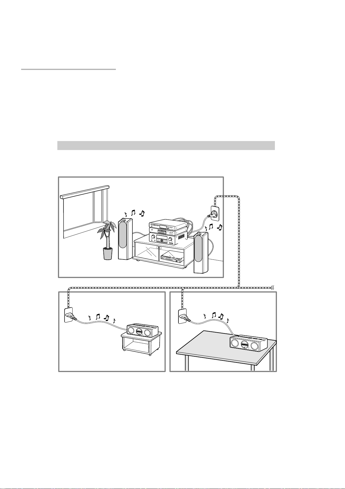
By simply plugging the power cables of the ZR6001 and ZC4001 into ordinary home electrical outlets, the ZR6001 sends
audio sources over your home electrical line for playback by the ZC4001.
PLC (POWER LINE COMMUNICATION)
The ZR6001* converts analog audio signals into noncompressed linear PCM digital signals, modulates them into high
frequency signals, and sends them over
power lines. The ZC4001 demodulates the sent signals and converts them back to analog signals.
* : If the condition of the power line degenerates because of the effects of noise from other devices or for other reasons,
the ZR6001 uses an audio format of different sampling rate and data bit length.
CONNECTIONS
CONNECTING FOR THE MULTI PLC LISTENING
Connect the AC power cable of the ZR6001 to a wall electrical outlet. Also connect the AC power cable of
the ZC4001 to a wall electrical outlet.
Up to four ZC4001 units may be connected to the same system at one time.
ROOM A
ZR6001
POW
ON
E
R
/S
TANDBY
PHO
N
ES
SU
R
ROUND
M
ODE
OPEN/
CL
OSE
PLAY
S
TOP
PAUSE
DVD
MEMORY
PREV.
VI
DEO
NEXT
MODE
BS
F/
DI
P
GI
TAL
TV
TUNING
FM/AM
1
Home power line
ROOM B ROOM C
ZC4001
ZC4001
6
Page 9
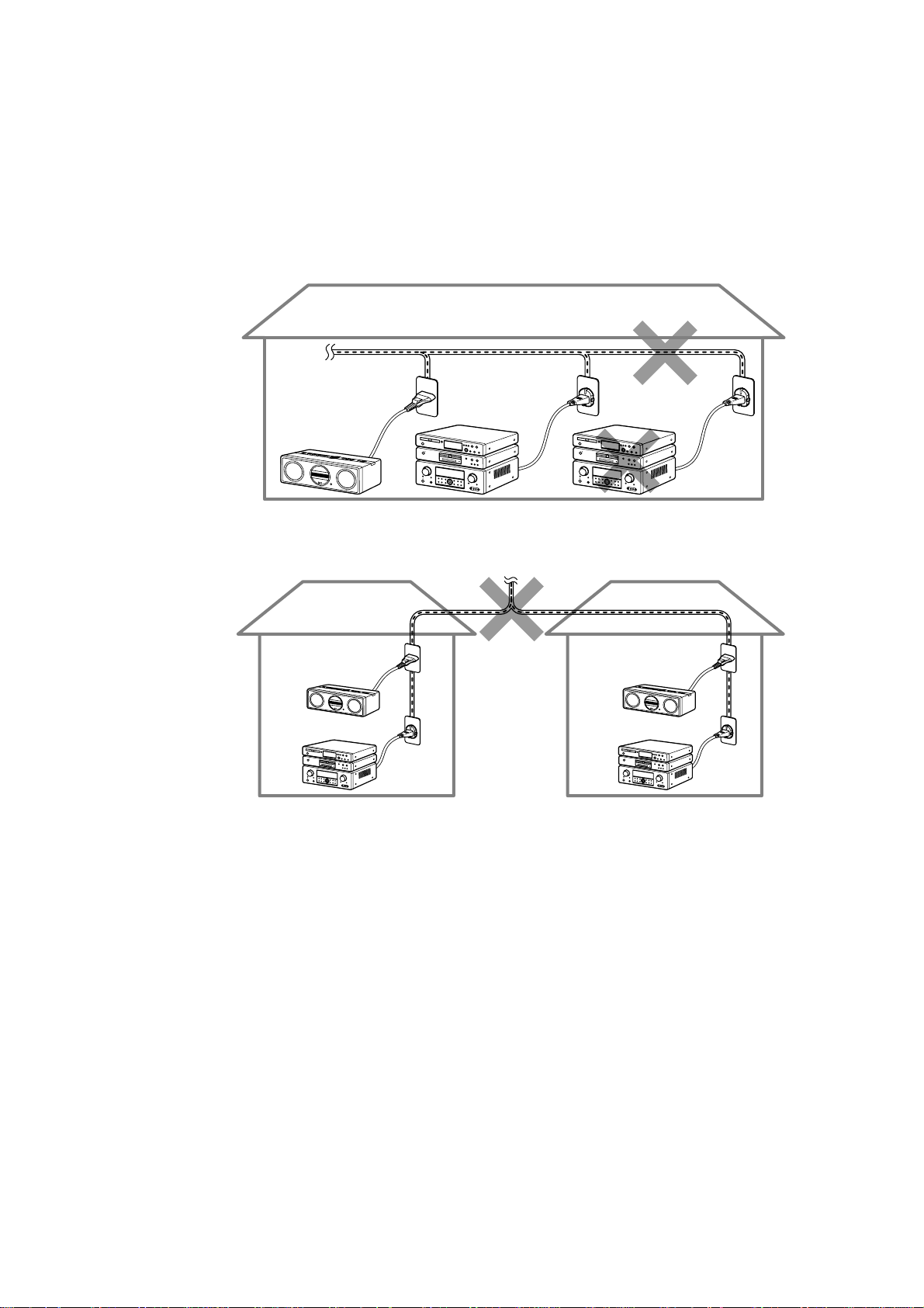
Notes:
• The ZR6001 sends audio data to the ZC4001 over power lines. Therefore, if the condition of the power line
degenerates seriously because of the effects of noise from other devices or for other reasons, audio data may
not be received or may skip.
• If the distance of the power line between the ZR6001 and ZC4001 is very long, audio data may not be received
or may skip.
• At the time of purchase, all ZC4001 and ZR6001 are set to the same Group ID. If used with this same Group
ID, you risk having your music listened into by others. Therefore, set the Group ID as explained herein.
• If the following trouble is experienced, block PLC signals from other sources using a commercially available
power filter, etc.
When a ZC4001 and ZR6001 are connected over PLC, another ZR6001 cannot be added to the same power
line and connected over PLC. In this case, PLC signals are not sent.
ZC4001
ZC4001
ZR6001
ZR6001
If a ZR6001 and ZC4001 are connected over PLC in a nearby apartment unit for example, and there is only
a short distance between your apartment and your neighbor’s, the PLC signals from your neighbor’s
apartment can travel over power lines to your place, mix with your system, and prevent audio output.
ZC4001
ZR6001
ZC4001
ZR6001
7
Page 10
POWER AMPLIFIER ADJUSTMENT
3.
Idling Current Alignment
1. Each of the measurement points are provided with the two test points. Set a digital Voltage meter to DC voltage
input, connect the meter to the test points at both contact points.
2. After the setup above, turn on the main switch.
3. Adjust variable resistors (VR41, VR42…VR71) according to the digital voltmeter readings. The target setting value is
the following table for each channel.
Settings: Master Volume — Minimum
Speaker out — No Load
Top lid — OPEN
Channel Alignment Point Measurement Point
Front L VR41 CN41
Center VR61 CN61
Front R VR51 CN51
Surround L VR42 CN42
Surround R VR52 CN52
Surround Back L VR62 CN62
Surround Back R VR71 CN71
Time Table of Idling Current Rise
Ambient temperature
After Turning ON
5 min. 1.2 mV ± 0.3 mV 2.0 mV ± 0.3 mV
10 min. 1.2 mV ± 0.3 mV 2.1 mV ± 0.3 mV
20 min. 1.4 mV ± 0.3 mV 2.5 mV ± 0.3 mV
30 min. 1.6 mV ± 0.3 mV 2.7 mV ± 0.3 mV
40 min. 1.7 mV ± 0.3 mV 2.9 mV ± 0.3 mV
50 min. 1.8 mV ± 0.3 mV 3.1 mV ± 0.3 mV
60 min. 1.9 mV ± 0.3 mV 3.2 mV ± 0.3 mV
10 to 19 degrees centigrade
Measurement Voltage Measurement Voltage
Ambient temperature
20 to 30 degrees centigrade
4. SERVICE MODE
Microprocessor (IC28), DSP(IC20 )Version and FLD Segment Check Mode.
1. While the power is on, MULTI, EXIT and 7.1CH INPUT buttons simultaneously more than 3 seconds.
The FL display shows "SERVICE MODE" for 2 seconds then shows the model name.
SERV I CE MODE
ZR6001
2. Press MULTI button, The software version of the MAIN microprocessor (IC28) is displayed in the format below.
V060306 IU
ear
Month
Date Dest.
(Dest. : Destination)
8
Page 11

Press MULTI button again, The software Type Number is displayed.
3.
SOFT TYPE XX
(XX is displayed in Hex)
4. Press MULTI button again, The Code Group Type Number is displayed.
CODE TYPEXXXX
(XXXX is displayed in Hex)
5. Press MULTI button again, The left half, right half and center of the label area in the FLD light on and off each other.
6. Press MULTI button again, The segments of the character area in the FLD flick in checker pattern.
7. Press MULTI button again, All the FL segments turns off.
8. Press MULTI button again. Every time MULTI button is pressed, DSP code is indicated in turn from NO.1 to NO.10.
CD01 02060105
SIGDev. TYP Ver.No.
No. : DISP CODE ID Dev. : Device ID SIG. : CODE SIG ID
TYP. : CODE TYPE ID Ver. : Version
9. Press MULTI button, The software version of the SUB microprocessor (IC19) is displayed in the format below.
SUB 060306.... 2
10. Press MULTI button, The Firmware version of the PLC Module is displayed in the format below.
P L C V 0. 4 0
11. Press MULTI button again to quit this mode.
Note: Step4, 5 is to check if CPU software is capable of DSP code. "Software Type No" is to show what "DSP Code
Group" CPU is capable of. And vice versa.
Step 8 is to manage the 16 codes for DSP.
• When the unit is once turned into Service Mode, the unit keeps this mode until the main power is turned off.
(Turning into stand-by mode does not make it quit from Service Mode.) When the unit quits from Service Mode,
Information in the memory is also cleared and the unit returns to the status when it is out from the factory.
Product Reset
To reset the back up memory of the unit into the default status, follow the procedure below.
1. Turn of the unit and press 7.1CH INPUT and MULTI button simultaneously more than 3 seconds or more.
2. After "DEFAULT" is displayed on FLD, power is turned off once and turned of again, EEPROM is cleared to the default
status, microprocessor is reset and the unit returns to the normal status. (Software Serial Number will not be cleared.)
Note: When the unit is shipped from the factory, the procedure above must be done to set the unit to initial status after the
tests.
9
Page 12

SYSTEM ERROR
5.
When the microcomputer detects a trouble, the following information is displayed on the FLD.
• After the error contents indication, Surround Mode is
initialized and returned Factory mode.
• The contents of the ERROR indication are the followings.
1. Trouble in DSP
If communication with DSP is troubled more than 2 seconds.
CHECK DSP
2. Trouble in DSP Code
The trouble of DSP Code was found.
CHECK DSP ROM
3. Trouble in ADC
When ADC input was chosen and CAL signal continued High about 2 seconds after the ADC Calibration start.
CHECK ADC
4. Trouble in EEP-ROM
If data from EEPROM does not match.
CHECK E2P
5. Trouble in EEP-ROM IF
If communication with EEPROM is troubled more than 2 seconds.
CHECK E2P I F
6. Trouble in RS-232C
If communication of Panja with RS232C is troubled more than 2 seconds.
CHECK 232C
7. Trouble in 5V Supply
If 5V supply to DATA DIR is troubled.
CHECK POW5
8. Trouble in Protection
CPU turns off the speaker output.
PROTECT
10
Page 13
6. UPDATE FIRMWARE
[A] SOFTWARE (fdtv30300.exe) DOWNLOAD AND INSTALL PROCEDURE
DOWNLOADS OF THE SOFTWARE (Flash Development Toolkit: the rest is FDT)
Download the software for update of the SUB CPU.
Launch the browser. Type http://www.renesas.com/ into an address. And press Enter.
NOTE : This site is managed by RENESAS. The following explanation may differ from the actual composition.
When different, please proceed along with the site composition of RENESAS. When FDT cannot be found, please
search "Flash Development Toolkit", or type http://download.renesas.com/eng/mpumcu/index.html into an address.
Click the SUPPORT on the site of RENESAS(GLOBAL SITE).
Click the SUPPORT on the site of Renesas.
11
Page 14
k the Software download for tools on Support.
Clic
12
Page 15
k the Agree on AGREEMENT. And click Submit.
Chec
13
Page 16
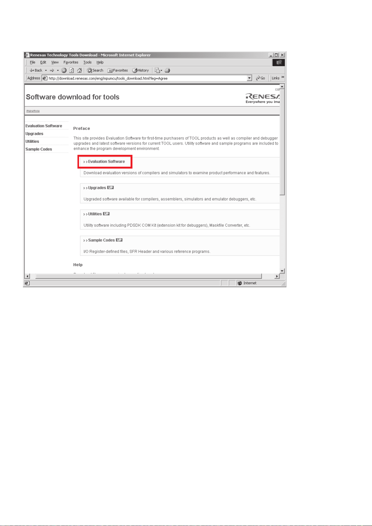
k Evaluation Software.
Clic
14
Page 17

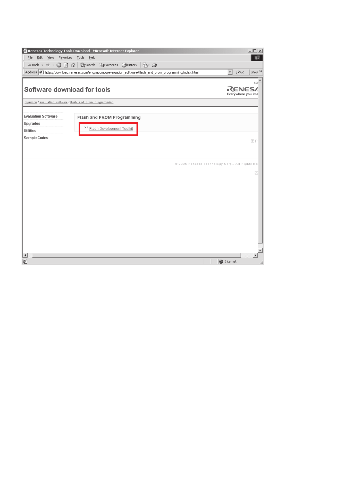
k Flash and PROM Programming.
Clic
15
Page 18
k Flash Development Toolkit.
Clic
16
Page 19
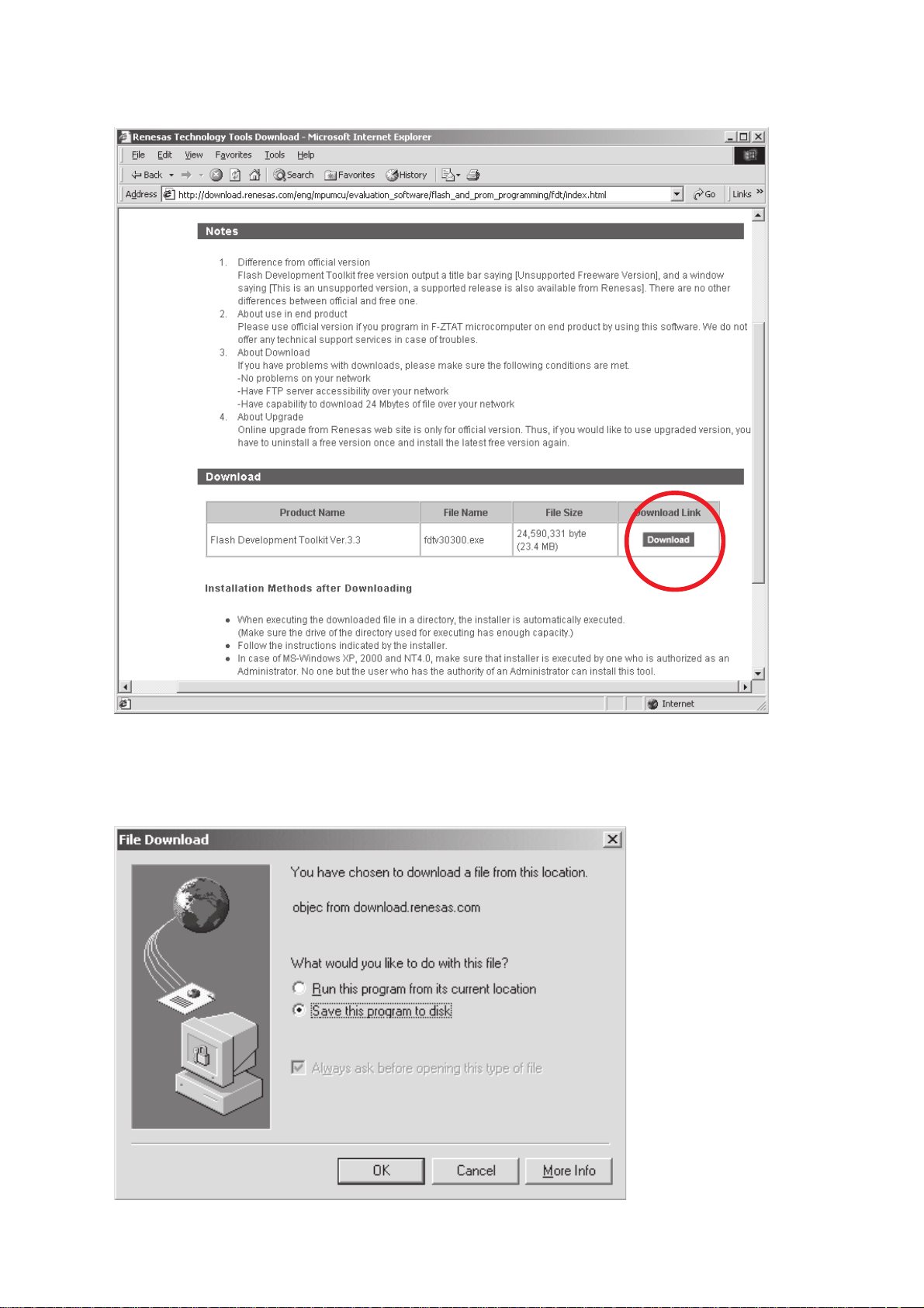
k Download.
Clic
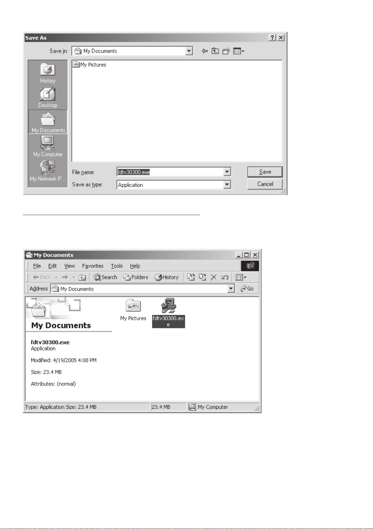
Save the fdtv30300.exe on your PC’s hard disc.
NOTE : A file name is changed by improvement.
17
Page 20
INSTALLS OF THE SOFTWARE (Flash Development Toolkit Ver.3.3)
Open the folder with the downloaded file.
And double click the fdtv30300.exe.
18
Page 21
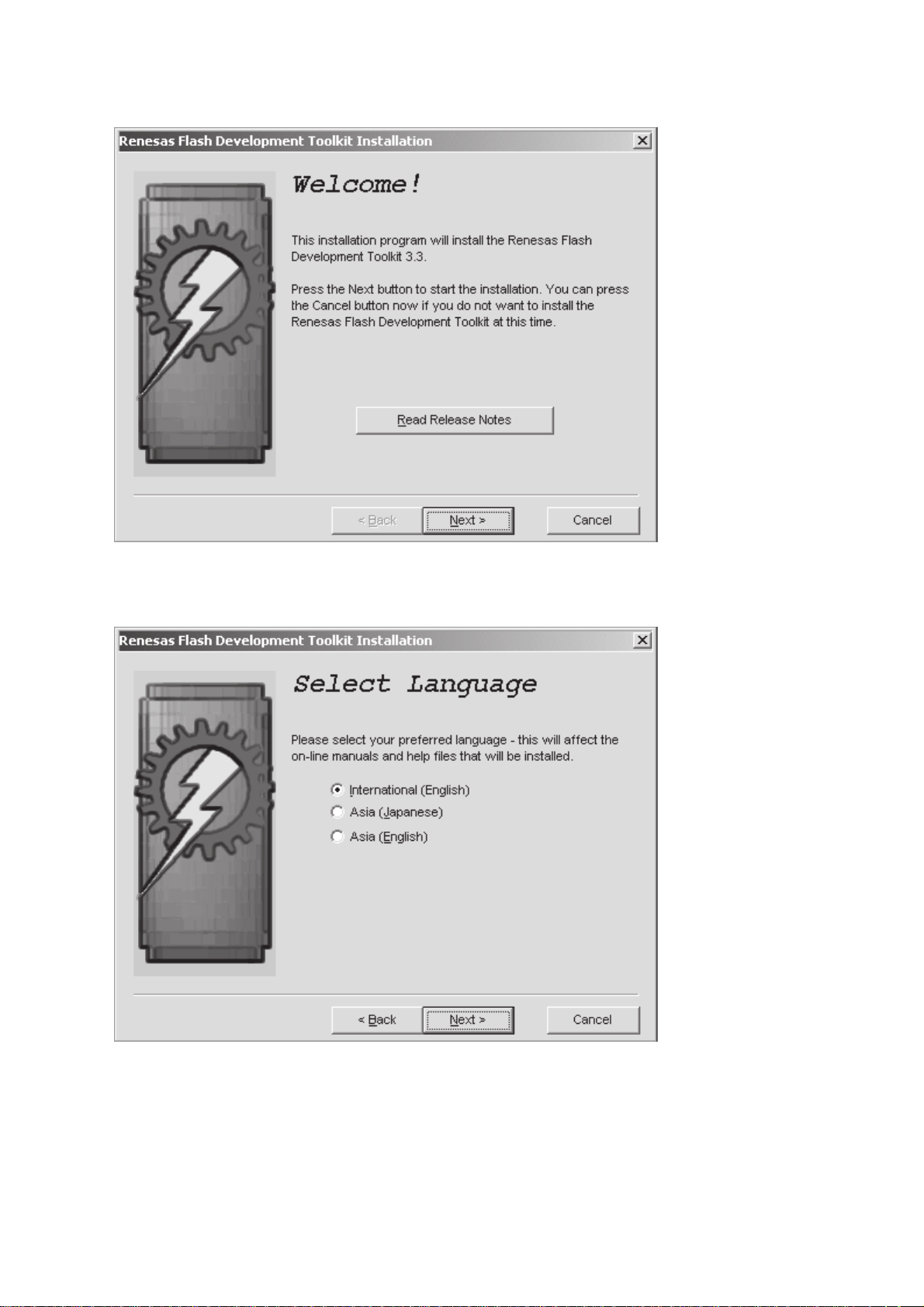
Clic
k Next >.
Choose the language. And click Next >.
19
Page 22
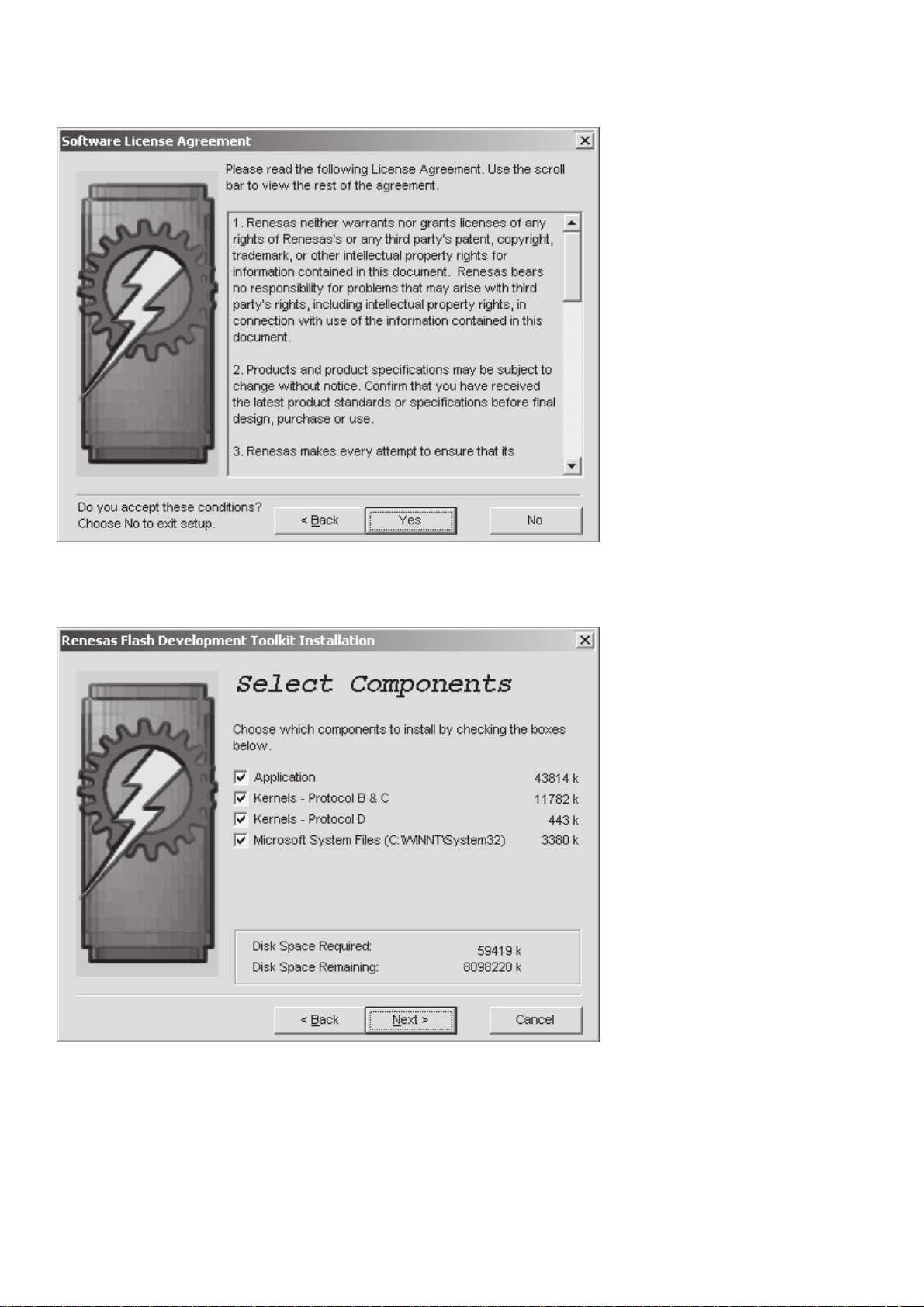
Clic
k Yes.
Click Next >.
20
Page 23
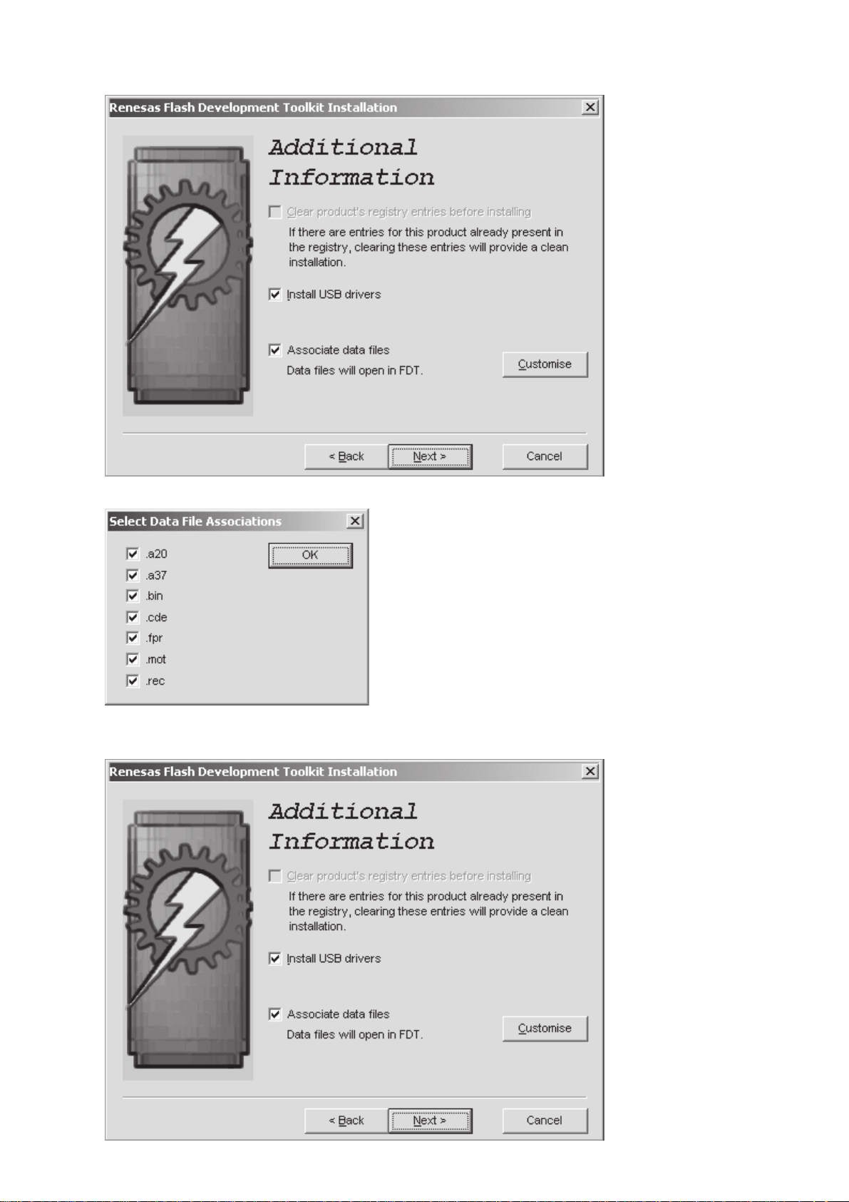
k Customise.
Clic
Check to the all check box. And click OK.
Click Next >.
21
Page 24
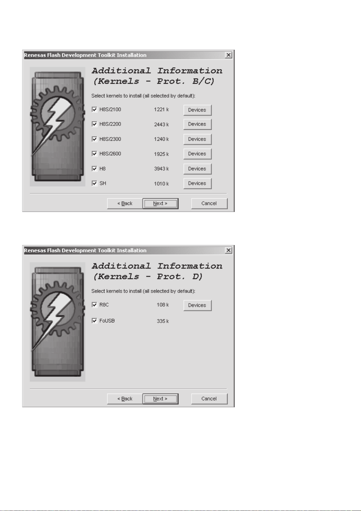
k to the all check box. And click Next >.
Chec
Click Next >.
22
Page 25
Clic
k Next >.
Click Next >.
23
Page 26
Clic
k Next >.
Click Install.
24
Page 27
The status bar appears
Click Finish.
.
25
Page 28

B] WRITING AND UPDATE SOFTWARE
[
Software for MAIN CPU, SUB CPU, DSP and PLC firmware can be updated.
Have update application software. ("H8Download.exe", "fdtv30300.exe (FDT3.3) or latest version", "PlcFirmUpdate.exe"
and "UpgradeDSP.exe")
There are four mode of download, regarding to the target of software as bellow.
• Mode 1: Update DSP's software to 4M Flash-ROM.
This mode is to update the software for DSP.
The target devise is 4M Flash-ROM (IC20) on CUP11859Z (DSP PWB).
The unit needs to be set update condition, by three front keys.
The updating of software takes about 2 minutes.
• Mode 2: Update MAIN CPU's software to internal Flash-ROM.
This mode is to update the software for MAIN CPU.
The target devise is internal flash ROM of CPU (IC28) on CUP11859Z (DSP PWB).
The unit needs to be set to writing condition, by pushing internal switch from rear panel.
The updating of software takes about 2 minutes and 30 seconds.
• Mode 3: Update SUB CPU's software to internal Flash-ROM.
This mode is to update the software for SUB CPU.
The target devise is internal flash ROM of CPU (IC19) on CUP11861Z (PLC PWB).
The unit needs connection to download JIG.
The unit needs to be set update condition, by three front keys.
The updating of software takes about 15 seconds.
• Mode 4: Update PLC’s firmware to PLC MODULE.
This mode is to update the firmware for PLC.
The target devise is PLC MODULE (MLD011TM-C2 00MZK11CW0010).
The unit needs connection to download JIG.
The unit needs to be set update condition, by three front keys.
The updating of software takes about 1 minute.
NECESSARY EQUIPMENT
The following items are required for updating.
Windows PC (OS: Windows2000 or WindowsXP) with Serial port.
RS-232C Dsub-9 pin cable (female to female/straight type)
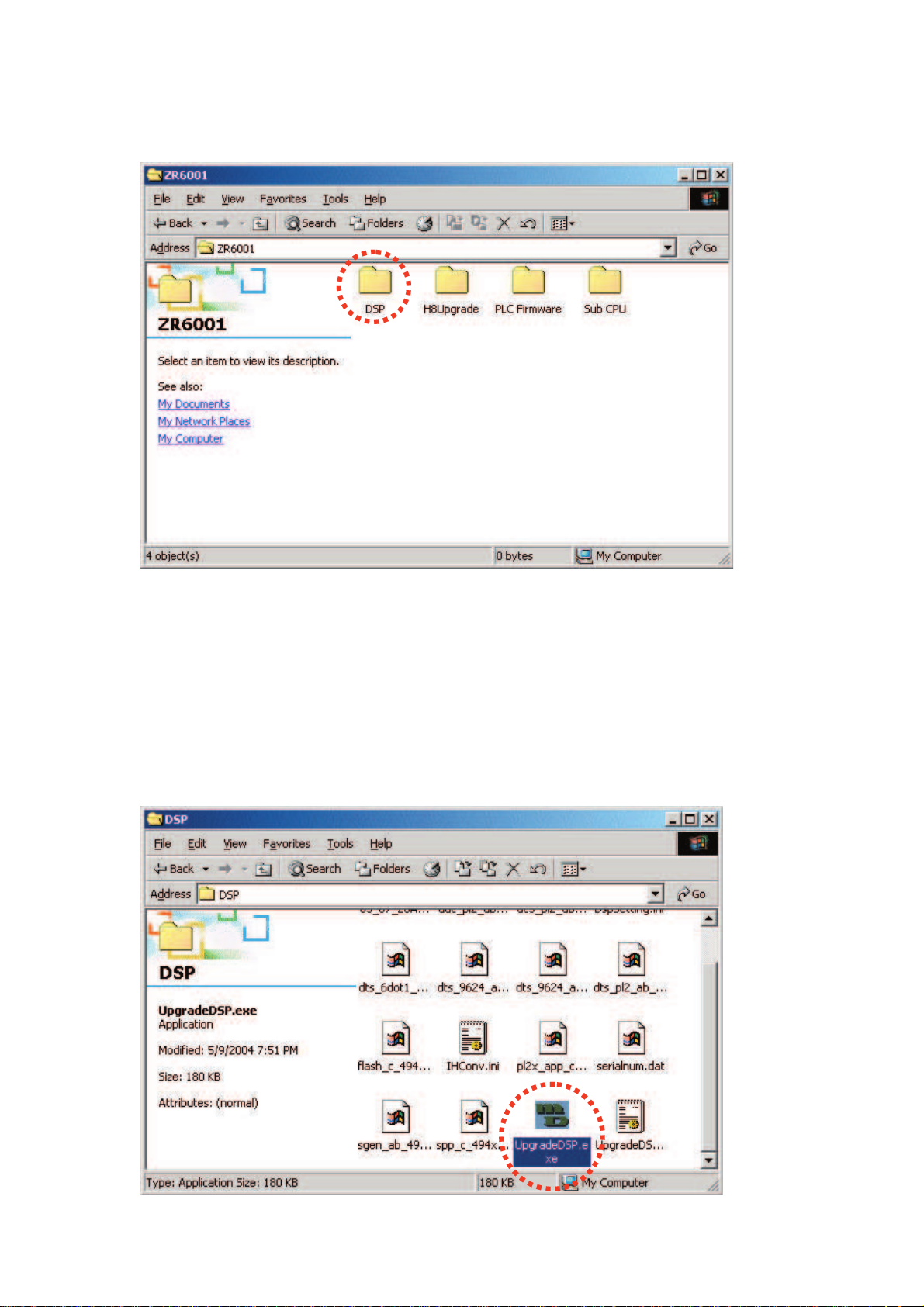
Update software to MAIN CPU. (H8Download.exe, etc... in H8Upgrade folder)
Update software to SUB CPU. (update data in SUB CPU folder)
Update software to DSP. (UpgradeDSP.exe, etc... in DSP folder)
Update firmware to PLC. (PlcFirmUpdate.exe, etc... in PLC firmware folder)
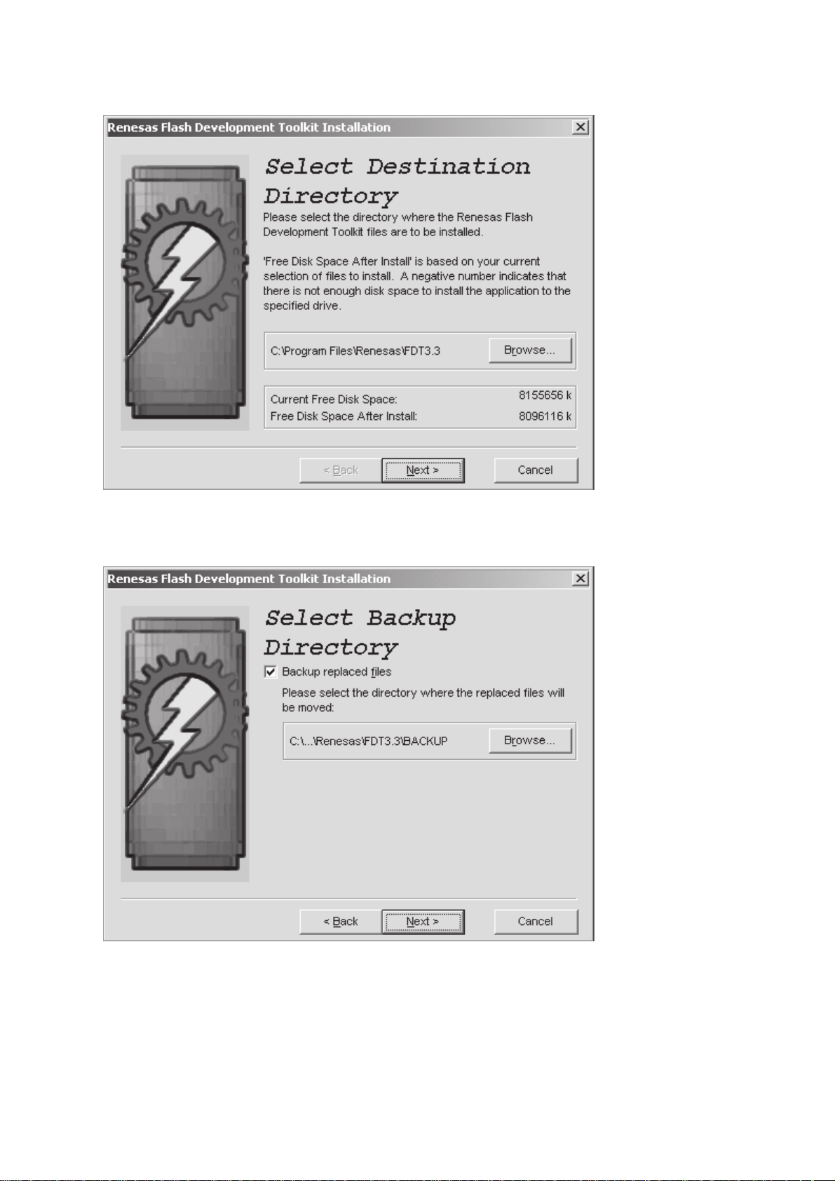
Flash Development Toolkit 3.3 or latest version (fdtv30300.exe or latest version)
PLC download JIG (90M-ZR6001JIG)
Use RS232C Dsub-9 pin cable (female to female/straight type) to connect PC and the RS-232C port in rear panel of the
unit, when updating MAIN CPU and DSP.
Use RS232C Dsub-9 pin cable (female to female/straight type) to connect PC and the download JIG, when updating SUB
CPU and PLC firmware.
Serial port on PC needs to be set by dialog box for each program. Serial port can be set from COM1 to COM5.
26
Page 29
ode 1: Update DSP’s software to 4M Flash-ROM
M
Download Firmware for DSP (Mode 1)
1. Put the "DSP" folder into anywhere on your PC's hard disc.
2. Connect RS-232C on the rear panel of the unit and Serial Port of windows PC with RS-232C cable.
3. Turn on the unit, and wait for about 10 seconds.
4. Press ENTER, MUTE and T-MODE buttons simultaneously more than 5 seconds to turn the unit into Loading Mode.
5. "LOADING MODE" is shown on FLD.
6. Double click the UpgradeDSP.exe. And Launch the marantz UpgradeDSP.
27
Page 30

Cl i c k Port setting.
7.
8. Choose the COM Port No.
9. Choose 38400 in the Baud rate.
28
Page 31

0. Click Start communication.
1
11. If the connection is made successfully, a dialog box saying "Success to connect" appears and "CONNECTED" is
displayed on FLD.
Click OK.
12. Click Send the DSP codes.
29
Page 32

3. Progress status of updating will be shown on PC and LOADING is displayed on FLD.
1
14. If updating is completed successfully, "COMPLETED" is displayed on FLD. And a dialog box saying "Finished the DSP
code transmitting" appears.
Click OK and then Application is closed automatically.
15. Turn off the unit. And disconnect mains cord from the unit.
30
Page 33

ode 2: Update MAIN CPU’s software to internal Flash-ROM
M
Download software for MAIN CPU (Mode 2)
1. Put the "H8Upgrade" folder into anywhere on your PC's hard disc.
2. Connect RS-232C on the rear panel of the unit and Serial Port of windows PC with RS-232C cable.
3. Insert a thin rot to the hole and push the switch (SW10) inside to turn on the switch.
Hole of rear panel
4. Turn on the unit.
Note : When the unit is into boot mode, stand-by LED is not lights up.
31
Page 34

Double click the H8Download.exe. And launch the marantz firmware upgrade program.
5.
7. C l i ck Set ports.
8. Choose the COM Port No.
32
Page 35

Click other files... from Firmware program file.
9.
10. Choose Zr6001Main_yymmdd.mot. And click Open.
REMARK : yy is two digits of year. mm is month. dd is date.
11. Click Connect.
33
Page 36

2. If the connection with the H8 µ-P is successfully made, a dialogue box saying "Success to the H8 micro processor
1
connection" appears. If the connection fails, error message will appear.
Click OK.
13. Click Send to start update.
14. If the firmware is updated successfully, a dialog box saying "Finished the firmware program sending" appears.
Click OK.
34
Page 37

5. Click Close to close the application.
1
16. Turn off the unit. And disconnect FPC of the connection JIG from the unit.
17. Insert a thin rot to the hole and push the switch (SW10) inside to turn off the switch.
Firmware Version Check
To check the versions of the firmware, see "Microprocessor (CPU), DSP Version and FLD Segment Check Mode" in "4.
SERVICE MODE" section.
35
Page 38

ode 3: Update SUB CPU’s software to internal Flash-ROM.
M
Download software for SUB CPU (Mode 3)
The writing software setup procedure
1. Launch the Flash Development Toolkit (FDT).
Note : Please refer to "[A] SOFTWARE (fdtv30300.exe) DOWNLOAD AND INSTALL PROCEDURE", when you do
not have FDT.
2. Click Start, Programs, Renesas, Flash Development Toolkit 3.3 and Flash Development Toolkit 3.3.
3. Check Create a new project workspace, and click OK.
Note : It is needs setup for ZR6001. When you have already setup, please move on to "Writing Procedure for SUB
CPU".
36
Page 39

4. ZR6
001_SUB_CPU is inputted into the Workspace Name.
(It is simultaneously inputted into Project Name.)
Click OK.
5. Choose the H8 /36049F in Select Device.
Click Next.
37
Page 40

. Choose the Serial port No. in the Select Port.
6
Click Next.
7. 20.0000 is inputted into the Enter the CPU crystal frequency for the selected device.
Click Next.
38
Page 41

Check The BOOT Mode in Select Connection.
8.
Check Recommended Speeds and Use Default, and click Next.
9. Check the Automatic in Protection.
Check the Advanced in Messaging.
Click Finish.
39
Page 42

riting Procedure for SUB CPU
W
1. Disconnect the mains cord from the unit.
2. Connect RS-232C on the download jig and Serial Port of windows PC with RS-232C cable.
3. Connect FPC from download jig to update connector in rear panel of the unit.
Update connector for
SUB CPU and PLC
FPC of download jig
Download jig
RS-232C cable
4. Connect the mains cord into the unit.
5. Launch the Flash Development Toolkit (FDT). (When FDT is not launch.)
Note : When FDT is already launch, please move to No.18.
40
Page 43

Click Start, Programs, Renesas, Flash Development Toolkit 3.3 and Flash Development Toolkit 3.3.
6.
7. C h e ck Browse to another project workspace, and click OK .
8. Choose ZR6001_SUB_CPU.AWS in ZR6001_SUB_CPU folder under workspace folder.
And click Open.
41
Page 44

. Right button of mouse click on the ZR6001_SUB_CPU, and select the Add Files... in a menu.
9
10. Choose the Zr6001Sub_yymmdd.mot, and click Add.
11. Turn on the unit, and wait for about 10 seconds.
12. Press ENTER, (Right arrow) and MUTE button simultaneously more than 5 seconds, and turn on update mode.
13. "SUB SYS LOAD" is shown on FLD.
42
Page 45

4. Click Device in the menu bar and select Connect to Device.
1
15. Press right button of mouse on the Zr6001Sub_yymmdd.mot, and select the Download File in a menu.
43
Page 46

6. Software is written into the SUB CPU.
1
17. The writing of software takes about 15 seconds.
44
Page 47

8. Click Device in the menu bar and select Disconnect.
1
19. Click File and select Exit in menu, when ending writing software.
20. Disconnect the mains cord from the unit. And disconnect the FPC of download jig.
45
Page 48

ode 4: Update PLC’s firmware to PLC MODULE
M
Download firmware for PLC (Mode 4)
1. Disconnect the mains cord from the unit.
2. Connect RS-232C on the download jig and Serial Port of windows PC with RS-232C cable.
3. Connect FPC from download jig to update connector in rear panel of the unit.
Update connector for
SUB CPU and PLC
FPC of download jig
Download jig
4. Connect the mains cord into the unit.
5. Turn on the unit, and wait for about 10 seconds.
6. Press ENTER,
7. "PLC FW LOAD" is shown on FLD.
(Left arrow) and MUTE button simultaneously more than 5 seconds. And turn on update mode.
RS-232C cable
46
Page 49

. Put the "PCL Firmware" folder into anywhere on your PC's hard disc.
8
9. Double click TxPlcUpdate folder.
47
Page 50

0. Double click the PlcFirmUpdate.exe. And Launch the PLC Firmware Update.
1
11. Click Connect.
48
Page 51

2. When "CONNECTED" appear in STATUS, connection is success.
1
Click UPDATE.
13. Firmware is written into the PLC MODULE.
The writing of firmware takes about 1 minute.
14. Click OK.
49
Page 52

5. Click QUIT.
1
16. Disconnect the mains cord from the unit. And disconnect the FPC of download jig.
50
Page 53

7. WIRING DIAGRAM
51 52
Page 54

8. BLOCK DIAGRAM
5453
Page 55

9. SCHEMATIC DIAGRAM
INPUT PWB
55 56
Page 56

DSP PWB (1/2)
5857
Page 57

DSP PWB (2/2)
59 60
Page 58

PLC IR-RX PWB
ENCORDER PWB
TACT
PWB
FRONT PWB
ST-BY PWB
H / P PWB
7.1-CH PREOUT PWB
PUSH SW PWB
6261
Page 59

VIDEO PWB
63 64
Page 60

COMPONENT PWB
6665
Page 61

VIDEO CONVERTER PWB
67 68
Page 62

AMP PWB
7069
Page 63

POWER PWB
71 72
Page 64

PLC PWB
7473
Page 65

10. PARTS LOCATION
75 76
Lead-free Solder
When solder
ing, use the Lead-free Solder (Sn-Ag-Cu).
Page 66

Lead-free Solder
When solder
ing, use the Lead-free Solder (Sn-Ag-Cu).
7877
Page 67

79 80
Lead-free Solder
When solder
ing, use the Lead-free Solder (Sn-Ag-Cu).
Page 68

IC14
Q100
Q110Q106
Q108Q104
IC16
Q101
VIDEO CONVERTER PWB A
IC13
IC11
IC12
Lead-free Solder
When solder
ing, use the Lead-free Solder (Sn-Ag-Cu).
Q111
Q102
Q107
Q105Q109
Q103
VIDEO CONVERTER PWB B
8281
Page 69

Q723
Q707 Q709 Q717
AMP PWB
Q721 Q620 Q622
Q624 Q623 Q524 Q523 Q424 Q423
Q616Q715 Q713 Q711
Q614 Q612 Q607 Q609 Q617
Q608
Q610 Q618 Q615 Q613 Q611
Q619 Q621 Q520 Q522 Q519 Q521 Q420 Q422 Q419 Q421Q719
Q508 Q510 Q518
Q516 Q514 Q512
IC61 IC51 IC41
Q603 Q605 Q504 Q503 Q505 Q404 Q406 Q403 Q405 Q801
Q506Q604Q606Q703Q705 IC71
Q507 Q509 Q517
Q515 Q513 Q511
Q408 Q410 Q418
Q416 Q414 Q412
Q407 Q409 Q417 Q805 Q806
Q415 Q413 Q411
Q807
Q802Q803Q804
83 84
Lead-free Solder
When soldering, use the Lead-free Solder (Sn-Ag-Cu).
Page 70

Lead-free Solder
When solder
ing, use the Lead-free Solder (Sn-Ag-Cu).
8685
Page 71

87 88
Page 72

About this PWB (MODULE) repair:
There are no component parts for repair.
Please replace this PWB ASSY (PLC MODULE) with the new
one.
PLC MODULE A
PLC MODULE B
Lead-free Solder
When soldering, use the Lead-free Solder (Sn-Ag-Cu).
9089
Page 73

IC DATA
11.
IC21 : TC9162,3,4
91
Page 74

IC21 :
TC9162,3,4
92
Page 75

IC22 :
TC9273
IC24 : TC9499
93
Page 76

IC12 :
TC90A49F
94
Page 77

IC13 : MM1511
IC14 :
TA1270BF
95
Page 78

IC35 :
CS5361
SCLK
VCOM LRCK
REFGND
V
L
SDOUT MCLK
RST
M/
LRCK
SCLK
MCLK
VD
GND
VL
SDOUT
DIV
HPF
DIF
Pin Name
RST
M/S
LRCK
SCLK
MCLK
VD
GND
VL
SDOUT
DIV
124
223
S
322
421
520
619
718
817
916
10 15
11 14
12 13
I/O
I
I
I
I
I
I
I
I
O
I
Pin Description
#
Reset
1
Master/Slave Mode
2
Left Right Clock
3
serial audio data line. The frequency of the left/right clock must be at the audio sample rate, Fs.
Serial Clock
4
Master Clock
5
several standard audio sample rates and the required master clock frequency.
Digital Power
6
ing Conditions for appropriate voltages.
Ground
7,18
Logic Power
8
ommended Operating Conditions for appropriate voltages.
Serial Audio Data Output
9
MCLK Divider
10
FILT+
REFGND
FILT+
Voltage Reference
VCOM
+
AINR
AINR
VA
GND
-
AINL-
AINL+
S/H
+
LP Filter
-
AINLAINL+
TST
M1
AINR-
AINR+
S/H
+
-
M0
(
) - The device enters a low power mode when low.
Input
-In Slave mode, LRCK and SCLK become input. (FIXED LOW)
(Input)
(
) - Determines which channel, Left or Right, is currently active on the
Input
(
) - Serial clock for the serial audio interface.
Input
(
) - Clock source for the delta-sigma modulator and digital filters. Table 1 illustrates
Input
(
)-Positive power supply for the digital section. Refer to the Recommended Operat-
Input
(
) - Ground reference. Must be connected to analog ground.
Input
(
)- Determines the required signal level for the digital input/output. Refer to the Rec-
Input
) - (FIXED LOW)
(Input
(
) - Output for two’s complement serial audio data.
Output
DAC
DAC
Se rial O utput Inte rfac e
Q
QLP Filter
Digital
Decimation
Filter
Digital
Decimation
Filter
High
Pass
Filter
High
Pass
Filter
RST
DIF
M/S
HPF
DIV
MODE0
MODE1
HPF
DIF
M0
M1
TST
AINL+
AINL-
VA
AINR+
AINR-
VCOM
REF_GND
FILT+
I
I
I
I
I
I
I
I
I
I
O
I
O
High Pass Filter Enable
11
the indeterminate DC offsets introduced by the analog buffer stage and the analog modulator. The firstorder high pass filter response characteristics are detailed in the Digital Filter specifications table. The filter response scales linearly with sample rate.
Digital Interface Format
12
and serial data is defined by the Digital Interface Format selection. Refer to Figures 8 and 9.
Mode Selection
13,
14
(FIXED LOW)
Test Pin
15
Differential Left Channel Analog Input
16,
modulators via the AINL+/- pins. The full scale differential analog input level is specified in the Analog
17
Characteristics Specification table.
Analog Power
19
ating Conditions for appropriate voltages.
Differential Right Channel An alog In put
20,
modulators via the AINR+/- pins. The full scale differential analog input level is specified in the Analog
21
Characteristics Specification table.
Common Mode Voltage
22
the common mode voltage of the CS5361. VCOM is not buffered and the maximum current is 10 uA.
Reference Ground
23
to analog ground.
Positive Voltage Reference
24
Requires the capacitive decoupling to GND as shown in the Typical Connection Diagram.
(Input)
(
) -(FIXED LOW)
Input
-
This pin needs to be connected to GND.
(
)-Positive power supply for the analog section. Refer to the Recommended Oper-
Input
(
Input
) -
(Input
(
(Output)
) - Ground reference for the internal sampling circuits and must be connected
The device includes a high pass filter after the decimator to remove
) - The required relationship between the Left/Right clock, serial clock
Input
) - Signals are presented differentially to the delta-sigma
(
Input
(
) -Signals are presented differentially to the delta-sigma
Input
-
Nominally 2.5 volts; can be used to bias the analog input circuitry to
Output
-
)
Positive reference voltage for the internal sampling circuits.
(
96
Page 79

IC16 :
CS4382
97
Page 80

IC16 :
CS4382
98
Page 81

IC19 :
CS49403
Compressed
Audio
Interface
Digital
Audio
Interface
DSP AB
PLL Clock
Manager
Frame
Shifter
Input
Buffer
RAM
Programmable
Multistandard
Audio Decoder
Parallel or Serial
Host Interface
Shared Memory
SAI 0
SAI 1
SAI 3
SAI 2
DSP C
32-Bit DSP
DSP
RAM
Debug Port
Serial
Audio
Interface
DSP
ROM
Interface
Internal Bus
External Memory
Interface
Digital
DAO 0
Audio
DAO 1
GPIO and I/O
Controller
Parallel or Serial
Host Interface
Pin
I/O Function Description
No.
1 I/O UHS0, GPIO18 Mode Select Bit 0, General Purpose I/O
2 I/O UHS1, GPIO19 Mode Select Bit 1, General Purpose I/O
3 INTREQ Control Port Interrupt Request
4 I FA1, FSCDIN Host Address Bit One or SPI Serial Control Data Input
5 I/O GPIO20 General Purpose I/O
6 I FA0, FSCCLK Host Parallel Address Bit Zero or Serial Control Port Clock
7 I/O FHS2,
FSCDIO,
FSCDOUT
8 I/O GPIO21 General Purpose I/O
9 FDAT7 DSP AB Bidirectional Data Bus
10 VDD6 2.5V Supply Voltage
11 VSS6 2.5V Ground
12 FHS0, FWR,
FDS
13 O FHS1, FRD,
FR/W
14 FDAT6 DSP AB Bidirectional Data Bus
15 I FCS Host Parallel Chip Select, Host Serial SPI Chip Select
16 O FINTREQ Control Port Interrupt Request
17 FDBCK Reserved
18 FDAT5 DSP AB Bidirectional Data Bus
19 FDAT4 DSP AB Bidirectional Data Bus
20 VDD7 2.5V Supply Voltage
21 VSS7 2.5V Ground
22 FDAT3 DSP AB Bidirectional Data Bus
23 FDBDA Reserved
24 FDAT2 DSP AB Bidirectional Data Bus
25 DBDA Debug Data
26 DBCK Debug Clock
27 FDAT1 DSP AB Bidirectional Data Bus
28 TEST Reser ved
29 FDAT0 DSP AB Bidirectional Data Bus
30 I/O NV_WE,
GPIO16
31 I/O NV_OE,
GPIO15
32 I/O NV_CS,
GPIO14
33 SD_WE SDRAM Write Enable
34 SD_DATA0,
EXTD0
35 SD_DATA1,
EXTD1
36 SD_DATA2,
EXTD2
37 SD_DATA3,
EXTD3
38 SD_DATA4,
EXTD4
39 SD_DQM0 SDRAM Data Mask 2
40 SD_DATA5,
EXTD5
41 VSSSD4 3.3V SDRAM/SRAM/EPROM Interface Ground
42 VDDSD4 3.3V SDRAM/SRAM/EPROM Interface Supply
43 SD_DATA6,
EXTD6
44 SD_DATA7,
EXTD7
45 SD_DQM1 SDRAM Data Mask 1
46 SD_DATA15,
EXTA18
47 SD_DATA14,
EXTA17
48 NC5 No Connect
49 SD_DATA13,
EXTA16
50 VSSSD3 3.3V SDRAM/SRAM/EPROM Interface Ground
51 VDDSD3 3.3V SDRAM/SRAM/EPROM Interface Supply
52 SD_DATA12,
EXTA15
Mode Select Bit 2 or Serial Control Port Data Input and
Output, Parallel Port Type Select
Mode Select Bit 0 or Host Write Strobe or Host Data Strobe
Mode Select Bit 1 or Host Parallel Output Enable or Host
Parallel R/W
SRAM Write Enable, General Purpose I/O
SRAM Output Enable, General Purpose I/O
SRAM Chip Select, General Purpose I/O
SDRAM Data Bus, SRAM External Data Bus
SDRAM Data Bus, SRAM External Data Bus
SDRAM Data Bus, SRAM External Data Bus
SDRAM Data Bus, SRAM External Data Bus
SDRAM Data Bus, SRAM External Data Bus
SDRAM Data Bus, SRAM External Data Bus
SDRAM Data Bus, SRAM External Data Bus
SDRAM Data Bus, SRAM External Data Bus
SDRAM Data Bus, SRAM External Address Bus
SDRAM Data Bus, SRAM External Address Bus
SDRAM Data Bus, SRAM External Address Bus
SDRAM Data Bus, SRAM External Address Bus
53 SD_DATA11,
EXTA14
54 SD_DATA10,
EXTA13
55 SD_DATA9,
EXTA12
56 SD_DATA8,
EXTA11
57 VSSSD2 3.3V SDRAM/SRAM/EPROM Interface Ground
58 VDDSD2 3.3V SDRAM/SRAM/EPROM Interface Supply
59 O SD_CLK_OUT SDRAM Clock Output
60 SD_ADDR9,
EXTA9
61 I SD_CLK_IN SDRAM Re-timing Clock Input
62 SD_ADDR8,
EXTA8
63 SD_ADDR7,
EXTA7
64 SD_CLK_EN SDRAM Clock Enable
65 SD_ADDR6,
EXTA6
66 SD_ADDR5,
EXTA5
67 SD_ADDR4,
EXTA4
68 SD_CS SDRAM Chip Select
69 VSSSD1 3.3V SDRAM/SRAM/EPROM Interface Ground
70 VDDSD1 3.3V SDRAM/SRAM/EPROM Interface Supply
71 SD_BA,
EXTA19
72 SD_ADDR10,
EXTA10
73 SD_ADDR0,
EXTA0
74 SD_ADDR1,
EXTA1
75 SD_ADDR2,
EXTA2
76 SD_ADDR3,
EXTA3
77 SD_RAS SDRAM Row Address Strobe
78 SD_CAS SDRAM Column Address Strobe
79 I/O SDATAN3,
GPIO27
80 I/O SDATAN2,
GPIO26
81 I/O SDATAN1,
GPIO25
82 I/O SDATAN0,
GPIO24
83 NC4 No Connect
84 NC3 No Connect
85 I/O LRCLKN,
GPIO23
86 I/O SCLKN,
GPIO22
87 O LRCLK1 Audio Output Sample Rate Clock
88 NC2 No Connect
89 NC1 No Connect
90 VDD1 2.5V Supply Voltage
91 VSS1 2.5V Ground
92 I/O AUDATA7,
XMT958B,
GPIO31
93 I/O AUDATA6,
GPIO30
94 I/O AUDATA5,
GPIO29
95 I/O HDATA7,
GPIO7
96 I/O HDATA6,
GPIO6
97 I/O HDATA5,
GPIO5
98 O SCLK1 Audio Output Bit Clock
SDRAM Data Bus, SRAM External Address Bus
SDRAM Data Bus, SRAM External Address Bus
SDRAM Data Bus, SRAM External Address Bus
SDRAM Data Bus, SRAM External Address Bus
SDRAM Address Bus, SRAM External Address Bus
SDRAM Address Bus, SRAM External Address Bus
SDRAM Address Bus, SRAM External Address Bus
SDRAM Address Bus, SRAM External Address Bus
SDRAM Address Bus, SRAM External Address Bus
SDRAM Address Bus, SRAM External Address Bus
SDRAM Bank Address Select, SRAM External Address Bus
SDRAM Address Bus, SRAM External Address Bus
SDRAM Address Bus, SRAM External Address Bus
SDRAM Address Bus, SRAM External Address Bus
SDRAM Address Bus, SRAM External Address Bus
SDRAM Address Bus, SRAM External Address Bus
PCM Audio Input Data, General Purpose I/O
PCM Audio Input Data, General Purpose I/O
PCM Audio Input Data, General Purpose I/O
PCM Audio Input Data, General Purpose I/O
PCM Audio Input Sample Rate Clock, General Purpose I/O
PCM Audio Input Bit Clock, General Purpose I/O
Digital Audio Output 7, S/PDIF Transmitter, General Purpose
I/O
Digital Audio Output 6, General Purpose I/O
Digital Audio Output 5, General Purpose I/O
DSP C Bidirectional Data Bus, General Purpose I/O
DSP C Bidirectional Data Bus, General Purpose I/O
DSP C Bidirectional Data Bus, General Purpose I/O
99
Page 82

CS49403
IC19 :
99 MCLK Audio Master Clock
100 VDD2 2.5V Supply Voltage
101 VSS2 2.5V Ground
102 I/O AUDATA4,
GPIO28
103 I/O HDATA4,
GPIO4
104 O SCLK0 Audio Output Bit Clock
105 I/O HDATA3,
GPIO3
106 O AUDATA3,
XMT958A
107 O AUDATA2 Digital Audio Output 2
108 O LRCLK0 Audio Output Sample Rate Clock
109 O AUDATA1 Digital Audio Output 1
110 O AUDATA0 Digital Audio Output 0
111 I CMPCLK,
FSCLKN2
112 I/O HDATA2,
GPIO2
113 VSS3 2.5V Ground
114 VDD3 2.5V Supply Voltage
115 I/O HDATA1,
GPIO1
116 I/O HDATA0,
GPIO0
117 O CMPREQ,
FLRCLKN2
118 I CMPDAT,
FSDATAN2
119 I FLRCLKN1 PCM Audio Input Sample Rate Clock
120 I/O WR, DS,
GPIO10
121 I/O RD, R/W,
GPIO11
122 PLLVSS PLL Ground Voltage
123 FILT2 Phase Locked Loop Filter
124 FILT1 Phase-Locked Loop Filter
125 PLLVDD PLL Supply Voltage
126 O CLKOUT,
XTALO
127 I CLKIN, XTALI Exter nal Clock Input/Crystal Oscillator Input
128 CLKSEL DSP Clock Select
129 I/O CS, GPIO9 Host Parallel Chip Select, General Purpose I/O
130 I/O A0, GPIO13 Host Parallel Address Bit 0, General Purpose I/O
131 I FSDATAN1 PCM Audio Data Input One
132 VDD4 2.5V Supply Voltage
133 VSS4 2.5V Ground
134 I FSCLKN1,
STCCLK2
135 SCS Host Serial SPI Chip Select
136 I SCDIN SPI Serial Control Data Input
137 VSS5 2.5V Ground
138 VDD5 2.5V Supply Voltage
139 I/O A1, GPIO12 Host Address Bit 1, General Purpose I/O
140 I/O SCDOUT,
SCDIO
141 I/O HINBSY,
GPIO8
142 SCCLK Serial Control Port Clock
143 I/O UHS2,
CS_OUT,
GPIO17
144 I RESET Master Reset Input
Digital Audio Output 4, General Purpose I/O
DSP C Bidirectional Data Bus, General Purpose I/O
DSP C Bidirectional Data Bus, General Purpose I/O
Digital Audio Output 3, S/PDIF Transmitter
PCM Audio Input Bit Clock
DSP C Bidirectional Data Bus, General Purpose I/O
DSP C Bidirectional Data Bus, General Purpose I/O
DSP C Bidirectional Data Bus, General Purpose I/O
Frame Clock Data Request Out
PCM Audio Data Input Number Two
Host Write Strobe, Host Data Strobe, General Purpose I/O
Host Parallel Output Enable, Host Parallel R/W, General
Purpose I/O
Crystal Oscillator Output
PCM Audio Input Bit Clock
Serial Control Port Data Input and Output
Input Host Message Status, General Purpose I/O
Mode Select Bit 2, External Serial Memory Chip Select,
General Purpose I/O
100
Page 83

IC78 :
LC74781
Pin No. Symbol Function Description
1V
2 Xtal
3 Xtal
4 CTRL1 Crystal oscillator input switching
5 BLANK Blanking output sync signal when MOD0 is high.) Outputs the crystal oscillator clock during reset (when the
6 OSC
7 OSC
8 CHARA Character output external synchronization signal is present or not. Outputs a high level when the synchronization
9 CS Enable input
10 SCLK Clock input
1 Ground Ground connection (digital system ground)
SS
IN
Crystal oscillator connection
OUT
Used to connect the crystal oscillator and capacitor used to generate the internal
synchronization signal, or to input an external clock (2fsc or 4fsc).
Switches between external clock input mode and crystal oscillator mode.
Low = crystal oscillator mode, high = external clock mode
Outputs the blank signal (the OR of the character and border signals). (Outputs a composite
RST pin is low), but can be set up to not output this signal by microprocessor command.
IN
LC oscillator connection
OUT
Connections for the coil and capacitor that form the oscillator that generates the character
output dot clock.
Outputs the character signal. (Functions as the external synchronization signal discrimination
signal output pin when MOD0 is high, and outputs the state of the judgment as to whether the
signal is present.) Outputs the dot clock (LC oscillator) during reset, but can be set up to not
output this signal by microprocessor command.
Serial data input enable input. Serial data input is enabled when low. A pull-up resistor is built in
(hysteresis input).
Serial data input clock input.
A pull-up resistor is built in (hysteresis input).
11 SIN Data input Serial data input. A pull-up resistor is built in (hysteresis input).
12 V
13 CV
2 Power supply Composite video signal level adjustment power supply pin (analog system power supply).
DD
Video signal output Composite video signal output
OUT
14 NC Must be either connected to ground or left open.
15 CV
16 V
17 SYNINSync separator circuit input synchronization signal or composite sync signal input when the built-in sync separator circuit is
18 SEP
19 SEP
20 SEP
21 CTRL2 NTSC/PAL-M switching input PAL-N formats. A low level selects NTSC after a reset. The microprocessor command NTSC,
22 CTRL3 SEP
Video signal input Composite video signal input
IN
1 Power supply Power supply (+5 V: digital system power supply)
DD
Video signal input for the built-in sync separator circuit (Used for either horizontal
not used.)
Sync separator circuit bias voltage Built-in sync separator circuit bias voltage monitor pin
C
Composite sync signal output level during internal synchronization and a low level during external synchronization.) (Outputs
OUT
Vertical synchronization Inputs a vertical synchronization signal created by integrating the SEP
IN
signal input integrator must be attached at the SEP
Built-in sync separator circuit composite sync signal output. (When MOD1 is high, outputs a high
input signal when the internal sync separator circuit is not used.)
the SYN
IN
pin. This pin must be tied to VDD1 if unused.
OUT
OUT
The setting indicated by this pin takes priority in switching between the NTSC, PAL, PAL-M and
PAL, PAL-M, or PAL-N setting is valid. High = PAL-M format.
input control
IN
Controls whether or not the VSYNC signal is input to the SEP
high = VSYNC not input.
input. Low = VSYNC input,
IN
pin output signal. An
23 RST Reset input System reset input. A pull-up resistor is built in (hysteresis input).
24 V
1 Power supply (+5 V) Power supply (+5 V: digital system power supply)
DD
101
Page 84

IC81 :
NJU3430
RST
SI
CS
CLK
RS
OSC1
OSC
RESET
Instruction
Dec oder
8bits
Shift
Reg.
Timing
Gen.
CR
2
VDD
V
SS
VFDP
OSC.
State
Reg.
Display
Control
Line
Address
Counter
Address
Read
Address
Counter
Selector
MK RAM
16x2bit
CG RAM
35x8bit
CG ROM
8,400bit
DD RAM
16x8bit
No. SYMBOL I/O F U N C T I O N
Icon
Segment
Port
Timing
Driver
Driver
Driver
Driver
MK1~MK2
S
1~S35
P 1
T
1~T16
57 VDD - Power Source : VDD=+3.0 to 5.5V
49 V SS - GND : VSS=0V
48 VFDP -
50 OSC1 I
51 OSC2 O
VFD Driving Power Sourse
VDD-20V to V DD-45V
CR Oscillation Terminal
External R and C connect to these terminals.
(Target fOSC=360kHz)
Serial Clock Input Terminal
54 CLK I
The serial data input synchronizing the rise edge of this
terminal.
Chip Select Terminal
53 CS I
When the CS terminal is "H" the serial data input is not
available.
55 SI I
Serial Data Input Terminal
The data input is MSB first.
Register Selection Signal Input Terminal
56 RS I
RS="0" : Instruction Register
RS="1" : Data Register
Reset Terminal RST="L" : Reset
52 RST I
-Each Address
-Each RAM Data
-Display Digits
-Contrast Control
H
: (00)
: Unfixed
: 16-digit
: 8/16 Dury
-All Display Off
-All Outputs are "L"
61 to 64,
1 to 31
S 1 to S35 O
Segment Output Terminals (Internal Pull-down
Resistance)
32 to 47 T1 to T16 O Timing Output Terminals (Internal Pull-down Resistance)
60
59
58 P1 O
MK1
MK2
O Icon Output Terminals (Internal Pull-down Resistance)
Output Port Terminal
This terminal is suitable for LED.
102
Page 85

(, )
IC13 : ST202EBW
C1
C2
TTL / CMOSINPUTS
TTL / CMOSOUTPUTS
+5V INPUT
+
C3
+
C5
16
1
C1+
+
3
C1-
4
C2
11
+
C2-
5
IN
T1
+
Vcc
+5V TO +10V
VOLTAGE
DOUBLER
+10V TO-10V
VOLTAGE
INVERTER
T1
T1
V+
V-
OUT
2
6
C4
14
+10V
-10V
+
RS 232OUTPUTS
10
12
T2
R1
IN
OUT
T2
R1
T2OUT
R1
5K
7
IN
13
RS 232 INPUTS
Note1:C
Note2:C
IN
R2
9
OUT
R2
R2
8
5K
GND
15
capacitorscaneven be1 µFones.
1-4
canbecommon orbiased capacitors.
1-4
PIN No SYMBOL NAM E AND FUNCT I O N
1C
+
1
Positive Terminal for the first Charge Pump Capacitor
2 V+ Doubled Voltage Terminal
3C
4C
5C
- Negative Terminal for the first Charge Pump Capacitor
1
+ Positive Terminal for the second Charge Pump Capacitor
2
- Negative Terminal for the second Charge Pump Capacitor
2
6 V- Inverted Voltage Terminal
7T2
8R2
9R2
10 T2
11 T1
12 R1
13 R1
14 T1
OUT
IN
OUT
IN
IN
OUT
IN
OUT
Second Transmitter Output Voltage
Second Receiver Input Voltage
Second Receiver Output Voltage
Second Transmitter Input Voltage
First Transmitter Input Voltage
First Receiver Output Voltage
First Receiver Input Voltage
First Transmitter Output Voltage
15 GND Ground
16 V
CC
Supply Voltage
103
Page 86

TC74VHCT08AFT
IC14 :
IC15 : TC74VHC08TTR
IC16 : TC74VHC244F
104
Page 87

IC22 : TC74VHC157FTIC21 : C80F9XJU
PLC MODULE : MLD 011TM
XIN
XOUT
VDD
MAIN
OSC
8-Bit
Basic
Timer
8-Bit
Timer/
Counter
16-Bit
Timer/
Counter
P0.0-0.3 (INT0-INT3)
P0.4-P0.7 (INT4)
LVD
32K-Bytes
ROM
Port 0
I/O Port and Interrupt
Control
SAM87RC
CPU
317-Bytes
Register
File
P1.0-P1.7
Port 1
TEST
RESET
Port 2
Port 3
Port 4
Carrier
Registor
(Counter A)
P2.0-2.3 (INT5-INT8)
P2.4-2.7 (INT9)
P3.0-T0PWM/
T0CAP/(T1CAP)
P3.1-REM/(T0CK)
P3.2/(T0CK)
P3.3/(T1CAP)
P3.4-3.5
P4.0-4.7
Pin
Names
Pin
Type
Pin Description Circuit
P0.0–P0.7 I / O I/O port with bit-programmable pins.
Configurable to input or push-pull output
mode. Pull-up resistors are assignable by
software. Pins can be assigned individually as
external interrupt inputs with noise filters,
interrupt enable/ disable, and interrupt pending
control. SED & R circuit built in P0 for STOP
releasing.
P1.0–P1.7 I / O I/O port with bit-programmable pins.
Configurable to input mode or output mode.
Pin circuits are either push-pull or n-channel
open-drain type.
P2.0–P2.3
P2.4–P2.7
I/O I/O port with bit-programmable pins.
Configurable to input or push-pull output
mode. Pull-up resistors can be assigned by
software. Pins can be assigned individually as
external interrupt inputs with noise filters,
interrupt enable/disable, and interrupt pending
control. SED & R circuit built in P2 for STOP
releasing.
P3.0
P3.1
I/O 2-bit I/O port with bit-programmable pins.
Configurable to input mode, push-pull output
mode, or n-channel open-drain output mode.
Input mode with pull-up resistors can be
assigned by software. The two port 3 pins
have high current drive capability.
, X
X
IN
RESET
OUT
– System clock input and output pins – 2,3 –
I System reset signal input pin and back-up
mode input.
TEST I Test signal input pin (for factory use only;
must be connected to V
V
DD
V
SS
– Power supply input pin – 32 –
– Ground pin – 1 –
SS
).
Type
32 Pin
No.
Shared
Functions
1 17–24 Ext. INT
2 9–16 –
1 25–28
Ext. INT
29,5, 6,8
3
30,31 T0PWM/
4
T0CAP/T1CAP
REM/T0CK
87 –
–4 –
105 106
Page 88

12. EXPLODED VIEW AND PARTS LIST
NOnly
F801
42
42
NOnly
S4
36
S4
39
N VERSION
38
UVERSION
S8
S7
10
S4
50
12
PUSH S/W PWB
NOnly
11
S10
13
51
14
S2
15
S9
50
16
S8
UOnly
H/P PWB
S7
17
S1
S3
UOnly
TACT PWB
S6
AMP PWB
ENCORDER PWB
S2
29
47
30
18
5
POWER PWB
S12
32
31
FRONT PWB
6
33
S9
S14
S1
9
7
ST-BY PWB
34
S12
S14
S12
S13
8
S2
35
S11
S12
42
ST-BY PWB
S5
40
43
S5
37
19
S11
20
UOnly
47
46
VIDEO
CONVERTER
PWB
21
UOnly
F801
S12
48
42
INPUT PWB
22
S6
42
S15
S12
49
PLC MODULE
S15
23
S12
45
44
PLC PWB
PREOUT
S12
S4
7.1CH
PWB
COMPONENT
PWB
VIDEO
PWB
24
36
S6
26
DSP PWB
S4
S4
25
S4
S4
TUNER MODULE
S4
27
S4
S4
S6
28
S12
S6
UOnly
41
4
3
S12
S12
52
x2
2
S4
53
1
108107
Page 89

P.C.B.
(
)
(MZ)
)
)
p
)
/
/
p
/
p
/
/
p
)
/
)
/
p
)
/
/
p
/
pnsp
/
pnsp
pnsp
/
/
p
/
p
pnsp
/
)
)
/
pnsp
/
pnsp
/
)
)
p
)
)
)
/
p
)
p
pnsp
pnsp
pnsp
pnsp
pnsp
pnsp
/
pnsp
/
pnsp
/
pnsp
pnsp
pnsp
pnsp
/
)
/
)
/
p
)
pnsp
/
pnsp
/
pnsp
pnsp
pnsp
pnsp
pnsp
pnsp
/
pnsp
/
pnsp
/
pnsp
NAME
OS. NO.
P
VERS.
COLOR
1/N1B 00M28AW154010 00M28AW154010 KNOB MASTER KNOB (BLACK
1/N1S 00M28AW154030 00M28AW154030 KNOB MASTER KNOB (SILVER
1/U1B ns
2/N1B 00M15CW248020 00M15CW248020 PANEL FRONT PANEL AL BLACK CKM1A134PC23
N1S 00M15CW248220 00M15CW248220 PANEL FRONT PANEL SILVER CKM1A134PC40
2
U1B ns
2
3/N1B 00M15CW158010 00M15CW158010 WINDOW FIP WINDOW CGU2A346Y
3/N1S 00M15CW158010 00M15CW158010 WINDOW FIP WINDOW CGU2A346Y
U1B ns
3
N1B 00M15CW105010 00M15CW105010 CHASSIS FRONT MOLD CHASSIS BLACK CGW2A382R4ZK92
4
N1S 00M15CW105210 00M15CW105210 CHASSIS FRONT MOLD CHASSIS SILVER CGW2A382R6ZG13
4
4/U1B ns
5/N1B 00M07BW270030 00M07BW270030 BUTTON BUTTON R (BLACK
N1S 00M07BW270230 00M07BW270230 BUTTON BUTTON R (SILVER
5
U1B ns
5
6
N1B 00M243W057010 00M243W057010 LEG LEG GOLD/BLACK CKL2A042H11
7
7/N1S 00M243W057210 00M243W057210 LEG LEG FOR SILVER CKL2A042H46
U1B ns
7
N1B ns
8
N1S ns
8
8/U1B ns
9/N1B 90M-TS002660R 90M-TS002660R TRANSF. ZR6001 MAIN TRANS FOR N CLT5W024ZE
N1S 90M-TS002660R 90M-TS002660R TRANSF. ZR6001 MAIN TRANS FOR N CLT5W024ZE
9
U1B ns
9
N1B 00M24AW251010 00M24AW251010 BADGE NEW MZ BADGE CGB1A117
1
0
1
0/N1S 00M24AW251020 00M24AW251020 BADGE NEW MZ BADGE SILVER CGB1A117G
1
0/U1B ns
1
1 00M27AW355010 00M27AW355010 LENS STANDBY LENS CGL1A216
12 ns
N1B 00M27AW270040 00M27AW270040 BUTTON POWER SW BUTTON (BLACK
1
3
1
3/N1S 00M27AW270240 00M27AW270240 BUTTON POWER SW BUTTON (SILVER
N1B ns
1
4
N1S ns
1
4
N1B 00M07BW270020 00M07BW270020 BUTTON BUTTON L (BLACK
1
5
1
5/N1S 00M07BW270220 00M07BW270220 BUTTON BUTTON L (SILVER
1
5/U1B ns
1
6/N1B 00M07BW270010 00M07BW270010 BUTTON CURSOR BUTTON (BLACK
1
6/N1S 00M07BW270210 00M07BW270210 BUTTON CURSOR BUTTON (SILVER
U1B ns
1
6
1
7/U1B ns
1
9 ns
2
0 ns
2
1 ns
2
2 ns
2
3 ns
2
4/N1B ns
N1S ns
2
4
U1B ns
2
4
N1B ns
2
5
2
5/N1S ns
2
5/U1B ns
2
6 ns
N1B 90M-AV000400R 90M-AV000400R TUNER TUNER MODULE(EUR
2
7
N1S 90M-AV000400R 90M-AV000400R TUNER TUNER MODULE(EUR
2
7
U1B ns
2
7
2
8/N1B ns
N1S ns
2
8
U1B ns
2
8
2
9 ns
3
1 ns
3
2 ns
3
3 ns
3
4/N1B ns
N1S ns
4
3
4
3
U1B ns
5
3
N1B ns
PART NO.
FOR EUR
PART NO.
PART NAME DESCRIPTION
HGK1A090YA
HGK1A090XA
00M28AW154010 KNOB MASTER KNOB (BLACK
HGK1A090YA
00M15CW248010 PANEL FRONT PANEL AL BLACK U CKM1A134NC23
00M15CW158010 WINDOW FIP WINDOW CGU2A346Y
00M15CW105010 CHASSIS FRONT MOLD CHASSIS BLACK CGW2A382R4ZK92
CBT1A941K92
CBT1A941R6G13
00M07BW270030 BUTTON BUTTON R (BLACK
CBT1A941K92
00M11BW056010 00M11BW056010 BUFFER RUBBER CUSHION KHG1A050
00M243W057010 LEG LEG GOLD/BLACK CKL2A042H11
PWB ASSY FRONT PWB ASSY COP11857D
PWB ASSY FRONT PWB ASSY COP11857B
PWB ASSY FRONT PWB ASSY COP11857C
90M-TS002670R TRANSF. ZR6001 MAIN TRANS FOR U CLT5W024ZU
00M24AW251010 BADGE NEW MZ BADGE CGB1A117
TAPE TAPE HEMELON KHS1A032
CBC1A146K92
CBC1A146R6G13
BRACKET POWER SW BRACKET CMD1A493
BRACKET POWER SW BRACKET CMD1A493
CBT1A940K92
CBT1A940R6G13
00M07BW270020 BUTTON BUTTON L (BLACK
CBT1A940K92
CBT1A939ZK92
CBT1A939R6ZG13
00M07BW270010 BUTTON CURSOR BUTTON (BLACK
CBT1A939ZK92
00M27AW270030 BUTTON POWER SW BUTTON TACT (BLACK)CBT1A877K92
HOLDER HOLDER PWB CHE1A030
CHASSIS MAIN CHASSIS CUA1A230
HEATSINK MAIN HEAT SINK CMY2A236
PWB ASSY INPUT PWB ASSY COP11858B
BRACKET BRACKET FOR PWB 1F-3F CMD1A492
PWB ASSY VIDEO PWB ASSY (POWER)COP11860B
PWB ASSY VIDEO PWB ASSY (POWER)COP11860B
PWB ASSY VIDEO PWB ASSY (POWER)COP11860C
PWB ASSY DSP PWB ASSY COP11859B
PWB ASSY DSP PWB ASSY COP11859B
PWB ASSY DSP PWB ASSY COP11859C
PWB ASSY COMPONENT PWB ASSY COP11828G
CNVMB114MA18L
CNVMB114MA18L
90M-AV000410R TUNER TUNER MODULE (USA
CNVMB014MA08L
PANEL REAR PANEL ZR6001 N CKF1A307Z
PANEL REAR PANEL ZR6001 N CKF1A307Z
PANEL REAR PANEL ZR6001 U CKF2A307Z
PWB ASSY AMP PWB ASSY COP11824G
BRACKET BRACKET FOR POWER AMP PWB CMD1A490
BRACKET BAR BRACKET CMD2A491K92
HEATSINK SUB HEATSINK CMY1A207
PWB ASSY POWER PWB ASSY COP11860B
PWB ASSY POWER PWB ASSY COP11860B
PWB ASSY POWER PWB ASSY COP11860C
PWB ASSY ST-BY PWB ASSY (FRONT)COP11857D
TE : "nsp" PART IS LISTED FOR REFERENCE ONLY, MARANTZ WILL NOT SUPPLY THESE PARTS.
NO
109
Page 90

P.C.B.
(
)
(MZ)
pnsp
/
pnsp
(
/
pnsp
/
pnsp
/
pnsp
/
p
/
/
pnsp
pnsp
pnsp
/
pnsp
/
pnsp
/
pnsp
pnsp
pnsp
)
pnsp
pnsp
)
pnsp
)
/
p
/
pnsp
/
pnsp
pnsp
p
pnsp
/
/
/
p
p
p
p
/
p
/
p
/
p
p
p
p
p
/
/
/
p
p
p
)
p
)
/
p
/
p
/
p
pnsp
pnsp
p
)
NAME
P
OS. NO.
VERS.
COLOR
35/N1S ns
U1B ns
3
5
3
6 90M-YJ002690R 90M-YJ002690R TERMINAL # R-301
N1B ns
3
7
N1S ns
3
7
U1B ns
3
7
U1B ns
3
8
N1B 90M-ZC000320R 90M-ZC000320R MAINS CORD # MAINS CORD 2WIRE 10A/250V CJA2B054Z
3
9
N1S 90M-ZC000320R 90M-ZC000320R MAINS CORD # MAINS CORD 2WIRE 10A/250V CJA2B054Z
3
9
4
0 ns
4
1 00M10BW067010 00M10BW067010 CAP COVER FOR FRONT JACK CGR1A344
43 ns
4
4 ns
4
5 00MZK11CW0010 00MZK11CW0010 UNIT KIT PLC MODULE
N1B ns
46
N1S ns
4
6
U1B ns
4
6
4
8 ns
4
9 ns
5
0 ns
5
1 ns
5
2 ns
U1B ns
5
3
N1B ns
N19
N1S ns
N19
N92 ns
15 ns
19 ns
N1B 90M-FS001090R 90M-FS001090R FUSE ! 5A/250V(EUR) T5AL KBA2C5000TLEY
01
N1S 90M-FS001090R 90M-FS001090R FUSE ! 5A/250V(EUR) T5AL KBA2C5000TLEY
01
U1B ns
01
15 ns
25 ns
27 ns
U1B ns
34
N1B ns
35
N1S ns
35
36 ns
38 ns
42 ns
50 ns
P
ACKING
B
B
B
CW
CW
F8
F8
F8
JW
JW
JW
JW
JW
JW
JW
JW
JW
JW
N1B 00M11CW851310 00M11CW851310 USER GUIDE USER GUIDE ZR6001 N CQX1A1075Z
N1S 00M11CW851310 00M11CW851310 USER GUIDE USER GUIDE ZR6001 N CQX1A1075Z
U1B ns
NOT STANDARD SPARE PART
N1B ns
3
0
N1S ns
3
0
U1B ns
3
0
PART NO.
FOR EUR
PART NO.
PART NAME DESCRIPTION
PWB ASSY ST-BY PWB ASSY (FRONT)COP11857B
PWB ASSY ST-BY PWB ASSY (FRONT)COP11857C
187-2P) 10A/250V HJJ8A001Z
PWB ASSY ST-BY PWB ASSY (FRONT)COP11857D
PWB ASSY ST-BY PWB ASSY (FRONT)COP11857B
PWB ASSY ST-BY PWB ASSY (FRONT)COP11857C
90M-ZC000310R MAINS CORD # MAINS CORD UL 032508/12 CJA2A070Z
BRACKET BLACKET PWB CMD1A584
BRACKET BRACKET TRANS CMD1A510
PWB ASSY PLC PWB ASSY COP11861B
PWB ASSY CONVERTER PWB ASSY COP11829G
PWB ASSY CONVERTER PWB ASSY COP11829G
PWB ASSY CONVERTER PWB ASSY COP11829H
SUPPORT SUPPORT FOR PWB CRE1A070
SUPPORT SUPPORT(SUM24L
CDF1A019
PLATE EARTH PLATE CMC2A214
BUFFER GASKET SHIELD (8x2x280
BUFFER GASKET SHIELD (13x5.5x290
CMC1A295
CMC1A294
00M15CW861110 LABEL DAVED LABEL CQB1A756Z
CORD WIRE ASSY CWB4F232420UU
CORD WIRE ASSY CWB4F232420UU
CORD WIRE ASSY CWZSR7400BN92
90M-YU002170R FPC 17P 430MM CWC1B4A17A430A
CORD WIRE ASSY CWZZR6001BN16
90M-FS001080R FUSE ! 10A/250V KBA2C1002TLEY
90M-YU001540R FPC 16P 270MM PITCH 1MM CWC1B4A16A270A
90M-YU001550R FPC 19P 80MM PITCH 1MM CWC1B4A19A080B
90M-YU001570R FPC 17P 80MM PITCH 1.25MM CWC1C4A17B080B
90M-YU001560R FPC 15P 160MM PITCH 1.25MM CWC1C4A15B160B
90M-YU001580R FPC 17P 160MM PITCH 1.25MM CWC1C4A17B160B
90M-YU001580R FPC 17P 160MM PITCH 1.25MM CWC1C4A17B160B
90M-YU001520R FPC 11P 80MM PITCH 1MM CWC1B4A11A080A
90M-YU001530R FPC 13P 450MM PITCH 1MM CWC1B4A13A450A
90M-YU001500R FPC 7P 50MM PITCH 1MM CWC1B4A07A050A
90M-YU001510R FPC 11P 50MM PITCH 1MM CWC1B4A11A050B
00M11CW851250 USER GUIDE USER GUIDE ZR6001 U CQX1A1076Z
0
0MZK08BW0010 00MZK08BW0010 UNIT KIT REMOTE CONTROLLER RC5500SR HARTSR5500
ns
n
s
n
s
00M11CW801010 PACKING CASE PACKING CASE ZR6001 CPG1A720J
00M27AW809010 CUSHION CUSHION L (CPS1A649
00M27AW809020 CUSHION CUSHION R (CPS1A650
CPS2A649
CPS2A650
00M15CW257010 LID TOP COVER BLACK CKC1A139ZK117
00M15CW257210 LID TOP COVER SILVER CKC1A139ZG14
00M15CW257010 LID TOP COVER BLACK CKC1A139ZK117
n
s
n
s
n
s
90M-ZA000210R ANTENNA ANT FM WIRE (PIGTAIL
ANTENNA AM LOOP ANT CSA1A020Z
ANTENNA AM LOOP ANTENNA ASSY CSA3A011Z
CSA1A007
TE : "nsp" PART IS LISTED FOR REFERENCE ONLY, MARANTZ WILL NOT SUPPLY THESE PARTS.
NO
110
Page 91

13. ELECTRICAL PARTS LIST
PARTS INFORMATION
RESISTORS
1) 00MGD05 × × × 140, Carbon film fixed resistor, ±5% 1/4W
2) 00MGD05 × × × 160, Carbon film fixed resistor, ±5% 1/6W
Examples ;
Resistance value
➀
0.1 Ω.... 001 10 Ω .... 100 1 kΩ .... 102 100 kΩ .... 104
0.5 Ω.... 005 18 Ω .... 180 2.7 kΩ .... 272 680 kΩ .... 684
1 Ω .... 010 100 Ω .... 101 10 kΩ .... 103 1 MΩ .... 105
6.8 Ω.... 068 390 Ω .... 391 22 kΩ .... 223 4.7 MΩ.... 475
Note : Please distinguish 1/4W from 1/6W by the shape of parts
used actually.
CAPACITORS
CERAMIC CAP.
3) 00MDD1 × × × × 370 Ceramic capacitor
Examples ;
Tolerance (Capacity deviation)
➁
Tolerance of COMMON PARTS handled here are as follows :
Capacity value
➂
CERAMIC CAP.
4) 00MDK16 × × × 300, High dielectric constant ceramic
Examples ;
Capacity value
➃
ELECTROLY CAP. ( ) .
5) 00MEA × × × × × × 10, Electrolytic capacitor
Examples ;
Capacity value
➄
Working voltage
➅
FILM CAP.
6) 00MDF15 × × × 350 Plastic film capacitor
00MDF15 × × × 310 One-way type, Mylar ±5% 50V
00MDF16 × × × 310 Plastic film capacitor
Examples ;
Capacity value
➆
0.001 µF (1000 pF) ....... 102 0.1 µF .... 104
0.0018 µF ........................ 182 0.56 µF .... 564
0.015 µF ........................ 153
{
Capacity value
Tolerance
{
Capacity value
{
➅
Working voltage
Capacity value
{
Resistance value
Disc type
Temp.coeff.P350 N1000, 50V
capacitor
Disc type
Temp.chara. 2B4, 50V
One-way lead type, Tolerance ±20%
2200 µF ....228
One-way type, Mylar ±10% 50V
Capacity value
➀
{
➁
➂
±0.25 pF .... 0
±0.5 pF .... 1
±5% .... 5
0.5 pF 5 pF .... ±0.25 pF
6 pF 10 pF .... ±0.5 pF
12 pF 560 pF .... ±5%
0.5 pF .... 005 3 pF .... 030 100 pF .... 101
1 pF .... 010 10 pF .... 100 220 pF .... 221
1.5 pF .... 015 47 pF .... 470 560 pF .... 561
➃
100 pF .... 101 1000 pF .... 102 10000 pF .... 103
470 pF .... 471 2200 pF .... 222
{
➄
0.1 µF .... 104 4.7 µF .... 475 100 µF ....107
0.33 µF .... 334 10 µF .... 106 330 µF ....337
1 µF.... 105 22 µF .... 226 1100 µF ....118
6.3V .... 006 25V .... 025
10V .... 010 35V .... 035
16V .... 016 50V .... 050
( )
➆
0.01 µF ........................ 103 1 µF .... 105
NOTE ON SAFETY FOR FUSIBLE RESISTOR :
The suppliers and their type numbers of fusible resistors
are as follows;
1. KOA Corporation
Part No. (MJI) Type No. (KOA) Description
00MNH05 × × × 140 RF25S × × × × ΩJ(±5% 1/4W)
00MNH05 × × × 120 RF50S × × × × ΩJ(±5% 1/2W)
00MNH85 × × × 110 RF73B2A × × × × ΩJ(±5% 1/10W)
00MNH95 × × × 140 RF73B2E × × × × ΩJ(±5% 1/4W)
2. Matsushita Electronic Components Co., Ltd
Part No. (MJI) Type No. (MEC) Description
00MNF05 × × × 140 ERD-2FCJ × × × (±5% 1/4W)
00MRF05 × × × 140
00MNF02 × × × 140
00MRF02 × × × 140
Examples ;
Resistance value
0.1 Ω.... 001 10 Ω .... 100 1 kΩ .... 102 100 kΩ .... 104
0.5 Ω.... 005 18 Ω .... 180 2.7 kΩ .... 272 680 kΩ .... 684
6.8 Ω.... 068 390 Ω .... 391 22 kΩ .... 223 4.7 MΩ.... 475
{
Resistance value
ERD-2FCG
{
Resistance value
1 Ω .... 010 100 Ω .... 101 10 kΩ .... 103 1 MΩ .... 105
{
Resistance value
(0.1 Ω − 10 kΩ)
× × × (±2% 1/4W)
{
Resistance value
ABBREVIATION AND MARKS
ANT. : ANTENNA BATT. : BATTERY
CAP. : CAPACITOR CER. : CERAMIC
CONN. : CONNECTING DIG. : DIGITAL
HP : HEADPHONE MIC. : MICROPHONE
µ-PRO : MICROPROCESSOR REC. : RECORDING
RES. : RESISTOR SPK : SPEAKER
SW : SWITCH TRANSF. : TRANSFORMER
TRIM. : TRIMMING TRS. : TRANSISTOR
VAR. : VARIABLE X’TAL : CRYSTAL
NOTE ON FUSE :
Regarding to all parts of parts code 00MFS20xxx2xx, replace
only with Wickmann-Werke GmbH, Type 372 non glass type
fuse.
NOTE ON SAFETY :
Symbol Fire or electrical shock hazard. Only original
parts should be used to replaced any part marked with
symbol . Any other component substitution (other
than original type), may increase risk of fire or electrical
shock hazard.
111
040623ecm
Page 92

P.C.B.
(
)
(MZ)
)
pnsp
pnsp
pnsp
pnsp
pnsp
pnsp
pnsp
pnsp
pnsp
(
)
pnsp
pnsp
pnsp
pnsp
pnsp
pnsp
pnsp
pnsp
pnsp
p
p
pnsp
pnsp
pnsp
pnsp
p
p
p
p
p
p
p
p
p
p
p
p
pnsp
pnsp
pnsp
pnsp
p
p
p
p
p
p
p
p
p
p
p
p
pnsp
pnsp
pnsp
pnsp
p
NAME
OS. NO.
P
7.1PRE BN22 ns
7
.1PRE C170 ns
7
.1PRE C171 ns
7
.1PRE C172 ns
7
.1PRE C173 ns
7
.1PRE C174 ns
7
.1PRE C175 ns
7
.1PRE C176 ns
7
.1PRE C177 ns
7
.1PRE JK15 90M-YT004040R 90M-YT004040R TERMINAL RCA-401DA-28 CJJ4P051Z
VERS.
COLOR
PART NO.
FOR EUR
PART NO.
PART NAME DESCRIPTION
7
.1CH PREOUT PWB (CUP11857-6
CORD WIRE ASSY CWB1B915280EN
CER. CAP. 470PF 50V KB CCKT1H471KB
CER. CAP. 470PF 50V KB CCKT1H471KB
CER. CAP. 470PF 50V KB CCKT1H471KB
CER. CAP. 470PF 50V KB CCKT1H471KB
CER. CAP. 470PF 50V KB CCKT1H471KB
CER. CAP. 470PF 50V KB CCKT1H471KB
CER. CAP. 470PF 50V KB CCKT1H471KB
CER. CAP. 470PF 50V KB CCKT1H471KB
7.1PRE JK16 90M-YT004050R 90M-YT004050R TERMINAL RCA-401DA-16 CJJ4P052Z
AMP PWB
AMP ns
AMP ns
AMP ns
AMP S9 ns
AMP S12 ns
AMP BN23 ns
A
MP BN24 ns
A
MP BN25 ns
A
MP BN70 ns
A
MP C401 ns
A
MP C402 ns
A
MP C403 ns
A
MP C404 ns
A
MP C405 ns
A
MP C406 ns
A
MP C407 90M-OF100350R 90M-OF100350R FILM CAP. 2200PF 50V J HCQI1H222JZT
00MOA10605020 ELECT CAP. 10UF 50V CCEA1HH100T
00MOA10605020 ELECT CAP. 10UF 50V CCEA1HH100T
CLAMPER K
CLAMPER K
SCREW C
SCREW C
SCREW C
CORD WIRE ASSY CWZSR7400BN23
CORD WIRE ASSY CWZSR7400BN24
CORD WIRE ASSY CWB1B905180EN
CORD WIRE ASSY CWZSR5500BN70
CER. CAP. 330PF 50V KB CCKT1H331KB
CER. CAP. 330PF 50V KB CCKT1H331KB
CER. CAP. 10PF 50V DC CCCT1H100DC
CER. CAP. 10PF 50V DC CCCT1H100DC
CUP11824Z
HR301
HR301
TB3+6J
TB3+8J
TW3+8J
AMP C408 90M-OF100350R 90M-OF100350R FILM CAP. 2200PF 50V J HCQI1H222JZT
AMP C409 ns
A
MP C410 ns
A
MP C411 ns
A
MP C412 ns
A
MP C413 ns
A
MP C414 ns
A
MP C419 ns
A
MP C420 ns
A
MP C421 ns
A
MP C422 ns
A
MP C501 ns
A
MP C502 ns
A
MP C503 ns
A
MP C504 ns
A
MP C505 ns
A
MP C506 ns
A
MP C507 90M-OF100350R 90M-OF100350R FILM CAP. 2200PF 50V J HCQI1H222JZT
00MOA22605020 ELECT CAP. 22UF 50V CCEA1HH220T
00MOA22605020 ELECT CAP. 22UF 50V CCEA1HH220T
00MOA10706320 ELECT CAP. 100UF 63V CCEA1JH101E
00MOA10706320 ELECT CAP. 100UF 63V CCEA1JH101E
00MOA10706320 ELECT CAP. 100UF 63V CCEA1JH101E
00MOA10706320 ELECT CAP. 100UF 63V CCEA1JH101E
00MOA10705020 ELECT CAP. 100UF 50V CCEA1HH101T
00MOA10705020 ELECT CAP. 100UF 50V CCEA1HH101T
00MOA10701620 ELECT CAP. 100UF 16V CCEA1CH101T
00MOA10701620 ELECT CAP. 100UF 16V CCEA1CH101T
00MOA10605020 ELECT CAP. 10UF 50V CCEA1HH100T
00MOA10605020 ELECT CAP. 10UF 50V CCEA1HH100T
CER. CAP. 330PF 50V KB CCKT1H331KB
CER. CAP. 330PF 50V KB CCKT1H331KB
CER. CAP. 10PF 50V DC CCCT1H100DC
CER. CAP. 10PF 50V DC CCCT1H100DC
AMP C508 90M-OF100350R 90M-OF100350R FILM CAP. 2200PF 50V J HCQI1H222JZT
AMP C509 ns
A
MP C510 ns
A
MP C511 ns
A
MP C512 ns
A
MP C513 ns
A
MP C514 ns
A
MP C519 ns
A
MP C520 ns
A
MP C521 ns
A
MP C522 ns
A
MP C601 ns
A
MP C602 ns
A
MP C603 ns
A
MP C604 ns
A
MP C605 ns
A
MP C606 ns
MP C607 90M-OF100350R 90M-OF100350R FILM CAP. 2200PF 50V J HCQI1H222JZT
A
00MOA22605020 ELECT CAP. 22UF 50V CCEA1HH220T
00MOA22605020 ELECT CAP. 22UF 50V CCEA1HH220T
00MOA10706320 ELECT CAP. 100UF 63V CCEA1JH101E
00MOA10706320 ELECT CAP. 100UF 63V CCEA1JH101E
00MOA10706320 ELECT CAP. 100UF 63V CCEA1JH101E
00MOA10706320 ELECT CAP. 100UF 63V CCEA1JH101E
00MOA10705020 ELECT CAP. 100UF 50V CCEA1HH101T
00MOA10705020 ELECT CAP. 100UF 50V CCEA1HH101T
00MOA10701620 ELECT CAP. 100UF 16V CCEA1CH101T
00MOA10701620 ELECT CAP. 100UF 16V CCEA1CH101T
00MOA10605020 ELECT CAP. 10UF 50V CCEA1HH100T
00MOA10605020 ELECT CAP. 10UF 50V CCEA1HH100T
CER. CAP. 330PF 50V KB CCKT1H331KB
CER. CAP. 330PF 50V KB CCKT1H331KB
CER. CAP. 10PF 50V DC CCCT1H100DC
CER. CAP. 10PF 50V DC CCCT1H100DC
AMP C608 90M-OF100350R 90M-OF100350R FILM CAP. 2200PF 50V J HCQI1H222JZT
AMP C609 ns
00MOA22605020 ELECT CAP. 22UF 50V CCEA1HH220T
TE : "nsp" PART IS LISTED FOR REFERENCE ONLY, MARANTZ WILL NOT SUPPLY THESE PARTS.
NO
112
Page 93

P.C.B.
(
)
(MZ)
p
p
p
p
p
p
p
p
p
p
pnsp
pnsp
p
p
p
p
p
p
pnsp
p
p
pnsp
pnsp
pnsp
pnsp
pnsp
pnsp
pnsp
pnsp
pnsp
pnsp
pnsp
p
p
p
p
p
p
p
p
p
p
p
p
p
p
p
p
p
p
p
p
p
p
p
p
NAME
P
OS. NO.
AMP C610 ns
A
MP C611 ns
A
MP C612 ns
A
MP C613 ns
A
MP C614 ns
A
MP C619 ns
A
MP C620 ns
A
MP C621 ns
A
MP C622 ns
A
MP C701 ns
A
MP C703 ns
A
MP C706 ns
A
MP C707 90M-OF100350R 90M-OF100350R FILM CAP. 2200PF 50V J HCQI1H222JZT
AMP C709 ns
A
MP C711 ns
A
MP C713 ns
A
MP C719 ns
A
MP C721 ns
A
MP C722 ns
A
MP C810 90M-OF100490R 90M-OF100490R FILM CAP. 0.1UF 250V KCME2E104JP04T
VERS.
COLOR
PART NO.
FOR EUR
PART NO.
PART NAME DESCRIPTION
00MOA22605020 ELECT CAP. 22UF 50V CCEA1HH220T
00MOA10706320 ELECT CAP. 100UF 63V CCEA1JH101E
00MOA10706320 ELECT CAP. 100UF 63V CCEA1JH101E
00MOA10706320 ELECT CAP. 100UF 63V CCEA1JH101E
00MOA10706320 ELECT CAP. 100UF 63V CCEA1JH101E
00MOA10705020 ELECT CAP. 100UF 50V CCEA1HH101T
00MOA10705020 ELECT CAP. 100UF 50V CCEA1HH101T
00MOA10701620 ELECT CAP. 100UF 16V CCEA1CH101T
00MOA10701620 ELECT CAP. 100UF 16V CCEA1CH101T
00MOA10605020 ELECT CAP. 10UF 50V CCEA1HH100T
CER. CAP. 330PF 50V KB CCKT1H331KB
CER. CAP. 10PF 50V DC CCCT1H100DC
00MOA22605020 ELECT CAP. 22UF 50V CCEA1HH220T
00MOA10706320 ELECT CAP. 100UF 63V CCEA1JH101E
00MOA10706320 ELECT CAP. 100UF 63V CCEA1JH101E
00MOA10705020 ELECT CAP. 100UF 50V CCEA1HH101T
00MOA10701620 ELECT CAP. 100UF 16V CCEA1CH101T
00MOA10701620 ELECT CAP. 100UF 16V CCEA1CH101T
AMP C811 90M-OF100490R 90M-OF100490R FILM CAP. 0.1UF 250V KCME2E104JP04T
AMP C812 ns
A
MP C813 ns
A
MP C814 ns
A
MP C815 ns
A
MP CN41 ns
A
MP CN42 ns
A
MP CN51 ns
A
MP CN52 ns
A
MP CN61 ns
A
MP CN62 ns
A
MP CN71 ns
A
MP CN73 ns
A
MP CN81 ns
A
MP CN82 ns
A
MP D401 ns
A
MP D402 ns
A
MP D403 ns
A
MP D404 ns
A
MP D405 ns
A
MP D406 ns
A
MP D407 ns
A
MP D408 ns
A
MP D409 90M-HD302240R 90M-HD302240R ZENER DIODE 3.6V 1/2W HVDMTZJ3.6BT
00MOA47605020 ELECT CAP. 47UF 50V CCEA1HH470T
00MOA47505020 ELECT CAP. 4.7UF 50V CCEA1HH4R7T
00MHD20015210 DIODE 1SS133T-77 HVD1SS133MT
00MHD20015210 DIODE 1SS133T-77 HVD1SS133MT
00MHD20015210 DIODE 1SS133T-77 HVD1SS133MT
00MHD20015210 DIODE 1SS133T-77 HVD1SS133MT
00MHD20015210 DIODE 1SS133T-77 HVD1SS133MT
00MHD20015210 DIODE 1SS133T-77 HVD1SS133MT
00MHD20015210 DIODE 1SS133T-77 HVD1SS133MT
00MHD20015210 DIODE 1SS133T-77 HVD1SS133MT
CER. CAP. 0.01UF 50V Z CCFT1H103ZF
CER. CAP. 0.01UF 50V Z CCFT1H103ZF
CONN. STRAIGHT, 2PIN CJP02GA01ZY
CONN. STRAIGHT, 2PIN CJP02GA01ZY
CONN. STRAIGHT, 2PIN CJP02GA01ZY
CONN. STRAIGHT, 2PIN CJP02GA01ZY
CONN. STRAIGHT, 2PIN CJP02GA01ZY
CONN. STRAIGHT, 2PIN CJP02GA01ZY
CONN. STRAIGHT, 2PIN CJP02GA01ZY
CONN. A3963WV2-6P CJP06GA148ZW
CONN. 2PIN CJP02GA19ZY CJP02GA19ZY
CONN. 2PIN CJP02GA19ZY CJP02GA19ZY
AMP D410 90M-HD302240R 90M-HD302240R ZENER DIODE 3.6V 1/2W HVDMTZJ3.6BT
AMP D411 90M-HD302240R 90M-HD302240R ZENER DIODE 3.6V 1/2W HVDMTZJ3.6BT
AMP D412 90M-HD302240R 90M-HD302240R ZENER DIODE 3.6V 1/2W HVDMTZJ3.6BT
AMP D413 ns
A
MP D414 ns
A
MP D415 ns
A
MP D416 ns
A
MP D501 ns
A
MP D502 ns
A
MP D503 ns
A
MP D504 ns
A
MP D505 ns
A
MP D506 ns
A
MP D507 ns
A
MP D508 ns
A
MP D509 90M-HD302240R 90M-HD302240R ZENER DIODE 3.6V 1/2W HVDMTZJ3.6BT
00MHD20015210 DIODE 1SS133T-77 HVD1SS133MT
00MHD20015210 DIODE 1SS133T-77 HVD1SS133MT
00MHD20015210 DIODE 1SS133T-77 HVD1SS133MT
00MHD20015210 DIODE 1SS133T-77 HVD1SS133MT
00MHD20015210 DIODE 1SS133T-77 HVD1SS133MT
00MHD20015210 DIODE 1SS133T-77 HVD1SS133MT
00MHD20015210 DIODE 1SS133T-77 HVD1SS133MT
00MHD20015210 DIODE 1SS133T-77 HVD1SS133MT
00MHD20015210 DIODE 1SS133T-77 HVD1SS133MT
00MHD20015210 DIODE 1SS133T-77 HVD1SS133MT
00MHD20015210 DIODE 1SS133T-77 HVD1SS133MT
00MHD20015210 DIODE 1SS133T-77 HVD1SS133MT
AMP D510 90M-HD302240R 90M-HD302240R ZENER DIODE 3.6V 1/2W HVDMTZJ3.6BT
AMP D511 90M-HD302240R 90M-HD302240R ZENER DIODE 3.6V 1/2W HVDMTZJ3.6BT
AMP D512 90M-HD302240R 90M-HD302240R ZENER DIODE 3.6V 1/2W HVDMTZJ3.6BT
AMP D513 ns
MP D514 ns
A
MP D515 ns
A
MP D516 ns
A
00MHD20015210 DIODE 1SS133T-77 HVD1SS133MT
00MHD20015210 DIODE 1SS133T-77 HVD1SS133MT
00MHD20015210 DIODE 1SS133T-77 HVD1SS133MT
00MHD20015210 DIODE 1SS133T-77 HVD1SS133MT
TE : "nsp" PART IS LISTED FOR REFERENCE ONLY, MARANTZ WILL NOT SUPPLY THESE PARTS.
NO
113
Page 94

P.C.B.
(
)
(MZ)
p
p
p
p
p
p
p
p
p
p
p
p
p
p
p
p
p
p
pnsp
pnsp
pnsp
pnsp
pnsp
pnsp
pnsp
pnsp
pnsp
pnsp
pnsp
pnsp
pnsp
pnsp
pnsp
pnsp
pnsp
pnsp
pnsp
pnsp
pnsp
pnsp
pnsp
pnsp
pnsp
pnsp
pnsp
pnsp
pnsp
pnsp
pnsp
pnsp
pnsp
pnsp
pnsp
pnsp
pnsp
pnsp
NAME
P
OS. NO.
AMP D601 ns
A
MP D602 ns
A
MP D603 ns
A
MP D604 ns
A
MP D605 ns
A
MP D606 ns
A
MP D607 ns
A
MP D608 ns
A
MP D609 90M-HD302240R 90M-HD302240R ZENER DIODE 3.6V 1/2W HVDMTZJ3.6BT
VERS.
COLOR
PART NO.
FOR EUR
PART NO.
PART NAME DESCRIPTION
00MHD20015210 DIODE 1SS133T-77 HVD1SS133MT
00MHD20015210 DIODE 1SS133T-77 HVD1SS133MT
00MHD20015210 DIODE 1SS133T-77 HVD1SS133MT
00MHD20015210 DIODE 1SS133T-77 HVD1SS133MT
00MHD20015210 DIODE 1SS133T-77 HVD1SS133MT
00MHD20015210 DIODE 1SS133T-77 HVD1SS133MT
00MHD20015210 DIODE 1SS133T-77 HVD1SS133MT
00MHD20015210 DIODE 1SS133T-77 HVD1SS133MT
AMP D610 90M-HD302240R 90M-HD302240R ZENER DIODE 3.6V 1/2W HVDMTZJ3.6BT
AMP D611 90M-HD302240R 90M-HD302240R ZENER DIODE 3.6V 1/2W HVDMTZJ3.6BT
AMP D612 90M-HD302240R 90M-HD302240R ZENER DIODE 3.6V 1/2W HVDMTZJ3.6BT
AMP D613 ns
A
MP D614 ns
A
MP D615 ns
A
MP D616 ns
A
MP D701 ns
A
MP D703 ns
A
MP D705 ns
A
MP D707 ns
A
MP D709 90M-HD302240R 90M-HD302240R ZENER DIODE 3.6V 1/2W HVDMTZJ3.6BT
00MHD20015210 DIODE 1SS133T-77 HVD1SS133MT
00MHD20015210 DIODE 1SS133T-77 HVD1SS133MT
00MHD20015210 DIODE 1SS133T-77 HVD1SS133MT
00MHD20015210 DIODE 1SS133T-77 HVD1SS133MT
00MHD20015210 DIODE 1SS133T-77 HVD1SS133MT
00MHD20015210 DIODE 1SS133T-77 HVD1SS133MT
00MHD20015210 DIODE 1SS133T-77 HVD1SS133MT
00MHD20015210 DIODE 1SS133T-77 HVD1SS133MT
AMP D710 90M-HD302240R 90M-HD302240R ZENER DIODE 3.6V 1/2W HVDMTZJ3.6BT
AMP D713 ns
A
MP D715 ns
A
MP D801 90M-HE200250R 90M-HE200250R DIODE ! GBJ1504 HVDGBJ1504
AMP D802 ns
A
MP D803 ns
A
MP IC41 00MHC10053090 00MHC10053090 IC NJM2068DD HVINJM2068DD
00MHD20015210 DIODE 1SS133T-77 HVD1SS133MT
00MHD20015210 DIODE 1SS133T-77 HVD1SS133MT
CORD SN95/PB5, 0.6 C3A206
CORD SN95/PB5, 0.6 C3A206
AMP IC51 00MHC10053090 00MHC10053090 IC NJM2068DD HVINJM2068DD
AMP IC61 00MHC10053090 00MHC10053090 IC NJM2068DD HVINJM2068DD
AMP IC71 00MHC10053090 00MHC10053090 IC NJM2068DD HVINJM2068DD
AMP J200 ns
A
MP J202 ns
A
MP J203 ns
A
MP J204 ns
A
MP J205 ns
A
MP J206 ns
A
MP J207 ns
A
MP J208 ns
A
MP J209 ns
A
MP J210 ns
A
MP J211 ns
A
MP J212 ns
A
MP J213 ns
A
MP J214 ns
A
MP J215 ns
A
MP J216 ns
A
MP J217 ns
A
MP J218 ns
A
MP J219 ns
A
MP J220 ns
A
MP J221 ns
A
MP J222 ns
A
MP J223 ns
A
MP J224 ns
A
MP J225 ns
A
MP J226 ns
A
MP J227 ns
A
MP J228 ns
A
MP J229 ns
A
MP J230 ns
A
MP J231 ns
A
MP J232 ns
A
MP J233 ns
MP J234 ns
A
MP J235 ns
A
MP J236 ns
A
CORD SN95/PB5, 0.6 C3A206
CORD SN95/PB5, 0.6 C3A206
CORD SN95/PB5, 0.6 C3A206
CORD SN95/PB5, 0.6 C3A206
CORD SN95/PB5, 0.6 C3A206
CORD SN95/PB5, 0.6 C3A206
CORD SN95/PB5, 0.6 C3A206
CORD SN95/PB5, 0.6 C3A206
CORD SN95/PB5, 0.6 C3A206
CORD SN95/PB5, 0.6 C3A206
CORD SN95/PB5, 0.6 C3A206
CORD SN95/PB5, 0.6 C3A206
CORD SN95/PB5, 0.6 C3A206
CORD SN95/PB5, 0.6 C3A206
CORD SN95/PB5, 0.6 C3A206
CORD SN95/PB5, 0.6 C3A206
CORD SN95/PB5, 0.6 C3A206
CORD SN95/PB5, 0.6 C3A206
CORD SN95/PB5, 0.6 C3A206
CORD SN95/PB5, 0.6 C3A206
CORD SN95/PB5, 0.6 C3A206
CORD SN95/PB5, 0.6 C3A206
CORD SN95/PB5, 0.6 C3A206
CORD SN95/PB5, 0.6 C3A206
CORD SN95/PB5, 0.6 C3A206
CORD SN95/PB5, 0.6 C3A206
CORD SN95/PB5, 0.6 C3A206
CORD SN95/PB5, 0.6 C3A206
CORD SN95/PB5, 0.6 C3A206
CORD SN95/PB5, 0.6 C3A206
CORD SN95/PB5, 0.6 C3A206
CORD SN95/PB5, 0.6 C3A206
CORD SN95/PB5, 0.6 C3A206
CORD SN95/PB5, 0.6 C3A206
CORD SN95/PB5, 0.6 C3A206
CORD SN95/PB5, 0.6 C3A206
TE : "nsp" PART IS LISTED FOR REFERENCE ONLY, MARANTZ WILL NOT SUPPLY THESE PARTS.
NO
114
Page 95

P.C.B.
(
)
(MZ)
pnsp
pnsp
pnsp
pnsp
pnsp
pnsp
pnsp
pnsp
pnsp
pnsp
pnsp
pnsp
pnsp
pnsp
pnsp
pnsp
pnsp
pnsp
pnsp
pnsp
pnsp
pnsp
pnsp
pnsp
pnsp
pnsp
pnsp
pnsp
pnsp
pnsp
pnsp
pnsp
pnsp
pnsp
pnsp
pnsp
pnsp
pnsp
pnsp
pnsp
pnsp
pnsp
pnsp
pnsp
pnsp
pnsp
pnsp
pnsp
pnsp
pnsp
pnsp
pnsp
pnsp
pnsp
pnsp
pnsp
pnsp
pnsp
pnsp
pnsp
pnsp
pnsp
pnsp
pnsp
pnsp
pnsp
pnsp
NAME
P
OS. NO.
VERS.
COLOR
PART NO.
FOR EUR
AMP J237 ns
A
MP J238 ns
A
MP J239 ns
A
MP J240 ns
A
MP J241 ns
A
MP J242 ns
A
MP J243 ns
A
MP J244 ns
A
MP J245 ns
A
MP J246 ns
A
MP J247 ns
A
MP J248 ns
A
MP J249 ns
A
MP J250 ns
A
MP J251 ns
A
MP J252 ns
A
MP J253 ns
A
MP J254 ns
A
MP J255 ns
A
MP J256 ns
A
MP J257 ns
A
MP J258 ns
A
MP J259 ns
A
MP J260 ns
A
MP J261 ns
A
MP J262 ns
A
MP J263 ns
A
MP J264 ns
A
MP J265 ns
A
MP J266 ns
A
MP J269 ns
A
MP J270 ns
A
MP J271 ns
A
MP J272 ns
A
MP J273 ns
A
MP J274 ns
A
MP J275 ns
A
MP J277 ns
A
MP J278 ns
A
MP J279 ns
A
MP J280 ns
A
MP J281 ns
A
MP J282 ns
A
MP J284 ns
A
MP J285 ns
A
MP J286 ns
A
MP J287 ns
A
MP J288 ns
A
MP J289 ns
A
MP J290 ns
A
MP J291 ns
A
MP J292 ns
A
MP J293 ns
A
MP J294 ns
A
MP J295 ns
A
MP J296 ns
A
MP J298 ns
A
MP J299 ns
A
MP J300 ns
A
MP J301 ns
A
MP J302 ns
A
MP J303 ns
A
MP J304 ns
A
MP J305 ns
MP J306 ns
A
MP J307 ns
A
MP J308 ns
A
PART NO.
PART NAME DESCRIPTION
CORD SN95/PB5, 0.6 C3A206
CORD SN95/PB5, 0.6 C3A206
CORD SN95/PB5, 0.6 C3A206
CORD SN95/PB5, 0.6 C3A206
CORD SN95/PB5, 0.6 C3A206
CORD SN95/PB5, 0.6 C3A206
CORD SN95/PB5, 0.6 C3A206
CORD SN95/PB5, 0.6 C3A206
CORD SN95/PB5, 0.6 C3A206
CORD SN95/PB5, 0.6 C3A206
CORD SN95/PB5, 0.6 C3A206
CORD SN95/PB5, 0.6 C3A206
CORD SN95/PB5, 0.6 C3A206
CORD SN95/PB5, 0.6 C3A206
CORD SN95/PB5, 0.6 C3A206
CORD SN95/PB5, 0.6 C3A206
CORD SN95/PB5, 0.6 C3A206
CORD SN95/PB5, 0.6 C3A206
CORD SN95/PB5, 0.6 C3A206
CORD SN95/PB5, 0.6 C3A206
CORD SN95/PB5, 0.6 C3A206
CORD SN95/PB5, 0.6 C3A206
CORD SN95/PB5, 0.6 C3A206
CORD SN95/PB5, 0.6 C3A206
CORD SN95/PB5, 0.6 C3A206
CORD SN95/PB5, 0.6 C3A206
CORD SN95/PB5, 0.6 C3A206
CORD SN95/PB5, 0.6 C3A206
CORD SN95/PB5, 0.6 C3A206
CORD SN95/PB5, 0.6 C3A206
CORD SN95/PB5, 0.6 C3A206
CORD SN95/PB5, 0.6 C3A206
CORD SN95/PB5, 0.6 C3A206
CORD SN95/PB5, 0.6 C3A206
CORD SN95/PB5, 0.6 C3A206
CORD SN95/PB5, 0.6 C3A206
CORD SN95/PB5, 0.6 C3A206
CORD SN95/PB5, 0.6 C3A206
CORD SN95/PB5, 0.6 C3A206
CORD SN95/PB5, 0.6 C3A206
CORD SN95/PB5, 0.6 C3A206
CORD SN95/PB5, 0.6 C3A206
CORD SN95/PB5, 0.6 C3A206
CORD SN95/PB5, 0.6 C3A206
CORD SN95/PB5, 0.6 C3A206
CORD SN95/PB5, 0.6 C3A206
CORD SN95/PB5, 0.6 C3A206
CORD SN95/PB5, 0.6 C3A206
CORD SN95/PB5, 0.6 C3A206
CORD SN95/PB5, 0.6 C3A206
CORD SN95/PB5, 0.6 C3A206
CORD SN95/PB5, 0.6 C3A206
CORD SN95/PB5, 0.6 C3A206
CORD SN95/PB5, 0.6 C3A206
CORD SN95/PB5, 0.6 C3A206
CORD SN95/PB5, 0.6 C3A206
CORD SN95/PB5, 0.6 C3A206
CORD SN95/PB5, 0.6 C3A206
CORD SN95/PB5, 0.6 C3A206
CORD SN95/PB5, 0.6 C3A206
CORD SN95/PB5, 0.6 C3A206
CORD SN95/PB5, 0.6 C3A206
CORD SN95/PB5, 0.6 C3A206
CORD SN95/PB5, 0.6 C3A206
CORD SN95/PB5, 0.6 C3A206
CORD SN95/PB5, 0.6 C3A206
CORD SN95/PB5, 0.6 C3A206
TE : "nsp" PART IS LISTED FOR REFERENCE ONLY, MARANTZ WILL NOT SUPPLY THESE PARTS.
NO
115
Page 96

P.C.B.
(
)
(MZ)
pnsp
pnsp
pnsp
pnsp
pnsp
pnsp
pnsp
pnsp
pnsp
pnsp
pnsp
pnsp
pnsp
pnsp
pnsp
pnsp
pnsp
pnsp
pnsp
pnsp
pnsp
pnsp
pnsp
pnsp
pnsp
pnsp
pnsp
NAME
P
OS. NO.
AMP J309 ns
A
MP J310 ns
A
MP J311 ns
A
MP J312 ns
A
MP J313 ns
A
MP J316 ns
A
MP J317 ns
A
MP J318 ns
A
MP J319 ns
A
MP J320 ns
A
MP J321 ns
A
MP J323 ns
A
MP J324 ns
A
MP J325 ns
A
MP J326 ns
A
MP J327 ns
A
MP J328 ns
A
MP J330 ns
A
MP J331 ns
A
MP J332 ns
A
MP J333 ns
A
MP J334 ns
A
MP J335 ns
A
MP J336 ns
A
MP J337 ns
A
MP J338 ns
A
MP J339 ns
A
MP Q403 90M-HT600010R 90M-HT600010R TRS. TKTA1266YT HVTKTA1266YT
VERS.
COLOR
PART NO.
FOR EUR
PART NO.
PART NAME DESCRIPTION
CORD SN95/PB5, 0.6 C3A206
CORD SN95/PB5, 0.6 C3A206
CORD SN95/PB5, 0.6 C3A206
CORD SN95/PB5, 0.6 C3A206
CORD SN95/PB5, 0.6 C3A206
CORD SN95/PB5, 0.6 C3A206
CORD SN95/PB5, 0.6 C3A206
CORD SN95/PB5, 0.6 C3A206
CORD SN95/PB5, 0.6 C3A206
CORD SN95/PB5, 0.6 C3A206
CORD SN95/PB5, 0.6 C3A206
CORD SN95/PB5, 0.6 C3A206
CORD SN95/PB5, 0.6 C3A206
CORD SN95/PB5, 0.6 C3A206
CORD SN95/PB5, 0.6 C3A206
CORD SN95/PB5, 0.6 C3A206
CORD SN95/PB5, 0.6 C3A206
CORD SN95/PB5, 0.6 C3A206
CORD SN95/PB5, 0.6 C3A206
CORD SN95/PB5, 0.6 C3A206
CORD SN95/PB5, 0.6 C3A206
CORD SN95/PB5, 0.6 C3A206
CORD SN95/PB5, 0.6 C3A206
CORD SN95/PB5, 0.6 C3A206
CORD SN95/PB5, 0.6 C3A206
CORD SN95/PB5, 0.6 C3A206
CORD SN95/PB5, 0.6 C3A206
AMP Q404 90M-HT600010R 90M-HT600010R TRS. TKTA1266YT HVTKTA1266YT
AMP Q405 90M-HT800050R 90M-HT800050R TRS. KTC3198Y HVTKTC3198YT
AMP Q406 90M-HT800050R 90M-HT800050R TRS. KTC3198Y HVTKTC3198YT
AMP Q407 00MHT600121A0 00MHT600121A0 TRS. KTA1268GR HVTKTA1268GRT
AMP Q408 00MHT600121A0 00MHT600121A0 TRS. KTA1268GR HVTKTA1268GRT
AMP Q409 00MHT600121A0 00MHT600121A0 TRS. KTA1268GR HVTKTA1268GRT
AMP Q410 00MHT600121A0 00MHT600121A0 TRS. KTA1268GR HVTKTA1268GRT
AMP Q411 00MHT800931A0 00MHT800931A0 TRS. KTC3200GR HVTKTC3200GRT
AMP Q412 00MHT800931A0 00MHT800931A0 TRS. KTC3200GR HVTKTC3200GRT
AMP Q413 00MHT800931A0 00MHT800931A0 TRS. KTC3200GR HVTKTC3200GRT
AMP Q414 00MHT800931A0 00MHT800931A0 TRS. KTC3200GR HVTKTC3200GRT
AMP Q415 90M-HT600030R 90M-HT600030R TRS. KTA1024Y HVTKTA1024YT
AMP Q416 90M-HT600030R 90M-HT600030R TRS. KTA1024Y HVTKTA1024YT
AMP Q417 00MHT800941B0 00MHT800941B0 TRS. KTC3206Y HVTKTC3206YAT
AMP Q418 00MHT800941B0 00MHT800941B0 TRS. KTC3206Y HVTKTC3206YAT
AMP Q419 00MHC20002080 00MHC20002080 IC ! SAP17NLFNO.552 HVISAP17N
AMP Q420 00MHC20002080 00MHC20002080 IC ! SAP17NLFNO.552 HVISAP17N
AMP Q421 00MHC20001080 00MHC20001080 IC ! SAP17PLFNO.552 HVISAP17P
AMP Q422 00MHC20001080 00MHC20001080 IC ! SAP17PLFNO.552 HVISAP17P
AMP Q423 00MHT800931A0 00MHT800931A0 TRS. KTC3200GR HVTKTC3200GRT
AMP Q424 00MHT800931A0 00MHT800931A0 TRS. KTC3200GR HVTKTC3200GRT
AMP Q503 90M-HT600010R 90M-HT600010R TRS. TKTA1266YT HVTKTA1266YT
AMP Q504 90M-HT600010R 90M-HT600010R TRS. TKTA1266YT HVTKTA1266YT
AMP Q505 90M-HT800050R 90M-HT800050R TRS. KTC3198Y HVTKTC3198YT
AMP Q506 90M-HT800050R 90M-HT800050R TRS. KTC3198Y HVTKTC3198YT
AMP Q507 00MHT600121A0 00MHT600121A0 TRS. KTA1268GR HVTKTA1268GRT
AMP Q508 00MHT600121A0 00MHT600121A0 TRS. KTA1268GR HVTKTA1268GRT
AMP Q509 00MHT600121A0 00MHT600121A0 TRS. KTA1268GR HVTKTA1268GRT
AMP Q510 00MHT600121A0 00MHT600121A0 TRS. KTA1268GR HVTKTA1268GRT
AMP Q511 00MHT800931A0 00MHT800931A0 TRS. KTC3200GR HVTKTC3200GRT
AMP Q512 00MHT800931A0 00MHT800931A0 TRS. KTC3200GR HVTKTC3200GRT
AMP Q513 00MHT800931A0 00MHT800931A0 TRS. KTC3200GR HVTKTC3200GRT
AMP Q514 00MHT800931A0 00MHT800931A0 TRS. KTC3200GR HVTKTC3200GRT
AMP Q515 90M-HT600030R 90M-HT600030R TRS. KTA1024Y HVTKTA1024YT
AMP Q516 90M-HT600030R 90M-HT600030R TRS. KTA1024Y HVTKTA1024YT
AMP Q517 00MHT800941B0 00MHT800941B0 TRS. KTC3206Y HVTKTC3206YAT
AMP Q518 00MHT800941B0 00MHT800941B0 TRS. KTC3206Y HVTKTC3206YAT
AMP Q519 00MHC20002080 00MHC20002080 IC ! SAP17NLFNO.552 HVISAP17N
AMP Q520 00MHC20002080 00MHC20002080 IC ! SAP17NLFNO.552 HVISAP17N
TE : "nsp" PART IS LISTED FOR REFERENCE ONLY, MARANTZ WILL NOT SUPPLY THESE PARTS.
NO
116
Page 97

P.C.B.
(
)
(MZ)
pnsp
pnsp
pnsp
pnsp
pnsp
pnsp
pnsp
pnsp
pnsp
pnsp
pnsp
pnsp
pnsp
pnsp
pnsp
pnsp
pnsp
pnsp
pnsp
NAME
P
OS. NO.
VERS.
COLOR
PART NO.
FOR EUR
PART NO.
PART NAME DESCRIPTION
AMP Q521 00MHC20001080 00MHC20001080 IC ! SAP17PLFNO.552 HVISAP17P
AMP Q522 00MHC20001080 00MHC20001080 IC ! SAP17PLFNO.552 HVISAP17P
AMP Q523 00MHT800931A0 00MHT800931A0 TRS. KTC3200GR HVTKTC3200GRT
AMP Q524 00MHT800931A0 00MHT800931A0 TRS. KTC3200GR HVTKTC3200GRT
AMP Q603 90M-HT600010R 90M-HT600010R TRS. TKTA1266YT HVTKTA1266YT
AMP Q604 90M-HT600010R 90M-HT600010R TRS. TKTA1266YT HVTKTA1266YT
AMP Q605 90M-HT800050R 90M-HT800050R TRS. KTC3198Y HVTKTC3198YT
AMP Q606 90M-HT800050R 90M-HT800050R TRS. KTC3198Y HVTKTC3198YT
AMP Q607 00MHT600121A0 00MHT600121A0 TRS. KTA1268GR HVTKTA1268GRT
AMP Q608 00MHT600121A0 00MHT600121A0 TRS. KTA1268GR HVTKTA1268GRT
AMP Q609 00MHT600121A0 00MHT600121A0 TRS. KTA1268GR HVTKTA1268GRT
AMP Q610 00MHT600121A0 00MHT600121A0 TRS. KTA1268GR HVTKTA1268GRT
AMP Q611 00MHT800931A0 00MHT800931A0 TRS. KTC3200GR HVTKTC3200GRT
AMP Q612 00MHT800931A0 00MHT800931A0 TRS. KTC3200GR HVTKTC3200GRT
AMP Q613 00MHT800931A0 00MHT800931A0 TRS. KTC3200GR HVTKTC3200GRT
AMP Q614 00MHT800931A0 00MHT800931A0 TRS. KTC3200GR HVTKTC3200GRT
AMP Q615 90M-HT600030R 90M-HT600030R TRS. KTA1024Y HVTKTA1024YT
AMP Q616 90M-HT600030R 90M-HT600030R TRS. KTA1024Y HVTKTA1024YT
AMP Q617 00MHT800941B0 00MHT800941B0 TRS. KTC3206Y HVTKTC3206YAT
AMP Q618 00MHT800941B0 00MHT800941B0 TRS. KTC3206Y HVTKTC3206YAT
AMP Q619 00MHC20002080 00MHC20002080 IC ! SAP17NLFNO.552 HVISAP17N
AMP Q620 00MHC20002080 00MHC20002080 IC ! SAP17NLFNO.552 HVISAP17N
AMP Q621 00MHC20001080 00MHC20001080 IC ! SAP17PLFNO.552 HVISAP17P
AMP Q622 00MHC20001080 00MHC20001080 IC ! SAP17PLFNO.552 HVISAP17P
AMP Q623 00MHT800931A0 00MHT800931A0 TRS. KTC3200GR HVTKTC3200GRT
AMP Q624 00MHT800931A0 00MHT800931A0 TRS. KTC3200GR HVTKTC3200GRT
AMP Q703 90M-HT600010R 90M-HT600010R TRS. TKTA1266YT HVTKTA1266YT
AMP Q705 90M-HT800050R 90M-HT800050R TRS. KTC3198Y HVTKTC3198YT
AMP Q707 00MHT600121A0 00MHT600121A0 TRS. KTA1268GR HVTKTA1268GRT
AMP Q709 00MHT600121A0 00MHT600121A0 TRS. KTA1268GR HVTKTA1268GRT
AMP Q711 00MHT800931A0 00MHT800931A0 TRS. KTC3200GR HVTKTC3200GRT
AMP Q713 00MHT800931A0 00MHT800931A0 TRS. KTC3200GR HVTKTC3200GRT
AMP Q715 90M-HT600030R 90M-HT600030R TRS. KTA1024Y HVTKTA1024YT
AMP Q717 00MHT800941B0 00MHT800941B0 TRS. KTC3206Y HVTKTC3206YAT
AMP Q719 00MHC20002080 00MHC20002080 IC ! SAP17NLFNO.552 HVISAP17N
AMP Q721 00MHC20001080 00MHC20001080 IC ! SAP17PLFNO.552 HVISAP17P
AMP Q723 00MHT800931A0 00MHT800931A0 TRS. KTC3200GR HVTKTC3200GRT
AMP Q801 90M-HT800050R 90M-HT800050R TRS. KTC3198Y HVTKTC3198YT
AMP Q802 90M-HT800050R 90M-HT800050R TRS. KTC3198Y HVTKTC3198YT
AMP Q803 00MBA20001000 00MBA20001000 TRS. KRC102M HVTKRC102MT
AMP Q804 90M-BA001450R 90M-BA001450R TRS. KRA107M HVTKRA107MT
AMP Q805 00MHT800931A0 00MHT800931A0 TRS. KTC3200GR HVTKTC3200GRT
AMP Q806 00MHT800931A0 00MHT800931A0 TRS. KTC3200GR HVTKTC3200GRT
AMP Q807 00MHT600121A0 00MHT600121A0 TRS. KTA1268GR HVTKTA1268GRT
AMP R401 ns
A
MP R402 ns
A
MP R403 ns
A
MP R404 ns
A
MP R405 ns
A
MP R406 ns
A
MP R407 ns
A
MP R408 ns
A
MP R409 ns
A
MP R410 ns
A
MP R411 ns
A
MP R412 ns
A
MP R413 ns
A
MP R414 ns
A
MP R415 ns
A
MP R416 ns
A
MP R417 ns
A
MP R418 ns
A
MP R419 00MNB51514240 00MNB51514240 RES. LT24001/6S J HRT16C1512400JT
RES. 33K OHM 1/5W J CRD20TJ333T
RES. 33K OHM 1/5W J CRD20TJ333T
RES. 1K OHM 1/5W J CRD20TJ102T
RES. 1K OHM 1/5W J CRD20TJ102T
RES. 100 OHM 1/5W J CRD20TJ101T
RES. 100 OHM 1/5W J CRD20TJ101T
RES. 10K OHM 1/5W J CRD20TJ103T
RES. 10K OHM 1/5W J CRD20TJ103T
RES. 10K OHM 1/5W J CRD20TJ103T
RES. 10K OHM 1/5W J CRD20TJ103T
RES. 470 OHM 1/5W J CRD20TJ471T
RES. 470 OHM 1/5W J CRD20TJ471T
RES. 470 OHM 1/5W J CRD20TJ471T
RES. 470 OHM 1/5W J CRD20TJ471T
RES. 68 OHM 1/5W J CRD20TJ680T
RES. 68 OHM 1/5W J CRD20TJ680T
RES. 68 OHM 1/5W J CRD20TJ680T
RES. 68 OHM 1/5W J CRD20TJ680T
AMP R420 00MNB51514240 00MNB51514240 RES. LT24001/6S J HRT16C1512400JT
AMP R421 00MNB51514240 00MNB51514240 RES. LT24001/6S J HRT16C1512400JT
AMP R422 00MNB51514240 00MNB51514240 RES. LT24001/6S J HRT16C1512400JT
AMP R423 ns
RES. 330K OHM 1/6W J CRD20TJ334T
TE : "nsp" PART IS LISTED FOR REFERENCE ONLY, MARANTZ WILL NOT SUPPLY THESE PARTS.
NO
117
Page 98

P.C.B.
(
)
(MZ)
pnsp
pnsp
pnsp
pnsp
pnsp
pnsp
pnsp
pnsp
pnsp
pnsp
pnsp
pnsp
pnsp
pnsp
pnsp
pnsp
pnsp
pnsp
pnsp
pnsp
pnsp
pnsp
pnsp
pnsp
pnsp
pnsp
pnsp
pnsp
pnsp
pnsp
pnsp
pnsp
pnsp
pnsp
pnsp
pnsp
pnsp
pnsp
pnsp
pnsp
pnsp
pnsp
pnsp
pnsp
pnsp
pnsp
pnsp
pnsp
pnsp
pnsp
pnsp
pnsp
pnsp
pnsp
pnsp
pnsp
pnsp
pnsp
pnsp
pnsp
pnsp
pnsp
pnsp
NAME
P
OS. NO.
AMP R424 ns
A
MP R425 ns
A
MP R426 ns
A
MP R427 ns
A
MP R428 ns
A
MP R429 ns
A
MP R430 ns
A
MP R431 ns
A
MP R432 ns
A
MP R433 ns
A
MP R434 ns
A
MP R435 ns
A
MP R436 ns
A
MP R439 ns
A
MP R440 ns
A
MP R441 ns
A
MP R442 ns
A
MP R443 ns
A
MP R444 ns
A
MP R445 ns
A
MP R446 ns
A
MP R449 ns
A
MP R450 ns
A
MP R451 ns
A
MP R452 ns
A
MP R453 ns
A
MP R454 ns
A
MP R455 ns
A
MP R456 ns
A
MP R457 ns
A
MP R458 ns
A
MP R459 ns
A
MP R460 ns
A
MP R461 ns
A
MP R462 ns
A
MP R463 ns
A
MP R464 ns
A
MP R465 ns
A
MP R466 ns
A
MP R467 ns
A
MP R468 ns
A
MP R469 ns
A
MP R470 ns
A
MP R501 ns
A
MP R502 ns
A
MP R503 ns
A
MP R504 ns
A
MP R505 ns
A
MP R506 ns
A
MP R507 ns
A
MP R508 ns
A
MP R509 ns
A
MP R510 ns
A
MP R511 ns
A
MP R512 ns
A
MP R513 ns
A
MP R514 ns
A
MP R515 ns
A
MP R516 ns
A
MP R517 ns
A
MP R518 ns
A
MP R519 00MNB51514240 00MNB51514240 RES. LT24001/6S J HRT16C1512400JT
VERS.
COLOR
PART NO.
FOR EUR
PART NO.
PART NAME DESCRIPTION
RES. 330K OHM 1/6W J CRD20TJ334T
RES. 330K OHM 1/6W J CRD20TJ334T
RES. 330K OHM 1/6W J CRD20TJ334T
RES. 100 OHM 1/5W J CRD20TJ101T
RES. 100 OHM 1/5W J CRD20TJ101T
RES. 100 OHM 1/5W J CRD20TJ101T
RES. 100 OHM 1/5W J CRD20TJ101T
RES. 10 OHM 1/4W J CRD25TJ100T
RES. 10 OHM 1/4W J CRD25TJ100T
RES. 10 OHM 1/4W J CRD25TJ100T
RES. 10 OHM 1/4W J CRD25TJ100T
RES. 27 OHM 1/6W J CRD20TJ270T
RES. 27 OHM 1/6W J CRD20TJ270T
RES. 120 OHM 1W J KRG1SANJ121RT
RES. 120 OHM 1W J KRG1SANJ121RT
RES. 120 OHM 1W J KRG1SANJ121RT
RES. 120 OHM 1W J KRG1SANJ121RT
RES. 120 OHM 1W J KRG1SANJ121RT
RES. 120 OHM 1W J KRG1SANJ121RT
RES. 47 OHM 1W J KRG1SANJ470RT
RES. 47 OHM 1W J KRG1SANJ470RT
RES. 15 OHM 1/6W J CRD20TJ150T
RES. 15 OHM 1/6W J CRD20TJ150T
RES. 10 OHM 1/5W J CRD20TJ100T
RES. 10 OHM 1/5W J CRD20TJ100T
RES. 1K OHM 1/5W J CRD20TJ102T
RES. 1K OHM 1/5W J CRD20TJ102T
RES. 1K OHM 1/5W J CRD20TJ102T
RES. 1K OHM 1/5W J CRD20TJ102T
RES. 680 OHM 1/5W J CRD20TJ681T
RES. 680 OHM 1/5W J CRD20TJ681T
RES. 39K OHM 1/5W J CRD20TJ393T
RES. 39K OHM 1/5W J CRD20TJ393T
RES. 39K OHM 1/5W J CRD20TJ393T
RES. 39K OHM 1/5W J CRD20TJ393T
RES. 22K OHM 1/5W J CRD20TJ223T
RES. 22K OHM 1/5W J CRD20TJ223T
RES. 620 OHM 1/5W J CRD20TJ621T
RES. 620 OHM 1/5W J CRD20TJ621T
RES. 33K OHM 1/5W J CRD20TJ333T
RES. 33K OHM 1/5W J CRD20TJ333T
RES. 22K OHM 1/5W J CRD20TJ223T
RES. 22K OHM 1/5W J CRD20TJ223T
RES. 33K OHM 1/5W J CRD20TJ333T
RES. 33K OHM 1/5W J CRD20TJ333T
RES. 1K OHM 1/5W J CRD20TJ102T
RES. 1K OHM 1/5W J CRD20TJ102T
RES. 100 OHM 1/5W J CRD20TJ101T
RES. 100 OHM 1/5W J CRD20TJ101T
RES. 10K OHM 1/5W J CRD20TJ103T
RES. 10K OHM 1/5W J CRD20TJ103T
RES. 10K OHM 1/5W J CRD20TJ103T
RES. 10K OHM 1/5W J CRD20TJ103T
RES. 470 OHM 1/5W J CRD20TJ471T
RES. 470 OHM 1/5W J CRD20TJ471T
RES. 470 OHM 1/5W J CRD20TJ471T
RES. 470 OHM 1/5W J CRD20TJ471T
RES. 68 OHM 1/5W J CRD20TJ680T
RES. 68 OHM 1/5W J CRD20TJ680T
RES. 68 OHM 1/5W J CRD20TJ680T
RES. 68 OHM 1/5W J CRD20TJ680T
AMP R520 00MNB51514240 00MNB51514240 RES. LT24001/6S J HRT16C1512400JT
AMP R521 00MNB51514240 00MNB51514240 RES. LT24001/6S J HRT16C1512400JT
AMP R522 00MNB51514240 00MNB51514240 RES. LT24001/6S J HRT16C1512400JT
AMP R523 ns
MP R524 ns
A
RES. 330K OHM 1/6W J CRD20TJ334T
RES. 330K OHM 1/6W J CRD20TJ334T
TE : "nsp" PART IS LISTED FOR REFERENCE ONLY, MARANTZ WILL NOT SUPPLY THESE PARTS.
NO
118
Page 99

P.C.B.
(
)
(MZ)
pnsp
pnsp
pnsp
pnsp
pnsp
pnsp
pnsp
pnsp
pnsp
pnsp
pnsp
pnsp
pnsp
pnsp
pnsp
pnsp
pnsp
pnsp
pnsp
pnsp
pnsp
pnsp
pnsp
pnsp
pnsp
pnsp
pnsp
pnsp
pnsp
pnsp
pnsp
pnsp
pnsp
pnsp
pnsp
pnsp
pnsp
pnsp
pnsp
pnsp
pnsp
pnsp
pnsp
pnsp
pnsp
pnsp
pnsp
pnsp
pnsp
pnsp
pnsp
pnsp
pnsp
pnsp
pnsp
pnsp
pnsp
pnsp
pnsp
pnsp
pnsp
pnsp
pnsp
NAME
P
OS. NO.
AMP R525 ns
A
MP R526 ns
A
MP R527 ns
A
MP R528 ns
A
MP R529 ns
A
MP R530 ns
A
MP R531 ns
A
MP R532 ns
A
MP R533 ns
A
MP R534 ns
A
MP R535 ns
A
MP R536 ns
A
MP R539 ns
A
MP R540 ns
A
MP R541 ns
A
MP R542 ns
A
MP R543 ns
A
MP R544 ns
A
MP R545 ns
A
MP R546 ns
A
MP R549 ns
A
MP R550 ns
A
MP R551 ns
A
MP R552 ns
A
MP R553 ns
A
MP R554 ns
A
MP R555 ns
A
MP R556 ns
A
MP R557 ns
A
MP R558 ns
A
MP R559 ns
A
MP R560 ns
A
MP R561 ns
A
MP R562 ns
A
MP R563 ns
A
MP R564 ns
A
MP R565 ns
A
MP R566 ns
A
MP R567 ns
A
MP R568 ns
A
MP R569 ns
A
MP R570 ns
A
MP R601 ns
A
MP R602 ns
A
MP R603 ns
A
MP R604 ns
A
MP R605 ns
A
MP R606 ns
A
MP R607 ns
A
MP R608 ns
A
MP R609 ns
A
MP R610 ns
A
MP R611 ns
A
MP R612 ns
A
MP R613 ns
A
MP R614 ns
A
MP R615 ns
A
MP R616 ns
A
MP R617 ns
A
MP R618 ns
A
MP R619 00MNB51514240 00MNB51514240 RES. LT24001/6S J HRT16C1512400JT
VERS.
COLOR
PART NO.
FOR EUR
PART NO.
PART NAME DESCRIPTION
RES. 330K OHM 1/6W J CRD20TJ334T
RES. 330K OHM 1/6W J CRD20TJ334T
RES. 100 OHM 1/5W J CRD20TJ101T
RES. 100 OHM 1/5W J CRD20TJ101T
RES. 100 OHM 1/5W J CRD20TJ101T
RES. 100 OHM 1/5W J CRD20TJ101T
RES. 10 OHM 1/4W J CRD25TJ100T
RES. 10 OHM 1/4W J CRD25TJ100T
RES. 10 OHM 1/4W J CRD25TJ100T
RES. 10 OHM 1/4W J CRD25TJ100T
RES. 27 OHM 1/6W J CRD20TJ270T
RES. 27 OHM 1/6W J CRD20TJ270T
RES. 120 OHM 1W J KRG1SANJ121RT
RES. 120 OHM 1W J KRG1SANJ121RT
RES. 120 OHM 1W J KRG1SANJ121RT
RES. 120 OHM 1W J KRG1SANJ121RT
RES. 120 OHM 1W J KRG1SANJ121RT
RES. 120 OHM 1W J KRG1SANJ121RT
RES. 47 OHM 1W J KRG1SANJ470RT
RES. 47 OHM 1W J KRG1SANJ470RT
RES. 15 OHM 1/6W J CRD20TJ150T
RES. 15 OHM 1/6W J CRD20TJ150T
RES. 10 OHM 1/5W J CRD20TJ100T
RES. 10 OHM 1/5W J CRD20TJ100T
RES. 1K OHM 1/5W J CRD20TJ102T
RES. 1K OHM 1/5W J CRD20TJ102T
RES. 1K OHM 1/5W J CRD20TJ102T
RES. 1K OHM 1/5W J CRD20TJ102T
RES. 680 OHM 1/5W J CRD20TJ681T
RES. 680 OHM 1/5W J CRD20TJ681T
RES. 39K OHM 1/5W J CRD20TJ393T
RES. 39K OHM 1/5W J CRD20TJ393T
RES. 39K OHM 1/5W J CRD20TJ393T
RES. 39K OHM 1/5W J CRD20TJ393T
RES. 22K OHM 1/5W J CRD20TJ223T
RES. 22K OHM 1/5W J CRD20TJ223T
RES. 620 OHM 1/5W J CRD20TJ621T
RES. 620 OHM 1/5W J CRD20TJ621T
RES. 33K OHM 1/5W J CRD20TJ333T
RES. 33K OHM 1/5W J CRD20TJ333T
RES. 22K OHM 1/5W J CRD20TJ223T
RES. 22K OHM 1/5W J CRD20TJ223T
RES. 33K OHM 1/5W J CRD20TJ333T
RES. 33K OHM 1/5W J CRD20TJ333T
RES. 1K OHM 1/5W J CRD20TJ102T
RES. 1K OHM 1/5W J CRD20TJ102T
RES. 100 OHM 1/5W J CRD20TJ101T
RES. 100 OHM 1/5W J CRD20TJ101T
RES. 10K OHM 1/5W J CRD20TJ103T
RES. 10K OHM 1/5W J CRD20TJ103T
RES. 10K OHM 1/5W J CRD20TJ103T
RES. 10K OHM 1/5W J CRD20TJ103T
RES. 470 OHM 1/5W J CRD20TJ471T
RES. 470 OHM 1/5W J CRD20TJ471T
RES. 470 OHM 1/5W J CRD20TJ471T
RES. 470 OHM 1/5W J CRD20TJ471T
RES. 68 OHM 1/5W J CRD20TJ680T
RES. 68 OHM 1/5W J CRD20TJ680T
RES. 68 OHM 1/5W J CRD20TJ680T
RES. 68 OHM 1/5W J CRD20TJ680T
AMP R620 00MNB51514240 00MNB51514240 RES. LT24001/6S J HRT16C1512400JT
AMP R621 00MNB51514240 00MNB51514240 RES. LT24001/6S J HRT16C1512400JT
AMP R622 00MNB51514240 00MNB51514240 RES. LT24001/6S J HRT16C1512400JT
AMP R623 ns
MP R624 ns
A
MP R625 ns
A
RES. 330K OHM 1/6W J CRD20TJ334T
RES. 330K OHM 1/6W J CRD20TJ334T
RES. 330K OHM 1/6W J CRD20TJ334T
TE : "nsp" PART IS LISTED FOR REFERENCE ONLY, MARANTZ WILL NOT SUPPLY THESE PARTS.
NO
119
Page 100

P.C.B.
(
)
(MZ)
pnsp
pnsp
pnsp
pnsp
pnsp
pnsp
pnsp
pnsp
pnsp
pnsp
pnsp
pnsp
pnsp
pnsp
pnsp
pnsp
pnsp
pnsp
pnsp
pnsp
pnsp
pnsp
pnsp
pnsp
pnsp
pnsp
pnsp
pnsp
pnsp
pnsp
pnsp
pnsp
pnsp
pnsp
pnsp
pnsp
pnsp
pnsp
pnsp
pnsp
pnsp
pnsp
pnsp
pnsp
pnsp
pnsp
pnsp
pnsp
pnsp
pnsp
pnsp
pnsp
pnsp
pnsp
pnsp
pnsp
pnsp
pnsp
pnsp
pnsp
pnsp
pnsp
pnsp
pnsp
pnsp
NAME
P
OS. NO.
AMP R626 ns
A
MP R627 ns
A
MP R628 ns
A
MP R629 ns
A
MP R630 ns
A
MP R631 ns
A
MP R632 ns
A
MP R633 ns
A
MP R634 ns
A
MP R635 ns
A
MP R636 ns
A
MP R639 ns
A
MP R640 ns
A
MP R641 ns
A
MP R642 ns
A
MP R643 ns
A
MP R644 ns
A
MP R645 ns
A
MP R646 ns
A
MP R649 ns
A
MP R650 ns
A
MP R651 ns
A
MP R652 ns
A
MP R653 ns
A
MP R654 ns
A
MP R655 ns
A
MP R656 ns
A
MP R657 ns
A
MP R658 ns
A
MP R659 ns
A
MP R660 ns
A
MP R661 ns
A
MP R662 ns
A
MP R663 ns
A
MP R664 ns
A
MP R665 ns
A
MP R666 ns
A
MP R667 ns
A
MP R668 ns
A
MP R669 ns
A
MP R670 ns
A
MP R701 ns
A
MP R703 ns
A
MP R706 ns
A
MP R707 ns
A
MP R709 ns
A
MP R711 ns
A
MP R713 ns
A
MP R715 ns
A
MP R717 ns
A
MP R719 00MNB51514240 00MNB51514240 RES. LT24001/6S J HRT16C1512400JT
VERS.
COLOR
PART NO.
FOR EUR
PART NO.
PART NAME DESCRIPTION
RES. 330K OHM 1/6W J CRD20TJ334T
RES. 100 OHM 1/5W J CRD20TJ101T
RES. 100 OHM 1/5W J CRD20TJ101T
RES. 100 OHM 1/5W J CRD20TJ101T
RES. 100 OHM 1/5W J CRD20TJ101T
RES. 10 OHM 1/4W J CRD25TJ100T
RES. 10 OHM 1/4W J CRD25TJ100T
RES. 10 OHM 1/4W J CRD25TJ100T
RES. 10 OHM 1/4W J CRD25TJ100T
RES. 27 OHM 1/6W J CRD20TJ270T
RES. 27 OHM 1/6W J CRD20TJ270T
RES. 120 OHM 1W J KRG1SANJ121RT
RES. 120 OHM 1W J KRG1SANJ121RT
RES. 120 OHM 1W J KRG1SANJ121RT
RES. 120 OHM 1W J KRG1SANJ121RT
RES. 120 OHM 1W J KRG1SANJ121RT
RES. 120 OHM 1W J KRG1SANJ121RT
RES. 47 OHM 1W J KRG1SANJ470RT
RES. 47 OHM 1W J KRG1SANJ470RT
RES. 15 OHM 1/6W J CRD20TJ150T
RES. 15 OHM 1/6W J CRD20TJ150T
RES. 10 OHM 1/5W J CRD20TJ100T
RES. 10 OHM 1/5W J CRD20TJ100T
RES. 1K OHM 1/5W J CRD20TJ102T
RES. 1K OHM 1/5W J CRD20TJ102T
RES. 1K OHM 1/5W J CRD20TJ102T
RES. 1K OHM 1/5W J CRD20TJ102T
RES. 680 OHM 1/5W J CRD20TJ681T
RES. 680 OHM 1/5W J CRD20TJ681T
RES. 39K OHM 1/5W J CRD20TJ393T
RES. 39K OHM 1/5W J CRD20TJ393T
RES. 39K OHM 1/5W J CRD20TJ393T
RES. 39K OHM 1/5W J CRD20TJ393T
RES. 22K OHM 1/5W J CRD20TJ223T
RES. 22K OHM 1/5W J CRD20TJ223T
RES. 620 OHM 1/5W J CRD20TJ621T
RES. 620 OHM 1/5W J CRD20TJ621T
RES. 33K OHM 1/5W J CRD20TJ333T
RES. 33K OHM 1/5W J CRD20TJ333T
RES. 22K OHM 1/5W J CRD20TJ223T
RES. 22K OHM 1/5W J CRD20TJ223T
RES. 33K OHM 1/5W J CRD20TJ333T
RES. 1K OHM 1/5W J CRD20TJ102T
RES. 100 OHM 1/5W J CRD20TJ101T
RES. 10K OHM 1/5W J CRD20TJ103T
RES. 10K OHM 1/5W J CRD20TJ103T
RES. 470 OHM 1/5W J CRD20TJ471T
RES. 470 OHM 1/5W J CRD20TJ471T
RES. 68 OHM 1/5W J CRD20TJ680T
RES. 68 OHM 1/5W J CRD20TJ680T
AMP R721 00MNB51514240 00MNB51514240 RES. LT24001/6S J HRT16C1512400JT
AMP R723 ns
A
MP R725 ns
A
MP R727 ns
A
MP R729 ns
A
MP R731 ns
A
MP R733 ns
A
MP R735 ns
A
MP R739 ns
A
MP R741 ns
A
MP R743 ns
A
MP R745 ns
A
MP R749 ns
MP R751 ns
A
MP R753 ns
A
MP R755 ns
A
RES. 330K OHM 1/6W J CRD20TJ334T
RES. 330K OHM 1/6W J CRD20TJ334T
RES. 100 OHM 1/5W J CRD20TJ101T
RES. 100 OHM 1/5W J CRD20TJ101T
RES. 10 OHM 1/4W J CRD25TJ100T
RES. 10 OHM 1/4W J CRD25TJ100T
RES. 27 OHM 1/6W J CRD20TJ270T
RES. 120 OHM 1W J KRG1SANJ121RT
RES. 120 OHM 1W J KRG1SANJ121RT
RES. 120 OHM 1W J KRG1SANJ121RT
RES. 47 OHM 1W J KRG1SANJ470RT
RES. 15 OHM 1/6W J CRD20TJ150T
RES. 10 OHM 1/5W J CRD20TJ100T
RES. 1K OHM 1/5W J CRD20TJ102T
RES. 1K OHM 1/5W J CRD20TJ102T
TE : "nsp" PART IS LISTED FOR REFERENCE ONLY, MARANTZ WILL NOT SUPPLY THESE PARTS.
NO
120
 Loading...