

Page 1
Service
SR8001
SR8001 /
N1B/N1G/N1S/U1B
Manual
INPUTSELECTOR
STANDBY
POWERON/STANDBY
SECTION PAGE
1. TECHNICAL SPECIFICATIONS ........................................................................................... 1
2. TECHNICAL DESCRIPTION ............................................................................................... 4
3. POWER AMPLIFIER ADJUSTMENT .................................................................................. 9
4. SERVICE MODE ................................................................................................................ 10
5. SYSTEM ERROR ..............................................................................................................12
6. UPDATE FIRMWARE ......................................................................................................... 14
[A] SOFTWARE (fdtv306r00.exe) DOWNLOADS AND INSTALLS PROCEDURE ............. 14
[B] WRITING AND UPDATE SOFTWARE .......................................................................... 39
Mode 1: Update/Download MAIN CPU's software to internal Flash-ROM ..................... 40
Mode 2: Update/Download DSP's software to 8M Flash-ROM ...................................... 45
Mode 3: Update/Download HDMI CPU's software to internal Flash-ROM ....................50
7. WIRING DIAGRAM ............................................................................................................61
8. BLOCK DIAGRAM .............................................................................................................63
9. SCHEMATIC DIAGRAM ..................................................................................................... 67
10. PARTS LOCATION ............................................................................................................. 97
11. EXPLODED VIEW AND PARTS LIST .............................................................................. 131
12. MICROPROCESSOR AND IC DATA ................................................................................ 137
13. ELECTRICAL PARTS LIST .............................................................................................. 175
14.
ABOUT REPLACE THE MICROPROCESSOR WITH A NEW ONE .............................242
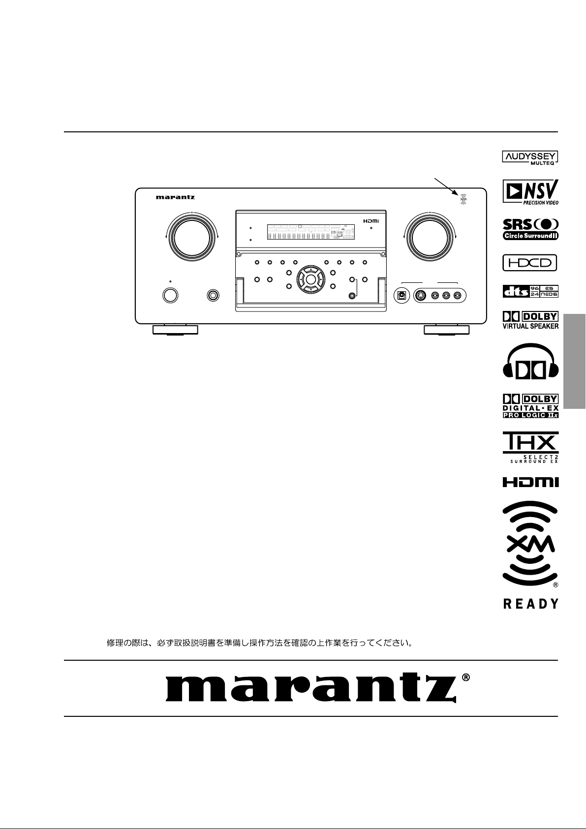
AVSURROUND RECEIVER SR8001
PHONES
PUREDIRECT
DSD
PUREDIRECT THX
SURROUND
MODE AUTO
SURR DIRECT
SLEEP
AUTO
MULTI
7.1CHINPUT
MULTI
SPEAKER
MENU
V-OFFDISP MULTI AUTO TUNED ST SPKRAB
PEAK ANALOG
DISC6.1 MTX 6.1 EQ
NIGHT
ENTER
ATT
DIGITAL
AAC
PCM
BAND
T-MODE
DISPLAY
EXIT
TABLE OF CONTENTS
AV Surround Receiver
/U Only
READY
UP
RLVIDEO
AUDIO
SURROUND
DIGITAL
LCR
LFE
SL S SR
MEMORY CLEAR
MultEQ
MIC
SPEAKERS
VOLUME
DOWN
A/B
AUX1 INPUT
DIGITAL
S-VIDEO
Please use this service manual with referring to the user guide ( D.F.U. ) without fail.
SR8001
Part no. 90M06CW855010
First Issue 2006.08
MZ
Page 2
MARANTZ DESIGN AND SERVICE
Using superior design and selected high grade components,
Only original
MARANTZ
parts can insure that your
MARANTZ
MARANTZ
product will continue to perform to the specifi cations for which
company has created the ultimate in stereo sound.
it is famous.
Parts for your
MARANTZ
ORDERING PARTS :
equipment are generally available to our National Marantz Subsidiary or Agent.
Parts can be ordered either by mail or by Fax.. In both cases, the correct part number has to be specifi ed.
The following information must be supplied to eliminate delays in processing your order :
1. Complete address
2. Complete part numbers and quantities required
3. Description of parts
4. Model number for which part is required
5. Way of shipment
6. Signature : any order form or Fax. must be signed, otherwise such part order will be considered as null and void.
USA
MARANTZ AMERICA, INC
100 CORPORATE DRIVE
MAHWAH, NEW JERSEY 07430
USA
AUSTRALIA
QualiFi Pty Ltd,
24 LIONEL ROAD,
MT. WAVERLEY VIC 3149
AUSTRALIA
PHONE : +61 - (0)3 - 9543 - 1522
FAX : +61 - (0)3 - 9543 - 3677
EUROPE / TRADING
MARANTZ EUROPE B.V.
P. O. BOX 8744, BUILDING SILVERPOINT
BEEMDSTRAAT 11, 5653 MA EINDHOVEN
THE NETHERLANDS
PHONE : +31 - 40 - 2507844
FAX : +31 - 40 - 2507860
THAILAND
MRZ STANDARD CO., LTD
746 - 754 MAHACHAI ROAD.,
WANGBURAPAPIROM, PHRANAKORN,
BANGKOK, 10200 THAILAND
PHONE : +66 - 2 - 222 9181
FAX : +66 - 2 - 224 6795
CANADA
MARANTZ CANADA INC.
5-505 APPLE CREEK BLVD.
MARKHAM, ONTARIO L3R 5B1
CANADA
PHONE : 905 - 415 - 9292
FAX : 905 - 475 - 4159
SINGAPORE
WO KEE HONG DISTRIBUTION PTE LTD
No.1 JALAN KILANG TIMOR
#08-03 PACIFIC TECH CENTRE
SINGAPORE 159303
PHONE : +65 6376 0338
FAX : +65 6376 0166
NEW ZEALAND
WILDASH AUDIO SYSTEMS NZ
14 MALVERN ROAD MT ALBERT
AUCKLAND NEW ZEALAND
PHONE : +64-9-8451958
FAX :+64-9-8463554
JAPAN
D&M Holdings Inc.
D&M BUILDING, 2-1 NISSHIN-CHO,
KAWASAKI-KU, KAWASAKI-SHI,
KANAGAWA, 210-8569 JAPAN
TAIWAN
PAI- YUING CO., LTD.
6 TH FL NO, 148 SUNG KIANG ROAD,
TAIPEI, 10429, TAIWAN R.O.C.
PHONE : +886 - 2 - 25221304
FAX : +886 - 2 - 25630415
MALAYSIA
WO KEE HONG ELECTRONICS SDN. BHD.
2ND FLOOR BANGUNAN INFINITE CENTRE
LOT 1, JALAN 13/6, 46200 PETALING JAYA
SELANGOR DARUL EHSAN, MALAYSIA
PHONE : +60 - 3 - 7954 8088
FAX :+60-3-79547088
KOREA
MARANTZ KOREA CO., LTD.
ROOM 604, ELECTRO OFFICE, 16-58,
HANGGANG-RO 3GA, YONGSAN-KU,
SEOUL, 140-013, KOREA
PHONE : +82 - 2 - 323 - 2155
FAX : +82 - 2 - 323 - 2154
CHINA
MARANTZ SHANGHAI TRADING LTD.
ROOM.506 SHANGHAI LIGHT INDUSTRY MANSION
1578 NANJING (WEST) ROAD SHANGHAI
CHINA
TEL : 021 - 6248 - 1064
FAX : 021 - 6248 - 3565
SHOCK, FIRE HAZARD SERVICE TEST :
CAUTION : After servicing this appliance and prior to returning to customer, measure the resistance between either primary AC
cord connector pins ( with unit NOT connected to AC mains and its Power s witch ON ), and the face or Front P anel of product an d
controls and chassis bottom.
Any resistance measurement less than 1 Megohms should cause unit to be repaired or corrected before A C po wer is applied, and
verifi ed before it is return to the user/customer.
Ref. UL Standard No. 1492.
In case of diffi culties, do not hesitate to contact the Technical
Department at above mentioned address.
060607MZ
Page 3
1. TECHNICAL SPECIFICATIONS
DIG
L
R
L
V
O
S
O
A
O
E
UPDO
S
PHONES
I
AV S
Q
ENTER
MENUPU
MO
O
MULTI
T-MO
Y
EXIT
S
S
C
PU
SURROUND
S
R
MULTI
DSD
C
SL S SR
S
LFE
SURROUND
DISP
MULTIAUTO
TUNEDSTS
NIG
PEAK
OG
ATT
S
SURR DIRECT
AUTODISC 6.1
MTX 6.1
Q
PCM
A
.
)
)
)
3
6
i
s.
)
8i
s
)
)
/
i
s
FM TUNER SECTION
Frequency Range ......................87.5 - 108.0 MHz [ /K /N /U ]
Usable Sensitivity ..................................IHF 1.8 µV/16.4 dBf
Signal to Noise Ratio ..........................Mono/Stereo 75/70 dB
Distortion ...........................................Mono/Stereo 0.2/0.3 %
Stereo Separation ............................................... 1 kHz 45 dB
Alternate Channel Selectivity ......................± 300 kHz 60 dB
Image Rejection ...............................................98 MHz 70 dB
Tuner Output Level ..................1 kHz, ± 75 kHz Dev 800 mV
AM TUNER SECTION
Frequency Range ............................. 531 - 1602 kHz [ /K /N ]
..................................520 - 1710 kHz [ /U ]
Signal to Noise Ratio .................................................... 50 dB
Usable Sensitivity .............................................. Loop 400 µV
Distortion ........................................400Hz, 30 % Mod. 0.5 %
Selectivity ......................................................± 20 kHz 70 dB
HDMI SECTION
Version ...........................................................1.2 [INPUT]
.......................................................1.1 [OUTPUT]
AUDIO SECTION
Power Output (20 Hz - 20 kHz/THD=0.08%)
Front L&R ................................................8 ohms 125 W / Ch
Center ......................................................8 ohms 125 W / Ch
Surround L&R ..........................................8 ohms 125 W / Ch
Surround Back L&R .................................8 ohms 125 W / Ch
Front L&R ................................................6 ohms 160 W / Ch
Center ......................................................6 ohms 160 W / Ch
Surround L&R ..........................................6 ohms 160 W / Ch
Surround Back L&R .................................6 ohms 160 W / Ch
Input Sensitivity/Impedance ......................168 mV/ 47 kohms
Signal to Noise Ratio
(Analog Input / Pure Direct) ................................. 105 dB
Frequency Response
(Analog Input / Pure Direct) ........8 Hz - 100 kHz (± 3 dB)
(Digital Input / 96 kHz PCM) .........8 Hz - 45 kHz (± 3 dB)
VIDEO SECTION
Television Format ..................................................NTSC/PAL
Input Level/Impedance ..................................1 Vp-p/75 ohms
Output Level/Impedance ................................1 Vp-p/75 ohms
Video Frequency Response ..............5 Hz to 8 MHz (- 1 dB)
Video Frequency (Component) .......5 Hz to 80 MHz (- 1 dB)
S/N ................................................................................ 60 dB
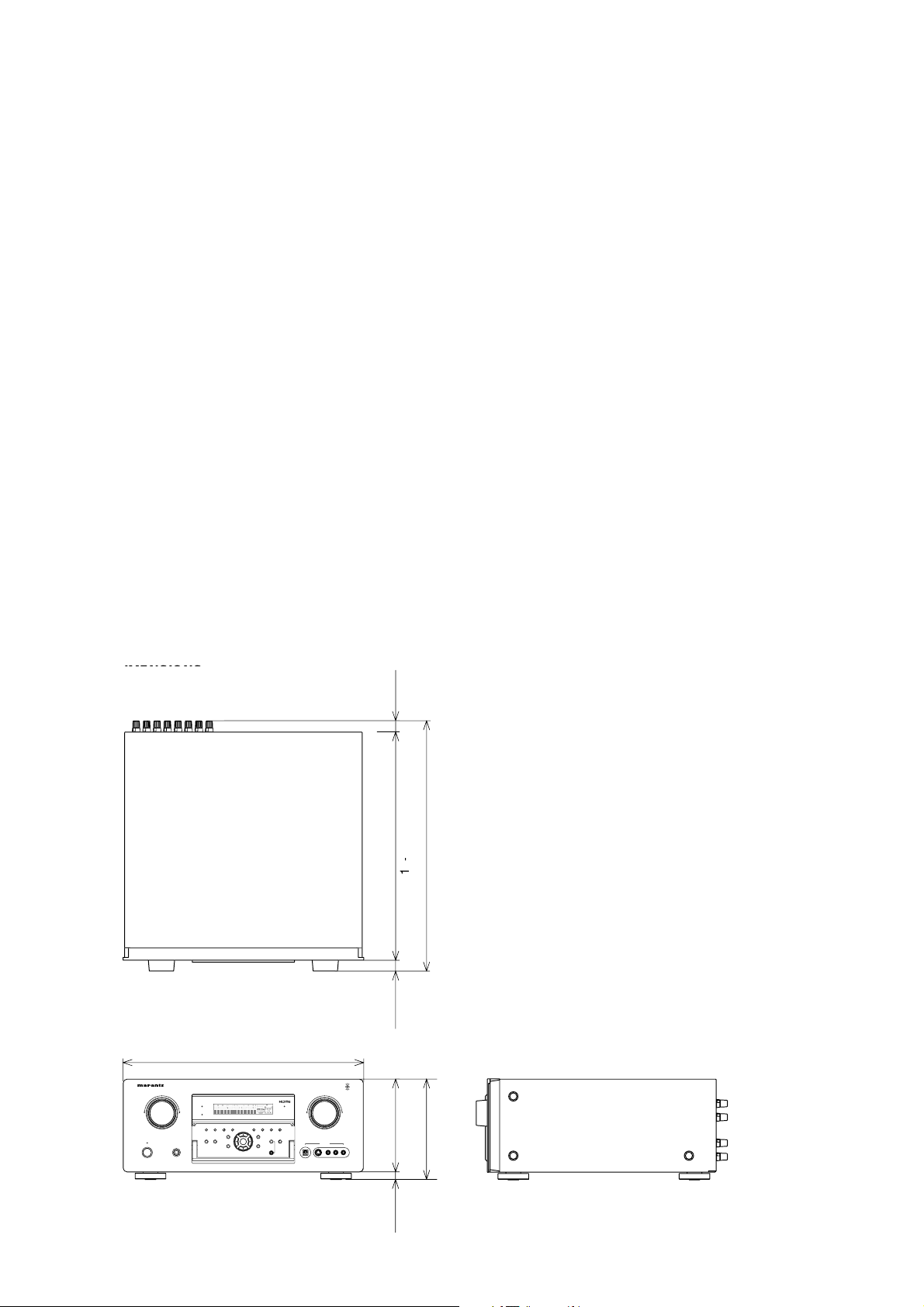
DIMENSIONS
17-5/16 ins. (440 mm
URROUND RECEIVER SR8001
NPUT SELECTOR
TANDBY
POWER ON/STANDBY
n
7/
22 mm
GENERAL
Power Requirement ..............................AC 220 V 50 Hz [ /K ]
.........................AC 230 V 50/60 Hz [ /N ]
..............................AC 120 V 60 Hz [ /U ]
Power Consumption ............................................790 W [ /N ]
..............................................6.5 A [ /U ]
Weight .......................................................15.0 kg (33.1 lbs)
n
354 mm
(396 mm)
3-15/16 ins
ACCESSORIES
Remote Control Unit RC8001SR ..........................................1
AAA-size batteries ............................................................... 2
Microphone ...........................................................................1
FM Antenna ..........................................................................1
AM Loop Antenna .................................................................1
Front AUX Jack Cover ..........................................................1
n
/1
20 mm
1
READY
RE DIRECT
V-OFF
PKR A B
ANAL
DIGITAL
DIGITAL
HT
LEEP
E
AC
MEMORYCLEAR
PEAKE
DE
7.1CH INPUT
DISPLA
MultE
MI
RE DIRECTTHX
DE AUT
VOLUM
WN
PEAKER
A/B
UX 1 INPUT
ITA
IDE
-VIDE
AUDI
-1/4 ins
6-3/4 ins.
(170 mm
184 mm
AC cable ...............................................................................1
/16 ins.
14 mm)
1
Page 4
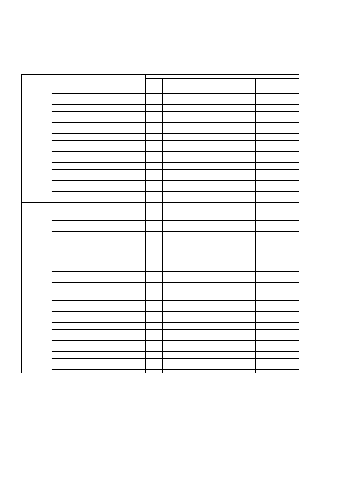
The relation between the selected surround mode and the input signal
The surround mode is selected with the surround mode buttons on SR7001/SR8001 or the remote control unit. However,
the sound you hear is subject to the relationship between the selected surround mode and input signal. That relationship is
as follows;
Surround Mode Input Signal Decoding
AUTO
SOURCE DIRECT
PURE DIRECT
EX/ES
DOLBY
(PLIIx movie)
(PLIIx music)
(PLIIx game)
DTS
(Neo:6 Cinema)
(Neo:6 Music)
CSII Cinema
CSII Music
CSII Mono
STEREO
Dolby Surr.EX Dolby Digital EX
Dolby D (5.1ch) Dolby Digital 5.1
Dolby D (2ch) Dolby Digital 2.0
Dolby D (2ch Surr) Pro Logic IIx movie
DTS-ES DTS-ES
DTS 96/24 DTS-96/24
DTS (5.1ch) DTS 5.1
Multi Ch-PCM Multi Ch-PCM
Multi Ch-PCM 96kHz Multi Ch-PCM 96kHz
SA-CD (5.1ch) Multi Ch-PCM
SA-CD (2ch) PCM (Stereo)
PCM (Audio) PCM (Stereo)
PCM 96kHz PCM (Stereo 96kHz)
HDCD HDCD
Analog Stereo
7.1ch input Multi Ch
Dolby Surr.EX Dolby Digital EX
Dolby D (5.1ch) Dolby Digital 5.1
Dolby D (2ch) Dolby Digital 2.0
Dolby D (2ch Surr) Pro Logic IIx movie
DTS-ES DTS-ES
DTS 96/24 DTS-96/24
DTS (5.1ch) DTS 5.1
Multi Ch-PCM Multi Ch-PCM
Multi Ch-PCM 96kHz Multi Ch-PCM 96kHz
SA-CD (5.1ch) SA-CD (5.1ch)
SA-CD (2ch) SA-CD (2ch)
PCM (Audio) PCM (Stereo)
PCM 96kHz PCM (Stereo 96kHz)
HDCD HDCD
Analog Stereo
7.1ch input Multi Ch
Dolby Surr.EX Dolby Digital EX
Dolby D (5.1ch) Dolby Digital EX
DTS-ES DTS-ES
DTS (5.1ch) DTS-ES
Multi-PCM Multi Ch-PCM + Dolby EX
SA-CD (5.1ch) Multi Ch-PCM + Dolby EX
Dolby Surr.EX Dolby Digital 5.1
Dolby D (5.1ch) Dolby Digital 5.1
Dolby D (5.1ch) Dolby Digital 5.1 + PLIIx
Dolby D (2ch) Pro Logic IIx
Dolby D (2ch Surr) Pro Logic IIx
Multi Ch-PCM Multi Ch-PCM + PLII x
SA-CD (5.1ch) Multi Ch-PCM + PLIIx
SA-CD (2ch) Pro Logic IIx
PCM (Audio) Pro Logic IIx
HDCD Pro Logic IIx
Analog Pro Logic IIx
DTS-ES DTS 5.1
DTS 96/24 DTS-96/24
DTS (5.1ch) DTS 5.1
Dolby D (2ch) Neo:6
Dolby D (2ch Surr) Neo:6
SA-CD (2ch) Neo:6
PCM(Audio) Neo:6
HDCD Neo:6
Analog Neo:6
Dolby D (2ch) CSII
Dolby D (2ch Surr) CSII
SA-CD (2ch) CSII
PCM(Audio) CSII
HDCD CSII
Analog CSII
Dolby Surr.EX Stereo
Dolby D (5.1ch) Stereo
Dolby D (2ch) Stereo
Dolby D (2ch Surr) Stereo
DTS-ES Stereo
DTS 96/24 Stereo
DTS (5.1ch) Stereo
Multi Ch-PCM Stereo
Multi Ch-PCM 96kHz Stereo
SA-CD (5.1ch) Stereo
SA-CD (2ch) Stereo
PCM (Audio) Stereo
PCM 96kHz Stereo
HDCD Stereo
Analog Stereo
Output Channel Front information display
SLSRSBL
L/R C
OOOOO
OOO-O
O
---
OOOOO
OOOOO
OOO-O
OOO-O
OOO-O
OOO-O
OOO-O
O
---OSA-CD L, R
O
---OPCM L, R
O
---OPCM L, R
O
---OPCM, HDCD L, R
O
---OANALOG -
OOOOO
OOOOO
OOO-O
O
---
OOOOO
OOOOO
OOO-O
OOO-O
OOO-O
OOO-O
OOO-O
O
---OSA-CD L, R
O
----PCM L, R
O
----PCM L, R
O
- - - - PCM, HDCD L, R
O
- - - - ANALOG -
OOOOO
OOOOO
OOOOO
OOOOO
OOOOO
OOOOO
OOOOO
OOO-O
OOO-O
OOOOO
OOOOO
OOOOO
OOOOO
OOOOO
OOOOO
OOOOO
OOOOO
OOOOO
OOO-O
OOO-O
OOO-O
OOOOO
OOOOO
OOOOO
OOOOO
OOOOO
OOOOO
OOOOO
OOOOO
OOOOO
OOOOO
OOOOO
OOOOO
O
---
O
---
O
---
O
---
O
---Odts, ES L, C, R, SL, SR, S, LFE
O
---Odts 96/24 L, C, R, SL, SR, LFE
O
---Odts L, C, R, SL, SR, LFE
O
---OM-PCM L, C, R, SL, SR, LFE
O
---OM-PCM L, C, R, SL, SR, LFE
O
---OSA-CD L, C, R, SL, SR, LFE
O
---OSA-CD L, R
O
---OPCM L, R
O
---OPCM L, R
O
---OPCM, HDCD L, R
O
---OANALOG -
SBR
SubW
Signal format indicators Channel status
2 DIGITAL EX
2 DIGITAL
O
2 DIGITAL
2 DIGITAL 2 SURROUND
dts, ES L, C, R, SL, SR, S, LFE
dts 96/24 L, C, R, SL, SR, LFE
dts L, C, R, SL, SR, LFE
M-PCM L, C, R, SL, SR, LFE
M-PCM L, C, R, SL, SR, LFE
SA-CD L, C, R, SL, SR, LFE
ANALOG -
2 DIGITAL EX
2 DIGITAL
O
2 DIGITAL
2 DIGITAL 2 SURROUND
dts, ES L, C, R, SL, SR, S, LFE
dts 96/24 L, C, R, SL, SR, LFE
dts L, C, R, SL, SR, LFE
M-PCM L, C, R, SL, SR, LFE
M-PCM L, C, R, SL, SR, LFE
SA-CD L, C, R, SL, SR, LFE
ANALOG -
2 DIGITAL EX
2 DIGITAL
dts, ES L, C, R, SL, SR, S, LFE
dts L, C, R, SL, SR, LFE
M-PCM L, C, R, SL, SR, LFE
SA-CD L, C, R, SL, SR, LFE
2 DIGITAL EX
2 DIGITAL
2 DIGITAL
2 DIGITAL
2 DIGITAL 2 SURROUND
M-PCM L, C, R, SL, SR, LFE
SA-CD L, C, R, SL, SR, LFE
SA-CD L, R
PCM L, R
PCM, HDCD L, R
ANALOG dts, ES L, C, R, SL, SR, S, LFE
dts 96/24 L, C, R, SL, SR, LFE
dts L, C, R, SL, SR, LFE
2 DIGITAL
2 DIGITAL 2 SURROUND
SA-CD L, R
PCM L, R
PCM, HDCD L, R
ANALOG -
2 DIGITAL
2 DIGITAL 2 SURROUND
SA-CD L, R
PCM L, R
PCM, HDCD L, R
ANALOG -
O
2 DIGITAL EX
O
2 DIGITAL
O
2 DIGITAL
O
2 DIGITAL 2 SURROUND
L, C, R, SL, SR, S, LFE
L, C, R, SL, SR, LFE
L, R
L, R, S
L, C, R, SL, SR, S, LFE
L, C, R, SL, SR, LFE
L, R
L, R, S
L, C, R, SL, SR, S, LFE
L, C, R, SL, SR, LFE
L, C, R, SL, SR, S, LFE
L, C, R, SL, SR, LFE
L, C, R, SL, SR, LFE
L, R
L, R, S
L, R
L, R, S
L, R
L, R, S
L, C, R, SL, SR, S, LFE
L, C, R, SL, SR, LFE
L, R
L, R, S
2
Page 5
Surround Mode Input Signal Decoding
Dolby Virtual
Speaker
Multi Ch.
Stereo
Dolby H.P Dolby Surr.EX Dolby H.P
THX
(THX Games)
THX Select2
(THX EX)
(THX Music)
(THX Games)
Dolby Surr.EX Dolby Virtual Speaker
Dolby D (5.1ch) Dolby Virtual Speaker
Dolby D (2ch) Dolby Virtual Speaker
Dolby D (2ch Surr) Dolby Virtual Speaker
DTS-ES Dolby Virtual Speaker
DTS 96/24 Dolby Virtual Speaker
DTS (5.1ch) Dolby Virtual Speaker
Multi Ch-PCM Dolby Virtual Speaker
SA-CD (5.1ch) Dolby Virtual Speaker
SA-CD (2ch) Dolby Virtual Speaker
PCM (Audio) Dolby Virtual Speaker
HDCD Dolby Virtual Speaker
Analog Dolby Virtual Speaker
Dolby Surr.EX Dolby Digital EX
Dolby D (5.1ch) Dolby Digital 5.1
Dolby D (2ch) Multi Channel Stereo
Dolby D (2ch Surr) Multi Channel Stereo
DTS-ES DTS-ES
DTS 96/24 DTS-96/24
DTS (5.1ch) DTS 5.1
Multi Ch-PCM Multi Ch-PCM
Multi Ch-PCM 96kHz Multi Ch-PCM 96kHz
SA-CD (5.1ch) Multi Ch-PCM
SA-CD (2ch) Multi Channel Stereo
PCM (Audio) Multi Channel Stereo
HDCD Multi Channel Stereo
Analog Multi Channel Stereo
Dolby D (5.1ch) Dolby H.P
Dolby D (2ch) Dolby H.P
Dolby D (2ch Surr) Dolby H.P
DTS-ES Dolby H.P
DTS 96/24 Dolby H.P
DTS (5.1ch) Dolby H.P
Multi Ch-PCM Dolby H.P
SA-CD (5.1ch) Dolby H.P
SA-CD (2ch) Dolby H.P
PCM (Audio) Dolby H.P
HDCD Dolby H.P
Analog Dolby H.P
Dolby Surr.EX Dolby Digital + THX Surround EX
Dolby D (5.1ch) Dolby Digital 5.1+ THX 5.1
Dolby D (2ch) Pro Logic IIx movie + THX
Dolby D (2ch Surr) Pro Logic IIx movie + THX
DTS-ES DTS-ES + THX
DTS (5.1ch) DTS + THX 5.1
Multi Ch-PCM Multi Ch-PCM + THX5.1
SA-CD (5.1ch) Multi Ch-PCM + THX5.1
SA-CD (2ch) Pro Logic IIx movie + THX
PCM (Audio) Pro Logic IIx movie + THX
HDCD Pro Logic IIx movie + THX
Analog Pro Logic IIx movie + THX
Dolby Surr.EX Dolby Digital + THX Surround EX
Dolby D (5.1ch) Dolby Digital 5.1+ THX Select2 Cinema
Dolby D (2ch) Pro Logic IIx movie + THX
Dolby D (2ch Surr) Pro Logic IIx movie + THX
DTS-ES DTS-ES + THX
DTS (5.1ch) DTS + THX Select2 Cinema
Multi Ch-PCM Multi Ch-PCM + THX Select2 Cinema
SA-CD (5.1ch) Multi Ch-PCM + THX Select2 Cinema
SA-CD (2ch) Pro Logic IIx movie + THX
PCM (Audio) Pro Logic IIx movie + THX
HDCD Pro Logic IIx movie + THX
Analog Pro Logic IIx movie + THX
Output Channel Front information display
L/R C
O
O
O
O
O
O
O
O
O
O
O
O
O
OOOOO
OOO-O
OOOOO
OOOOO
OOOOO
OOO-O
OOO-O
OOO-O
OOO-O
OOO-O
OOOOO
OOOOO
OOOOO
OOOOO
O
O
O
O
O
O
O
O
O
O
O
O
O
OOOOO
OOO-O
OOOOO
OOOOO
OOOOO
OOO-O
OOO-O
OOO-O
OOOOO
OOOOO
OOOOO
OOOOO
OOOOO
OOOOO
OOOOO
OOOOO
OOOOO
OOOOO
OOOOO
OOOOO
OOOOO
OOOOO
OOOOO
OOOOO
SLSRSBL
SubW
Signal format indicators Channel status
SBR
----
----
----
----
- - - - dts, ES L, C, R, SL, SR, S, LFE
- - - - dts 96/24 L, C, R, SL, SR, LFE
- - - - dts L, C, R, SL, SR, LFE
- - - - M-PCM L, C, R, SL, SR, LFE
- - - - SA-CD L, C, R, SL, SR, LFE
----SA-CD L, R
----PCM L, R
- - - - PCM, HDCD L, R
----ANALOG -
----
----
----
----
- - - - dts, ES L, C, R, SL, SR, S, LFE
- - - - dts 96/24 L, C, R, SL, SR, LFE
- - - - dts L, C, R, SL, SR, LFE
- - - - M-PCM L, C, R, SL, SR, LFE
- - - - SA-CD L, C, R, SL, SR, LFE
----SA-CD L, R
----PCM L, R
- - - - PCM, HDCD L, R
----ANALOG -
2 DIGITAL EX
2 DIGITAL
2 DIGITAL
2 DIGITAL 2 SURROUND
2 DIGITAL EX
2 DIGITAL
2 DIGITAL
2 DIGITAL 2 SURROUND
dts, ES L, C, R, SL, SR, S, LFE
dts 96/24 L, C, R, SL, SR, LFE
dts L, C, R, SL, SR, LFE
M-PCM L, C, R, SL, SR, LFE
M-PCM L, C, R, SL, SR, LFE
SA-CD L, C, R, SL, SR, LFE
SA-CD L, R
PCM L, R
PCM, HDCD L, R
ANALOG -
2 DIGITAL EX
2 DIGITAL
2 DIGITAL
2 DIGITAL 2 SURROUND
2 DIGITAL EX
2 DIGITAL
2 DIGITAL
2 DIGITAL 2 SURROUND
dts, ES L, C, R, SL, SR, S, LFE
dts L, C, R, SL, SR, LFE
M-PCM L, C, R, SL, SR, LFE
SA-CD L, C, R, SL, SR, LFE
SA-CD L, R
PCM L, R
PCM, HDCD L, R
ANALOG -
2 DIGITAL EX
2 DIGITAL
2 DIGITAL
2 DIGITAL 2 SURROUND
dts, ES L, C, R, SL, SR, S, LFE
dts L, C, R, SL, SR, LFE
M-PCM L, C, R, SL, SR, LFE
SA-CD L, C, R, SL, SR, LFE
SA-CD L, R
PCM L, R
PCM, HDCD L, R
ANALOG -
L, C, R, SL, SR, S, LFE
L, C, R, SL, SR, LFE
L, R
L, R, S
L, C, R, SL, SR, S, LFE
L, C, R, SL, SR, LFE
L, R
L, R, S
L, C, R, SL, SR, S, LFE
L, C, R, SL, SR, LFE
L, R
L, R, S
L, C, R, SL, SR, S, LFE
L, C, R, SL, SR, LFE
L, R
L, R, S
L, C, R, SL, SR, S, LFE
L, C, R, SL, SR, LFE
L, R
L, R, S
Notes:
• Dolby Digital (2 channel L/R): Speakers for signal
with Dolby Surround are fully equipped.
• No sound is outputs from the surround speaker,
center speaker and subwoofer if the DVD disc has
no surround data.
Abbreviations
L/R : Front speakers
C : Center speaker
SL/SR : Surround speakers
SBL/SBR : Surround back speakers
SubW : Subwoofer
3
Page 6

2. TECHNICAL DESCRIPTION
DESCRIPTION
THX® is an exclusive set of standards and
technologies established by the world-renowned fi lm
production company, Lucasfi lm Ltd. THX resulted
from George Lucas’ desire to reproduce the movie
soundtrack as faithfully as possible both in the movie
theater and in the home theater.
THX engineers developed patented technologies to
accurately translate the sound from a movie theater
environment into the home, correcting the tonal and
spatial errors that occur.
When the THX mode of the SR7001 is on, three
distinct THX technologies are automatically added:
Re-Equalization-restores the correct tonal balance
for watching a movie in a home environment.
These sounds are otherwise mixed to be brighter
for a large movie theater. Re-EQ compensates for
this and prevents the soundtracks from being overly
bright and harsh when played in a home theater.
Timbre Matching-fi lters the information going to the
surround speakers so they more closely match the
tonal characteristics of the sound coming from the
front speakers.
This ensures seamless panning between the front
and surround speakers.
Adaptive Decorrelation-slightly changes one
surround channel’s time and phase relationship with
respect to the other surround channel.
This expands the listening position and creates with
only two surround speakers the same spacious
surround experience as in a movie theater with
multiple surround speakers.
The Marantz SR7001 was required to pass a rigorous
series of quality and performance tests, in addition to
incorporating the technologies explained above, in
order to be THX certifi ed by Lucasfi lm Ltd.
THX requirements cover every aspect of performance
including pre-amplifier and power amplifier
performance and operation, and hundreds of other
parameters in both the digital and analog domain.
Movies which have been encoded in Dolby Digital,
DTS, Dolby Pro Logic, stereo and Mono will all
benefi t from the THX mode when being viewed.
The THX mode should only be activated when
watching movies which were originally produced for
a movie theater environment.
THX need not be activated for music, movies
made especially for TV, or shows such as sports
programming, talk shows, etc.
This is because they were originally mixed for a small
room environment.
THX and Select 2 are trademarks of THX Ltd. THX
may be registered in some jurisdictions. Surround
EX is a trademark of Dolby Laboratories. Used with
permission.
THX Surround EX—Dolby DIgital Surround EX is a
joint development of Dolby Laboratories and THX
Ltd.
In a movie theater, fi lm soundtracks that have been
encoded with Dolby Digital Surround EX technology
are able to reproduce an extra channel which has
been added during the mixing of the program. This
channel, called Surround Back, places sounds
behind the listener in addition to the currently
available front left, front center, front right, surround
right, surround left and subwoofer channels. This
additional channel provides the opportunity for more
detailed imaging behind the listener and brings more
depth, spacious ambience and sound localization
than ever before.
Movies that were created using the Dolby Digital
Surround EX technology, when released into the
home consumer market may exhibit wording to that
effect on the packaging. A list of movies created
using this technology can be found on the Dolby
web site at www.dolby.com. A list of available DVD
software titles encoded with this technology an be
found at www.thx.com.
Only receiver and controller products bearing the
THX Surround EX logo, when in the THX Surround
EX mode, faithfully reproduce this new technology
in the home. This product may also engage the
THX Surround EX mode during the playback of 5.1
channel material that is not Dolby Digital Surround
EX eocnded. In such case, the information delivered
to the Surround Back channel will be program
dependent and may or may not be very pleasing
depending on the particular soundtrack and the
tastes of the individual listener.
“SURROUND EX™” is a trademark of Dolby
Laboratories. Used under authorization.
4
Page 7

THX Select2
Before any home theater component can be THX
Select2 certifi ed, it must pass a rigorous series of
quality and performance tests. Only then can a
product feature the THX Select2 logo, which is your
guarantee that the Home Theater products you
purchase will give you superb performance for many
years to come. THX Select2 requirements defi ne
hundreds of parameters, including power amplifi er
performance, and pre-amplifi er performance and
operation for both digital and analog domains. THX
Select2 receivers also feature proprietary THX
technologies
(e.g., THX Mode) which accurately translate movie
soundtracks for home theater playback.
DTS was introduced in 1994 to provide 5.1 channels
of discrete digital audio into home theater systems.
DTS brings you premium quality discrete multichannel
digital sound to both movies and music.
DTS is a multichannel sound system designed to
create full range digital sound reproduction.
The no compromise DTS digital process sets the
standard of quality for cinema sound by delivering
an exact copy of the studio master recordings to
neighborhood and home theaters.
Now, every moviegoer can hear the sound exactly as
the moviemaker intended.
DTS can be enjoyed in the home for either movies or
music on of DVD’s, LD’s, and CD’s.
“DTS” and “DTS Digital Surround” are registered
trademarks of Digital Theater Systems, Inc.
Neo:6 offers several important improvements as
follow,
• Neo:6 provides up to six full-band channels of
matrix decoding from stereo matrix material. Users
with 6.1 and 5.1 systems will derive six and fi ve
separate channels, respectively, corresponding to
the standard home-theater speaker layouts.
• Neo:6 technology allows various sound elements
within a channel or channels to be steered
separately, and in a way which follows naturally
from the original presentation.
• Neo:6 offers a music mode to expand stereo
nonmatrix recordings into the fi ve- or six-channel
layout, in a way which does not diminish the subtlety
and integrity of the original stereo recording.
DTS-ES Extended Surround is a new multichannel
digital signal format developed by Digital Theater
Systems Inc. While offering high compatibility with
the conventional DTS Digital Surround format, DTSES Extended Surround greatly improves the 360degree surround impression and space expression
thanks to further expanded surround signals. This
format has been used professionally in movie
theaters since 1999.
In addition to the 5.1 surround channels (FL, FR, C,
SL, SR and LFE), DTS-ES Extended Surround also
offers the SB (Surround Back) channel for surround
playback with a total of 6.1 channels. DTS-ES
Extended Surround includes two signal formats with
different surround signal recording methods, as DTSES Discrete 6.1 and DTS-ES Matrix 6.1.
“DTS”, “DTS-ES and “Neo:6” are trademarks of
Digital Theater Systems, Inc.
The advantages of discrete multichannel systems
over matrix are well known.
But even in homes equipped for discrete multichannel,
there remains a need for high-quality matrix decoding.
This is because of the large library of matrix surround
motion pictures available on disc and on VHS tape;
and analog television broadcasts.
The typical matrix decoder of today derives a center
channel and a mono surround channel from twochannel matrix stereo material. It is better than a
simple matrix in that it includes steering logic to
improve separation, but because of its mono, bandlimited surround it can be disappointing to users
accustomed to discrete multichannel.
The stereo CD is a 16-bit medium with sampling at
44.1 kHz. Professional audio has been 20- or 24-
bit for some time, and there is increasing interest
in higher sampling rates both for recording and for
delivery into the home. Greater bit depths provide
extended dynamic range. Higher sampling rates
allow wider frequency response and the use of antialias and reconstruction fi lters with more favorable
aural characteristics.
DTS 96/24 allows for 5.1channel sound tracks to be
encoded at a rate of 96kHz/24bits on DVD-Video
titles.
5
Page 8

When DVD-video appeared, it became possible to
deliver 24-bit, 96 kHz audio into the home, but only in
two channels, and with serious limitations on picture.
This capability has had little use.
DVD-audio allows 96/24 in six channels, but a
new player is needed, and only analog outputs are
provided, necessitating the use of the D/A converters
and analog electronics provided in the player.
DTS 96/24 offers the following:
1. Sound quality transparent to the original 96/24
master.
2. Full backward compatibility with all existing
decoders. (Existing decoders will output a 48 kHz
signal)
3. No new player required: DTS 96/24 can be carried
on DVD-video, or in the video zone of DVD-audio,
accessible to all DVD players.
4. 96/24 5.1-channel sound with full-quality fullmotion video, for music programs and motion
picture soundtracks on DVD-video.
“DTS” and “DTS 96/24” are trademarks of Digital
Theater Systems, Inc.
Dolby Digital EX creates six full-bandwidth output
channels from 5.1-channel sources. This is done
using a matrix decoder that derives three surround
channels from the two in the original recording. For
best results, Dolby Digital EX should be used with
movies soundtracks recorded with Dolby Digital
Surround EX.
About Dolby Pro Logic IIx
Dolby Pro Logic II x technology delivers a natural
and immersing 7.1-channel listening experience
to the home theater environment. A product of
Dolby's expertise in surround sound and matrix
decoding technologies, Dolby Pro Logic II x is a
complete surround sound solution that maximizes
the entertainment experience from stereo as well as
5.1-channel encoded sources.
Dolby Pro Logic II x is fully compatible with Dolby
Surround Pro Logic technology and can optimally
decode the thousands of commercially available
Dolby Surround encoded video cassettes and
television programs with enhanced depth and
spatiality. It can also process any high-quality
stereo or Advanced Resolution 5.1-channel music
content into a seamless 6.1- or 7.1-channel listening
experience.
Dolby Digital identifi es the use of Dolby Digital audio
coding for such consumer formats as DVD and DTV.
As with fi lm sound, Dolby Digital can provide up
to fi ve full-range channels for left, center, and right
screen channels, independent left and right surround
channels, and a sixth (“.1”) channel for low-frequency
effects.
Dolby Surround Pro Logic
II
is an improved matrix
decoding technology that provides better spatiality
and directionality on Dolby Surround program
material; provides a convincing three-dimensional
soundfi eld on conventional stereo music recordings;
and is ideally suited to bring the surround experience
to automotive sound. While conventional surround
programming is fully compatible with Dolby Surround
Pro Logic
II
decoders, soundtracks will be able to be
encoded specifi cally to take full advantage of Pro
Logic
II
playback, including separate left and right
surround channels. (Such material is also compatible
with conventional Pro Logic decoders.)
The Dolby Headphone technology provides a
surround sound listening experience over headphones.
When listening to multichannel content such as DVD
movies over headphones, the listening experience
is fundamentally different than listening to speakers.
Since the headphone speaker drivers are covering
the pinna of the ear, the listening experience differs
greatly from traditional speaker playback. Dolby
utilizes patented headphone perspective curves to
solve this problem and provides a non-fatiguing,
immersive, home theater listening experience. Dolby
Headphone also delivers exceptional 3D audio from
stereo material.
6
Page 9

Dolby Virtual Speaker is a technologycertified
by Dolby Laboratories that creates a virtualized
surround sound experience from two speakers using
a multichannel Dolby Digital source. Additionally,
Dolby Virtual Speaker can simulate the surround
sound effect produced by Dolby Pro Logic or Dolby
Pro Logic II .
Dolby Virtual Speaker retains all the original
Multichannel audio information and provides the
listener with the sensation of being surrounded by
additional speakers.
Manufactured under license from Dolby Laboratories.
“Dolby”, “Pro Logic”, “Surround EX”, and the doubleD symbol are trademarks of Dolby Laboratories.
Circle Surround II (CS-II ) is a powerful and versatile
multichannel technology. CS-II is designed to enable
up to 6.1 multichannel surround sound playback
from mono, stereo, CS encoded sources and other
matrix encoded sources. In all cases the decoder
extends it into 6 channels of surround audio and a
LFE/subwoofer signal. The CS-II decoder creates a
listening environment that places the listener “inside”
music performances and dramatically improves
both hi-fi audio conventional surround-encoded
video material. CS-II provides composite stereo rear
channels to greatly improve separation and image
positioning– adding a heightened sense of realism to
both audio and A/V productions.
CS-II is packed with other useful feature like dialog
clarity (SRS Dialog) for movies and cinema-like bass
enrichment (TruBass). CS-II can enable the dialog
to become clearer and more discernable in movies
and it enables the bass frequencies contained in
the original programming to more closely achieve
low frequencies–overcoming the low frequency
limitations of the speakers by full octave.
HDCD® (High Defi nition Compatible Digital ®) is a
patented process for delivering on Compact Disc the
full richness and details of the original microphone
feed.
HDCD encoded CDs sound better because they are
encoded with 20-bits of real musical information as
compared to 16-bits for all other CDs.
HDCD overcomes the limitation of the 16-bit CD
format by using a sophisticated system to encode
the additional four bits onto the CD while remaining
completely compatible with the CD format.
When listening to HDCD recordings, you hear more
dynamic range, a focused 3-D sound stage, and
extremely natural vocal and musical timbre. With
HDCD, you get the body, depth and emotion of the
original performance not a fl at, digital imitation.
HDCD system manufactured under license from
Microsoft. This product is covered by one or more
of the following: In the United States 5,479,168
5,638,074 5,640,161 5,808,574 5,838,274 5,854,600
5,864,311 5,872,531 and in Australia 669,114 with
other patents pending.
HDMI, the and High-Defi nition Multimedia
Interface are trademarks or registered trademarks of
HDMI Licensing LLC.
Circle Surround II, Dialog Clarity, TruBass, SRS and
symbol are trademarks of SRS Labs, Inc.
Circle Surround II , Dialog Clarity and TruBass
technology are incorporated under license from SRS
Labs, Inc.
7
Page 10
There are several factors that can degrade the sound
from even the best loudspeakers in a listening room.
One of the most important is the interaction of sound
from the loudspeakers with large surfaces such as
walls, the fl oor, and the ceiling in the room. Even
with careful loudspeaker placement and acoustical
treatments, there are signifi cant problems that are
caused by room acoustics. These include refl ections
from nearby surfaces and standing waves that are
created between large parallel surfaces in the room.
In a home theater the situation is further complicated
because there are several listening locations. The
effects of room acoustics on the sound arriving at
each person’s ears are very different and the result is
a listening experience that is degraded in a different
way for every person in the room. It is not uncommon
to have variations in two adjacent seats that are as
large as 10 dB, particularly in the frequency range
below 250 Hz.
The solution to this problem is to apply room correction
after precisely measuring how each loudspeaker
interacts with the room. Because the room causes
variations in the frequency response of the
loudspeakers that are so large from seat to seat, it
is important to measure each loudspeaker at several
locations in the listening room. This should be done
even if there is only one listener. Measurement at a
single location is not representative of the acoustical
problems in the room and will in most cases, degrade
overall performance. Audyssey MultEQ is the only
technology that can achieve room correction for
multiple listeners in a large listening area. It does so
by combining the data collected at several points in
the room from each loudspeaker and then applying
correction that minimizes the acoustical effects of
the room and is matched to the frequency resolution
of human perception (known as psychoacoustics).
Furthermore, MultEQ correction is applied both
in frequency and time domains and so there are
no artifacts (such as smearing of sound or modal
ringing)that are sometimes associated with traditional
methods of room equalization.
In addition to correcting frequency response problems
over a wide listening area, Audyssey MultEQ
provides a completely automated sound system setup process. It identifi es how many loudspeakers are
connected to the amplifi ers and whether they are fullrange, satellites, or subwoofers. If there is a least one
subwoofer connected, Audyssey MultEQ determines
the optimum crossover frequency between each
satellite and the subwoofer(s). It automatically
checks the polarity of each loudspeaker and alerts
the user if there are any that may be wired out-
of-phase relative to the others. It measures the
distance to each loudspeaker from the main listening
position and adjusts the delays so that sound from
each loudspeaker arrives at the same time. Finally,
Audyssey MuitEQ determines the playback level of
each loudspeaker and adjusts the volume trims so
that all levels are equal.
MultEQ and the Audyssey MultEQ logo are
trademarks of Audyssey Laboratories, Inc. All rights
reserved.
XM Satellite Radio Ready
The XM name and related logos are registered
trademarks of XM Satellite Radio Inc.
8
Page 11
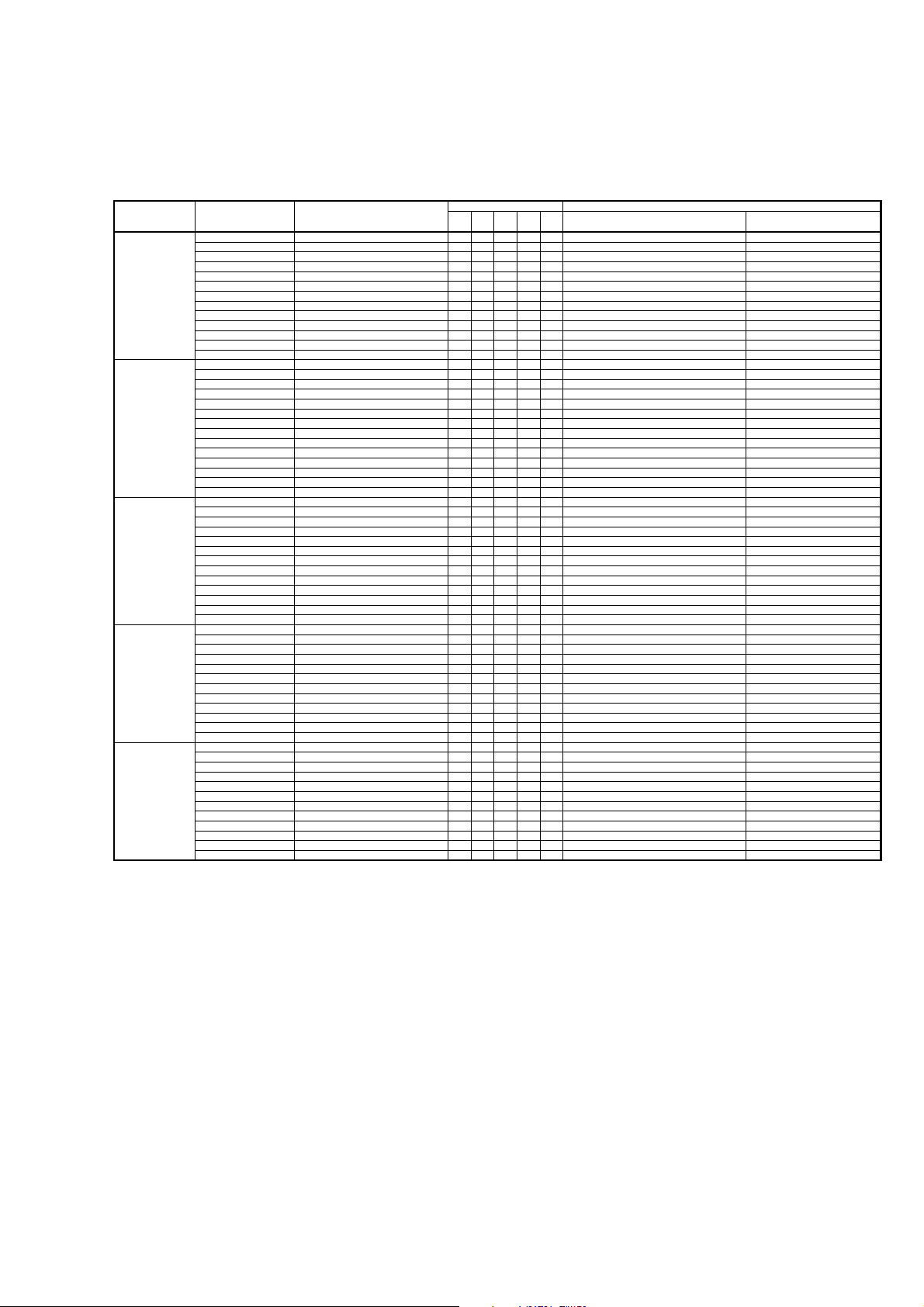
3. POWER AMPLIFIER ADJUSTMENT
Idling Current Alignment
1. Each of the measurement points are provided with the
two test points. Set a digital Voltage meter to DC voltage
input, connect the meter to the test points at both
contact points.
2. After the setup above, turn on the main switch.
3. Adjust variable resistors (VR41 - VR71) according to the
digital voltmeter readings. The target setting value is the
following table for each channel.
Settings: Master Volume — Minimum
Speaker out — No Load
Top lid — OPEN
Channel Alignment Point Measurement Point
Front L VR41 CN41
Center VR61 CN61
Front R VR51 CN51
Surround L VR42 CN42
Surround R VR52 CN52
Surround Back L VR62 CN62
Surround Back R VR71 CN71
アイドリング電流調整
1. 電源を ON する前にそれぞれの "+" 端子と "-" 端子間にデ
ジタルボルトメーターを接続します。デジタルボルトメー
ターを
DC 電圧入力にセットします。
2. 上記のセットアップの後に、本機の電源を ON します。
3. デジタルボルトメーターの電圧値を監視しながら可変抵抗
器
(VR41 〜 VR71) を調節します。
各チャンネルの目標値は下記の表を参照下さい。
セッティング
スピーカー接続 無し
トップカバー –– 無し
: マスター・ボリューム 最小
Time Table of Idling Current Rise
Ambient temperature
After T urning ON
10 min. 2.4 mV ± 0.3 mV
20 min. 2.4 mV ± 0.3 mV
30 min. 2.4 mV ± 0.3 mV
20 to 30 degrees centigrade
Measurement V oltage
9
Page 12
4. SERVICE MODE
4. SERVICE MODE
MAIN CPU Version, DSP Version, HDMI CPU Version and
Segment Check Mode
1. Connect the mains cord into the unit.
2. Press the POWER ON/STANDBY button for turn on the
unit.
3. Press the PURE DIRECT, 7.1CH INPUT and MultEQ
buttons simultaneously more then 3 seconds.
4. The FL display shows "SERVICE MODE" for 2 seconds
then shows the model name.
SERV I CE MODE
SR8001
5. Press the ENTER button, the software version of the
MAIN CPU (IC17) is displayed in the format below.
V060707 3N
Year
Month Date
Release No. Destination
MAIN CPU Version, DSP Version, HDMI CPU Version and
Segment Check Mode
1.
本機に電源コードを接続します。
2. POWER ON/STANDBYボタンを押し、本機の電源を入れ
ます。
3. PURE DIRECT, 7.1CH INPUT, MultEQの3つのボタンを
同時に
3秒以上押します。
4. FLに"SERVICE MODE"と2秒表示し、次にモデル名を表
示します。
SERVICE MODE
SR8001
5. ENTERボタンを押すと、MAINマイコン(IC17)のバージョ
ンが表示されます。
V060707 3N
Month DateYear
リリース No. 仕向け
6. Press the ENTER button again, the serial Number of the
unit is displayed.
MZ 294967295
7. Press the ENTER button, the software version of the TI
DSP (IC34) is displayed in the format below.
TI V038606121
Month DateYear
Release No.
8. Press the ENTER button, the software version of the
HDMI CPU (IC90) is displayed in the format below.
HDMI Ve r . h18
9. Press the ENTER button again, the left half, right half
and center of the label area in the FLD light on and off
each other.
10. Press the ENTER button again, the segments of the
character area in the FLD flick in checker pattern.
11. Press the ENTER button again, all the FL segments
turns off.
12. Press the ENTER button again to quit this mode.
6. 更にENTERボタンを押すと、シリアルナンバーが表示さ
れます。
MZ 294967295
7. 更にENTERボタンを押すと、TI DSP (IC34)のバージョン
が表示されます。
TI V038606121
Month DateYear
リリース No.
8. 更にENTERボタンを押すと、HDMI CPUのバージョンが
表示されます。
HDMI Ve r . h18
9. 更にENTERボタンを押すと、FLのラベル部分の左半分と
右半分および中心部が交互に点灯と消灯を繰り返します。
10. 更にENTERボタンを押すと、FLのキャラクタセグメント
部がチェッカーフラグのように点灯と消灯を繰り返しま
す。
11. 更にENTERボタンを押すと、FLは全消灯します。
12. 更にENTERボタンを押すと、サービスモードを終了しま
す。
10
Page 13

Product Reset
To reset the back up memory of the unit into the default
status, follow the procedure below.
Should the operation or display seem to be abnormal,
reset the unit with the following procedure.
To turn on the SR7001/SR8001, press and hold the
MULTI and SPEAKERS A/B buttons simultaneously for
3 seconds or more.
Remember that the procedure will reset the settings
of the function selector, Surround mode, delay time,
TUNER PRESET etc., to their initial settings.
Personal notes:
11
Page 14

5. SYSTEM ERROR
5. SYSTEM ERROR
1. Trouble in EEP-ROM (DSP PWB / IC15) Interface
CHECK E2P I F
• If the communication error that ACK did not return by
communication with EEP-ROM (DSP PWB / IC15)
occurred 2 seconds and more.
CHECKPOINT
1. Turn the power on. Are the IIC Clock Line (IC17/130pin
- IC15 / 6pin) normal?
2. Are the IIC Data Line (IC17/131pin - IC15 / 5pin)
normal?
3. Is +3.3V voltage supplied to 8pin of IC15?
4. When no problem to the above 1-3, replace IC15.
2. Trouble in +5V Supply
CHECK POW5
1. EEP-ROM (DSP PWB / IC15) Interface異常検出表示
• EEP-ROM (DSP PWB / IC15)との通信でACKが帰ってこ
ない状態(通信エラー)が約2秒以上生じた時に表示され
ます。
回路上の確認箇所
①
. Power ON時にIIC Clock Line (IC17/130pin - IC15 /
6pin)
が正常なのを確認する。
②
. Power ON時にIIC Data Line (IC17/131pin - IC15 /
5pin)
が正常なのを確認する。
③
. IC15 / 8pinにVCC (+3.3V)が供給されていることを確
認する。
④
. 上記の①−③に不具合が生じていない場合はIC15の不
良が考えられます。
2. +5V Supply異常検出表示
• If +5V inputted into 68pin of IC17 is troubled and the
following the fault of 1 - 4.
CHECKPOINT
1. Turn the power on. Is +5V voltage supplied to CN30/
6pin and CN30/7pin of DSP PWB.
2. Is the signal of IC17 H? 29pin (Power Amp Fail)= H.
(When 2 second or more "L" state is continuing to
29pin, Abnormalities have occurred in the POWER
AMP circuit.)
3. Is the signal of IC17 H? 66pin (Power Line Fail)= H.
(When the 2 second and more "L" state is continuing
to 66pin, Abnormalities have occurred to +-15V power
supply or the power supply for Power Amp.)
4. Is the signal of IC17 H? 77pin (Power Down)= H.
(When 2 second and more "L" state is continuing to
77pin, Abnormalities have occurred in IC74 and around
IC77 circuit of STANDBY PWB.)
3. Trouble in Protection
• 電源ON時に68pinに入力される+5Vの検出が出来なかった
場合に表示されます。
も同様の表示を行います。
又、下記の②〜④の不具合発生時に
回路上の確認箇所
①
. 電源ON時にCN30 (DSP PWB) 6,7pinに+5Vが供給さ
れていることを確認する。
②
. 電源ON時にマイコンの29pin (Power Amp Fail) が
"H"
になっていることを確認する。(29pinが電源ONし
てから2秒以上
AMP
回路に異常が発生している)
③
. 電源ON時にマイコンの66pin(Power Line F ail)が "H"に
なっていることを確認する。(
ら
2秒以上"L"状態が継続している場合は+/-15V電源又
は、
Power Amp用の電源に異常が発生している)
④
. 電源ON時にマイコンの77pin (Power Down)が "H"に
なっていることを確認する。(
も
"L"状態が継続している場合はSTANDBY PWB上の
"L"状態が継続している場合はPOWER
66pinが電源ONしてか
77pinが電源ONして
IC74及び周辺回路に異常が発生している)
3. PROTECTION検出表示
PROTECT
• When unusual states, such as overload of Power Amp
and DC output, are detected.
The unusual detection method is the following.
1. When "L" of 100 msec and more is detected by 29pin
(Power Amp Fail) of IC17, the unit will be in standby
mode and STANDBY LED will blink.
• Power Ampの過負荷、DC出力等の異常状態が検出された
際に表示されます。
また、異常検出は以下の様に行われます。
①
. マイコンの29pin (Power Amp Fail)に100msec以上
の
"L"検出がされた場合はSETをSTANDBY状態にし
て
Front Panel上のSTANDBY LEDを点滅状態にしま
す
12
Page 15
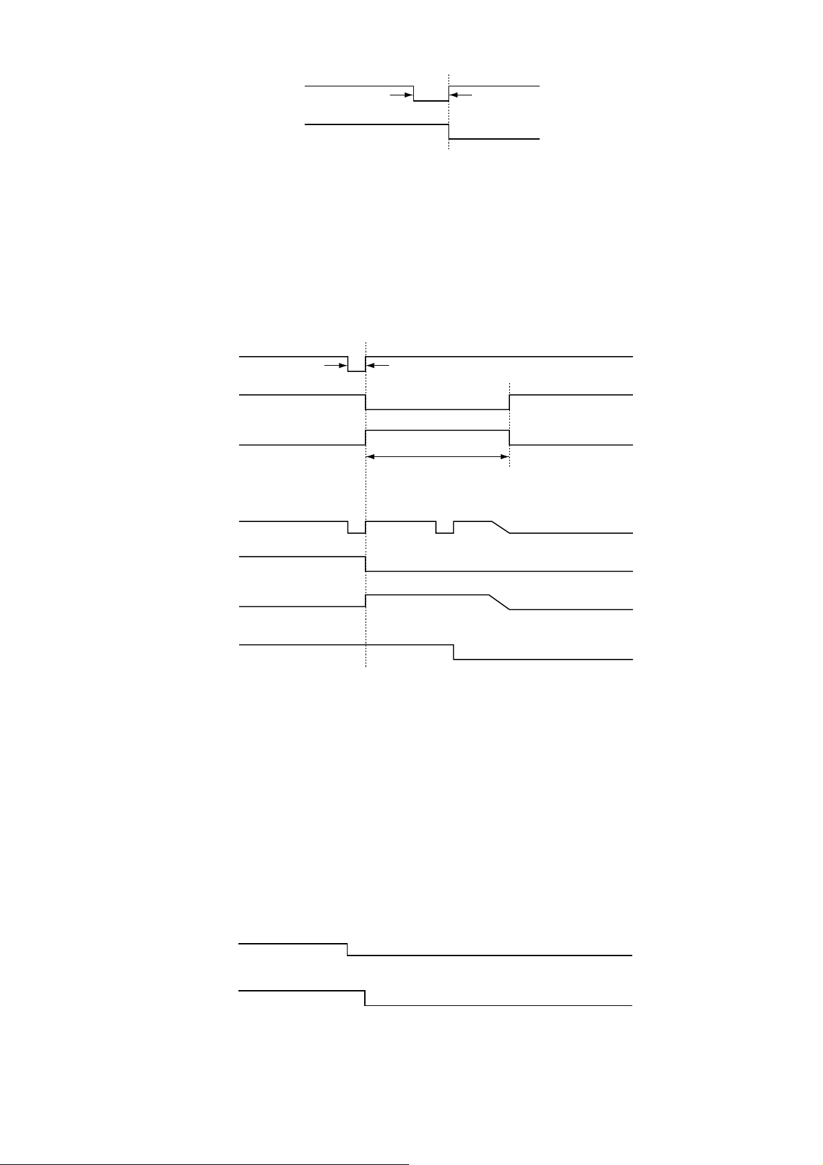
29pin(_P_AMP_FAIL)
43pin (_STANDBY)
100 msec and more
2. When "L" of less than 100msec is detected by 29pin
(Power Amp Fail) of IC17, Speaker Relay becomes
OFF and MUTE becomes ON state, and the state
is held for 8 seconds. At this time, "PROTECT" is
displayed. When similar abnormal detection was
considered to be it for these 8 seconds, the unit will
be in standby mode and STANDBY LED will blink.
When it was not detected abnormally for 8 seconds,
the unit returns to normal use state.
29pin(_P_AMP_FAIL)
Less than 100 msec
Speaker Relay
Mute
8Sec
"PROTECT" is displayed
29pin(_P_AMP_FAIL)
Speaker Relay
②. マイコンの29pin (Power Amp F ail)に100msec未満の
"L"
検出がされた場合はSpeaker RelayをOFF, MUTEを
ON状態にして8秒間その状態を保持する。この間、
FL Displayに "PROTECT"の表示を行う。この8秒間
に同様の異常検出がされた場合は
態にして
Front Panel上のSTANDBY LEDを点滅状態
にします。8秒間、異常検出されなかった時は
SETをSTANDBY状
SETを
通常使用状態に戻します。
Mute
43pin (_STANDBY)
CHECKPOINT
1. Check AMP PWB.
2. When AMP does not have a problem, it is confirmed
whether there is not abnormality by disconnection
of pattern of 29pin (Power Amp Fail) and the detect
circuit.
4. Trouble in Other
(The contents of detection are not indicated to FL.)
• When the abnormalities of ±15V power supply and the
±power supply for Power Amp are detected, the unit
will be in standby mode. The detection is performed by
66pin (P LINE FAIL).
66pin (_P_LINE_FAIL)
43pin (_STANDBY)
回路上の確認箇所
①
. Power Ampに不具合が生じている場合は修理を行
う。
②
. Power Ampに不具合が無い場合は、29pin (P ower Amp
Fail)
のパターンの断線及び検出回路に異常が無いか確
認する。
. その他の異常検出
4
(FLにCaution表示はしません)
• ±15V電源及び、Power Amp用の±電源の異常を検出
した場合、
(_P_LINE_FAIL)
SETをSTANDBYにします。 検出は66pin
で行われます。
CHECKPOINT
1. Check Power supply circuit.
2. When Power supply circuit does not have a problem,
it is confirmed whether there is not abnormality by
disconnection of pattern of 66pin (Power Line Fail)
and the detect circuit.
回路上の確認箇所
①
. 上記の電源回路に不具合が生じている場合は修理を行
う。
②
. 電源回路に不具合が無い場合は、66pin (Power Line
Faill)
13
確認する。
のパターンの断線及び検出回路に異常が無いか
Page 16
6. UPDATE FIRMWARE
[A] SOFTWARE (fdtv306r00.exe) DOWNLOADS
AND INSTALLS PROCEDURE
[A-1] DOWNLOADS OF THE SOFTWARE
(Flash Development Toolkit: the rest is FDT)
Download the software for update of the HDMI CPU.
1. Launch the browser.
2. Type the "http://www.renesas.com/" into an address. And
click the Go or press the Enter on keyboard of PC.
NOTE : This site is managed by RENESAS. The following
explanation may differ from the actual composition.
When different, please proceed along with the site
composition of RENESAS.
3. Click the GLOBAL SITE.
6. UPDATE FIRMWARE
[A] SOFTWARE (fdtv306r00.exe) DOWNLOADS AND
INSTALLS PROCEDURE
[A-1] DOWNLOADS OF THE SOFTWARE
(Flash Development Toolkit:
HDMI
マイコンの書き込みのためのソフトウェア(FDT)をダウ
ンロードします。
1. ブラウザ(インターネットエクスプローラーなど)を立ち上
げます。
2.
ブラウザのアドレスに"http://www.renesas.com/"を入力
し、
注意:このサイトは
3. GLOBAL SITEをクリックします。
移動、またはキーボードのEnterを押します。
RENESASが管理しているため、以下の説
明が実際のサイト構成と異なっている場合があります。
その場合は実際の
てください。
RENESASのサイト構成に沿って進め
以下 FDT)
14
Page 17
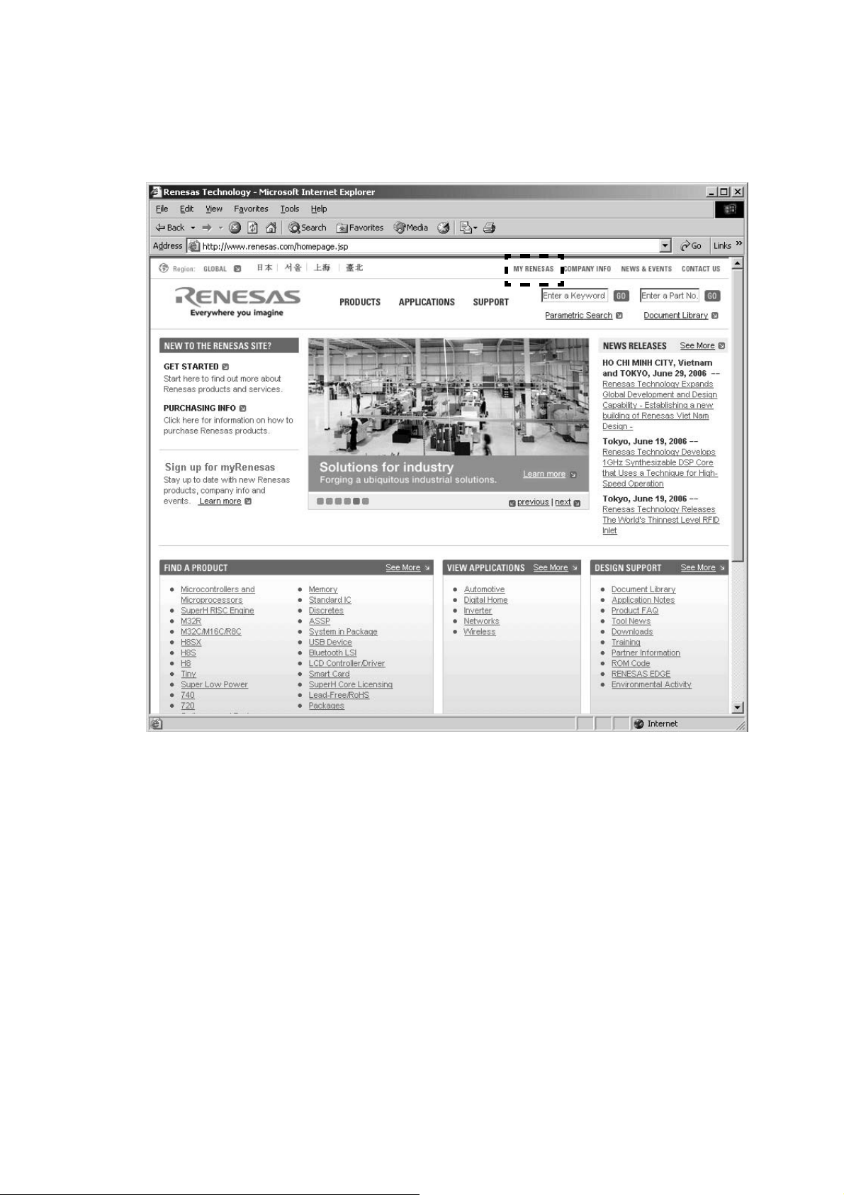
4. A login ID is necessary to download the FDT.
If you have Login ID, please advance to step 15.
If you do not have Login ID, Click the MY RENESAS.
4. FDTのダウンロードにはLogin IDが必要になります。
既にLogin IDを持っている方は手順の15へ進んでくださ
い。
Login IDを持っていない方はMY RENESASをクリックし
ます。
15
Page 18
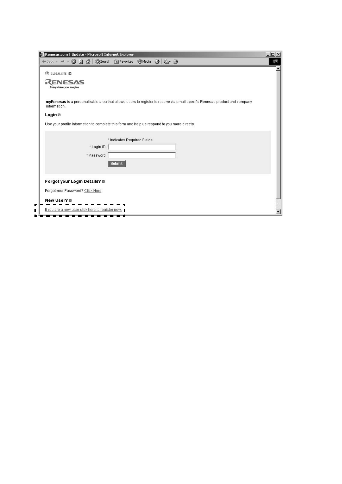
5. Click the If you are a new user click here to register
now.
5. If you are a new user click here to register nowをク
リックします。
16
Page 19
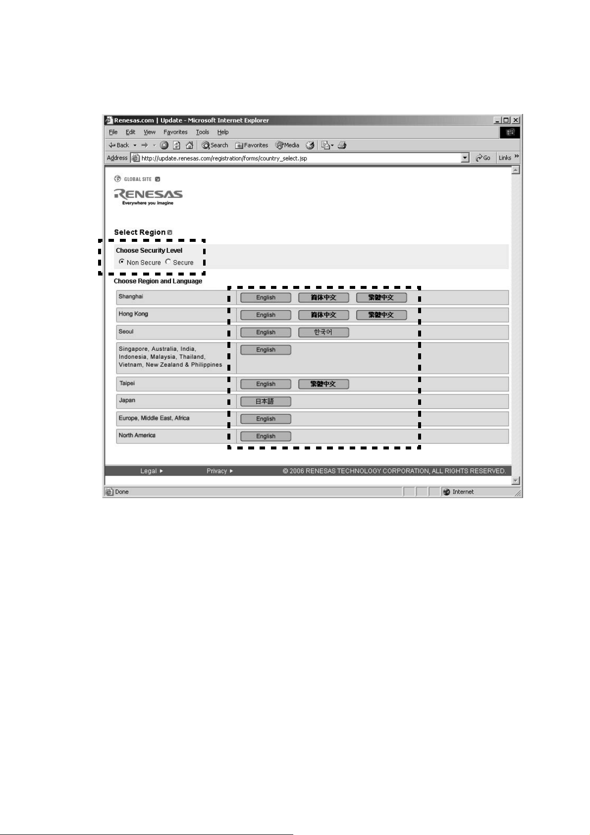
6. Choose Non Secure or Secure in Security Level at your
network environment.
Choose English or another one in Region and
Language.
6. PCのネットワーク環境によりChoose Security Levelか
ら
Non Secure、またはSecureを選んでください。
Choose Region and Languageから日本語をクリックしま
す。
17
Page 20
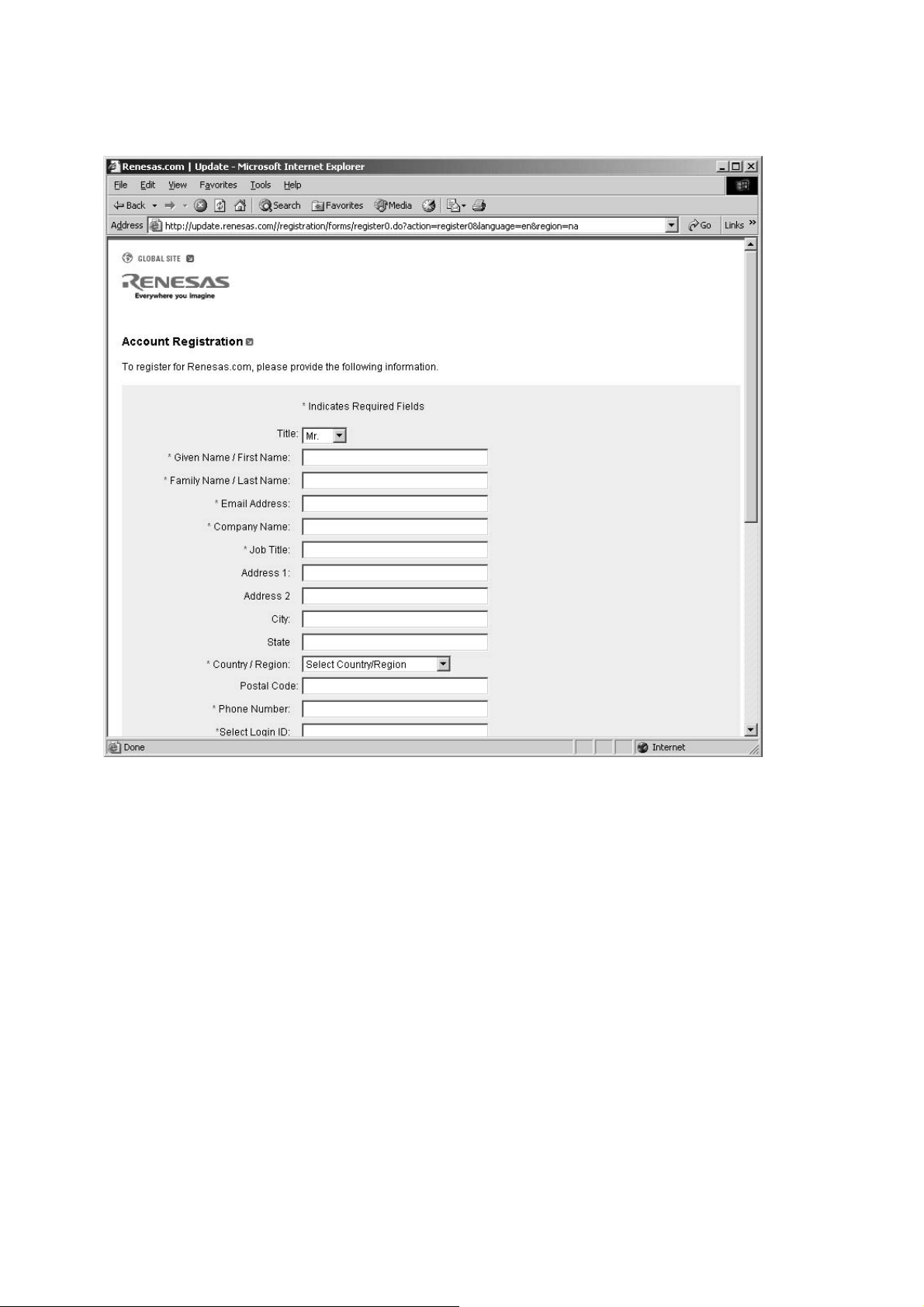
7. Input the each item.
NOTE : The items displayed by a language and region are
different.
7. 各項目を記入します。
注意:下記説明は英語ですが、日本語を選んだ場合日本語で表
示されます。
18
Page 21
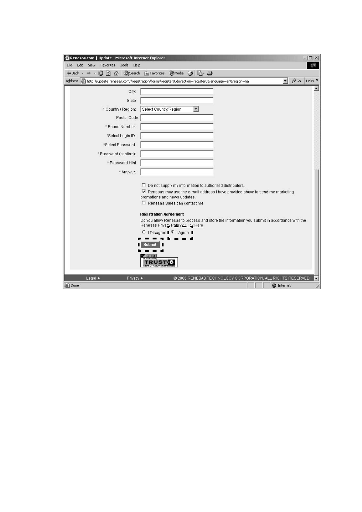
8. If you have inputted the necessary items, check the I
Agree, and click the Submit.
8. 必須項目を入力したならば、同意しますにチェックを入
れ、送信をクリックします。
19
Page 22
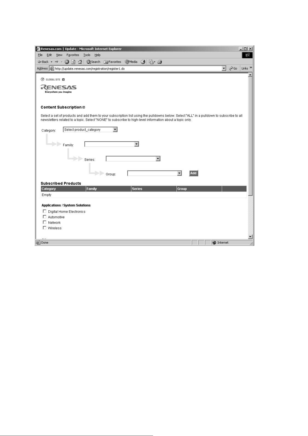
9. The input is needless in this page.
Scroll down the page.
9. このページは入力しなくても結構です。
ページをスクロールダウンします。
20
Page 23
10. Click the Submit.
10. 送信をクリックします。
21
Page 24
11. Immediately, an E-mail arrives from the RENESAS.
Click the link in the E-mail to go to the registration site,
and input the Login ID and Password.
And Click the Submit.
11. 直ちに、RENESASからE-mailが届きます。
E-mail内に有る登録サイトへのリンクをクリックします。
Login IDとPasswordを入力しSubmitをクリックします。
12. Registration is finished.
13. Open the RENESAS top page from registration page.
12.
登録が完了します。
13. 登録ページに有るリンクからRENESASのトップページに
移動します。
22
Page 25
14. Click the GLOBAL SITE.
14. GLOBAL SITEをクリックします。
23
Page 26
15. Click the Downloads in the DESIGN SUPPORT.
15. DESIGN SUPPORT内のDownloadsをクリックします。
24
Page 27
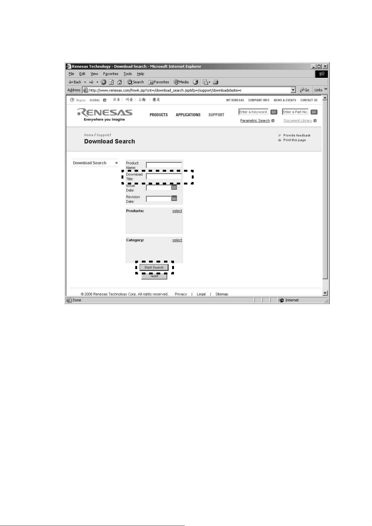
16. Type the "Flash Development toolkit" into the Download
Title.
And click the Start Search.
16. Download Titleに"Flash Development toolkit"を入力しま
す。
Start Searchをクリックします。
25
Page 28
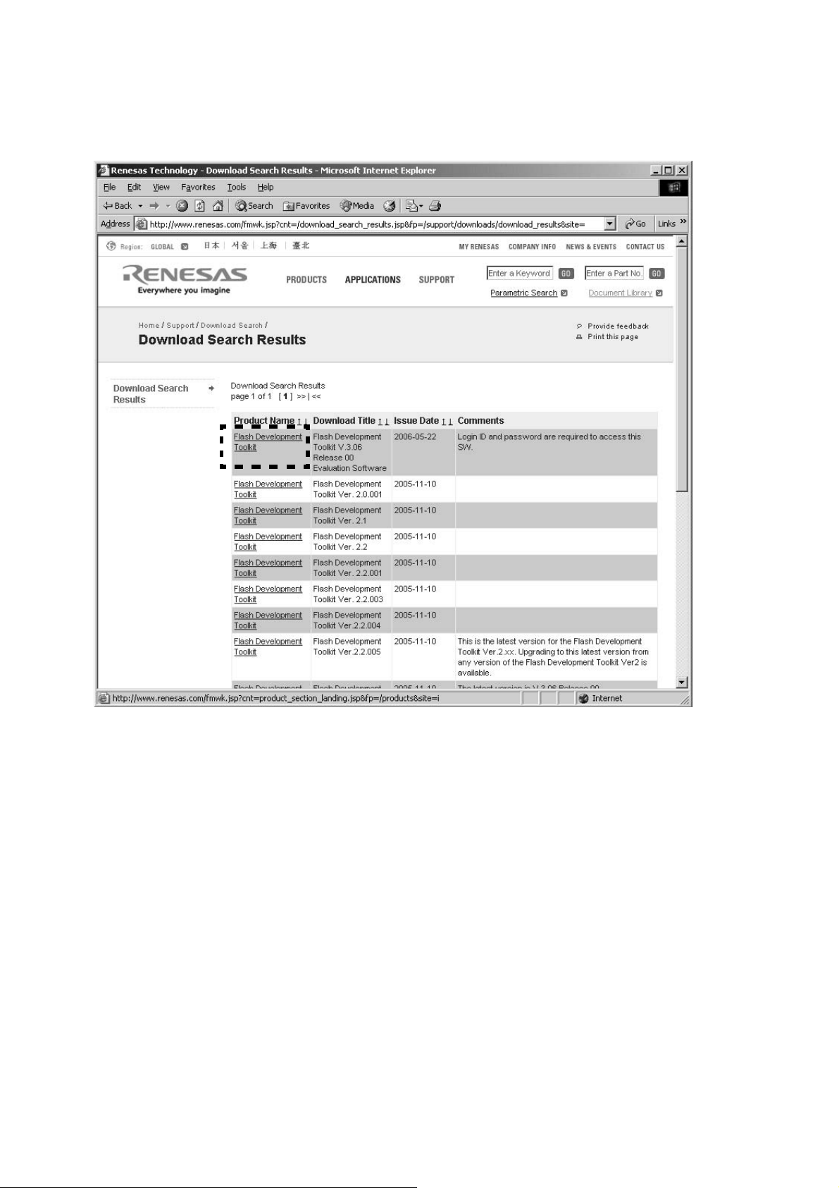
17. Click the Flash Development Toolkit of the top on the
table.
NOTE : The latest edition is FDT V3.06 at present. (July,
2006) It is in FDT V3.06 as follows and explains it.
17. 検索結果の一番上のFlash Development Toolkitをクリッ
クします。
注意:現時点
(2006年7月)での最新バージョンはV3.06になり
ます。以下
FDT V3.06で説明します。
26
Page 29
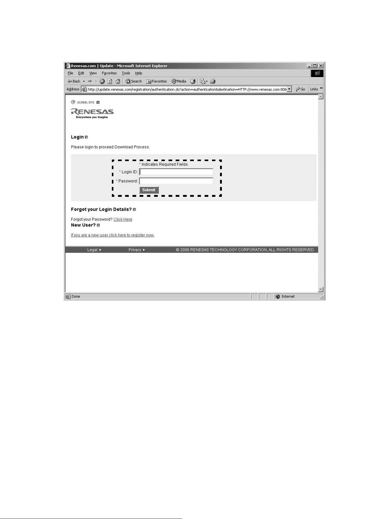
18. Input the Login ID and Password.
And click the Submit.
18. ダウンロードするためにLogin IDとPasswordを入力しま
す。
Submit.をクリックします。
27
Page 30
19. Scroll down the page.
19. ページをスクロールダウンします。
28
Page 31

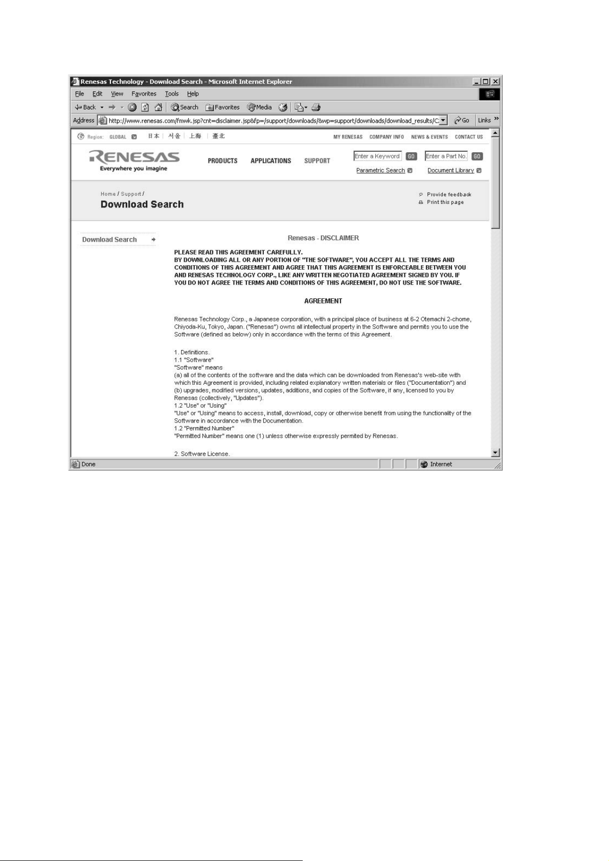
20. Check the Agree, and click the Submit.
20. Agreeにチェックを入れ、Submitをクリックします。
29
Page 32

21. Scroll down the page.
21. ページをスクロールダウンします。
30
Page 33

22. Click the Download.
22. Downloadをクリックします。
31
Page 34

23. Click the Save.
23. Saveをクリックします。
24. Save the fdtv306r00.exe on your PC’s hard disc.
NOTE : A file name is change by improvement.
24. fdtv306r00.exe
注意:ファイル名はバージョンにより変わります。
を任意のフォルダに保存します。
32
Page 35

[A-2] INSTALLS OF THE SOFTWARE
(Flash Development Toolkit Ver.3.06)
1. Open the folder with the downloaded file.
2. And double click the fdtv306r00.exe.
[A-2] INSTALLS OF THE SOFTWARE
(Flash Development Toolkit Ver.3.06)
1.
ダウンロードしたファイルのあるフォルダを開きます。
2. fdtv306r00.exeをダブルクリックします。
3. Click the Next.
3. Next
をクリックします。
33
Page 36

4. Check the International [English], and click the Next.
4. International [English]にチェックを入れNextをクリッ
クします。
5. Check the I accept the terms of the license
agreement, and Click the Next.
5. I accept the terms of the license agreement
クを入れ、
Nextをクリックします。
にチェッ
34
Page 37

6 Click the Next.
6. Nextをクリックします。
7. Check the all file type, and Click the Next.
7.
全てのファイルタイプにチェックを入れ、Nextをクリック
します。
35
Page 38

8. Click the Next.
8. Nextをクリックします。
9. Click the Install.
9. Install
をクリックします。
36
Page 39

10. The Setup Status bar appears.
10. インストールの状態が表示されます。
11. Click the Finish.
11. Finish
をクリックします。
37
Page 40

12. Click the OK.
12. OKをクリックします。
38
Page 41

[B] WRITING AND UPDATE SOFTWARE
Software for MAIN CPU, flash ROM for DSP and HDMI
CPU can be updated/downloaded.
Have update/download application software. ("H8Download.
exe", "da708_writer.exe" and "fdtv306r00.exe (FDT3.06) or
latest version")
[B] WRITING AND UPDATE SOFTWARE
MAINマイコン、DSPのフラッシュROM、およびHDMIマイコ
ンのソフトウェアは更新、および書き込みが出来ます。
更新および書き込みには書き込み用アプリケーション
が必要です。
exe
、"fdtv306r00.exe (FDT3.06)または最新版")
("H8Download.exe"、da708_writer.
There are three mode of download, regarding to the target of
software as bellow.
Mode 1: Update/Download MAIN CPU's software to
internal Flash-ROM.
This mode is to update/download the software for MAIN
CPU.
The target devise is internal flash ROM of CPU (IC17) on
CUP11872Z (DSP PWB).
The unit needs to be set to writing condition, by pushing
internal switch from rear panel.
The updating of software takes about 2 minutes and 30
seconds.
Mode 2: Update/Download DSP's software to 8M Flash-
ROM.
This mode is to update/download the software for DSP.
The target devise is 8M Flash-ROM (IC34) on
CUP11872Z (DSP PWB).
The unit needs to be set writing condition, by three front
buttons.
The updating of software takes about 2 minutes.
Mode 3: Update/Download HDMI CPU's software to
internal Flash-ROM.
This mode is to update/download the software for HDMI
CPU.
The target devise is internal flash ROM of CPU (IC90) on
CUP11875Z (HDMI PWB).
The unit needs to be set writing condition, by three front
buttons.
The updating of software takes about 45 seconds.
NECESSARY EQUIPMENT
The following items are required for updating/downloading.
Windows PC (OS: Windows2000 or WindowsXP) with
Serial port.
RS-232C Dsub-9 pin cable (female to female/straight
type)
Update software to MAIN CPU. (H8Download.exe, etc...
in MAIN folder)
Update software to flash ROM for DSP. (da708_writer.
exe, etc... in DSP folder)
Update software to HDMI CPU. (Writing data in HDMI
folder)
Flash Development Toolkit 3.06 or latest version
(fdtv306r00.exe or latest version)
Use RS232C Dsub-9 pin cable (female to female/straight
type) to connect PC and the RS-232C port in rear panel of
the unit, when updating/downloading MAIN CPU DSP and
HDMI CPU.
書き込みには下記の3つのモードがあります。
Mode 1: Update/Download MAIN CPU's software to
internal Flash-ROM.
このモードはMAINマイコンの更新および書き込み用です。
基板CUP11872Z (DSP PWB)のIC17のマイコン内部のフラ
ッシュ
ROMに書き込みます。
本機のリアパネルから内部スイッチを押し、書き込みモー
ドにする必要があります。
書き込みにかかる時間は約2分30秒です。
Mode 2: Update/Download DSP's software to 8M Flash-
ROM.
このモードはDSPのフラッシュROMの更新および書き込み
用です。
基板CUP11872Z (DSP PWB)のIC34のフラッシュROMに
書き込みます。
本機のフロントボタン3つから書き込みモードにする必要が
あります。
書き込みにかかる時間は約2分です。
Mode 3: Update/Download HDMI CPU's software to
internal Flash-ROM.
このモードはHDMIマイコンの更新および書き込み用です。
基板CUP11875Z (HDMI PWB)のIC90のマイコン内部のフ
ラッシュ
ROMに書き込みます。
本機のフロントボタン3つから書き込みモードにする必要が
あります。
書き込みにかかる時間は約45秒です。
必要機器
下記は更新および書き込みに必要な機器です。
Windows PC (OS : Windows2000 またはWindowsXP) で
Serial ポートのあるもの
RS-232C ストレートケーブル(9Pin メス-9Pin メス)
MAIN
マイコン用書き込みソフトウェア(MAINフォルダ内
H8Download.exe、など)
DSP
HDMI
Flash Development Toolkit 3.06
MAIN
トウェアを更新および書き込みする場合、
本機リアパネルの
ートを接続します。
フラッシュROM用書き込みソフトウェア(DSPフォル
ダ内
da708_writer.exe、など)
マイコン用書き込みソフトウェア(HDMIフォルダ内書
き込み用データ
exe
または最新版)
マイコン、DSPフラッシュROM、HDMIマイコンのソフ
)
または最新版 (fdtv306r00.
RS-232Cケーブルで
RS232CコネクタとWindows PCのSerialポ
39
Page 42

Mode 1: Update/Download MAIN CPU's software to
internal Flash-ROM
Update/Download software for MAIN CPU (Mode 1)
1. Put the "MAIN" folder into anywhere on your PC's hard
disc.
Mode 1: Update/Download MAIN CPU's software
to internal Flash-ROM
Update/Download software for MAIN CPU (Mode 1)
1. "MAIN"
フォルダをPCの任意のフォルダにコピーします。
2. Connect RS-232C on the rear panel of the unit and
Serial Port of windows PC with RS-232C cable.
3. Insert a thin rot to the hole near the MULTI RC OUT
terminal and push the switch (SW10) inside to turn on
the switch.
4. Connect the mains cord into the unit. And press the
POWER ON/STANDBY button for turn on the unit.
(Except U1B)
NOTE : When the unit is into boot mode, STANDBY LED is
lights at green.
本機のリアパネルにあるRS-232CコネクタとWindows
2.
PC
のSerialポートをRS-232Cケーブルで接続します。
3. 細い棒を使い本機のMULTI RC OUT端子の右となりにあ
る穴から内部スイッチ
します。
4. 本機に電源ケーブルを差し、POWER ON/STANDBYボタ
ンを押して電源を入れます。
注意:本機が書き込みモードになると
点灯します。
(SW10)を押して書き込みモードに
Push switch (SW10)
Hole of rear panel
STANDBY LEDが緑色に
40
Page 43

5. Double click the H8Download.exe. And launch the
marantz firmware upgrade program.
5. H8Download.exeをダブルクリックし、marantz firmware
upgrade program
を起動します。
6. Click the Set Ports.
7. Choose the COM Port number. And Click the OK.
6. Set Ports
をクリックします。
使用するCOMポート番号を選択し、OKをクリックしま
7.
す。
41
Page 44

8. Click the other files... in the Firmware program file.
9. Choose the SR8001_yymmddv.mot. And click the Open.
NOTE : The yy is two digits of year. The mm is month. The
dd is date. The v is release number.
8. Firmware program file内のother files...をクリックしま
す。
9. SR8001_yymmddv.mot
す。
注意:
yyは年の下二桁、mmは月、ddは日、vはリリースナン
バー
を選択し、Openをクリックしま
42
Page 45

10. Click the Connect.
10. Connectをクリックします。
11. If the connection with the H8 µ-P is successfully made, a
dialogue box saying "Success to the H8 micro processor
connection" appears. If the connection fails, error
message will appear.
Click the OK.
12. Click the Send to start update/download.
The writing of software takes about 2 minute and 30
seconds.
マイコンとの接続に成功すると"Success to the H8
11. H8
micro processor connection"
スが表示されます。接続に失敗するとエラーメッセージが
表示されます。
と表示したダイアログボック
OKをクリックします。
12. Send
書き込みにかかる時間は約
をクリックし書き込みを開始します。
2分30秒です。
43
Page 46

13. If the firmware is updated/downloaded successfully,
a dialog box saying "Finished the firmware program
sending" appears.
Click the OK.
13. 書き込みが成功すると"Finished the firmware program
sending"
と表示したダイアログボックスが表示されます。
OKをクリックします。
14. Click the Close to close the application.
15. Press the POWER ON/STANDBY button for turn off the
unit. (Except U1B)
16. Disconnect the mains cord and RS-232C cable from the
unit.
17. Insert a thin rot to the hole and push the switch (SW10)
inside to turn off the switch.
14. Close
をクリックしアプリケーションを閉じます。
15. POWER ON/STANDBY
ます。
ボタンを押して本機の電源を切り
16. 電源ケーブルとRS-232Cケーブルを本機から外します。
17. 細い棒を使い本機のMULTI RC OUT端子の右となりにあ
る穴から内部スイッチ
解除します。
(SW10)を押して書き込みモードを
44
Page 47

Mode 2 : Update/Download DSP’s software to 8M
Flash-ROM
Update/Download Software for DSP (Mode 2)
1. Put the "DSP" folder into anywhere on your PC's hard
disc.
Mode 2: Update/Download DSPs software to 8M
Flash-ROM
Update/Download Software for DSP (Mode 2)
1. "DSP"
フォルダをPCの任意のフォルダにコピーします。
2. Connect the RS-232C on rear panel of the unit and the
Serial Port of windows PC with RS-232C cable.
3. Connect the mains cord into the unit.
4. Press the POWER ON/STANDBY button for turn on the
unit.
5. Press the ENTER, SURROUND MODE and T -MODE
buttons simultaneously more than 3 seconds to turn the
unit into Loading Mode.
6. The FLD shows "SELECT DSP" after showed
"LOADING MODE".
7. Press the ENTER button.
8. "SELECTED DSP" shows on the FLD.
本機のリアパネルにあるRS-232CコネクタとWindows
2.
PC
のSerialポートをRS-232Cケーブルで接続します。
3. 本機に電源ケーブルを差します。
4. POWER ON/STANDBYボタンを押し、本機の電源を入れ
ます。
5. ENTER, SURROUND MODE, T -MODEの3つボタンを同
時に
3秒以上押し続け、本機をローディングモードにしま
す。
6. FLに"LOADING MODE"と表示された後、"SELECT
DSP"
と表示されます。
7. ENTERボタンを押します。
8. FLの表示が"SELECTED DSP"に変わります。
45
Page 48

9. Double click the da708_writer.exe. And Launch the
SR8001 TI Writer.
9. da708_writer.exeをダブルクリックし、SR8001 TI
Writer
を起動します。
10. Choose the COM Port number.
11. Click the Connect.
使用するCOMポート番号を選択します。
10.
11. Connect
をクリックします。
46
Page 49

12. "Connection OK!!" appears on SR8001 TI Writer. And
click the FileOpen.
12. SR8001 TI Writer上に"Connection OK!!"と表示された
ら、
FileOpenをクリックします。
13. Choose the pa17_meqyymmdd_vv.upd. And click the
Open.
NOTE : The yy is two digits of year. The mm is month. The
dd is date. The vv is release number.
13. pa17_meqyymmdd_vv.upd
ます。
注意:
yyは年の下二桁、mmは月、ddは日、vvはリリース番号
を選択し、Openをクリックし
14. Click the OK.
47
14. OK
をクリックします。
Page 50

15. Click the SEND.
16. Software is written into the DSP Flash ROM.
The writing of software takes about 2 minute.
15. SENDをクリックします。
16.
ソフトウェアがDSPフラッシュROMに書き込まれます。
書き込みにかかる時間は約2分です。
17. Click the OK.
19. Click the Discon.
17. OK
をクリックします。
18. Discon
をクリックします。
48
Page 51

19. Click the Exit.
19. Exitをクリックします。
20. Press the POWER ON/STANDBY button for turn off the
unit.
21. Disconnect the mains cord and RS-232C cable from the
unit.
20. POWER ON/STANDBY
ます。
ボタンを押し、本機の電源を切り
21. 本機から電源コードとRS-232Cケーブルを外します。
49
Page 52

Mode 3: Update/Download HDMI CPU's software to
internal Flash-ROM.
Update/Download software for HDMI CPU (Mode 3)
[M3-1] The writing software setup procedure
1. Launch the Flash Development Toolkit v3.06 (FDT).
NOTE : Please refer to "[A] SOFTWARE (fdtv306r00.exe)
DOWNLOAD AND INSTALL PROCEDURE", when
you do not have FDT.
Can NOT update/download software by
FDT ver.3.3.
2. Click Start, Programs, Renesas, Flash Development
Toolkit 3.06 and Flash Development Toolkit 3.06.
Mode 3: Update/Download HDMI CPU's software
to internal Flash-ROM.
Update/Download software for HDMI CPU (Mode 3)
[M3-1] The writing software setup procedure
1. Flash Development Toolkit v3.06 (FDT)
注意:
FDTを持っていない方は"[A] SOFTWARE (fdtv306r00.
exe) DOWNLOAD AND INSTALL PROCEDURE"
照してダウンロードしてください。
この書き込みはFDT ver.3.3では出来ません。
2. Start, Programs, Renesas, Flash Development
Toolkit 3.06, Flash Development Toolkit 3.06
クします。
を起動します。
を参
をクリッ
3. Check the Create a new project workspace, and click
the OK.
NOTE : It is needs setup for SR7001/SR8001. When you
have already setup, please advance to "[M3-2]
Writing Procedure for HDMI CPU".
3. Create a new project workspace
クリックします。
注意:
SR7001/SR8001用の設定が必要です。既に設定が終
わっている方は
CPU"
へ進んでください。
"[M3-2] Writing Procedure for HDMI
をチェックし、OKを
50
Page 53

4. SR8001_HDMI is inputted into the Workspace Name.
(It is simultaneously inputted into Project Name.)
Click the OK.
4. Workspace NameにSR8001_HDMIを入力します。
(同時にProject Nameにも入力されます)
OK
をクリックします。
5. Choose the H8/36087F in Select Device. And click the
Next.
5. Select Device
します。
からH8/36087Fを選択し、Nextをクリック
51
Page 54

6. Choose the Serial port number in the Select Port. And
click the Next.
6. Select PortからSerialポート番号を選び、Nextをクリック
します。
7. 16.0000 is inputted into the Enter the CPU crystal
frequency for the selected device. And click the Next.
7. Enter the CPU crystal frequency for the selected device
に16.0000を入力し、Nextをクリックします。
52
Page 55

8. Check The BOOT Mode in Select Connection.
Un-check the Use Default, and choose the 19200 in
Recommended Speeds.
Click the Next.
8. Select ConnectionのBOOT Modeをチェックします。
Recommended SpeedsのUse Defaultのチェックを外
し、
19200を選択します。
Nextをクリックします。
9. Check the Automatic in Protection.
Check the Advanced in Messaging.
Click the Finish.
9. Protection
のAutomaticをチェックします。
MessagingのAdvancedをチェックします。
Finishをクリックします。
53
Page 56

[M3-2] Writing Procedure for HDMI CPU
1. Connect the RS-232C on rear panel of the unit and the
Serial Port of windows PC with RS-232C cable.
2. Connect the mains cord into the unit.
3. Launch the Flash Development Toolkit (FDT), When
FDT is not launch.
When FDT is already launch, please advance to step
No.7.
4. Click Start, Programs, Renesas, Flash Development
Toolkit 3.06 and Flash Development Toolkit 3.06.
[M3-2] Writing Procedure for HDMI CPU
1.
本機のリアパネルにあるRS-232CコネクタとWindows
PC
のSerialポートをRS-232Cケーブルで接続します。
2. 本機に電源コードを接続します。
3. Flash Development Toolkit v3.06(FDT)を起動していない
場合は起動します。
既にFDTを起動している方はステップ7に進んでくださ
い。
4. Start, Programs, Renesas, Flash Development
Toolkit 3.06, Flash Development Toolkit 3.06
クします。
をクリッ
5. Check the Browse to another project workspace, and
click OK.
5. Browse to another project workspace
OKをクリックします。
をチェックし、
54
Page 57

6. Choose SP8001_HDMI.AWS in SR8001_HDMI folder
under workspase folder. And Click the Open.
6. workspaseフォルダの下のSR8001_HDMIフォルダ内の
SP8001_HDMI.AWS
す。
を選択し、Openをクリックしま
7. Right button of mouse click on the SR8001_HDMI, and
select the Add Files... in a menu.
7. SR8001_HDMI
Files...
をクリックします。
を右クリックし、メニューからAdd
55
Page 58

8. Choose the HDMI_REPV2xyymmddvv.mot, and click
the Add.
NOTE : The yy is two digits of year. The mm is month. The
dd is date. The vv is release number.
8. HDMI_REPV2xyymmddvv.motを選択し、Addをクリッ
クします。
注意:
yyは年の下二桁、mmは月、ddは日、vvはリリースナ
ンバー
9. Press the POWER ON/STANDBY button for turn on the
unit.
10. Press the ENTER, SURROUND MODE and T-MODE
buttons simultaneously more than 3 seconds to turn the
unit into Loading Mode.
11. The FLD shows "SELECT DSP" after showed
"LOADING MODE".
12. Turn the INPUT SELECTOR to change display from
"SELECT DSP" to "SELECT HDMI" on FLD.
13. Press the ENTER button.
14. "SELECTED HDMI" shows on the FLD.
9. POWER ON/STANDBY
ます。
ボタンを押し、本機の電源を入れ
10. ENTER, SURROUND MODE, T-MODEの3つボタンを同
時に
3秒以上押し続け、本機をローディングモードにしま
す。
11. FLに"LOADING MODE"と表示された後、"SELECT
DSP"
と表示されます。
12. 本機のINPUT SELECTORを回して、FLの表示
が
"SELECT DSP"から"SELECT HDMI"に換えます。
13. ENTERボタンを押します。
14. FLの表示が"SELECTED HDMI"に変わります。
56
Page 59

15. Click the Device in the menu bar and select the
Connect to Device.
15. Deviceをクリックし、メニューからConnect to
Device
をクリックします。
16. Press right button of mouse on the HDMI_
REPV2xyymmddvv.mot, and select the Download File
in a menu.
16. HDMI_REPV2xyymmddvv.mot
ーから
Download Fileをクリックします。
を右クリックし、メニュ
57
Page 60

17. Software is written into the HDMI CPU.
The writing of software takes about 45 seconds.
17. ソフトウェアがHDMIマイコンに書き込まれます。
書き込みにかかる時間は約45秒です。
18. Click the Device in the menu bar and select the
Disconnect.
18. Device
クします。
をクリックし、メニューからDisconnectをクリッ
58
Page 61

19. Click the File and select the Exit in menu.
19. Fileをクリックし、メニューからExitをクリックします。
20. Press the POWER ON/STANDBY button for turn off the
unit.
21. Disconnect the mains cord and RS-232C cable from the
unit.
20. POWER ON/STANDBY
ます。
ボタンを押し、本機の電源を切り
21. 本機から電源コードとRS-232Cケーブルを外します。
59
Page 62

Personal notes:
60
Page 63

7. WIRING DIAGRAM
-!).42!.3&
34!.$"907"
#50:
3",230%!+%207"
#50:
0/7%207"
#50:
#.0
!-007"
#50:
*7*70X
*7*7*7*7
*70X
2%'5,!4/207"
#50:
#/-0/.%.407"
32#50:
32#50:
6)$%/07"
#50:
$3007"
#50:
23#07"
#50:
($-)07"#50:
8-07"
#509
45.%2-/$5,%
3%,%#4/2
%.#/$%207"
#50:
053(3707"
#50:
4!#407"
(007"
#50:
&2/.407"
#50:
6/,5-%07"
#50:
#().05407"
#50:
'5)$%07"
#50:
).05407"#50:
#(02%/5407"
#50:
61 62
Page 64

8. BLOCK DIAGRAM
U02/$300!24
($&
U02/
4-3$!
$3$
6463
Page 65

U02/
($&(6
65 66
Page 66

9. SCHEMATIC DIAGRAM
VIDEO PWB
&2/-2%'5,!4/207"
/3$
&2/-($-)07"
&2/-#/-0/.%.407"
&2/-&2/.407"
&2/-$3007"
&2/-
#/-0/.%.4
07"
&2/-($-)07"
&2/-($-)07"
6867
Page 67

COMPONENT PWB
&2/-
($-)07"
&2/-
6)$%/07"
&2/-
6)$%/07"
69 70
Page 68

HDMI PWB -1/4
#ABLE%QUALIZER
WITHSYSTEM
3WITCHING&UNCTION
4/($-)07"4/($-)07"
#ABLE%QUALIZER
WITHSYSTEM
3WITCHING&UNCTION
7271
Page 69

HDMI PWB -2/4
&2/-($-)07"
($-)/54
($-)42!.3-)44%23
&2/-($-)07"
($-)2%#%)6%23
($-)/54
($-)42!.3-)44%23
73 74
Page 70

HDMI PWB -3/4
BIT-(Z6IDEO%NCODERWITH.36AND
-ACROVISION®#OPY0ROTECTION
3$46($466IDEO$ECODER
AND
2'"'RAPHICS$IGITIZER
)0#/.6%24%2
4/($-)07"
4/6)$%/07"4/6)$%/07"
4/#/-0/.%.407"
7675
Page 71

HDMI PWB -4/4
.#
-ICROPROCESSOR
&2/-6)$%/07"
77 78
Page 72

INPUT PWB
&2/-$3007"
&2/-&2/.407"
4/$3007"
&2/-#.
4/!-007"
4/!-007"
3934%-%,%#42/.)#6/,5-%#/.42/,
&2/--!0!24
&2/--"0!24
!.!,/'37)4#(!22!9
!.!,/'37)4#(!22!9
&2/-#(02%/5407"
4/-5,4)!/54
4/-5,4)"/54
&2/-#().05407"
&2/-$3007"
4/$3007"
4/"#
&2/-2%'5,!4/207"
&2/-$3007"
8079
Page 73

DSP PWB 1/2
&2/-&2/.407"
4/8-07"
4/23#07"
4/2%'5,!4/207"
4/8-07"
4/0/7%207"
-ICROPROCESSOR
4/).05407"
4/6)$%/07"
4/45.%2-/$5,%
4/).05407"
81 82
Page 74

DSP PWB 2/2
&2/-
6/,5-%
07"
4/
&2/.4
07"
4/($-)07"
$)2
$30
!$#
4/).05407"
4/).05407"
$!#
4/).05407"
8483
Page 75

8-2!$)/07"
4/$3007"
&2/-$3007"
.#",/#+
85 86
Page 76

AMP PWB
&2/-).05407"
&2/-).05407"
&2/-0/7%207"
&2/-2%'5,!4/207"
4/
3",2
30%!+%2
07"
4/0/7%207"
8887
Page 77

POWER PWB
&2/-34!.$"907"
4/-!).42!.3&
4/
2%'5,!4/2
07"
4/!-007"
4/
3",2
30%!+%2
07"
&2/-!-007"
&2/-$3007"
&2/-$3007"
4/-!).42!.3&
4/2%'5,!4/207"
4/&2/.407"
4/2%'5,!4/207"
4/(007"
4/3",230%!+%207"
89 90
Page 78

SELECTOR ENCODER PWB
TACT PWB
U VERSION ONLY
FRONT PWB
&2/-0/7%207"
&2/-$3007"
VOLUME PWB
&2/-
$30
07"
&2/-6)$%/07"
7.1 CH INPUT PWB
"
&2/-).05407
H/P PWB
&2/-0/7%207"
4/
$3007"
4/).05407"
PUSH S/W PWB
&2/-34!.$"907"
9291
Page 79

&2/-
$3007"
RS-232C PWB
4/0/7%207"
STANDBY PWB
&2/-
053(37
07"
&2/-
-!).3
#/2$
&2/-!-007"
&2/-0/7%207"
4/).05407"
7.1 CH PREOUT PWB
&2/-
-!).
42!.3&
&2/-
0/7%207"
GUIDE PWB
&2/-$3007"
&2/-&2/.407"
SBLR SPEAKER PWB
93 94
Page 80

REGULATOR PWB
&2/--!).42!.3&
4/6)$%/07"
4/).05407"
&2/-$3007"
&2/-0/7%207"
4/
0/7%2
07"
4/0/7%207"
&2/-!-007"
9695
Page 81

34!.$"907"!
鉛フリー半田
)#
)#
)#
1
1
34!.$"907""
3",230%!+%207"!
11
11
23#07"!
#(02%/5407"!
23#07""
)#
鉛フリー半田
半田付けには、鉛フリー半田
Lead-free Solder
When soldering, use the Lead-free Solder (Sn-Ag-Cu).
129 130
(Sn-Ag-Cu)
を使用してください。
Page 82

11. EXPLODED VIEW AND PARTS LIST
S7
/K, /U
S6
S12
POWER PWB
SBLR SPEAKER
PWB
(/N ONLY)
STANDBY PWB
45
RC91
S4
43
S12
REGULATOR PWB
S10
36
37
38
40
39
AMP PWB
41
42
S11
F701
RS-232C PWB
(/U ONLY)
(/U ONLY)
COMPONENT
PWB
S6
62
/N
62
S4
S6
S6
19
20
S15
S4
21
22
23
S17
PUSH S/W PWB
/K, /N Only
25
24
S10
S6
S17
26
27
51
S12
S12
52
53
HDMI PWB
55
54
7.1CH
INPUT
PWB
INPUT PWB
56
57
58
7.1 CH
PREOUT
PWB
59
DSP PWB
TUNER MODULE
60
61
S12
19
S7
35
34
X3
S2
XM PWB
(/U ONLY)
33
/U Only
S2
32
31
30
29
H/P PWB
28
9
S1
S9
S3
TACT PWB
S16
ENCODER
PWB
S1
(/U ONLY)
SELECTOR
FRONT PWB
X19
S13
X10
S2
S12
VIDEO PWB
GUIDE PWB
S1
S1
S3
VOLUME PWB
50
49
48
47
18
17
16
S1
15
14
13
12
11
10
9
8
7
6
5
4
S18
3
2
S8
S4
1
46
S2
No.
S12
DESCRIPTION
SCREW
S1
SCREW
S2
SCREW
S3
SCREW
S4
SCREWS5
SCREW
S6
SCREW
S7
S8
SCREW CTB2.6+8GFZ(B),GFC(S),GFB(G)
S9
SCREW
S10
SCREW
S11
SCREW,TRANS
S12
S2
SCREW
S13
SCREW,TR
S14
S15
SCREW CTS3+10G
S16
SCREW
S17
SCREW
S18
SCREW
PARTS-No.
CTB3+10G
CTB3+6J
CTWS3+10G
CTB3+10GFB
CTB3+8JFZ
CTB3+8JFB
CTW3+8JFB(CTW3+8JFC - SILVER VER.)
CTB3+8J
CHD5A012
CHD1A023
CTW3+8J
CHD1A012
CTW3+20JSCREW
CTW3+10G
CTB3+8GFB
CTB2.4+6G
132131
Page 83

P.W.B.
(
)
(MZ)
/
)
/
)
/
)
/
p
)
/
)
/
)
/
)
/
p
)
/
/
/
/
p
pnsp
/
/
/
/
p
/
/
/
/
p
pnsp
/
/
/
/
p
/
/
/
/
p
/
/
/
/
p
pnsp
/
pnsp
/
pnsp
/
pnsp
/
pnsp
/
/
/
/
p
pnsp
/
)
/
)
/
/
p
)
/
)
/
)
/
)
/
pnsp
/
pnsp
/
pnsp
pnsp
pnsp
NAME
POS. NO.
VERS.
COLOR
N1B 00M28AW154010 00M28AW154010 KNOB MASTER KNOB (BLACK
1
N1G 00M28AW154020 00M28AW154020 KNOB MASTER KNOB (GOLD
1
N1S 00M28AW154030 00M28AW154030 KNOB MASTER KNOB (SILVER
1
U1B ns
1
N1B 00M06CW248010 00M06CW248010 PANEL FRONT AL PANEL (BLACK
2
N1G 00M06CW248110 00M06CW248110 PANEL FRONT AL PANEL (GOLD
2
N1S 00M06CW248210 00M06CW248210 PANEL FRONT AL PANEL (SILVER
2
U1B ns
2
N1B 00M05CW162010 00M05CW162010 DOOR DOOR FRONT (AL) BLACK CKM1A160ZC23
3
N1G 00M05CW162110 00M05CW162110 DOOR DOOR FRONT (AL) GOLD CKM1A160YC24
3
N1S 00M05CW162210 00M05CW162210 DOOR DOOR FRONT (AL) SILVER CKM1A160YC40
3
U1B ns
3
4ns
N1B 00M05CW271050 00M05CW271050 HOLDER DOOR HOLDER BLACK CKG2A046R4K92
5
N1G 00M05CW271110 00M05CW271110 HOLDER DOOR HOLDER GOLD CKG2A046RFD4
5
N1S 00M05CW271210 00M05CW271210 HOLDER DOOR HOLDER SILVER CKG2A046R6G13
5
U1B ns
5
PART NO.
FOR EUR
PART NO.
PART NAME DESCRIPTION
00M28AW154010 KNOB MASTER KNOB (BLACK
00M06CW248020 PANEL FRONT AL PANEL (BLACK
00M05CW162010 DOOR DOOR FRONT (AL) BLACK CKM1A160ZC23
CONTACTOR EARTH PLATE CMC1A251
00M05CW271050 HOLDER DOOR HOLDER BLACK CKG2A046R4K92
6 00M10BW112010 00M10BW112010 SHAFT SHAFT BASE CDF1A018
7 00M10BW104010 00M10BW104010 RETAINER BRACKET BASE CMD1A542
N1B 00M05CW063010 00M05CW063010 ESCUTCHEON FRONT COVER BLACK CGX1A358V
8
N1G 00M05CW063110 00M05CW063110 ESCUTCHEON FRONT COVER GOLD CGX1A358T
8
N1S 00M05CW063210 00M05CW063210 ESCUTCHEON FRONT COVER SILVER CGX1A358U
8
U1B ns
8
9ns
N1B 00M10BW270010 00M10BW270010 BUTTON CURSOR BUTTON BLACK CBT1A957ZK92
10
N1G 00M10BW270110 00M10BW270110 BUTTON CURSOR BUTTON GLOD CBT1A957RFZD4
10
N1S 00M10BW270210 00M10BW270210 BUTTON CURSOR BUTTON SILVER CBT1A957R6ZG13
10
U1B ns
10
N1B 00M10BW270020 00M10BW270020 BUTTON FUNCTION BUTTON BLACK CBT1A958K92
11
N1G 00M10BW270120 00M10BW270120 BUTTON FUNCTION BUTTON GOLD CBT1A958RFD4
11
N1S 00M10BW270220 00M10BW270220 BUTTON FUNCTION BUTTON SILVER CBT1A958R6G13
11
U1B ns
11
00M05CW063010 ESCUTCHEON FRONT COVER BLACK CGX1A358V
BRACKET SIDE BRACKET CMD2A443
00M10BW270010 BUTTON CURSOR BUTTON BLACK CBT1A957ZK92
00M10BW270020 BUTTON FUNCTION BUTTON BLACK CBT1A958K92
12 00M11BW056010 00M11BW056010 BUFFER RUBBER CUSHION KHG1A050
N1B 00M243W057010 00M243W057010 LEG LEG GOLD/BLACK CKL2A042H11
13
N1G 00M243W057010 00M243W057010 LEG LEG GOLD/BLACK CKL2A042H11
13
N1S 00M243W057210 00M243W057210 LEG LEG FOR SILVER CKL2A042H46
13
U1B ns
13
00M243W057010 LEG LEG GOLD/BLACK CKL2A042H11
14 00M10BW305010 00M10BW305010 MAGNET MAGNET BASE CJC1A008
15 00M05CW355050 00M05CW355050 LENS INDICATOR VOL/SELECTOR CGL1A249
16 ns
HOLDER HOLDER INDICATOR VOL/SEL CKG1A048R4K92
17 00M03CW355010 00M03CW355010 LENS HDMI INDICATOR CGL1A245
N1B ns
18
N1G ns
18
N1S ns
18
U1B ns
18
N1B 00M24AW251010 00M24AW251010 BADGE NEW MZ BADGE CGB1A117
19
N1G 00M24AW251010 00M24AW251010 BADGE NEW MZ BADGE CGB1A117
19
N1S 00M24AW251020 00M24AW251020 BADGE NEW MZ BADGE SILVER CGB1A117G
19
U1B ns
19
00M24AW251010 BADGE NEW MZ BADGE CGB1A117
PWB ASSY VOLUME PWB ASSY COP11869H
PWB ASSY VOLUME PWB ASSY COP11869H
PWB ASSY VOLUME PWB ASSY COP11869J
PWB ASSY VOLUME PWB ASSY COP11869I
20 00M10BW355010 00M10BW355010 LENS INDICATOR POWER CGL1A231
21 ns
TAPE TAPE HEMELON KHS1A032
22 00M05CW158010 00M05CW158010 WINDOW WINDOW FIP CGU1A359Y
23 00M446T056010 00M446T056010 BUFFER CUSHION DOOR CHG1A296Y
N1B 00M05CW105020 00M05CW105020 CHASSIS FRONT MOLD CHASSIS (BLACK
24
N1G 00M05CW105120 00M05CW105120 CHASSIS FRONT MOLD CHASSIS (GOLD
24
N1S 00M05CW105220 00M05CW105220 CHASSIS FRONT MOLD CHASSIS (SILVER)CGW2A390R6G13
24
U1B ns
24
N1B 00M27AW270040 00M27AW270040 BUTTON POWER SW BUTTON (BLACK
25
N1G 00M27AW270140 00M27AW270140 BUTTON POWER SW BUTTON (GOLD
25
N1S 00M27AW270240 00M27AW270240 BUTTON POWER SW BUTTON (SILVER
25
N1B ns
26
N1G ns
26
N1S ns
26
00M05CW105020 CHASSIS FRONT MOLD CHASSIS (BLACK
BRACKET POWER SW BRACKET CMD1A493
BRACKET POWER SW BRACKET CMD1A493
BRACKET POWER SW BRACKET CMD1A493
27 00M391H130030 00M391H130030 DAMPER DUMPER ASSY KDG1A006Z
28 ns
29 ns
PWB ASSY PUSH S/W PWB ASSY COP11869Z
PWB ASSY H/P PWB ASSY CUP11869Z
30 00M10BW355020 00M10BW355020 LENS INDICATOR THX CGL1A232
HGK1A090YA
HGK1A090ZA
HGK1A090XA
HGK1A090YA
CKM1A159QC23
CKM1A159QC24
CKM1A159QC40
CKM1A159PC23
CGW2A390R4K92
CGW2A390RFD4
CGW2A390R4K92
CBC1A146K92
CBC1A146RFD4
CBC1A146R6G13
NOTE : "nsp" PART IS LISTED FOR REFERENCE ONLY, MARANTZ WILL NOT SUPPLY THESE PARTS.
133
Page 84

P.W.B.
(
)
(MZ)
/
p
/
pnsp
/
pnsp
/
pnsp
/
pnsp
/
pnsp
/
pnsp
/
pnsp
/
pnsp
pnsp
pnsp
pnsp
pnsp
pnsp
/
pnsp
/
pnsp
/
pnsp
/
pnsp
/
pnsp
/
pnsp
/
pnsp
/
pnsp
/
pnsp
/
pnsp
/
pnsp
/
pnsp
/
pnsp
/
pnsp
/
pnsp
/
pnsp
/
pnsp
pnsp
pnsp
pnsp
pnsp
pnsp
/
/
/
/
p
pnsp
/
pnsp
/
pnsp
/
pnsp
/
pnsp
/
pnsp
/
pnsp
/
pnsp
/
pnsp
pnsp
/
pnsp
/
pnsp
/
pnsp
/
pnsp
pnsp
/
pnsp
/
pnsp
/
pnsp
/
pnsp
/
)
/
)
/
)
/
p
)
/
pnsp
/
pnsp
/
pnsp
NAME
POS. NO.
VERS.
COLOR
U1B ns
32
N1B ns
33
N1G ns
33
N1S ns
33
U1B ns
33
N1B ns
34
N1G ns
34
N1S ns
34
U1B ns
34
35 ns
36 ns
37 ns
38 ns
39 ns
N1B ns
40
N1G ns
40
N1S ns
40
U1B ns
40
U1B ns
41
N1B ns
42
N1G ns
42
N1S ns
42
U1B ns
42
N1B ns
43
N1G ns
43
N1S ns
43
U1B ns
43
N1B ns
45
N1G ns
45
N1S ns
45
U1B ns
45
46 ns
47 ns
48 ns
49 ns
50 ns
PART NO.
FOR EUR
PART NO.
PART NAME DESCRIPTION
00M27AW270030 BUTTON POWER SW BUTTON TACT (BLACK)CBT1A877K92
PWB ASSY SELECTOR ENCODER PWB ASSY COP11869H
PWB ASSY SELECTOR ENCODER PWB ASSY COP11869H
PWB ASSY SELECTOR ENCODER PWB ASSY COP11869J
PWB ASSY SELECTOR ENCODER PWB ASSY COP11869I
PWB ASSY FRONT PWB ASSY COP11869H
PWB ASSY FRONT PWB ASSY COP11869H
PWB ASSY FRONT PWB ASSY COP11869J
PWB ASSY FRONT PWB ASSY COP11869I
HEATSINK HEATSINK CMY1A263ZA
BRACKET BRACKET FOR POWER AMP PWB CMD1A490
PWB ASSY REGULATOR PWB ASSY COP11876B
PWB ASSY AMP PWB ASSY COP11870H
BRACKET BRACKET PWB AG-D9320 CMD1A398
PWB ASSY POWER PWB ASSY COP11873H
PWB ASSY POWER PWB ASSY COP11873H
PWB ASSY POWER PWB ASSY COP11873H
PWB ASSY POWER PWB ASSY COP11873I
PWB ASSY XM PWB ASSY COP11877C
PWB ASSY SBLR SPEAKER PWB ASSY COP11874H
PWB ASSY SBLR SPEAKER PWB ASSY COP11874H
PWB ASSY SBLR SPEAKER PWB ASSY COP11874H
PWB ASSY SBLR SPEAKER PWB ASSY COP11874I
PWB ASSY RS-232 PWB ASSY COP11874H
PWB ASSY RS-232 PWB ASSY COP11874H
PWB ASSY RS-232 PWB ASSY COP11874H
PWB ASSY RS-232 PWB ASSY COP11874I
PWB ASSY STANDBY PWB ASSY COP11874H
PWB ASSY STANDBY PWB ASSY COP11874H
PWB ASSY STANDBY PWB ASSY COP11874H
PWB ASSY STANDBY PWB ASSY COP11874I
CHASSIS CHASSIS BOTTOM CUA1A264CC
HOLDER HOLDER PWB CHE170
BRACKET BRACKET MAIN TRANSF. CMD1A581
PWB ASSY GUIDE PWB ASSY
PWB ASSY INPUT PWB ASSY COP11871H
51 00M10BW109010 00M10BW109010 SHIELD BRACKET SHIELD CMC1A252Z
N1B 90M-TS002960R 90M-TS002960R TRANSF. ! TROIDAL POWER TRANSF. N CLT5Z016ZE
52
N1G 90M-TS002960R 90M-TS002960R TRANSF. ! TROIDAL POWER TRANSF. N CLT5Z016ZE
52
N1S 90M-TS002960R 90M-TS002960R TRANSF. ! TROIDAL POWER TRANSF. N CLT5Z016ZE
52
U1B ns
52
53 ns
N1B ns
54
N1G ns
54
N1S ns
54
U1B ns
54
N1B ns
55
N1G ns
55
N1S ns
55
U1B ns
55
56 ns
N1B ns
57
N1G ns
57
N1S ns
57
U1B ns
57
58 ns
N1B ns
59
N1G ns
59
N1S ns
59
U1B ns
59
N1B 90M-AV000400R 90M-AV000400R TUNER TUNER MODULE (EUR
60
N1G 90M-AV000400R 90M-AV000400R TUNER TUNER MODULE (EUR
60
N1S 90M-AV000400R 90M-AV000400R TUNER TUNER MODULE (EUR
60
U1B ns
60
N1B ns
61
N1G ns
61
N1S ns
61
90M-TS002970R TRANSF. ! TROIDAL POWER TRANSF. U CLT5Z016ZU
BRACKET BRACKET MULTI PWB CMD1A582
PWB ASSY VIDEO PWB ASSY COP11873H
PWB ASSY VIDEO PWB ASSY COP11873H
PWB ASSY VIDEO PWB ASSY COP11873H
PWB ASSY VIDEO PWB ASSY COP11873I
PWB ASSY 7.1CH PREOUT PWB ASSY COP11874H
PWB ASSY 7.1CH PREOUT PWB ASSY COP11874H
PWB ASSY 7.1CH PREOUT PWB ASSY COP11874H
PWB ASSY 7.1CH PREOUT PWB ASSY COP11874I
PWB ASSY HDMI PWB ASSY COP11875H
PWB ASSY DSP PWB ASSY COP11872H
PWB ASSY DSP PWB ASSY COP11872H
PWB ASSY DSP PWB ASSY COP11872H
PWB ASSY DSP PWB ASSY COP11872I
PWB ASSY COMPONENT PWB ASSY COP11894C
PWB ASSY 7.1CH INPUT PWB ASSY COP11869H
PWB ASSY 7.1CH INPUT PWB ASSY COP11869H
PWB ASSY 7.1CH INPUT PWB ASSY COP11869J
PWB ASSY 7.1CH INPUT PWB ASSY COP11869I
90M-AV000410R TUNER TUNER MODULE (USA
PANEL REAR PANEL SR8001 N CKF6A306Z
PANEL REAR PANEL SR8001 N CKF6A306Z
PANEL REAR PANEL SR8001 N CKF6A306Z
CNVMB114MA18L
CNVMB114MA18L
CNVMB114MA18L
CNVMB014MA08L
NOTE : "nsp" PART IS LISTED FOR REFERENCE ONLY, MARANTZ WILL NOT SUPPLY THESE PARTS.
134
Page 85

P.W.B.
(
)
(MZ)
/
pnsp
/
p
/
pnsp
/
pnsp
/
pnsp
pnsp
/
p
/
/
/
(
(
pnsp
/
/
/
/
p
/
/
/
/
p
p
/
p
/
p
/
p
p
p
/
p
)
/
p
)
/
p
)
/
p
)
p
p
p
)
NAME
POS. NO.
VERS.
COLOR
U1B ns
61
JW14 90M-YU002390R 90M-YU002390R FPC 21P 100MM FPC CWC1B4A21A100B
JW15 90M-YU002410R 90M-YU002410R FPC 17P 100MM FPC CWC1C4A17B100B
JW16 90M-YU002400R 90M-YU002400R FPC 21P 300MM FPC CWC1B4A21A300A
JW17 90M-YU002430R 90M-YU002430R FPC 15P 100MM FPC CWC3B4A15A100A
JW18 90M-YU002450R 90M-YU002450R FPC 25P 170MM FPC CWC3B4A25A170B
JW20
JW21
JW21
JW21
U1B ns
N1B ns
N1G ns
N1S ns
JW23 ns
JW24 90M-YU002380R 90M-YU002380R FPC 17P 80MM FPC CWC1B4A17A080A
JW25 90M-YU002420R 90M-YU002420R FPC 11P 130MM FPC CWC3B4A11A130A
JW26 90M-YU002440R 90M-YU002440R FPC 17P 170MM FPC CWC3B4A17A170B
JW27
JW28
JW28
JW28
U1B ns
N1B 90M-YU001890R 90M-YU001890R FPC 17P 200MM FPC CWC1C4A17B200B
N1G 90M-YU001890R 90M-YU001890R FPC 17P 200MM FPC CWC1C4A17B200B
N1S 90M-YU001890R 90M-YU001890R FPC 17P 200MM FPC CWC1C4A17B200B
RC91 90M-YJ002690R 90M-YJ002690R TERMINAL ! R-301
PACKING
N1B 00M06CW851310 00M06CW851310 USER GUIDE USER GUIDE SR8001 N CQX1A1093Z
N1G 00M06CW851310 00M06CW851310 USER GUIDE USER GUIDE SR8001 N CQX1A1093Z
N1S 00M06CW851310 00M06CW851310 USER GUIDE USER GUIDE SR8001 N CQX1A1093Z
U1B ns
N1B 90M-ZC000320R 90M-ZC000320R MAINS CORD ! MAINS CORD 2WIRE 10A/250V CJA2B054Z
62
N1G 90M-ZC000320R 90M-ZC000320R MAINS CORD ! MAINS CORD 2WIRE 10A/250V CJA2B054Z
62
N1S 90M-ZC000320R 90M-ZC000320R MAINS CORD ! MAINS CORD 2WIRE 10A/250V CJA2B054Z
62
U1B ns
62
NOT STANDARD SPARE PART
N1B ns
N1G ns
N1S ns
N1B ns
31
N1G ns
31
N1S ns
31
U1B ns
31
PART NO.
FOR EUR
PART NO.
PART NAME DESCRIPTION
PANEL REAR PANEL SR8001 U CKF7A306Z
90M-YU002460R FPC 15P 150MM FPC CWC3C4A15B150B
CORD WIRE ASSY CWB4F232500UU
CORD WIRE ASSY CWB4F232500UU
CORD WIRE ASSY CWB4F232500UU
CORD WIRE ASSY CWZSR7001BN92A
90M-YU001880R FPC 15P 200MM FPC CWC1C4A15B200B
187-2P) 10A/250V HJJ8A001Z
90M-FC500120R 90M-FC500120R FERRITE CORE FERRITE CORE CLZ9Z070Z
90M-FC500130R 90M-FC500130R FERRITE CORE FERRITE CORE CLZ9Z071Z
90M-FC500040R 90M-FC500040R FERRITE CORE FERRITE CORE
21.2X6.4X12.7) K5C TCLZ9Z028Z
90M-FC500030R 90M-FC500030R FERRITE CORE FERRITE RING 29X7.7X19 CLZ9W003Z
ns
CORD WIRE ASSY CWZSR7001BN92
00M06CW851250 USER GUIDE USER GUIDE SR8001 U CQX1A1094Z
00MZK06CW0010 00MZK06CW0010 UNIT KIT REMOTE CONTROLLER RC8001SR CARTSR8001
90M-ZC000310R MAINS CORD ! MAINS CORD UL 032508/12 CJA2A070Z
00M05CW009010 00M05CW009010 MICROPHONE MIC AUDYSSEY CMICROSR8001
ns
00M06CW801010 PACKING CASE PACKING CASE SR8001 CPG1A807W
00M06CW805010 MASS CARTON SR8001 MASTER PKG CPG1A808Y
00M06CW805010 MASS CARTON SR8001 MASTER PKG CPG1A808Y
00M06CW805010 MASS CARTON SR8001 MASTER PKG CPG1A808Y
ns
ns
ns
ns
ns
00M05CW809010 CUSHION PAD SNOW L CPS1A744
00M05CW809020 CUSHION PAD SNOW R CPS1A745
00M05CW257010 LID TOP COVER (BLACK
00M05CW257110 LID TOP COVER (GOLD
00M05CW257210 LID TOP COVER (SILVER
00M05CW257010 LID TOP COVER (BLACK
CKC1A170K117
CKC1A170K118
CKC1A170G14
CKC1A170K117
00M10BW067010 CAP COVER FOR FRONT JACK CGR1A344
90M-ZA000240R ANTENNA AM LOOP ANT CSA1A020Z
90M-ZA000210R ANTENNA ANT FM WIRE (PIGTAIL
CSA1A007
NOTE : "nsp" PART IS LISTED FOR REFERENCE ONLY, MARANTZ WILL NOT SUPPLY THESE PARTS.
135
Page 86

Personal notes:
136
Page 87

12. MICROPROCESSOR AND IC DATA
IC11 : HD64F2505
pinNoPort Name
Mode7
I/O use STBY Name
Port Setting
Act. init
Note
1 PE5 I/O O I RS232C_SW RS232C Switch (Main CPU or HDMI CPU)
2 PE6 I/O O I AFDATA - L Analog Switch Data (TC94A46FG/TC9274N)
3 PE7 I/O O I AFCLK - L
Analog Switch Clock (TC94A46FG/
TC9274N)
4 PD0 I/O O I CE_TCA H L Analog Switch (TC94A46FG/TC9274N)
5 PD1 I/O O I _RSTDAC L L Reset for DAC (CS4382)
6 PD2 I/O O I _CS_DAC L H DAC CHIP SELECTION (CS4382)
7 PD3 I/O O I SWMUTE H H SUB W SPK MUTE
8 PD4 I/O O I CNTMUTE H H CENTER SPK MUTE
9 PD5 I/O O I SBMUTE H H SRR B SPK MUTE
10 PD6 I/O O I SL/SRMUTE H H SL/SR SPK MUTE
11 PD7 I/O O I L/RMUTE H H FRONT L/R SPK MUTE
12 Vss I - I VSS - - GND
13 PC0 I/O O I KILLFLASH H L Kill Flasher OUT
14 P1Vcc I YES I VCC - - +5V’
15 PC1 I/O O I S2P_DATA - L 4094 Data (74HC4094 x2pcs/CS4382)
16 PC2 I/O O I S2P_CLK - L 4094 Clock (74HC4094 x2pcs/CS4382)
17 PC3 I/O O I S2P_STB - H 4094 Strobe (74HC4094 x2pcs)
18 PC4 I/O O I S2P__ENABLE - L
4094 Output Enable (Disable 4094 before
strobe.) (74HC4094 x2pcs)
19 PC5 I/O O I MULTIMUTEA H H MULTI ROOM A MUTE
20 PC6 I/O O I MULTIMUTEB H H MULTI ROOM B MUTE
21 PC7 I/O O O KILLIR H L Kill to IR Input Signal
22 PB0 I/O O I VOL_DATA - L Ele Volume IC Data (TC9482)
23 PB1 I/O O I VOL_CLK - L Ele Volume IC Clock (TC9482)
24 PB2 I/O I I _TU_SD L H Tuner Tuned (Tuner Pack)
25 PB3 I/O I I TU_ST H Tuner Stereo/_MONO (Tuner Pack)
26 PB4 I/O O I TU_MUTE H H Tuner MUTE (Tuner Pack)
27 PB5 I/O O I _CE_TU L L Tuner PLL CE (Tuner Pack)
28 PB6 I/O O I _HDMI_LED L H HDMI LED On
29 PB7 I/O I I _P_AMP_FAIL L - Power Amp Dectect (Open Collector)
30 PA0 I/O O I TUDOUT - L Tuner PLL Data Out (Tuner Pack)
31 PA1 I/O O I TUCLK - L Tuner PLL Clock (Tuner Pack)
32 PA2 I/O I I TUDIN - L Tuner PLL Data In (Tuner Pack)
33 PA3 I/O I I RDS_DIN - L Tuner RDS Data In (Tuner Pack)
34 PA4 I/O O I _RSTFL L L Front FL Driver Reset (NJU3430)
35 PA5 I/O O I _CEFL L L Front FL Driver Chip Select (NJU3430)
36 PA6 I/O O I VOL_STB H L Ele Volume IC Strobe (TC9482)
37 PA7 I/O O I CLK_SW_0 - L
38 PH7 I/O O I CLK_SW_1 - L
39 PH6 I/O O I _PCM_DSD_SEL -L
PH5 I/O O I
40
ILLUMINATION_ON_OFF
LHFRONT ILLUMINATION ON/OFF
_DIR/HDMI Audio Clock Select, L:DIR, H:
HDMI (74VHC157)
_DIR/Option Audio Clock Select, L:DIR, H:
Opt (74VHC157)
PCM/DSD DAC Audio input Select, L:PCM,
H:DSD (74VHC157)
41 PH4 I/O O I HEAT H L Power Amp±B AC_L Select
42 PH3 I/O I I _HEAT_DET H - Power Amp Heatsink Temp Detect
43 PH2 I/O O I _STANDBY L L Standby Power
44 PH1 I/O I I _HP_DET L H HP Jack Detect
45 PH0 I/O O I HP_ON H L HEAD PHONE ON
46 PJ7 I/O SO O OSDDATA - L
Front FL, Video (OSD), 4094 Data
(NJM3430/LC74781/74HC4094 x3pcs)
47 PJ6 I/O O I DC_OUT1 L H DC Triger 1
48 PJ5 I/O SC I OSDCLK - L
Front FL, Video (OSD), 4094 Clock
(NJM3430/LC74781/74HC4094 x3pcs)
49 PJ4 I/O O I DC_OUT2 L H DC Triger 2
137
Page 88

IC11 : HD64F2505
pinNoPort Name
50 PJ3 I/O O I _CEDIR L L DIR Chip Enable (LC89057W)
51 PJ2 I/O O I _DIR_RST L L DIR Reset (LC89057W)
52 PJ1 I/O O O _STBY_LED L H Standby LED On
53 PJ0 I/O O I _RSFL L L Front FL Driver Register Selection (NJU3430)
54 Vss I - I VSS - - GND
55
56
57 P95/AN13 I,I I I DEC_INT - - VIDEO DEC Interrupt (ADV7401)
58 P94/AN12 I,I I I SEL- L H Front Select Knob Encoder -
59 P93/AN11 I,I I I SEL+ L H Front Select Knob Encoder +
60 P92/AN10 I,I I I VOL- L H Front Vol. Knob Encoder -
61 P91/AN9 I,I I I VOL+ L H Front Vol. Knob Encoder +
62 P90/AN8 I,I I I _OVFL - - ADC Overfl ow for Peak Indicator (CS5361)
63 P47/AN7 I,I I I TV_AUTO - - TV Video Detect
64 P46/AN6 I,I AD AD MODE2 - - CPU mode 2
65 P45/AN5 I,I AD AD MODE1 - - CPU mode 1
66 P44/AN4 I,I AD AD P_LINE_FAIL - - Emergency Protection
67 AVss I - I AVSS - - GND
68 P43/AN3 I,I AD AD _5V_DOWN - - Detect 5V
69 P42/AN2 I,I AD AD KEY2 - - Front Button Key 2
70 P41/AN1 I,I AD AD KEY1 - - Front Button Key 1
71 P40/AN0 I,I AD AD KEY0 - - Front Button Key 0
72 Vref I YES I VCC - - +5V’
73 AVcc I YES I AVCC - - +5V’
74 P50/TxD2 I/O,O O I DIR_OUT - - Serial Data for DIR (LC89057W)
75 P51/RxD2 I/O,I I I DIR_IN - - Serial Data from DIR (LC89057W)
76 P52/SCK2 I/O,O O I DIR_CLK - - Serial Clock Out for DIR (LC89057W)
77 PF0/~IRQ2 I/O,I INT I _P_DOWN L - Power Down Detect
78 PF1/BUZZ I/O,O O I CP_SEL1
79 PF2 I/O O I CP_SEL2
80
81 PF4 I/O O I CP_SEL3
82 PF5 I/O O I V_CONV_SEL Component Video Monitor Select (NJM2586)
83 PF6 I/O O I COMP_MUTE Component Video Monitor Mute (NJM2586)
84 P1Vcc I YES I VCC - - +5V’
85 PF7/ I/O,O O I XPORT_SW Switch of RS232C or X_PORT
86 Vss I - I VSS - - GND
87 TEST I NO I TEST - - GND
88 VCL I - I VCL - - GND (0.47uF)
89 OSC2 I NO I NC - - OPEN
90 OSC1 I NO I VSS - - GND
91 NMI I NO I NMI H H Fix : H
92 MD2 I YES I MD2 H H Operation : H, Boot : L
93 XTAL I YES I XTAL - - X’tal (20MHz)
94 Vss I NO I VSS - - GND
95
96 Vcc I YES I VCC - - +5V’
97 MD0 I YES I MD0 H H Fix H
98 MD1 I YES I MD1 H H Fix H
99 ~STBY I NO I _STBY L H Fix H
Mode7
P97/AN15/
DA1
P96/AN14/
DA0
PF3/
~ADTRG/
~IRQ3
EXTAL I YES I EXTAL - - X’tal (20MHz)
I/O use STBY Name
I,I,O I I MIC_DETECT L H MIC Jack Detection for MRAC
I,I,O I I SPKC_SW L - Speaker C Switch (Slide SW)
I/O,I,I INT I RDS_CLK - - Tuner RDS Clock (Tuner Pack)
Port Setting
Act. init
Note
Component Video Input Select 1 (NJM2584)
1/3
Component Video Input Select 2 (NJM2584)
2/3
Component Video Input Select 3 (NJM2584)
3/3
138
Page 89

IC11 : HD64F2505
pinNoPort Name
100 ~RES I YES I _RES L H RESET
101 P20/TIOCA3 I/O,O O I CPU_NMI HDMI CPU WRITE MODE (H8/36087)
102 P21/TIOCB3 I/O,I/O T_IN I IR_RECEIVER_IN --RFC
103 P22/TIOCC3 I/O,I/O I I SPIO_ENA L H Communication Enable from TI DSP (DA708)
104 P23/TIOCD3 I/O,I/O O I _TI_RST L H Reset for TI DSP (DA708)
105 P24/TIOCA4 I/O,I/O O I _SPIO_SCS L H Chip Select for TI DSP (DA708)
106 P25/TIOCB4 I/O,I/O I I XSTATE L H DIR CKST (LC89057W)
107 P26/TIOCA5 I/O,I/O T_OUT I M_RC_OUT - L RC BUS MULT OUT
108 P27/TIOCB5 I/O,I/O T_IN O M_RC_IN L H Multi RC5 In Detect Signal
109
110
111
112
113
114
115 P11/TIOCB0 I/O,I/O O O V_SCL - H
116 P10/TIOCA0 I/O,I/O T_IN I RC_IN
117 Vss I YES I VSS - - GND
118 P2Vcc I YES I VCC - - +3.3V’
119 P37/TxD4 I/O,O SO O XM_RXD - H UART for XM Module
120 P36/RxD4 I/O,I SI I XM_TXD - H UART for XM Module
121
122
123
124
125 P31/RxD0 I/O,I SI I RXD - H UART for RS232C
126 P30/TxD0 I/O,O SC I TXD - H UART for RS232C
127 P77/TxD3 I/O,O SO I SPIO_SIMO - H Serilal Data Out for TI DSP (DA708)
128 P76/RxD3 I/O,I SI I SPIO_SOMI - L Serial Data In from TI DSP (DA708)
129
130
131 P73/TMO1 I/O,O I/O I/O IICDATA - L I2C Data for E2PROM (AT24C128)
132 P72/TMO0 I/O,O O I XM_CMD H L DTIC mode select (XM Module)
133
134
135 PG4 I/O O I XM_MUTE H H Mute On for XM Module
136 PG3 I/O O I N.C - L OPEN
137 PG2 I/O O O N.C - L OPEN
138 PG1/~IRQ7 I/O,I INT I _AMUTE0 L H MUTE Contorol from TI DSP (DA708)
139 PG0/~IRQ6 I/O,I INT I XM_IRQ L H XM error detect (XM Module)
140 PE0 I/O O XM_ON H L Control Power to XM/DT Bus (XM Module)
141 PE1 I/O O I _CEEX L H
142 PE2 I/O O I Y_OSD H L Y/C_OSD_IC_BYPASS (NJM2595)
143 PE3 I/O O I CVBS_OSD H L CVBS_OSD_IC_BYPASS (NJM2595)
144 PE4 I/O O I _CEOSD L H Video Circuit (LC74781)
Mode7
P17/TIOCB2/
TCLKD
P16/TIOCA2/
~IRQ1
P15/TIOCB1/
TCLKC
P14/TIOCA1/
~IRQ0
P13/
TIOCD0/
TCLKB
P12/
TIOCC0/
TCLKA
P35/SCK1/
SCK4/SCL0/
~IRQ5
P34/RxD1/
SDA0
P33/TxD1/
SCL1
P32/SCK0/
SDA1/~IRQ4
P75/TMO3/
SCK3
P74/TMO2/
~MRES
P71/TMRI23/
TMCI23
P70/TMRI01/
TMCI01
I/O use STBY Name
I/O,I/O,I/O O I N.C - L OPEN
I/O,I/O,I INT INT WAKEUP
I/O,I/O,I/O T_IN I VSYNC
I/O,I/O,I INT I RERR H - DIR Error (LC89057W)
I/O,I/O,I/O T_OUT O RC_OUT - L RC BUS OUT
I/O,I/O,I/O O I/O V_SDA - H
I/O,I/O,I/O,I/O,I SC I CPU SCL - H HDMI CPU I/F (H8/36087)
I/O,I,I/O SIO I CPU SDA - H HDMI CPU I/F (H8/36087)
I/O,O,I/O O I CPU_RST L H HDMI CPU Reset (H8/36087)
I/O,I/O,I/O,I INT I HDMI_MUTE - L HDMI MUTE (Sil9033)
I/O,I/O,I/O SC I SPIO_CLK - L Ser
I/O,O O O IICCLK - L I2C Clock for E2PROM (AT24C128)
I/O,O,O O I XM_RST L L Reset for XM DTIC (XM Module)
I/O,O,O O I _XM_DAC_RST L L DAC Reset for XM_Module (CS4392)
Port Setting
Act. init
↑
↑
↑↓
Note
- Standby Mode Release
- V-sync Det. & Change OSD (LC74781)
I2C Data for VIDEO DEC/ENC (ADV7401/
ADV7320/CD0040AF)
I2C Clock for VIDEO DEC/ENC (ADV7401/
ADV7320/CD0040AF)
- IR In for RC-5
ial Clock Out for TI DSP (DA708)
Serial to Parallel Expander for Video Strobe
(74HC4094 x3pcs)
139
Page 90

IC90 : HD64F36087HV
pinNoPort Name
Mode7
I/O use STBY Name
Port Setting
Act. init
Note
1 PB6/AN6 I I I SW6 - - to GND (or Temporary Pull up)
2 PB7/AN7 I I I SW7 - - to GND (or Temporary Pull up)
3 Avcc I - 4X2 O - 5X1 I - 6 Vcc I Vcc 7 _RESET I _RES - _RST_HDMI also use for JTAG
8 TEST I TEST -
9 Vss I Vss 10 OSC2 O OSC2 - 16MHz
11 OSC1 I OSC1 - 16MHz
12 Vcc I
13 P50/_WKP0 I/O O I _RST_TX1 L H HDMI Tx device1 Reset
14 P51/_WKP1 I/O O I _RST_TX2 L H HDMI Tx device2 Reset
15 P34 I/O O I DEBUG_O4 - L to Virtual Connector Land
16 P35 I/O O I DEBUG_O5 - L to Virtual Connector Land
17 P36 I/O O I DEBUG_O6 - L to Virtual Connector Land
18 P37 I/O O I SW_VIDEO2 L H Select I/P Converter
19 P52/_WKP2 I/O O I WP_4 L L Write Protect E2PROM4
20 P53/_WKP3 I/O O I WP_3 L L Write Protect E2PROM3
21 P54/_WKP4 I/O O I WP_2 L L Write Protect E2PROM2
22 P55/_WKP5 I/O O I WP_1 L L Write Protect E2PROM1
23 P10/TMOW I/O O I CE_CXB2 H L CXB1441R 2 Chip Enable
24 P11/PWM I/O O I CE_CXB1 H L CXB1441R 1 Chip Enable
25 P12 I/O O I SW_I2S_DSD Switch I2S(L) or DSD(H)
26 P56/SDA I/O SDA I CPU_SDA Commnunication to Main CPU
27 P57/SCL I/O SCL I CPU_SCL Commnunication to Main CPU
28 P74/TMRIV I/O O I SEL_CH34 - L Select Input Ch. 3(L) or 4(H)
29 P75/TMCIV I/O O I SEL_CH12 - L Select Input Ch. 1(L) or 2(H)
30 P76/TMOV I/O O I SW_SPDIF Sel. SPDIF Inp Rx(L) or DSP(H)
31 P24 I/O O I _RST_RX L H HDMI Rx device Reset
32 P63/FTIOD0 I/O FTIOD I CEC_OUT L H CEC Output
33 P62/FTIOC0 I/O FTIOC I CEC_IN L - CEC input
34 P61/FTIOB0 I/O O I SW_5V2 +5V output to SINK2
35 _MNI I MNI _MNI_HDMI also use for JTAG
36 P60/FTIOA0 I/O O I SW_5V1 +5V output to SINK1
37 P64/FTIOA1 I/O O I HP_4 HPD switch for Input 4
38 P65/FTIOB1 I/O O I HP_3 HPD switch for Input 3
39 P66/FTIOC1 I/O O I HP_2 HPD switch for Input 2
40 P67/FTIOD1 I/O O I
HP_1
HPD switch for Input 1
41 P85 I/O JTAG use for JTAG (Pull up)
42 P86 I/O JTAG use for JTAG
43 P87 I/O JTAG use for JTAG
44 P20/SCK3 I/O O I SW_VIDEO1 L H Select Video Decoder
45 P21/RXD I/O RXD I AUX_RxD RS232C RxD for Host I/F
46 P22/TXD I/O TXD I AUX_TxD RS232C TxD for Host I/F
47 P23 I/O I/O I HDMI_SDA I2C Line for HDMI Control
48 P70/SCK3_2 I/O O I HDMI_SCL I2C Line for HDMI Control
140
Page 91

IC90 : HD64F36087HV
X
pinNoPort Name
Mode7
I/O use STBY Name
Port Setting
Act. init
49 P71/RXD_2 I/O RXD I DEBUG_RxD RS232C RxD for Debug
50 P72/TXD_2 I/O TXD I DEBUG_TxD RS232C TxD for Debug
51 P14/_IRQ0 I/O INT I INT_RX L - HDMI Rx device Int.
52 P15/_IRQ1 I/O INT I INT_TX1 L - HDMI Tx device1 Int.
/TMIB1
53 P16/_IRQ2 I/O INT I INT_TX2 L - HDMI Tx device2 Int.
54 P17/_IRQ3 I/O INT I INT_SCDT L - SCDT Int.
/TRGV
55 P33 I/O O I DEBUG_O3 - L to Virtual Connector Land
56 P32 I/O O I DEBUG_O2 - L to Virtual Connector Land
57 P31 I/O O I DEBUG_O1 - L to Virtual Connector Land
58 P30 I/O O I DEBUG_O0 - L to Virtual Connector Land
59 PB3/AN3 I I I I_HPD_O1 HDP Input for Out1
60 PB2/AN2 I I I I_HPD_O2 HDP Input for Out2
61 PB1/AN1 I I I I_5V_CH34 5V Input for CH3,4
62 PB0/AN0 I I I I_5V_CH12 5V Input for CH1,2
63 PB4/AN4 I I I SW4 to GND (or Temporary Pull up)
64 PB5/AN5 I I I SW5 to GND (or Temporary Pull up)
IC12 : TC7MZ4052FK
IC14 : TC7MZ4052FK
IC16 : TC7MZ4052FK
IC18 : TC7MZ4052FK
IC19 : TC74HC4052AFT
IC20 : TC7MZ4052FK
IC23 : TC7MZ4052FK
OUT IN
C
Note
-COM
0X
A
B
Logic Level Converter
INH
Control Inputs “ON” Channel
Inhibit C* B A MZ4051FK MZ4052FK MZ4053FK
L L L L 0 0X, 0Y 0X, 0Y, 0Z
L L L H 1 1X, 1Y 1X, 0Y, 0Z
L L H L 2 2X, 2Y 0X, 1Y, 0Z
L L H H 3 3X, 3Y 1X, 1Y, 0Z
L H L L 4 ¾ 0X, 0Y, 1Z
L H L H 5 ¾ 1X, 0Y, 1Z
L H H L 6 ¾ 0X, 1Y, 1Z
L H H H 7 ¾ 1X, 1Y, 1Z
H X X X None None None
OUT IN
C
1X
2X
3X
0Y
1Y
2Y
3Y
Y-COM
X: Don't care, *: Except MZ4052FK
141
Page 92

IC19 : CXB1441R
IC22 : CXB1441R
ADTnP
ADTnN
BDTnP
BDTnN
ACKP
ACKN
BCKP
BCKN
SEL
CE
HDMI/DVI
receptacle A
ESD protection
device
ESD protection
device
HDMI/DVI
receptacle B
Termination
resistors
Termination
resistors
37
38
39
40
41
42
43
44
45
46
47
48
Input switching
circuit
Equalizer
Quantizer
Input switching
circuit
Equalizer
Quantizer
Clock
detector
36 35 34 33 32 31 30 29 28 27 26 25
SEL
ADT1P
ADT0P
ADT2N
ADT2P
ADT1N
Output current
control circuit
ACKP
ADT0N
Output
buffer
Output
buffer
YCKN
ACKN
YCKP
YDT0N
YDT0P
CXB1441R
BDT1P
BDT2N
BDT2P
YDT1N
YDT1P
YDT2N
YDT2P
BCKN
BCKP
BDT0N
BDT0P
1 2 3 4 5 6 7 8 9 10 11 12
BDT1N
YDTnP
YDTnN
n = 1, 2, 3
YCKP
YCKN
REXT
A/B input switching signal
Chip enable signal
CE
24
23
22
21
20
19
18
17
16
15
14
13
REXT
4.7 kΩ
0.1 μF
X4 to 5
Case internal
wiring cable, FPC,
and FFC connector
VCC
3.3 V
33 μF
IC20 : TC74HC4094AFN
IC21 : TC74HC4094AFN
IC79 : TC74HC4094AFN
IC80 : TC74HC4094AFN
IC83 : TC74HC4094AFN
142
Page 93

IC20 : TC74HC4094AFN
IC21 : TC74HC4094AFN
IC79 : TC74HC4094AFN
IC80 : TC74HC4094AFN
IC83 : TC74HC4094AFN
IC20
Por t
Use STBY Name
Name
Q1 O I MIC_ENABLE 3.3-5.0V H L MIC Enable for MRAC (Relay)
Q2 O I SPKC_CONT 5.0V H L Speaker C Relay Control (Relay)
Q3 O I _PUREDIRECT_LED 5.0V L H PURE DIRECT LED On
Q4 O I SBA_ON 3.3-5.0V H L Surr-Back SPK A SELECT
Q5 O I SBB_ON 3.3-5.0V H L Surr-Back SPK B SELECT
Q6 O I FLRA_ON 3.3-5.0V H L SPK A SELECT
Q7 O I FLRB_ON 3.3-5.0V H L SPK B SELECT
Q8 O I SURR_ON 3.3-5.0V H L SURR/CNT SPK ON
IC21
Por t
Use STBY Name
Name
Q1 O I DIG_SEL_A 3.3V(-5.0V) - L DIGITAL INPUT SEL-A FOR DIR (74HC151 or 74VHC153)
Q2 O I DIG_SEL_B 3.3V(-5.0V) - L DIGITAL INPUT SEL-B FOR DIR (74HC151 or 74VHC153)
Q3 O I Multi_A Mono/Stereo 3.3-5.0V H L Multi Room Out A Mono/Stereo SELECT Mono :H Stereo : L
Q4 O I Multi_B Mono/Stereo 3.3-5.0V H L Multi Room Out B Mono/Stereo SELECT Mono :H Stereo : L
Q5 O I DFS 3.3V H L ADC Mode Selection 0 (CS5361)
Q6 O I _ATT 5.0V L H Analog Audio (Lt/Rt) Input ATT
Q7 O I _RSTADC 3.3V L H ADC Reset (CS5361)
Q8 O I D_A 3.3-5.0V - L DIR or _ADC sel (Error Unsel) (74VHC08 to ERMUTE)
V PortSetup
Device Act. Int
V PortSetup
Device Act. Int
Note
Note
IC80
Por t
Use STBY Name
Name
Q1 O I MCP_MUTE 5.0V H - Multi Component MUTE
Q2 O I SE_VIDEO03 5.0V H - CVBS Input Select 3 (VCR/DVD/TV/AUX) (NJM2595)
Q3 O I SE_VIDEO02 5.0V H - CVBS Input Select 2 (VCR/DVD/TV/AUX) (NJM2595)
Q4 O I SE_VIDEO01 5.0V H - CVBS Input Select 1 (VCR/DVD/TV/AUX) (NJM2595)
Q5 O I OSD_CON05 5.0V H -
Q6 O I SE_VIDEO06 5.0V H - CVBS Multi Monitor Select (Through/OSD) (NJM2244)
Q7 O I SE_VIDEO05 5.0V H - CVBS Multi Monitor Select (Through/OSD) (NJM2244)
Q8 O I SE_VIDEO04 5.0V H - CVBS Input Select 4 (VCR/DVD/TV/AUX) (NJM2595)
IC79
Por t
Use STBY Name
Name
Q1 O I OSD_CON01 5.0V H - CVBS & Y/C Monitor Select (Through/Converted) (NJM2244)
Q2 O I OSD_CON02 5.0V H - OSD Sync Input Select (MJM2535/NJM2285)
Q3 O I OSD_CON03 5.0V H - VIDEO DEC Input Select (MJM2285)
Q4 O I MCP_SEL4 5.0V H - Multi Component SEL4
Q5 O I SEL_V02 5.0V H - CVBS & Y/C Input Select 2 (VCR/DVD/TV/AUX) (NJM2595)
Q6 O I SEL_V01 5.0V H - CVBS & Y/C Input Select 1 (VCR/DVD/TV/AUX) (NJM2595)
Q7 O I SEL_V03 5.0V H - CVBS & Y/C Input Select 3 (VCR/DVD/TV/AUX) (NJM2595)
Q8 O I SEL_V04 5.0V H - CVBS & Y/C Input Select 4 (VCR/DVD/TV/AUX) (NJM2595)
IC83
Por t
Use STBY Name
Name
Q1 O I MCP_SEL1 5.0V H - Multi Component SEL1
Q2 O I Y/C_SEL 5.0V H - Y/C Monitor Select (Through/Converted) (NJM2244)
Q3 O I CVBS_SEL 5.0V H - CVBS Monitor Select (Through/Converted) (NJM2244)
Q4 O I OSD_SEL 5.0V H - SYNC SCAN Select
Q5 O I RST_DEC 5.0V H H VIDEO DEC Reset
Q6 O I RST_ENC 5.0V H H VIDEO ENC Reset
Q7 O I MCP_SEL2 5.0V H - Multi Component SEL2
Q8 O I MCP_SEL3 5.0V H - Multi Component SEL3
V PortSetup
Device Act. Int
V PortSetup
Device Act. Int
V PortSetup
Device Act. Int
Note
Note
Note
143
Page 94

IC21 : TC94A46CFG
Latch
Latch
Latch
Latch
Latch
Latch
Latch
Latch
Latch
Latch
Latch
Latch
Latch
Latch
Latch
Latch
Latch
Latch
Latch
Latch
Latch
Latch
Latch
Latch
Latch
Latch
Latch
Latch
Timing
Generator
Level shift circuit
64bit
Shift
register
circuit
144
Page 95

IC22 : TC9274CNG
IC27 : CS5361-KS
FILT+
AINL-
AINL+
AINR-
AINR+
VQ LRCK
Voltage Reference
S/H
S/H
+
-
+
-
REFGND
LP Filter
DAC
LP Filter
DAC
OVFL
V
L
Serial Output Interface
ΔΣ
ΔΣ
Digital
Decimation
Filter
Digital
Decimation
Filter
SCLK
SDOUT MCLK
High
Pass
Filter
High
Pass
Filter
RST
I2S/LJ
M/S
HPF
MDIV
MODE0
MODE1
145
Page 96

IC27 : CS5361-KS
Pin Name # Pin Description
RST
M/S
LRCK
SCLK
MCLK
VD
GND
VL
SDOUT
MDIV
HPF
2
S/LJ
I
M0
M1
OVFL
AINL+
AINLVA
AINR-
AINR+
VQ
REF_GND
FILT+
Reset (Input) - The device enters a low power mode when low.
1
Master/Slave Mode (Input) - Selects operation as either clock master or slave.
2
Left Right Clock (Input/Output) - Determines which channel, Left or Right, is currently active on the
3
serial audio data line.
Serial Clock (Input/Output) - Serial clock for the serial audio interface.
4
Master Clock (Input) - Clock source for the delta-sigma modulator and digital filters.
5
6 Digital Power (Input) - Positive power supply for the digital section.
Ground (Input) - Ground reference. Must be connected to analog ground.
7,18
Logic Power (Input) - Positive power for the digital input/output.
8
Serial Audio Data Output (Output) - Output for two’s complement serial audio data.
9
MCLK Divider (Input) - Enables a master clock divide by two function.
10
High-pass Filter Enable (Input) - Enables the Digital High-Pass Filter.
11
Serial Audio Interface Format Select (Input) -Selects either the left-justified or I2S format for the SAI.
12
13,
Mode Selection (Input) - Determines the operational mode of the device.
14
Overflow (Output, open drain) - Detects an overflow condition on both left and right channels.
15
Differential Left Channel Analog Input (Input) - Signals are presented differentially to the delta-sigma
16,
modulators via the AINL+/- pins.
17
19 Analog Power (Input) - Positive power supply fo r the analog section.
Differential Right Channel Analog Input (Input) -Signals are presented differentially to the delta-sigma
20,
modulators via the AINR+/- pins.
21
Quiescent Voltage (Output) - Filter connection for the internal quiescent reference voltage.
22
Reference Ground (Input) - Ground reference for the internal sampling circuits.
23
Positive Voltage Reference (Output) - Positive reference voltage for the internal sampling circuits.
24
RST 124FILT+
M/S 223REFGND
LRCK 322VQ
SCLK 421AINR+
MCLK 520AINR-
VD 619VA
GND 718GND
VL 817AINL-
SDOUT 916AINL+
MDIV 10 15 OVFL
HPF 11 14 M1
2
S/LJ 12 13 M0
I
146
Page 97

IC29 : LC89057WVF4E
LC89057W-VF4-E
1
RXOUT
2
RX0
3
RX1
4
RX2
RX3
RX4
RX5/VI
RX6/UI
TMCK/PIO0
TBCK/PIO1
TLRCK/PIO2
TDATA/PIO3
TXO/PIOEN
5
8
9
10
13
LPF
44
45
46
47
48
Input
Selector
Modulation
or
Parallel Port
LC89057W
No. Port name I/O Description
1 RXOUT O Data Output
2 RX0 I Digital data Input (TTL)
3 RX1 I Digital data Input (Coaxial)
4 RX2 I Digital data Input (TTL)
5 RX3 I Digital data Input (TTL)
6 DGND Digital GND
7 DVDD Digital VDD
8 RX4 I Digital data Input (TTL)
9 RX5/VI I Digital data Input (TTL)
10 RX6/UI I Digital data Input (TTL)
11 DVDD Digital GND for PLL
12 DGND Digital VDD for PLL
13 LPF O Loop filter for PLL
14 AVDD Analog VDD for PLL
15 AGND Analog GND for PLL
16 RMCK O System clock Output for R (256fs, 512fs, XIN, VCO)
17 RBCK O/I Bit clock Output for R (64fs)
18 DGND Digital GND
19 DVDD Digital VDD
20 RLRCK O/I LR clock Input/Output for R
21 RDATA O Serial Audio data Input
22 SBCK O Bit clock Output for S (32fs, 64fs, 128fs)
23 SLRCK O LR clock Output for S (fs/2, fs, 2fs)
24 SDIN I Serial Audio data Input
25 DGND Digital GND
26 DVDD Digital VDD
27 XMCK O Oscillation amplifier
28 XOUT O XOUT
29 XIN I XIN or External clock Input (24.576MHz or 12.288MHz)
30 DVDD Digital VDD
31 DGND Digital GND
32 EMPHA/UO I/O Emphasis Information / U data Output / Set for chip address
33 AUDIO/VO I/O Detected non-PCM / V flag Output / Set for chip address
34 CKST I/O Clock timing Output / Switch to master or slave for demodulation
35 INT I/O Interrupt Output / Switch to Modulation or general-purpose I/O
36 RERR O Error Output (PLL lock, data error)
37 DO O IF, Read out data Output
38 DI I IF, Write data Input
39 CE I IF, Chip enable Input
40 CL I IF, Clock Input
41 XMODE I System reset Input
42 DGND Digital GND
43 DVDD Digital VDD
44 TMCK/PIO0 I/O 256fs system-clock Input for modulation / General-purpose I/O input/output
45 TBCK/PIO1 I/O 64fs bit-clock Input for modulation / General-purpose I/O input/output
46 TLRCK/PIO2 I/O Fs clock Input for modulation / General-purpose I/O input/output
47 TDATA/PIO3 I/O Serial audio data for modulation / General-purpose I/O input/output
48 TXO/PIOEN O/I Modulation data Output / General-purpose I/O enable input
EMPHA/UO32AUDIO
C bit , Ubit
Demodulation
&
Lock detect
PLL
29
28
XIN
XOUT
/VO
33
Clock
Selector
27 34
XMCK CKST
CL40CE39DI
INT
35
Microcontroller
I/F
Data
Selector
1/N
XMODE
38
41
37
36
21
24
16
17
20
22
23
DO
RERR
RDATA
SDIN
RMCK
RBCK
RLRCK
SBCK
SLRCK
XMODE
DGND
DVDD
TMCK/PIO0
TBCK/PIO1
TLRCK/PIO2
TDATA/PIO3
TXO/PIOEN
RERR
37
DO
38
DI
39
CE
40
CL
41
42
43
44
45
46
47
48
RXOUT
/VO
XMCK
XOUT
XIN
DVDD
DGND
EMPHA/UO
AUDIO
CKST
INT
3536 3334 3132 2930 2728 2526
LC89057W-VF4-E
RX0
*** *
RX1
RX2
RX3
DGND
DVDD
RX4
RX5/VI
**
RX6/UI
1110987654321
DVDD
12
DVDD
DGND
24
23
22
21
20
19
18
17
16
15
14
13
DGND
SDIN
SLRCK
SBCK
RDATA
RLRCK
DVDD
DGND
RBCK
RMCK
AGND
AVDD
LPF
147
Page 98

IC32 : TC74VHC157FT
ST
SELECT
1A
1B
2A
2B
3A
3B
4A
4B
(15)
(11)
(10)
(14)
(13)
(1)
(2)
(3)
(5)
(6)
EN
G1
1 MUX
1
(4)
(7)
(9)
(12)
1Y
2Y
3Y
4Y
IC33 : TMS320DA708
1 Second Generation Aureus™ DSP
1.1 Features
• DA708: 32-/64-Bit 250-MHz Floating-Point DSP
• Upgrades to C67x+ CPU From DA6xx Family:
– 2X CPU Registers [64 General-Purpose]
– New Audio-Specific Instructions
– Compatible With the DA6xx C67x CPU
• Enhanced Memory System
– 256K-Byte Unified Program/Data RAM
– 768K-Byte Unified Program/Data ROM
– Single-Cycle Data Access From CPU
– Large Program Cache (32K-Byte) Supports
RAM, ROM, and External Memory
• External Memory Interface (EMIF) Supports:
– 100-MHz SDRAM (16-Bit)
– Async Flash/SRAM (8- or 16-Bit)
• Enhanced I/O System
– High-Performance Crossbar Switch
– Dedicated McASP DMA Bus
– Deterministic I/O Performance
• dMAX Dual Data Movement Accelerator:
– Memory-to-Memory Transfers
– Memory-to-Peripheral Transfers
– Packing/Unpacking Delay Data
– Circular Addressing
– Non-Sequential Addressing for Reverb
• Three Multichannel Audio Serial Ports
– Five Clock Zones and 16 Serial Data Pins
– Supports TDM, I2S, and Similar Formats
– DIT Only (McASP2)
• Two SPI Ports With 3-, 4-, and 5-Pin Options
• Two Inter-Integrated Circuit (I2C) Ports
• Real-Time Interrupt Counter/Watchdog
• Oscillator- and Software-Controlled PLL
• Commercial or Extended Temperature
• 144-Pin, 0.5-mm, PowerPAD™ Thin Quad
Flatpack (TQFP) [RFP Suffix]
• Security Features Available
Inputs Outputs
ST SELECT A B Y
H X X X L
L L L X L
L L H X H
L H X L L
L H X H H
X: Don’t care
• Applications
– A/V and DVD Receiver
– Multizone A/V Receiver
– HDD Jukebox
– Navigation Systems
– High-Speed Encode With Simultaneous
Multichannel Decode
• Software Support
– Dolby® Digital, Dolby® Digital EX,
Dolby® Pro Logic® IIx, Dolby® Headphone,
Dolby® Virtual Surround
– DTS® 5.1, DTS-ES™ 6.1, DTS Neo:6™,
DTS 96/24™, DTS-ES 96/24™
– MPEG-2 AAC LC Decode
– THX® Select, THX® Ultra 2
– MP3 Encode, MP3 Decode
– WMA9 Encode, WMA9 Decode,
WMA9 Pro Decode
– HDCD® Decode
– ATRAC3plus® Encode,
ATRAC3plus® Decode
– Audyssey MultEQ XT®, MultEQ®, PrevEQ®
– SRS® Circle Surround™ II (CS II)
– Waves’ MaxxBass® Technology
– TI Effects Library
– TI DSD-to-PCM Decode
– TI Filter Library
– TI Performance Audio Framework (PA/F)
– TI DSP/BIOS™
– Chip Support Library and DSP Library
148
Page 99

IC33 : TMS320DA708
Table 2-2. Terminal Functions
SIGNAL NAME TYPE
PIN
NO.
(1)
PULL
(2)
GPIO
(3)
DESCRIPTION
External Memory Interface (EMIF) Address and Control
EM_A[0] 91 O - N
EM_A[1] 89 O - N
EM_A[2] 88 O - N
EM_A[3] 86 O - N
EM_A[4] 84 O - N
EM_A[5] 83 O - N
EM_A[6] 80 O - N
EMIF Address Bus
EM_A[7] 79 O - N
EM_A[8] 76 O - N
EM_A[9] 75 O - N
EM_A[10] 93 O - N
EM_A[11] 74 O - N
EM_BA[0] 96 O - N
EM_BA[1] 94 O - N
EM_CS[0]
97 O - N SDRAM Chip Select
SDRAM Bank Address and Asynchronous Memory
Low-Order Address
EM_CS[2] 100 O - N Asynchronous Memory Chip Select
EM_CAS 37 O - N SDRAM Column Address Strobe
EM_RAS 98 O - N SDRAM Row Address Strobe
EM_WE 38 O - N SDRAM Write Enable
EM_CKE 71 O - N SDRAM Clock Enable
EM_CLK 70 O - N SDRAM Clock
EM_WE_DQM[0]
39 O - N Write Enable or Byte Enable for EM_D[7:0]
EM_WE_DQM[1] 67 O - N Write Enable or Byte Enable for EM_D[15:8]
EM_OE
104 O - N SDRAM Output Enable
EM_RW 102 O - N Asynchronous Memory Read/not Write
(1) TYPE column refers to pin direction in functional mode. If a pin has more than one function with different directions, the functions are
separated with a slash (/).
(2) PULL column:
IPD = Internal Pulldown resistor
IPU = Internal Pullup resistor
(3) If the GPIO column is 'Y', then in GPIO mode, the pin is configurable as an IO unless otherwise marked.
Table 2-2. Terminal Functions (continued)
SIGNAL NAME TYPE
PIN
NO.
EM_D[0] 52 IO - N
EM_D[1] 51 IO - N
EM_D[2] 49 IO - N
EM_D[3] 48 IO - N
EM_D[4] 46 IO - N
EM_D[5] 45 IO - N
EM_D[6] 43 IO - N
EM_D[7] 41 IO - N
EM_D[8] 66 IO - N
EM_D[9] 64 IO - N
EM_D[10] 63 IO - N
EM_D[11] 61 IO - N
EM_D[12] 59 IO - N
EM_D[13] 58 IO - N
EM_D[14] 56 IO - N
EM_D[15] 55 IO - N
(1)
PULL
(2)
GPIO
External Memory Interface (EMIF) Data Bus
(3)
EMIF Data Bus [Lower 16 Bits]
DESCRIPTION
149
Page 100

IC33 : TMS320DA708
Table 2-2. Terminal Functions (continued)
SIGNAL NAME TYPE
AHCLKR0/AHCLKR1 143 IO - Y McASP0 and McASP1 Receive Master Clock
ACLKR0 139 IO - Y McASP0 Receive Bit Clock
AFSR0 141 IO - Y McASP0 Receive Frame Sync (L/R Clock)
AHCLKX0/AHCLKX2 2 IO - Y McASP0 and McASP2 Transmit Master Clock
ACLKX0 142 IO - Y McASP0 Transmit Bit Clock
AFSX0 144 IO - Y McASP0 Transmit Frame Sync (L/R Clock)
AMUTE0 3 O - Y McASP0 MUTE Output
AXR0[0] 113 IO - Y McASP0 Serial Data 0
AXR0[1] 115 IO - Y McASP0 Serial Data 1
AXR0[2] 116 IO - Y McASP0 Serial Data 2
AXR0[3] 117 IO - Y McASP0 Serial Data 3
AXR0[4] 119 IO - Y McASP0 Serial Data 4
AXR0[5]/SPI1_SCS
AXR0[6]/SPI1_ENA 121 IO - Y McASP0 Serial Data 6 or SPI1 Enable (Ready)
AXR0[7]/SPI1_CLK 122 IO - Y McASP0 Serial Data 7 or SPI1 Serial Clock
AXR0[8]/AXR1[5]/ McASP0 Serial Data 8 or McASP1 Serial Data 5 or
SPI1_SOMI SPI1 Data Pin Slave Out Master In
AXR0[9]/AXR1[4]/ McASP0 Serial Data 9 or McASP1 Serial Data 4 or
SPI1_SIMO SPI1 Data Pin Slave In Master Out
AXR0[10]/AXR1[3] 130 IO - Y McASP0 Serial Data 10 or McASP1 Serial Data 3
AXR0[11]/AXR1[2] 131 IO - Y McASP0 Serial Data 11 or McASP1 Serial Data 2
AXR0[12]/AXR1[1] 134 IO - Y McASP0 Serial Data 12 or McASP1 Serial Data 1
AXR0[13]/AXR1[0] 135 IO - Y McASP0 Serial Data 13 or McASP1 Serial Data 0
AXR0[14]/AXR2[1] 137 IO - Y McASP0 Serial Data 14 or McASP2 Serial Data 1
AXR0[15]/AXR2[0] 138 IO - Y McASP0 Serial Data 15 or McASP2 Serial Data 0
ACLKR1 9 IO - Y McASP1 Receive Bit Clock
AFSR1 12 IO - Y McASP1 Receive Frame Sync (L/R Clock)
AHCLKX1 5 IO - Y McASP1 Transmit Master Clock
ACLKX1 7 IO - Y McASP1 Transmit Bit Clock
AFSX1 11 IO - Y McASP1 Transmit Frame Sync (L/R Clock)
AMUTE1 4 O - Y McASP1 MUTE Output
SPI0_SOMI/I2C0_SDA 111 IO - Y SPI0 Data Pin Slave Out Master In or I2C0 Serial Data
SPI0_SIMO 110 IO - Y SPI0 Data Pin Slave In Master Out
SPI0_CLK/I2C0_SCL 108 IO - Y SPI0 Serial Clock or I2C0 Serial Clock
SPI0_SCS/I2C1_SCL
SPI0_ENA/I2C1_SDA 105 IO - Y SPI0 Enable (Ready) or I2C1 Serial Data
PIN
NO.
120 IO - Y McASP0 Serial Data 5 or SPI1 Slave Chip Select
126 IO - Y
127 IO - Y
107 IO - Y SPI0 Slave Chip Select or I2C1 Serial Clock
(1)
McASP0, McASP1, McASP2, and SPI1 Serial Ports
SPI0, I2C0, and I2C1 Serial Port Pins
PULL
(2)
GPIO
(3)
DESCRIPTION
150
 Loading...