

Page 1
Service
SR4200/N1B,/N1G,/F1N,/K1G,/L1G,/U1B
Manual
STANDBY
POWER ON/OFF
1. TECHNICAL SPECIFICATIONS .............................................................................1
2. REMARK.................................................................................................................2
3. BLOCK DIAGRAM ..................................................................................................3
4. WIRING DIAGRAM.................................................................................................5
5. SCHEMATIC DIAGRAM AND PARTS LOCATION (Parts side)..............................7
6. MICROPROCESSOR AND IC DATA .................................................................... 21
7. MEASUREMENTS AND ADJUSTMENTS ............................................................31
8. EXPLODED VIEW AND PARTS LIST...................................................................34
9. ELECTRICAL PARTS LIST...................................................................................37
SURROUND
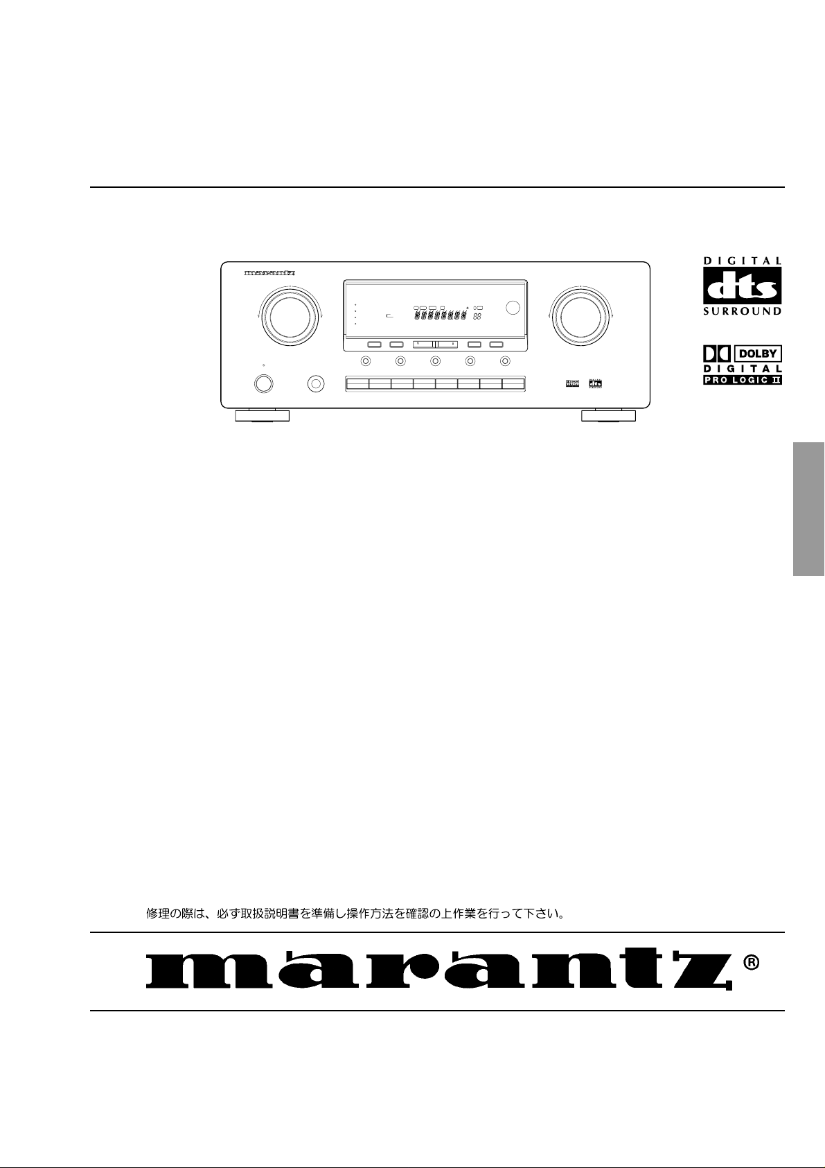
AV SURROUND RECEIVER SR4200
PHONES
NIGHT
2
DIGITAL PRO LOGIC
2
DTS
STEREO
RDS PTYRTRT TA TP
TAPE M
CDR/MD
MEMO
DELAY T.PRESET CH.
kHz
MHz
F/P
DIMMER MUTE
TAPE
TUNED
3 STEREO AC-3 PCM THEATER
ATT
HALL STADIUM DISCO CHURCH
VCR 1 REC SPK A B
DVD LD AUX SOURCE
PEAK
DISPLAY OFF
MEMORY
CLEAR
A/D
DVD
TV CD
TUNING/PRESET
SLEEP
S-DIRECT
DSS/VCR2
VCR1
TABLE OF CONTENTS
AV Surround Receiver
VOLUME
mS
MODE
DOWN
TUNER
UP
SR4200SR4200
Please use this service manual with referring to the user guide (D.F.U) without fail.
SR4200
319W855010 AO
3120 785 22690
First Issue:2001.08
Page 2
MARANTZ DESIGN AND SERVICE
Using superior design and selected high grade components, MARANTZ company has created the ultimate in stereo sound.
Only original
it is famous.
Parts for your
ORDERING PARTS :
Parts can be ordered either by mail or by Fax.. In both cases, the correct part number has to be specified.
The following information must be supplied to eliminate delays in processing your order :
1. Complete address
2. Complete part numbers and quantities required
3. Description of parts
4. Model number for which part is required
5. Way of shipment
6. Signature : any order form or Fax. must be signed, otherwise such part order will be considered as null and void.
MARANTZ parts can insure that your MARANTZ product will continue to perform to the specifications for which
MARANTZ equipment are generally available to our National Marantz Subsidiary or Agent.
USAUSA
MARANTZ AMERICA, INCMARANTZ AMERICA, INC.
1100 MAPLEWOOD DRIVE
ITASCA, IL. 60143
USA
PHONE : 630 - 741 - 0300
FAX : 630 - 741 - 0301
AMERICAS AMERICAS
SUPERSCOPE TECHNOLOGIES, INC.SUPERSCOPE TECHNOLOGIES, INC.
MARANTZ PROFESSIONAL PRODUCTS
2640 WHITE OAK CIRCLE, SUITE A
AURORA, ILLINOIS 60504 USA
PHONE : 630 - 820 - 4800
FAX : 630 - 820 - 8103
AUSTRALIAAUSTRALIA
QualiFi Pty Ltd,QualiFi Pty Ltd,
24 LIONEL ROAD,
MT. WAVERLEY VIC 3149
AUSTRALIA
PHONE : +61 - (0)3 - 9543 - 1522
FAX : +61 - (0)3 - 9543 - 3677
NEW ZEALANDNEW ZEALAND
WILDASH AUDIO SYSTEMS NZWILDASH AUDIO SYSTEMS NZ
14 MALVERN ROAD MT ALBERT
AUCKLAND NEW ZEALAND
PHONE : +64 - 9 - 8451958
FAX : +64 - 9 - 8463554
EUROPE / TRADING EUROPE / TRADING
MARANTZ EUROPE B.V.MARANTZ EUROPE B.V.
P.O.BOX 80002, BUILDING SFF2
5600 JB EINDHOVEN
THE NETHERLANDS
PHONE : +31 - 40 - 2732241
FAX : +31 - 40 - 2735578
AUSTRALIA AUSTRALIA
TECHNICAL AUDIO GROUP PTY, LTDTECHNICAL AUDIO GROUP PTY, LTD
558 DARLING STREET,
BALMAIN, NSW 2041,
AUSTRALIA
PHONE : 61 - 2 - 9810 - 5300
FAX : 61 - 2 - 9810 - 5355
THAILANDTHAILAND
MRZ STANDARD CO.,LTDMRZ STANDARD CO.,LTD
746 - 754 MAHACHAI ROAD.,
WANGBURAPAPIROM, PHRANAKORN,
BANGKOK, 10200 THAILAND
PHONE : +66 - 2 - 222 9181
FAX : +66 - 2 - 224 6795
TAIWANTAIWAN
PAI- YUING CO., LTD.PAI- YUING CO., LTD.
6 TH FL NO, 148 SUNG KIANG ROAD,
TAIPEI, 10429, TAIWAN R.O.C.
PHONE : +886 - 2 - 25221304
FAX : +886 - 2 - 25630415
BRAZILBRAZIL
PHILIPS DA AMAZONIA IND. ELET. ITDAPHILIPS DA AMAZONIA IND. ELET. ITDA
CENTRO DE INFORMACOES AO
CEP 04698-970
SAO PAULO, SP, BRAZIL
PHONE : 0800 - 123123
FAX : +55 11 534. 8988
(Discagem Direta Gratuita)
CANADACANADA
LENBROOK INDUSTRIES LIMITEDLENBROOK INDUSTRIES LIMITED
633 GRANITE COURT,
PICKERING, ONTARIO L1W 3K1
CANADA
PHONE : 905 - 831 - 6333
FAX : 905 - 831 - 6936
SINGAPORESINGAPORE
WO KEE HONG DISTRIBUTION PTE LTDWO KEE HONG DISTRIBUTION PTE LTD
130 JOO SENG ROAD
#03-02 OLIVINE BUILDING
SINGAPORE 368357
PHONE : +65 858 5535 / +65 381 8621
FAX : +65 858 6078
MALAYSIAMALAYSIA
WO KEE HONG ELECTRONICS SDN. BHD.WO KEE HONG ELECTRONICS SDN. BHD.
SUITE 8.1, LEVEL 8, MENARA GENESIS,
NO. 33, JALAN SULTAN ISMAIL,
50250 KUALA LUMPUR, MALAYSIA
PHONE : +60 3 - 2457677
FAX : +60 3 - 2458180
JAPANJAPAN
MARANTZ JAPAN, INC.MARANTZ JAPAN, INC.
Technical
35- 1, 7- CHOME, SAGAMIONO
SAGAMIHARA - SHI, KANAGAWA
JAPAN 228-8505
PHONE : +81 42 748 1013
FAX : +81 42 741 9190
KOREAKOREA
MK ENTERPRISES LTD.MK ENTERPRISES LTD.
ROOM 604/605, ELECTRO-OFFICETEL, 16-58,
3GA, HANGANG-RO, YONGSAN-KU, SEOUL
KOREA
PHONE : +822 - 3232 - 155
FAX : +822 - 3232 - 154
SHOCK, FIRE HAZARD SERVICE TEST :
CAUTION : After servicing this appliance and prior to returning to customer, measure the resistance between either primary AC
cord connector pins ( with unit NOT connected to AC mains and its Power switch ON ), and the face or Front Panel of product and
controls and chassis bottom.
Any resistance measurement less than 1 Megohms should cause unit to be repaired or corrected before AC power is applied, and
verified before it is return to the user/customer.
Ref. UL Standard No. 1492.
In case of difficulties, do not hesitate to contact the Technical
Department at above mentioned address.
010620 A.O
Page 3

1. TECHNICAL SPECIFICATIONS
FM TUNER SECTION
Frequency Range......................................................................................................................................
87.5 - 108.0 MHz (K, /L, /N, /U)
Usable Sensitivity ..................................................................................................................................... IHF 1.8 V/16.4 dBf
Signal to Noise Ratio........................................................................................................................... Mono/Stereo 70/65 dB
Distortion ............................................................................................................................................. Mono/Stereo 0.2/0.3 %
Stereo Separation ................................................................................................................................................ 1 kHz 45 dB
Alternate Channel Selectivity ........................................................................................................................ 300 kHz 60 dB
Image Rejection ........................................................................................................................................... 82 MHz 70 dB (F)
98 MHz 70 dB (K, /L, /N, /U)
Tuner Output Level..................................................................................................................... 1 kHz, 40 kHz Dev 600 mV
AM TUNER SECTION
Frequency Range.............................................................................................................................
LW: 152 - 282 kHz, MW: 531 - 1602 kHz kHz (N)
Signal to Noise Ratio....................................................................................................................................................... 50 dB
Usable Sensitivity ............................................................................................................................................. Loop 400 V/m
Distortion ......................................................................................................................................... 400 Hz, 30 % Mod. 0.5 %
Selectivity ......................................................................................................................................................... 18 kHz 60 dB
AUDIO SECTION
Continuous Power Output (8 ohms / 20 Hz - 20 kHz)
Front ........................................................................................................................................................................... 70W
Center ......................................................................................................................................................................... 70W
Surround ..................................................................................................................................................................... 70W
THD Front (20 Hz - 20 kHz) ............................................................................................................................. 8 ohms 0.09 %
Input Sensitivity/Impedance
Linear................................................................................................................................................... 316 mV/ 47 Kohms
Signal to Noise Ratio
Linear......................................................................................................................................................................... 99 dB
76.0 - 90.0 MHz (F)
531 - 1602 kHz (F, /K, /L)
520 - 1710 kHz (U)
VIDEO
Input Level/Impedance ................................................................................................................................... 1 Vp-p/ 75 ohms
Output Level/Impedance ................................................................................................................................ 1 Vp-p/ 75 ohms
GENERAL
Power Requirement...........................................................................................................................
Power Consumption .................................................................................................................................................
Dimension (MAX)
Width............................................................................................................................................. 17-3/8 inches (440 mm)
Height ............................................................................................................................................ 6-1/2 inches (164 mm)
Depth ............................................................................................................................................ 14-3/8 inches (365 mm)
Weight...................................................................................................................................................... 21.4 lbs (9.7 Kg)
AC 100 V 50/60 Hz (F)
AC 220 V 50 Hz (K)
AC 110 V 60 Hz (L)
AC 230 V 50 Hz (N)
AC 120 V 60 Hz (U)
280W (K, /N)
ACCESSORIES
Remote Control Unit RC5200SR ............................................................................................................................................ 1
AAA-size batteries .................................................................................................................................................................. 2
FM Lead Type Antenna (N, /K, /L).......................................................................................................................................... 1
FM Feader Antenna (U, /F) .................................................................................................................................................... 1
FM Antenna Converter (U, /F) ................................................................................................................................................ 1
AM Loop Antenna ................................................................................................................................................................... 1
Warranty Card (U, /F) ............................................................................................................................................................. 1
Registration Card (N).............................................................................................................................................................. 1
User Guide ............................................................................................................................................................................. 1
AC Power Cord (N)................................................................................................................................................................. 1
Post Card (F) .......................................................................................................................................................................... 1
170W (F)
320W (L)
2.7A (U)
Specifications subject to change without prior notice.
1
Page 4
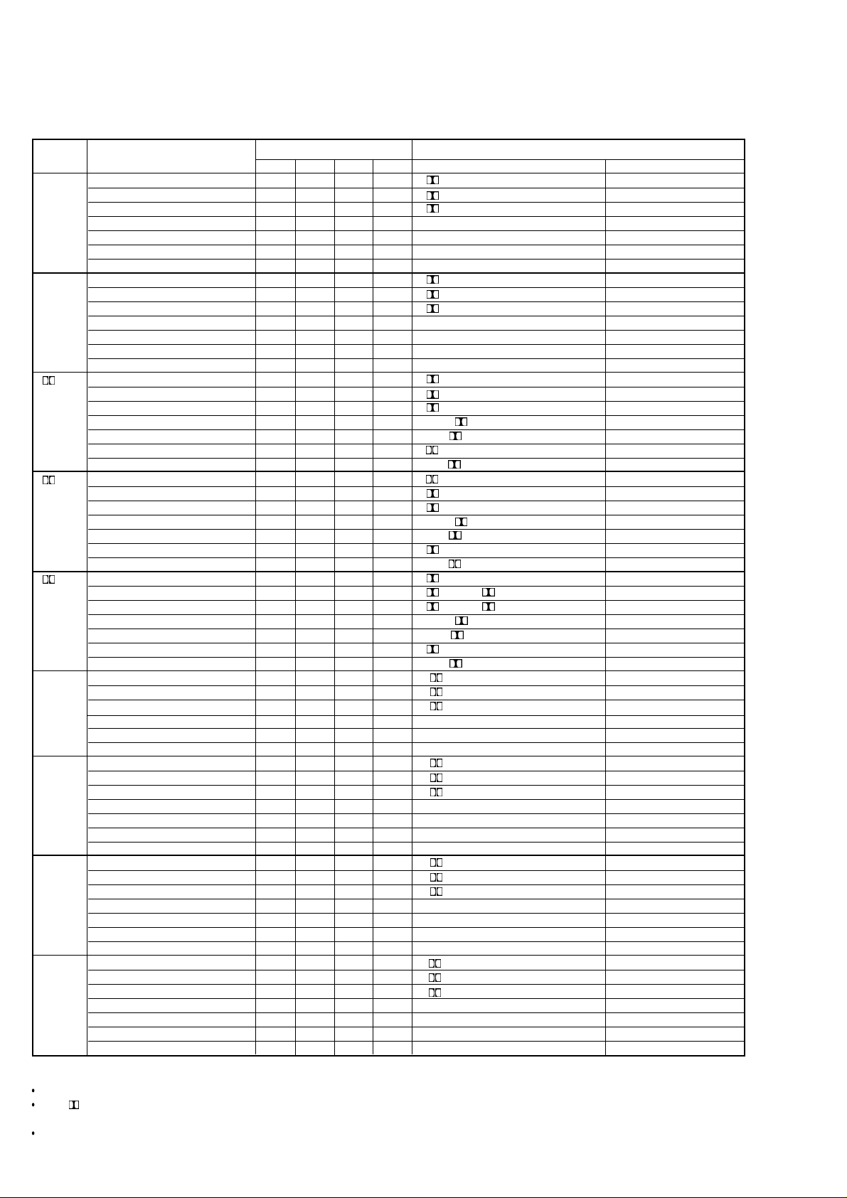
2. REMARK
The relation between the selected surround mode and the input signal
The surround mode is selected with the surround mode b uttons of the SR4200 or the remote control unit. However, the sound from the speakers
depend upon the relationship between the selected surround mode and the input signal. They are as follows;
SURROUND
MODE L/R LS/RS C SW FORMAT STATUS & SURROUND MODE
AUTO DOLBY DIGITAL(5.1CH)
STEREO DOLBY DIGITAL(5.1CH)
MOVIE DOLBY DIGITAL(2CH)
MUSIC DOLBY DIGITAL(2CH)
PRO LOGIC DOLBY DIGITAL(2CH)
DTS DOLBY DIGITAL(5.1CH)
MOVIE DOLBY DIGITAL(5.1CH)
HALL DOLBY DIGITAL(2CH)
MATRIX DOLBY DIGITAL(2CH:Lt/Rt)
GAME
VIRTUAL DOLBY DIGITAL(5.1CH)
5-STEREO DOLBY DIGITAL(5.1CH)
INPUT SIGNAL
DOLBY DIGITAL(2CH)
DOLBY DIGITAL(2CH:Lt/Rt)
96KHZ PCM
PCM(AUDIO)
ANALOG
DTS(5.1CH)
DOLBY DIGITAL(2CH)
DOLBY DIGITAL(2CH:Lt/Rt)
96KHZ PCM
PCM(AUDIO)
ANALOG
DTS(5.1CH)
DOLBY DIGITAL(5.1CH)
DOLBY DIGITAL(2CH:Lt/Rt)
96KHZ PCM
PCM(AUDIO)
ANALOG
DTS(5.1CH)
DOLBY DIGITAL(5.1CH)
DOLBY DIGITAL(2CH:Lt/Rt)
96KHZ PCM
PCM(AUDIO)
ANALOG
DTS(5.1CH)
DOLBY DIGITAL(5.1CH)
DOLBY DIGITAL(2CH:Lt/Rt)
96KHZ PCM
PCM(AUDIO)
ANALOG
DTS(5.1CH)
DOLBY DIGITAL(2CH)
DOLBY DIGITAL(2CH:Lt/Rt)
96KHZ PCM
PCM(AUDIO)
DTS(5.1CH)
96KHZ PCM
PCM(AUDIO)
ANALOG
DTS(5.1CH)
DOLBY DIGITAL(2CH)
DOLBY DIGITAL(2CH:Lt/Rt)
96KHZ PCM
PCM(AUDIO)
ANALOG
DTS(5.1CH)
DOLBY DIGITAL(2CH)
DOLBY DIGITAL(2CH:Lt/Rt)
96KHZ PCM
PCM(AUDIO)
ANALOG
DTS(5.1CH)
OOOO
O––O
OOOO
O–––
O––O
O––O
OOOO
O––O
O––O
O––O
O–––
O––O
O––O
O––O
OOOO
OOOO
OOOO
––––
OOOO
OOOO
––––
OOOO
OOOO
OOOO
––––
OOOO
OOOO
––––
OOOO
OOOO
OOOO
––––
OOOO
OOOO
––––
––––
––––
––––
––––
––––
OOOO
––––
––––
––––
––––
OOOO
OOOO
––––
––––
––––
––––
––––
O––O
O––O
––––
OOOO
OOOO
OOOO
––––
OOOO
OOOO
OOOO
OUTPUT FLUORESCENT INDICATOR
DIGITAL, AUTO
>AUTO>
DIGITAL, AUTO
DIGITAL, MOVIE, AUTO
PCM, STERE, AUTO
PCM, STERE, AUTO
STEREO, AUTO >AUTO>
dts, AUTO >AUTO>
DIGITAL,STEREO >STEREO>
DIGITAL,STEREO
DIGITAL,STEREO
PCM, STEREO >STEREO>
PCM, STEREO >STEREO>
STEREO >STEREO>
dts , STEREO >STEREO>
DIGITAL >DOLBY D>
DIGITAL, MOVIE
DIGITAL, MOVIE
(PCM), , MOVIE
PCM, , MOVIE
, MOVIE
(dts), , MOVIE
DIGITAL >DOLBY D>
DIGITAL, MUSIC
DIGITAL, MUSIC
(PCM), , MUSIC
PCM, , MUSIC
, MUSIC
(dts), , MUSIC
DIGITAL >DOLBY D>
DIGITAL, PRO LOGIC >DOLBY PL>
DIGITAL, PRO LOGIC >DOLBY PL>
(PCM), PRO LOGIC >DOLBY PL>
PCM, PRO LOGIC >DOLBY PL>
PRO LOGIC >DOLBY PL>
(dts), PRO LOGIC >DOLBY PL>
( ), dts >DTS>
( ), dts >DTS>
( ), dts >DTS>
(PCM), dts
(PCM), dts >DTS>
dts >DTS>
( ), DSP, MOVIE/ HALL/ MATRIX/ GAME >MOVIE/ HALL/ MATRIX/ GAME>
( ), DSP, MOVIE/ HALL/ MATRIX/ GAME >MOVIE/ HALL/ MATRIX/ GAME>
( ), DSP, MOVIE/ HALL/ MATRIX/ GAME >MOVIE/ HALL/ MATRIX/ GAME>
(PCM), DSP, MOVIE/ HALL/ MATRIX/ GAME >MOVIE/ HALL/ MATRIX/ GAME>
PCM, DSP, MOVIE/ HALL/ MATRIX/ GAME >MOVIE/ HALL/ MATRIX/ GAME>
DSP, MOVIE/ HALL/ MATRIX/ GAME >MOVIE/ HALL/ MATRIX/ GAME>
(dts),DSP, MOVIE/ HALL/ MATRIX/ GAME >MOVIE/ HALL/ MATRIX/ GAME>
( ), DSP, VIRTUAL >VIRTUAL>
( ), DSP, VIRTUAL >VIRTUAL>
( ), DSP, VIRTUAL >VIRTUAL>
(PCM), DSP , VIRTUAL >VIRTUAL>
PCM, DSP , VIRTUAL >VIRTUAL>
DSP, VIRTUAL >VIRTUAL>
(dts),DSP, VIR TUAL >VIRTUAL>
(PCM)
PCM
dts >5-STEREO>
TEMPORARY DISPLAY STATUS
>AUTO>
>AUTO>
>AUTO>
>AUTO>
>STEREO>
>STEREO>
>DOLBY PLII>
>DOLBY PLII>
>DOLBY PLII>
>DOLBY PLII>
>DOLBY PLII>
>DOLBY PLII>
>DOLBY PLII>
>DOLBY PLII>
>DOLBY PLII>
>DOLBY PLII>
>DOLBY PLII>
>DOLBY PLII>
>DTS>
>5-STEREO>
>5-STEREO>
>5-STEREO>
>5-STEREO>
>5-STEREO>
>5-STEREO>
Note:
Dolby Digital (2 ch: Lt/Rt): signal with Dolby Surround flag Speakers are full set.
When , dts or PCM is blinking, the selected surround mode is unavailable for
input signal. Select the other appropriate surround mode to playback.
No sound outputs from the surround speaker , center speaker and subwoofer if
the DVD disc has no surround data.
L/R : Front speaker
LS/RS : Surround speaker
C : Center speaker
SW : Sub woofer speaker
2
( ): The indicator blinks
Page 5
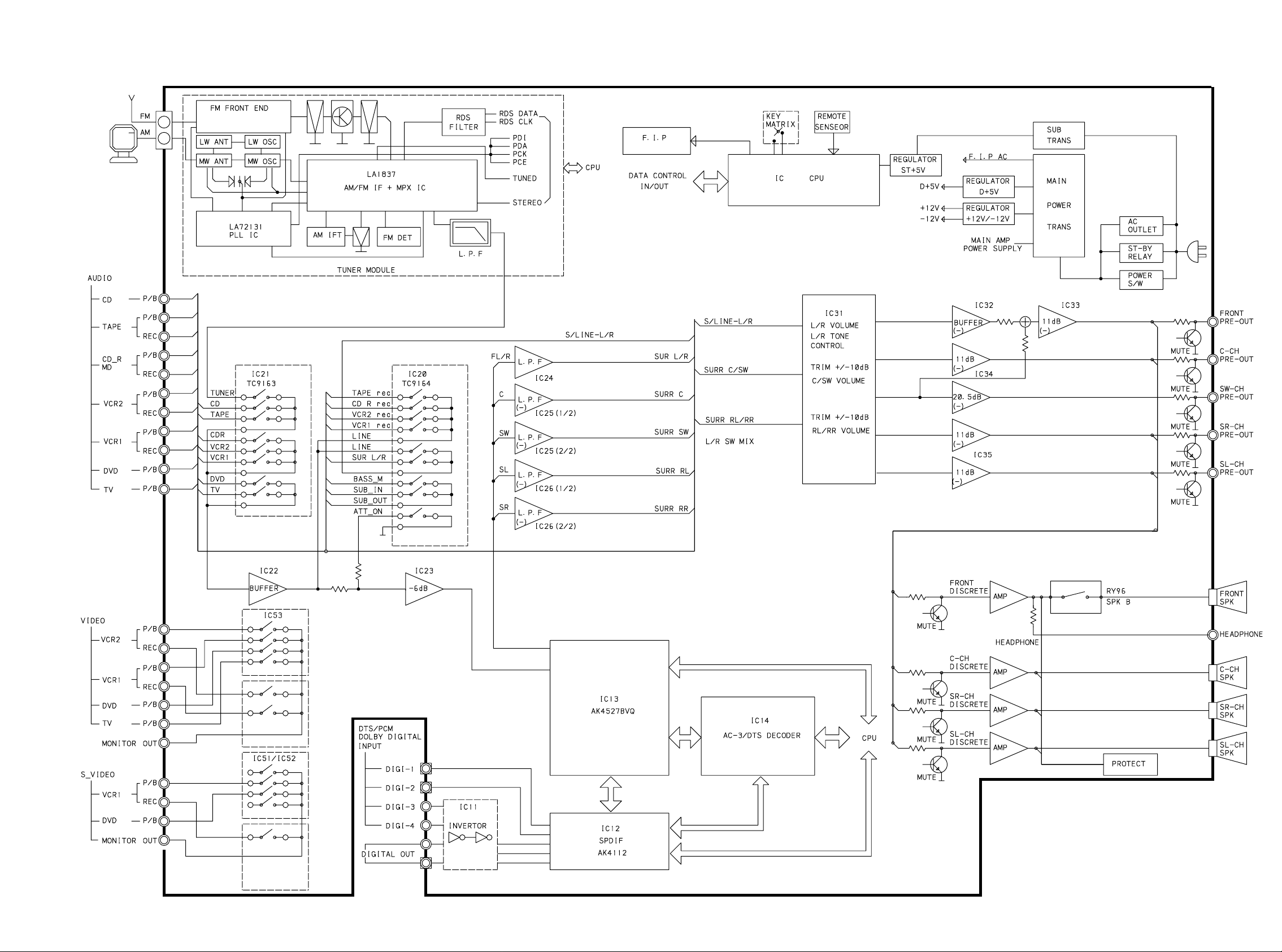
3. BLOCK DIAGRAM
3 4
Page 6
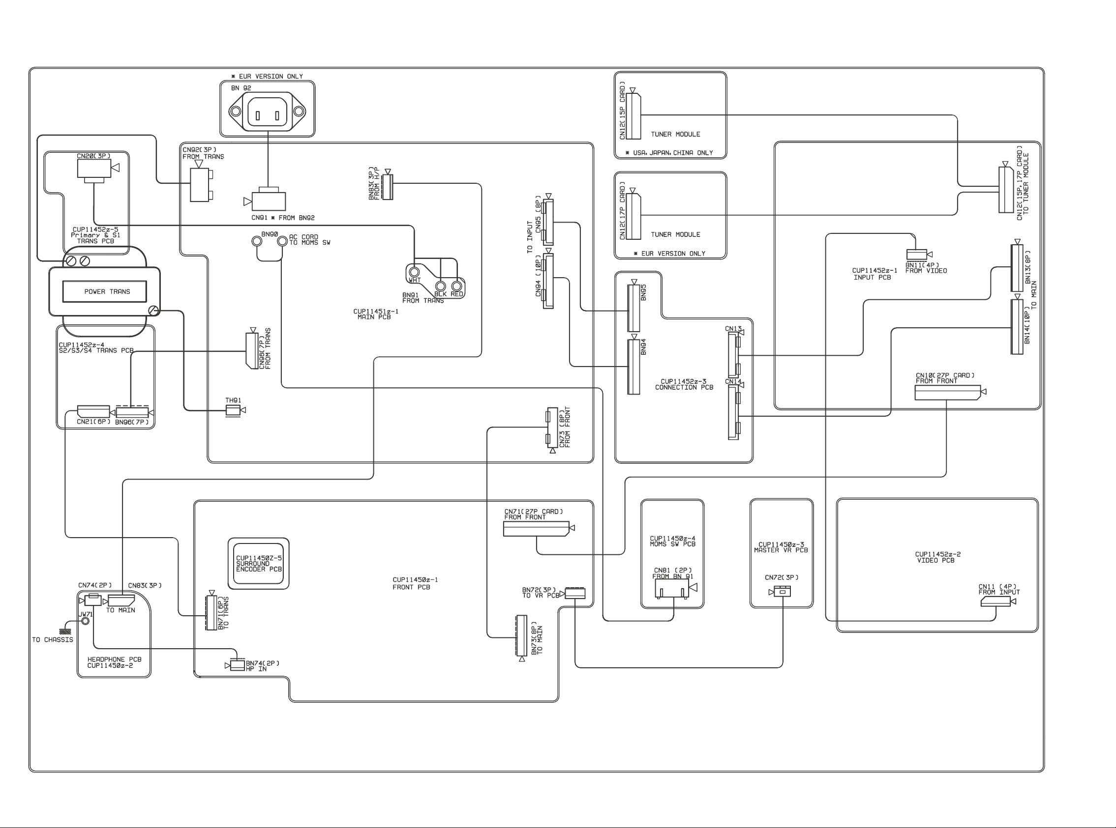
4. WIRIMG DIAGRAM
5 6
Page 7
5. SCHEMATIC DIAGRAM AND PARTS LOCATIONS (Parts Side)
FRONT PCB
7
8
Page 8
INPUT PCB
VIDEO PCB
9 10
Page 9

MAIN PCB
11 12
Page 10

POWER-2 PCB
POWER-1 PCB
CONNECTION PCB
13 14
Page 11

FRONT PCB
Q701 IC72 IC71 Q708 Q704 Q709
Q703
Q705
Q702
Q707
Q706
POWER PCB (F, /U)
MOMS PCB (K, /L, /N)
MASTER VR PCB
HEADPHONE JACK PCB
15 16
Page 12

INPUT PCB
IC11
IC12
IC14 IC13 IC23Q102 Q101
IC24
IC25
IC26
IC20
IC31
IC32
IC34
IC35IC22 IC21 IC33
Q511
Q509
IC51 IC52
Q514
Q515
Q513
IC53
Q512
VIDEO PCB
POWER-1 PCB
Q502
Q504
Q505
Q503
Q506
Q507
POWER-2 PCB
CONNECTION PCB
Q401
17 18
Page 13

MAIN PCB
Q901 IC95
Q584
Q624 Q629
Q544 Q972
Q559 Q519
Q514 Q564
Q581
Q621
IC91IC93 IC92 Q951 Q952 Q943 Q942 Q939 Q938
Q541
Q556 Q516
Q969
Q511 Q561
Q626 Q623 Q628 Q622 Q627 Q625 Q630
Q583 Q558 Q518
Q543Q954 Q971
Q513 Q563 Q582 Q557 Q517
Q992 Q991
Q544 Q970
Q806 Q805 Q804 Q803 Q802 Q801
Q935 Q940
Q544 Q973
Q512 Q562 Q585 Q560 Q520
Q515 Q565
Q644
Q660 Q614
Q649
Q664
Q656
Q657 Q611
Q646
Q661
Q643
Q659 Q613
Q663
Q648
Q642 Q647 Q645 Q650
Q658 Q612 Q662 Q670 Q615 Q665
19 20
Page 14

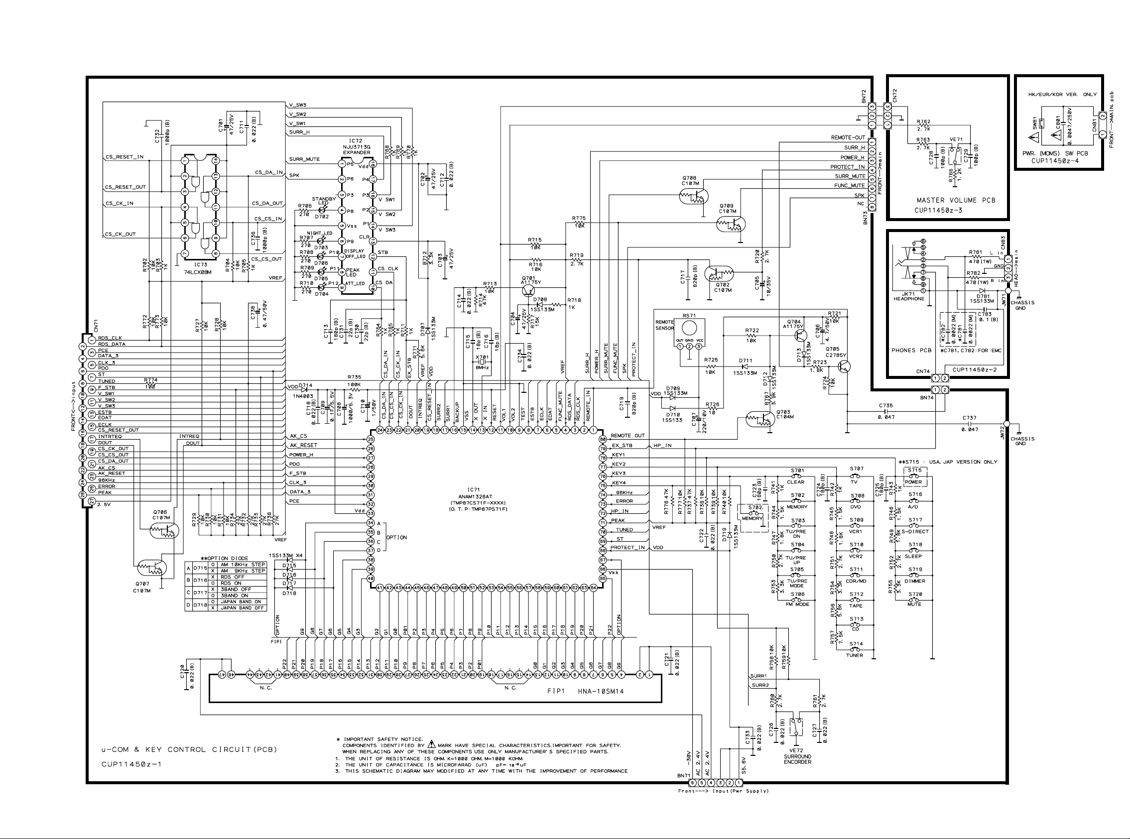
6. MICROPROCESSOR AND IC DATA
IC71 : ANAM1328AT
BLOCK DIAGRAM
Clock
Output Ports
P87
to
P80
P8
Flags
Time Base
P07
P00
Power Supply
VFT Power
Supply
Reset I/O
Test Pin
Resonator
connecting
Pins
VDD
VSS
VKK
RESET
TEST
XIN
XOUT
I/O Ports
P97
to
P90
P9
ALU
System Controller
Standby Controller
Timing Generator
High
frequ.
Generator
Low
frequ.
P2
P22
to
P20
PIN CONFIGURATION
(SIS) P97
VKK
(KEY0) P40
(KEY1) P41
(KEY2) P42
(KEY3) P43
(KEY4) P44
(KEY5) P45
(CIN5/KEY6) P46
(CIN4/KEY7) P47
(CIN3) P50
(CIN2) P51
(CIN1) P52
(CIN0) P53
P54
(PWM/PDO) P55
I/O Ports
P77
to
P70
P7
VFT drive circuit (automatic display)
Stack PointerP S W
RBS
Interrupt Controller
Timer
16-bit
Timer/Counters
TC1 TC2 TC3 TC4 SIO HSO
Watchdog
Timer
P0
to
P1
P17
to
P10
I/O Ports
P96 (S14)
P95 (S13)
P94 (S12)
P93 (S11)
P92 (S10)
P91 (S9)
P90 (S8)
P87 (S7)
P86 (S6)
P85 (S5)
P84 (S4)
P83 (S3)
P82 (S2)
P81 (S1)
P80 (S0)
P77 (G0)
P76 (G1)
P67
to
P60
P6
Data Memory
(RAM)
Register banks
8-bit
Timer/Counters
P75 (G2)
P74 (G3)
P73 (G4)
P72 (G5)
P71 (G6)
P70 (G7)
P67 (G8)
Program counter
Program Memory
Serial
Interfaces
P3
P37
to
P30
P66 (G9)
P65 (G10)
P64 (G11)
P63 (G12)
P62 (G13)
P61 (G14)
P60 (G15)
VDD
P07
P06
P05
P04
P03
P02
P01
P00
(ROM)
Register
Decoder
6-bit A/D
Converter
P5
P55
to
P50
Key scan
control
Inst.
Inst.
P4
P47
to
P40
PIN FUNCTIONS
PIN No. SYMBOL I/O DESCRIPTION
1,2 REMOTE IN I Remote Control Sensor Data Input
3 RDS CLK I/O
RDS IC (on the Tuner Module) CLK/Data Port
4 RDS DA TA I/O
5 Function Mute O Function Mute Control Output Port(Active "H")
6 E. VOL. Data O
7 E. VOL. CLK O Electronic Vol.IC (M62446FP) Data/CLK/STB Port
8 E. VOL. CE(STB) O
9 Vpp(Test) - Program Supply Voltage (GND Connection)
10 Volume Up(Encoder) I
Master Volume Up/Down Control Port
11 Volume Down(Encoder) I
12 RESET I Reset Input Port("L")
13 XIN I 8MHz Cystal Connection Port
14 X OUT
O
15 Vss(GND) I Divice GND Port
16 Back Up I Back Up Mode Control Port ("L")
17 SURROUND SW I Surround mode (ENCODER) Control Port
18 SURROUND SW I
19 CS RESET IN O Reset (Initial Clear) Control Port for CS493263
20 INTREQ I Interrupt Requst Input Port for CS493263
21 D OUT I Data Input Port for CS493263/AK4112VF
22 CS CLK IN O CLK Output Port for NJU3713G/CS493263/AK4527BVQ
23 CS CS IN O Chip Selector Port for CS493263
24 CS DA IN O Data Output Port for NJU3713G/CS493263/AK4527BVQ
25 AK CS O Chip Selector Port for AK4527BVQ
26 AK RESET O Reset Port for AK4527BVQ/AK4112VF
27 POWER " H " O Power Relay On/Off Control Port(Active"H")
28 PDO I PLL IC(LC72131)Data Input Port
29 FUNC.STB O Function IC(TC9163/64) Strobe Control Port
30 CLK3 O Function/PLL IC CLK Control Port
31 DATA3 O Function/PLL IC Data Control Port
32 PCE O PLL IC(LC72131:on the Tuner Module) Chip Enable Control Port
33 VDD/VCC - Power Supply Port (+5V)
34~37 Option O Option Control Output Port
34~43 FIP Grid O FIP Grid Control Port
44~65 FIP Segment O FIP Segment Control Port
66
Vkk
- FIP Power Supply Port (-30V)
67 Option I Option Control Input Port
68 Protect IN I Protect Input Port(Active " L " )
69 Stereo IN I Stereo Display Control Port
70 Tuned IN I Tuned Display Control Port
71 PEAK O Peak Level Control Input Port
72 HP IN I Headphon Detective Input Port(Active " H ")
73 ERROR I Error Detection Input Port
74 96KHz I 96KHz Detection Input Port
75~78 KEY Matrix I Key Control Input Port
79 EX STB O Expended IC(NJU3713G) Strobe Control Port
80 Bus Out O Remote Control Data Output Port
(INT1) P11
(INT0) P10
(DVO) P13
(INT2/TC1) P12
TEST
(XTIN) P21
(XTIN) P22
XIN
XOUT
RESET
VSS
(TC4) P31
(INT3/TC3) P30
(INTS/STOP) P20
(SI) P33
(SO) P34
(SCK) P32
(HSCK) P35
P36
(HSO) P37
P14
P16
(TC2) P15
P17
21 22
Page 15

IC13 : AK4527BVQ
BLOCK DIAGRAM
LIN+
LIN-
RIN+
RIN-
LOUT1
ROUT1
LOUT2
ROUT2
LOUT3
ROUT3
LPF DAC DATT
LPF DAC DATT
LPF DAC DATT
LPF DAC DATT
LPF DAC DATT
LPF DAC DATT
ADC HPF
ADC
HPF
[Serial Control Mode]
PIN CONFIGURATION
LOOP1
LOOP0/SDA/CDTI
DIF1/SCL/CCLK
SDOS
I2C
SMUTE
BICK
LRCK
SDTI1
SDTI2
SDTI3
SDTO
DAUX
DFS
4443424140393837363534
1
2
3
4
5
6
7
8
9
10
11
12NC
131415161718192021
DZFE
TVDD
Audio
I/F
MCLK
LRCK
BICK
SDOUT
SDIN1
SDIN2
SDIN3
DIF0/CSN
P/S
MCLK
DZF1
AK4527BVQ
Top View
DVDD
DVSS
PDN
TSTNCADIF
Format
Converter
AVSS
AVDD
VREFH
VCOM
33
32
31
30
29
28
27
26
25
24
23
22
CAD1
CAD0
MCLK
LRCK
BICK
DAUX
SDOS
SDTO
SDTI1
SDTI2
SDTI3
DZF2/OVF
RIN+
RINLIN+
LINROUT1
LOUT1
ROUT2
LOUT2
ROUT3
LOUT3
RX1 RX2RX3 RX4
XTI
XTO
MCLK
DIR
AK4112A
LRCK
BICK
SDTO
LRCK
BICK
AC3
SDIN
SDOUT1
SDOUT2
SDOUT3
PIN FUNCTIONS
PIN No. Pin Name I/O Function
1 SDOS I SDTO Source Select Pin (Note 1)
2 12C I Control Mode Select Pin
3 SMUTE I Soft Mute Pin (Note 1)
4 BICK I Audio Serial Data Clock Pin
5 LRCK I Input Channel Clock Pin
6 SDTI1 I DAC1 Audio Serial Data Input Pin
7 SDTI2 I DAC2 Audio Serial Data Input Pin
8 SDTI3 I DAC3 Audio Serial Data Input Pin
9 SDTO O Audio Serial Data Output Pin
10 DAUX I AUX Audio Serial Data Input Pin
11 DFS I Double Speed Sampling Mode Pin (Note 1)
12 NC - No Connect
13 DZFE I Zero Input Detect Enable Pin
14 TVDD - Output Buffer Power Supply Pin, 2.7V~5.5V
15 DVDD - Digital Power Supply Pin, 4.5V~5.5V
16 DVSS - Digital ground Pin, 0V
17 PDN I Power-Down & Reset Pin
18 TST I Test Pin
19 NC - No Connect
20 ADIF I Analog Input Format Select Pin
21 CAD1 I Chip Address 1 Pin
22 DAD0 I Chip Address 0 Pin
23 LOUT3 O DAC3 Lch Analog Output Pin
24 ROUT3 O DAC3 Rch Analog Output Pin
25 LOUT2 O DAC2 Lch Analog Output Pin
26 ROUT2 O DAC2 Rch Analog Output Pin
27 LOUT1 O DAC1 Lch Analog Output Pin
28 ROUT1 O DAC1 Rch Analog Output Pin
29 LIN- I Lch Analog Negative Input Pin
30 LIN+ I Lch Analog Positive Input Pin
31 RIN- I Rch Analog Negative Input Pin
32 PIN+ I Rch Analog Posivive Input Pin
33 DZF2 O Zero Input Detect 2 Pin (Note2)
OVF O Analog Input Overflow Detect Pin (Note 3)
34 VCOM O Common Voltage Output Pin, AVDD/2
35 VREFH I Positive Voltage Reference Input Pin, AVDD
36 AVDD - Analog Power Supply Pin, 4.5V~5.5V
37 AVSS - Analog Ground Pin, 0V
38 DZF1 O Zero Input Detect 1 Pin (Note 2)
39 MCLK I Master Clock Input Pin
40 P/S I Parallel/serial Select Pin
41 DIF0 I Audio Data Interface Format 0 Pin in parallel control mode
CSN I Chip Select Pin in 3-wire serial control mode
42 DIF1 I Audio Data Interface Format 1 Pin in parallel control mode
SCL/CCLK I Control Data Clock Pin in serial control mode
43 LOOP0 I Loopback Mode 0 Pin in parallel control mode
SDA/CDTI I/O Control Data Input Pin in serial control mode
44 LooP1 I Loopback Mode 1 Pin (Note 1)
Notes: 1. SDOS, SMUET, DFS, and LOOP pins are ORed with register data if P/S = L
2. The group 1 and 2 can be selected by DZFM2-0 bits fi P/S= L and DZFE= L .
3. This pin becomes OVF pin if OVFE bit is set to 1 at serial control mode.
4. All input pins should not be left floating.
L : Internal ADC output, H : DAUX input
2
L : 3-wire Serial, H : I
When this pin goes to H , soft mute cycle is initialized.
When returning to L , the output mute releases.
L : Normal Speed, H : Double Speed
No internal bonding.
L : mode 7(disable) at parallel mode,
zero detect mode is selectable by DZFM2-0 bits at aerial mode
H : mode 0(DZF1 is AND of all six channels)
When L ,the AK4527B is powered-down and the control registers are reset to default
state. If the state of P/S or CAD0-1 changes, then the AK4527B must be reset by PDN.
This Pin should be connected to DVSS.
No internal bonding.
H : Full-differential input, L : Single-ended input
When the input data of the group 1 folloW total 8192 LRCK cycles with 0 input
data, this pin goes to H .
This pin goes to H if the analog input of Lch or Rch is overflows.
Large external capacitor around 2.2 F is used to reduce power-supply noise.
When the input data of the group 1 follow total 8192 LRCK cycles with 0 input data,
this pin goes to H
L : Serial control mode, H : Parallel control mode
This Pin should be connected to DVDD at I
12C = L : CCLK (3-wire Serial), 12C = H : SDA (I
Enables digital loop-back from ADC to 3 DACs.
12C= L : CDT1 (3-wire Serial), 12C = H : SDA (I
Enables all 3 DAC channels to be input from SDTI1.
C Bus
2
C bus control mode
2
C Bus)
2
C Bus)
23 24
Page 16

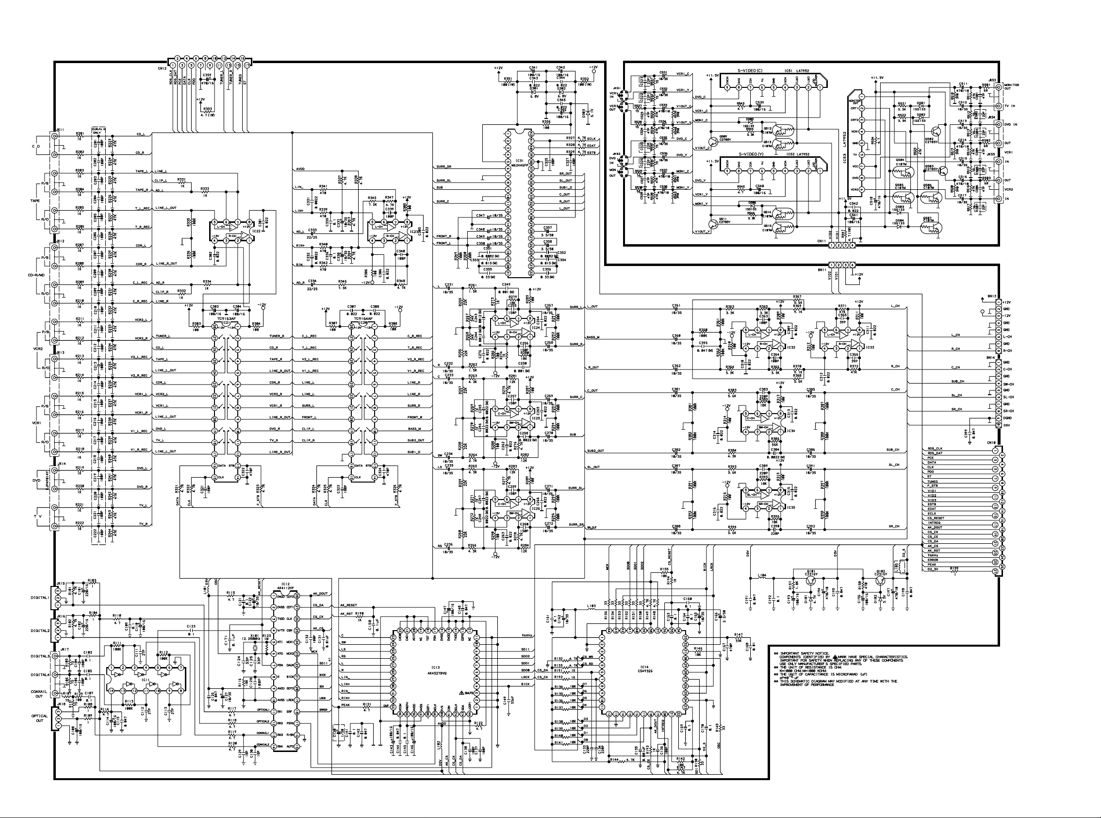
IC14 : CS493263
BLOCK DIAGRAM
RESET
CMPDAT
SDATAN2
CMPCLK
SCLKN2
CMPREQ
LRCLKN2
SCLKN1
STCCLK2
LRCLKN1
SDATAN1
CLKIN
CLKSEL
SCDIO,SCDOUT,PSEL,GPIO9
Compressed
Data Input
Interface
Digital
Audio
Input
Interface
FILTD FILTS VA AGND DGND(3:1) VD(3:1)
PIN CONFIGURATION
AUDATA3, XMT958
WR,DS,EMWR,GPIO10
RD,R/W,EMOE,GPIO11
DAT A7,EMAD7,GPIO7
DAT A6,EMAD6,GPIO6
DAT A5,EMAD5,GPIO5
DAT A4,EMAD4,GPIO4
DAT A3,EMAD3,GPIO3
DAT A2,EMAD2,GPIO2
DAT A1,EMAD1,GPIO1
DAT A0,EMAD0,GPIO0
ABOOT,INTREQ
EXTMEM,GPIO8
PLL
Clock Manager
VD1
DGND1
A1,SCDIN
A0,SCCLK
VD2
DGND2
CS
SDAT AN1
DATA7:0,
EMAD7:0,
GPIO7:0
Framer
Shifter
Input
Buffer
Controller
RAM Input
Buffer
WR,
RD,
R/W,
EMOE,
CS
GPIO11
6 5 4 3 2 1 44 43 42 41 40
7
8
9
10
11
12
13
14
15
16
17
18 19 20 21 22 23 24 25 26 27 28
DR,
EMWR,
GPIO10
DSP Processing
RAM
Program
Memory
ROM
Program
Memory
CS493XX-CL
44-pin PLCC
SCDIO,
SCDOUT,
PSEL,
GPIO9
Parallel or Serial Host Interface
24-Bit
RAM
Data
Memory
ROM
Data
Memory
STC
Top View
(TOP VIEW)
A0,
SCCLK
39
38
37
36
35
34
33
32
31
30
29
A800T
A1,
SCDIN
RAM
Output
Buffer
INTERQ
Output
Formatter
MCLK
SCLK
LRCLK
AUDATA0
AUDATA1
AUDATA2
DC
DD
RESET
AGND
VA
FILT1
FILT2
CLKSEL
CLKIN
CMPREQ,LRCLKN2
CMPCLK,SCLKN2
CMPDAT ,SCLKN2,RCV958
LRCLKN1
SCLKN1,STCCLK2
DGND3
VD3
EXTMEM.
GPIO8
DD
DC
MCLK
SCLK
LRCLK
AUDA
XMT95
PIN FUNCTIONS
1,12,23 VD1/2/3
2,13,24
3
DGND1/2/3 - Digtal ground
AUDATA 3/XMT958 O SPDIF transmitter output/Digital audio output (unused)
4
5
6
7
8
9
10
11
14
15
16
17
SCDIN I SPI Serial data input pin
SCCLK I Serial control clock input pin
DATA 7 I/O
DATA 6 I/O
DATA 5 I/O
DATA 4 I/O Serial data in/output pins
DATA 3 I/O
DATA 2 I/O
DATA 1 I/O
DATA 0 I/O
18
19
20
21
22
25
26
27
28
29
30
31
SCDOUT O Serial control port data output pin
INTREQ O Control port interrupt request output pin
GPIO 8 I/O General purpose in/output number 8 pin
SDATAN1 I PCM audio data input number 1 pin
SCLKN1 I PCM audio input bit clock pin
LRCLKN1 I PCM audio input sample rate clock pin
SDATAN1 I PCM audio data input number 2 pin
SCLKN2 I PCM audio input bit clock pin
LRCLKN2 I PCM audio input sample rate clock pin
CLKIN I Master clock input(used external clock)
CLKSEL I DSP clock mode select pin: connect the GND
32 FILT1
33
34
35 AGND
36
RESET I Master reset input pin
37
38
39
40
41
42
AUDATA 2 O PCM multi-format digital-audio data output2 pin
AUDATA 1 O PCM multi-format digital-audio data output1 pin
AUDATA 0 O PCM multi-format digital-audio data output0 pin
LRCLK I Audio output sample rate clock pin
43
44
NamePIN No. FUNCTION
I/O
- Digtal positive supplies. Nominally + 2.5V
WR I Host write strobe pin
RD I Host parallel output enable pin
CS I Host parallel chip select pin
Connects to an external filter for the on-chip phase-locked loop
FILT1 Connects to an external filter for the on-chip phase-locked loop
VA - Analog positive supply for clock generator. Nominally + 2.5V
- Analog ground supply for clock generator PLL.
DD - Reserved pin and should be pulled up with an external resister.
DC - Reserved pin and should be pulled up with an external resister.
SCLK I Audio output bit clock pin
MCLK I Audio master clock output pin
25 26
Page 17

IC12 : AK4112AVF
BLOCK DIAGRAM
PIN FUNCTIONS
RX1
RX2
RX3
RX4
V/TX
DVDD
DVSS
PDN
AVSS AVDD R MCKO1 XTI XTO
Input
Selector
System
Control
AC-3/MPEG
PIN CONFIGURATION
DVDD
DVSS
TVDD
V/TX
XTI
XTO
PDN
R
AVDD
AVSS
RX1
RX2/DIF0
RX3/DIF1
1
2
3
4
5
6
7
8
9
10
11
12
13
Clock
Recovery
DAIF
Decoder
Detect
AUTO
[Serial Control Mode]
TOP
VIEW
MCKO2
Clock
Generator
DEM
Error
Detect
ERF
27
26
25
24
23
22
21
20
19
18
17
16
28
X tal
Oscillator
96kHz
Detect
Audio
P/S="L"
CM0/CDTO
CM1/CDTI
OCKS1/CCLK
OCKS0/CSN
MCKO1
MCKO2
DAUX
BICK
SDTO
LRCK
ERF
FS96
P/SN
I/F
uP
I/F
FS96
DAUX
LRCK
BICK
SDTO
TVDD
CSN
CCLK
CDTO
CDTI
PIN No. Pin Name I/O Function
1 DVDD - Digital Power Supply Pin, 3.3V
2 DVSS - Digital Ground Pin
3 TVDD - Input Buffer Power Supply Pin, 3.3V or 5V
4 V O Validity Flag Output Pin in Parallel Mode
TX O Transmit channel (through data) Output Pin in Serial Mode
5 XTI I X tal Input Pin
6 XTO O X tal Output Pin
7 PDN I Power-Down Mode Pin
When L , the Ak4112A is powered-down and reset.
8 R - External Resistor Pin
18k +/-1% resistor and 100pF or less capacitor to AVSS externally.
9 AVDD -
10 AVSS - Analog Ground Pin
11 RX1 I Receiver Channel 1
12 DIF0 I Audio Data Interface Format 0 Pin in Parallel Mode
RX2 I Receiver Channel 2 in Serial Mode
13 DIF1 I Audio Data Interface Format 1 Pin in Parallel Mode
RX3 I Receiver Channel 3 in Serial Mode
14 DIF2 I Audio Data Interface Format 2 Pin in Parallel Mode
RX4 I Receiver Channel 4 in Serial Mode
15 AUTO O Non-PCM Detect Pin
16 P/S I Parallel/Serial Select Pin
17 FS96 O 96kHz Sampling Detect Pin
18 ERF O Unlock & Parity Error output Pin
19 LRCK I/O Output Channel Clock Pin
20 SDTO O Audio Serial Data Output Pin
21 BICK I/O Audio Serial Data Clock Pin
22 DAUX I Auxiliary Audio Data Input Pin
23 MCK02 O Master Clock #2 Output Pin
24 MCK01 O Master Clock #1 Output Pin
25 OCKS0 I Output Clock Select 0 Pin in Parallel Mode
CSN I Chip Select Pin in Serial Mode
26 OCKS1 I Output Clock Select 1 Pin in Parallel Mode
CCLK I Control Data Clock Pin in Serial Mode
27 CM1 I Master Clock Operation Mode Pin0 in Parallel Mode
CDTI I Control Data Input Pin in Serial Mode
28 CM0 I Master Clock Operation Mode Pin1 in Parallel Mode
CDTO O Control Data Output Pin in serial Mode
Note 1: All input pins except internal pull-down pins should not be left floating.
Analog Power Supply Pin
This channel is selected in Parallel Mode or default of Serial Mode.
L : No detect, H : Detect
L : Serial Mode, H : Parallel Mode
(RX Mode) H :fs=88.2kHz or more, L fs=54kHz or less.
(X tal Mode) H : XFS96-1, L : SF96=0.
L : NO Error, H : Error
RX4/DIF2
14
15
AUTO
27 28
Page 18

IC20 : TC9164AF
BLOCK DIAGRAM
2
L-S R-S
1
L-S
3
2
L-COM
L-COM
L-COM
L-COM
L-S
L-S
L-S
L-S
L-S
ST
4
1
5
3
6
4
7
2
8
5
9
6
10
3
11
7
12
4
13
Vss GND VDD
1
LEVEL SHIFTER
LATCH CIRCUIT
SHIFT REGISTER
14 28
LATCH CIRCUIT
LEVEL SHIFTER
IC22~26, 32~35 : LA6462
IC31 : M62446FP
BLOCK DIAGRAM
PIN FUNCITON
1. A OUTPUT
2. A-INPUT
3. A+INPUT
4. V
5. B+INPUT
6. B-INPUT
7. B OUTPUT
8. V
video switch
(4 input 1 output)
6dB
amp
8
7
B
6
5
control
1
27
1
R-S
26
2
R-COM
25
24
23
22
21
20
19
18
17
16
15
R-S
3
R-S
4
R-COM
R-S
5
R-S
6
R-COM
R-S
7
R-COM
DATA
CK
1
2
3
IC51~53 : LA7952
4
A
2
3
4
LA6462M/
LA6458M
driver
1
VIDEO OUT A B VIN1 GND VIN2 VCC VIN3 VIN4
23456789
OUT4
OUT3
OUT2
OUT1
AVDD
SWin
GNDS
SRin
SLin
GNDC
Cin
GNDR
Rin
GNDL
Lin
BYPASSR
BYPASSL
LTRE
LBASS3
LBASS2
LBASS1
DVDD
1
2
OUTPUT
PORT
3
4
5
6
7
8
9
10
11
12
13
14
15
16
17
18
19
20
21
tone tone
volume
volume
volume
volume
volume
volume
MCU I/F
42
41
40
39
38
37
36
35
34
33
32
31
30
29
28
27
26
25
24
23
22
CLK
DATA
LATCH
DGND
AGND
SWout
SRout
SLout
Cout
Rout
Lout
AVss
CL1
CL2
CR1
CR2
RTRE
RBASS3
RBASS2
RBASS1
IC21 : TC9163AF
BLOCK DIAGRAM
2
L-S R-S
1
L-S
3
2
L-COM
L-COM
L-COM
L-COM
L-S
L-S
L-S
L-S
L-S
ST
4
1
5
3
6
4
7
2
8
5
9
6
10
3
11
7
12
4
13
Vss GND VDD
1
LEVEL SHIFTER
LATCH CIRCUIT
SHIFT REGISTER
14 28
LATCH CIRCUIT
LEVEL SHIFTER
IC31 : PIN CONFIGURATION
C in
SW in
SL in
SR in
BYPASS1
27
1
R-S
26
2
R-COM
25
24
23
22
21
20
19
18
17
16
15
R-S
3
R-S
4
R-COM
R-S
5
R-S
6
R-COM
R-S
7
R-COM
DATA
CK
1
IC72 : NJU3713
BLOCK DIAGRAM
2
3
4
DATA
CLK
Shift Register
Latch Circuit
BYPASS2
L in
R in
P1
P2
P3
P4
P5
P11
P12
U-com
interface
LATCH DATA CLK
IC72 : PIN CONFIGURATION
P5
P6
P7
P8
Vss
P9
STB
CLR
Controller Circuit
P10
P11
P12
volume
tone
volume
1
2
3
4
5
6
7
8
9
18
17
16
15
14
13
12
11
10
DD
V
P4
P3
P2
P1
CLR
STB
CLK
DATA
Cout
SWout
SLout
SRout
Lout
Rout
29
30
Page 19

7. MEASUREMENTS AND ADJUSTMENTS
ALIGNMENT INSTRUCTIONS
EQUIPMENT NEEDED:
AM Signal Generator
FM Signal Generator
Oscilloscope
VTVM(AC, DC)
Test loop antenna (AM Adjustment)
Dummy antenna (FM Adjustment)
Distortion analyser
IMPORTANT
1. Check power-source voltage.
2. Set the function switch to band aligned.
3. Keep the signal input as low as possible to adjust accurately.
4. Modulation and modulation frequency.
Item
Band
AM 30% 400Hz
FM 400Hz
100% (75 kHz Dev.) [U/F/L/K]
Modulation Modulation frequency
100% (40 kHz Dev.) [N]
ADJUSTMENT POINT (Reference Schematic Diagram Tuner section)
FIP DISPLAY
DIGITAL PROLOGIC
3STEREO AC-3PCM THEATER
MOVE MUSIC HALL MATRIX
ARENA JAZZ GAME SP.
ANALOG PCM NIGHT AUTO
TUNER MODULE
ANODE CONNECTION
10G 9G 8G 7G 6G 5G 4G 3G 2G 1G
P1 AUTO d2 d2 d2 d2 d2 d2 d2 d2 kHz
P2 NIGHT d1 d1 d1 d1 d1 d1 d1 d1 1d
P3 PCM e e e e e e e e 1e
P4 ANALOG r r r r r r r r 1c
P5 JAZZ p p p p p p p p 1g
P6 GAME n n n n n n n n 1f
A
B
A : MW ANT COIL
B : LW ANT COIL (N Version)
G
C
H
FE
I
D
C : FM Stereo Separation Adj
D : AM Tuned LED Level Adj
E : FD
F : AM IF
G : FM Tuned LED Level Adj
H : Unused
I : FOR EUR
J : Others
(TOP VIEW)
J
P7 ARENA c c c c c c c c 1b
P8 SP. f f f f f f f f 1a
P9 A g g g g g g g g M
P10 B m m m m m m m m 2d
P11 MATRIX h h h h h h h h 2e
P12 HALL j j j j j j j j 2c
P13 MUSIC k k k k k k k k 2g
P14 MUVIE b b b b b b b b 2f
P15 VIRTUAL a2 a2 a2 a2
P16 COS a1 a1 a1 a1 a1 a1 a1 a1 2a
P17 DSP S1 S1 S1 S1 S1 S1 S1 S1
P18 STEREO S2 S2 S2 S2 S2 S2 S2 S2
P19 3 S3 S3 S3 S3 S3 S3 S3 S3 MEMO
P20 S4 S4 S4 S4 S4 S4 S4 S4 TAPE
P21 DIGITAL RDS Dp TA MHz
P22
PRO LOGIC
TUNED STEREO PTY RT TP mS
a2
a2 a2 a2 2b
DIGITAL
PRESET CH.
31 32
Page 20

1
WINDOW.FIP
2
VOLUME KNOB ASS’Y (B)
2
VOLUME KNOB ASS’Y (G)
3 U1B nsp POWER KNOB (B)
3
nsp POWER KNOB (G)
4
MARANTZ BADGE 185J251010
5N1B
FRONT PANEL
5
FRONT PANEL
5 U1B nsp FRONT PANEL
5
nsp FRONT PANEL
6 nsp SIDE BRACKET nsp
7
OPTICAL INDICATOR
8
FUNCTION KNOB (B)
8
FUNCTION KNOB (G)
9
SURROUND KNOB (B)
9
SURROUND KNOB (G)
10
TUNING KNOB (B)
10
TUNING KNOB (G)
11
JACK FOR HEADPHONE
12 nsp PCB BRACKET nsp
13 N1B
POWER PUSH KNOB (B)
13
POWER PUSH KNOB (G)
14
INDICATOR
15
/K1G
nsp POWER BRACKET nsp
16
nsp FRONT PCB ASS’Y nsp
16 U1B nsp FRONT PCB ASS’Y nsp
16 F1N nsp FRONT PCB ASS’Y nsp
16 K1G nsp FRONT PCB ASS’Y nsp
16 L1G nsp FRONT PCB ASS’Y nsp
17 nsp FIP SUPPORT nsp
18 nsp RUBBER CUSHION nsp
19
FOOT
20 nsp SUPPORT CUSHION nsp
21 nsp PCB HOLDER nsp
22 nsp BOTTOM CHASSIS nsp
23 nsp HEATSINK nsp
24
nsp TOP CABINET (B) nsp
24
nsp TOP CABINET (G) nsp
25 nsp PCB BRACKET nsp
26 nsp BRACKET PCB(H/T) nsp
27
/K1G
MAINS TRANSF. (N / K)
27
nsp MAINS TRANSF. (U / L)
27 F1N nsp MAINS TRANSF. (F)
28
nsp INPUT PCB ASS’Y nsp
28 U1B nsp INPUT PCB ASS’Y nsp
28 F1N nsp INPUT PCB ASS’Y nsp
28 K1G nsp INPUT PCB ASS’Y nsp
28 L1G nsp INPUT PCB ASS’Y nsp
29 nsp TR BRACKET nsp
30 nsp PCB BRACKET nsp
31 nsp VIDEO PCB nsp
32
nsp MAIN PCB ASS’Y nsp
32 U1B nsp MAIN PCB ASS’Y nsp
32 F1N nsp MAIN PCB ASS’Y nsp
32 K1G nsp MAIN PCB ASS’Y nsp
32 L1G nsp MAIN PCB ASS’Y nsp
33
nsp TUNER MODULE (F / K)
33
nsp TUNER MODULE (L / U)
33
TUNER MODULE (N)
34 N1B nsp REAR PANEL (N1B) nsp
34 N1G nsp REAR PANEL (N1G) nsp
34 U1B nsp REAR PANEL (U1B) nsp
34 F1N nsp REAR PANEL (F1N) nsp
34 L1G nsp REAR PANEL (L1G) nsp
34 K1G nsp REAR PANEL (K1G) nsp
35 nsp BUSHING FOR AC CORD nsp
36
MAINS CORD (N)
36
nsp MAINS CORD (U / L)
36 F1N nsp MAIINS CORD (F)
36 K1G nsp MA NS CORD (K)
37
AC RECEPTACLE (N)
37
/U1B
nsp AC OUTLET (F / L / U)
S1 nsp SCREW nsp
S2 nsp SCREW nsp
S3 nsp SCREW nsp
S4
nsp SCREW nsp
S4
nsp SCREW nsp
S5 nsp SCREW nsp
S6 nsp SCREW nsp
S7 nsp SCREW FOR TRANSF. nsp
S8 nsp SCREW nsp
S9
nsp SCREW nsp
S9
nsp SCREW nsp
S10
nsp SCREW nsp
S10
nsp SCREW nsp
S11
/K1G
nsp SCREW nsp
S12
/K1G
nsp SCREW nsp
PACKING
REMOTE CONTROLLER
(RC5200SR)
USER GUIDE (N)
U1B nsp USER GUIDE (U)
nsp USER GUIDE (K / L)
F1N nsp USER GUIDE (F)
NOT STANDARD SPARE
PARTS
F1N/U1B
F1N/U1B
nsp ANT FM.T (LUG TYPE) nsp
nsp AM LOOP ANTENNA ASS’Y nsp
nsp BATTERY nsp
nsp
nsp
nsp FM ANT. WIRE nsp
NOTE : "nsp" PART IS LISTED FOR REFERENCE ONLY, MARANTZ WILL NOT SUPPLY THESE PARTS.
PIN CONNECTION
8. EXPLODED VIEW AND PARTS LIST
POS.
NO
VERS.
COLOR
PART NO.
(PCS)
DESCRIPTION
PART NO.
(MJI)
POS.
NO
VERS.
COLOR
PART NO.
(PCS)
DESCRIPTION
PART NO.
(MJI)
Pin No.
Connection
Pin No.
Connection
Pin No.
Connection
Pin No.
Connection
47 1
123456789101112131415
F2 F2 NP NX NX NX NX P22 P21 P20 P19 P18 P17 P16 P15
16 17 18 19 20 21 22 23 24 25 26 27 28 29 30
P14 P13 P12 P11 P10 P9 P8 P7 P6 P5 P4 P3 P2 P1 NX
31 32 33 34 35 36 37 38 39 40 41 42 43 44 45
NX NX NX NX 1G 2G 3G 4G 5G 6G 7G 8G 9G 10G NP
46 47
F1 F1
33
9965 000 10558
BLACK 9965 000 09311
GOLD 9965 000 10608
F1N/L1G
4822 454 11825
9965 000 10559
N1G/K1G
9965 000 10609
F1N/L1G
9965 000 10563
BLACK 9965 000 10564
GOLD 9965 000 10610
BLACK 9965 000 10565
GOLD 9965 000 10611
BLACK 9965 000 10566
GOLD 9965 000 10612
9965 000 10567
9965 000 01291
N1G/K1G
9965 000 10458
9965 000 01244
N1B/N1G
N1B/N1G
4822 462 11013
BLACK
GOLD
N1B/N1G
U1B/L1G
N1B/N1G
N1B/N1G
F1N/K1G
L1G/U1N
N1B/N1G
9965 000 10569
9965 000 10568
319W158010
313W154500
313W154510
281W270010
281W270110
319W248010
319W248020
319W248110
319W248120
319W355010
319W270010
319W270110
319W270030
319W270130
319W270020
319W270120
*YT002350R
285W270010
285W270110
285W355010
243W057010
*TS001420R
*TS001430R
*TS001440R
*AV000100R
*AV000110R
*AV000120R
N1B/N1G
9965 000 10570
U1B/L1G
N1B/N1G
9965 000 10571
F1N/L1G
BLACK
GOLD
BLACK
GOLD
BLACK
GOLD
N1B/N1G
N1B/N1G
001Z 9965 000 10582
N1B/N1G
001T
001T
001T
001T
9965 000 10581
K1G/L1G
K1G/L1G
/N1B/N1G
*YC000540R
*YC000380R
*YC000550R
*YC000400R
*YT002400R
*YT002410R
ZK320W0010
319W851310
319W851250
319W851350
319W851110
ANT. ADAPTOR 75-300 (NTSC)
34
Page 21

35
36
Page 22

9. ELECRICAL PARTS LIST
FRONT CIRCUIT BOARD
CAPACITORS
nsp ELECT 47 F 25V nsp
nsp ELECT 10 F 35V nsp
nsp ELECT 4.7 F 50V nsp
nsp ELECT 220 F10V nsp
nsp ELECT 1000 F 6.3V nsp
GOLD EECS0HD 104V
nsp ELECT 1 F 50V nsp
nsp CER. 0.022 F50V Z nsp
nsp CER. 0.022 F 50V Z nsp
nsp CER. 180pF 50V K nsp
nsp CER. 0.022 F 50V Z nsp
nsp CER. 18pF 50V J nsp
nsp CER. 18pF 50V J nsp
nsp CER. 820pF 50V K nsp
nsp CER. 0.022 F 50V Z nsp
nsp CER. 820pF 50V K nsp
nsp CER. 0.022 F 50V Z nsp
nsp CER. 0.022 F 50V Z nsp
nsp CER. 0.022 F 50V Z nsp
nsp CER. 180pF 50V K nsp
nsp CER. 180pF 50V K nsp
nsp CER. 180pF 50V K nsp
nsp CER. 0.022 F 50V Z nsp
nsp CER. 0.022 F 50V Z nsp
nsp CER. 100pF 50V K nsp
nsp CER. 100pF 50V K nsp
nsp CER. 22pF 50V J nsp
nsp CER. 22pF 50V J nsp
nsp CER. 1000pF 50V B nsp
nsp CER. 0.022 F 50V Z nsp
nsp CER. 0.022 F 50V Z nsp
nsp SEMI 0.1 F 50V Z nsp
nsp CER. 1000pF 50V B nsp
nsp SEMI 0.1 F 50V Z nsp
nsp ELECT 0.47 F 50V nsp
N /K nsp MYLAR 2200pF 50V J nsp
N /K nsp MYLAR 2200pF 50V J nsp
nsp CER. 0.1 F 50V Z nsp
K /N nsp
nsp
RESISTORS
nsp 10k 1/5W J nsp
nsp 1k 1/5W J nsp
nsp 10k 1/5W J nsp
nsp 1k 1/5W J nsp
nsp 270 1/5W J nsp
nsp 1k 1/5W J nsp
nsp 3.3k 1/5W J nsp
nsp 10k 1/5W J nsp
nsp 47k 1/5W J nsp
nsp 10k 1/5W J nsp
nsp 10k 1/5W J nsp
nsp 15k 1/5W J nsp
nsp 1k 1/5W J nsp
nsp 2.7k 1/5W J nsp
nsp 2.7k 1/5W J nsp
nsp 10k 1/5W J nsp
nsp 10k 1/5W J nsp
nsp 1.8k 1/5W J nsp
nsp 10k 1/5W J nsp
nsp 10k 1/5W J nsp
nsp 10 1/5W J nsp
nsp 10k 1/5W J nsp
nsp 27k 1/5W J nsp
nsp 27k 1/5W J nsp
nsp 27k 1/5W J nsp
nsp 100k 1/5W J nsp
nsp 27k 1/5W J nsp
nsp 47k 1/5W J nsp
nsp 10k 1/5W J nsp
nsp 10k 1/5W J nsp
nsp 10k 1/5W J nsp
nsp 1k 1/5W J nsp
nsp 1k 1/5W J nsp
nsp 1k 1/5W J nsp
nsp 1.5k 1/5W J nsp
nsp 1.5k 1/5W J nsp
nsp 1.5k 1/5W J nsp
nsp 1.8k 1/5W J nsp
nsp 1.8k 1/5W J nsp
nsp 1.8k 1/5W J nsp
nsp 2.7k 1/5W J nsp
nsp 2.7k 1/5W J nsp
nsp 2.7k 1/5W J nsp
nsp 3.3k 1/5W J nsp
nsp 3.3k 1/5W J nsp
nsp 3.3k 1/5W J nsp
nsp 5.6k 1/5W J nsp
nsp 7.5k 1/5W J nsp
nsp 10k 1/5W J nsp
nsp 10k 1/5W J nsp
nsp 2.7k 1/5W J nsp
nsp 1k 1/5W J nsp
nsp 1k 1/5W J nsp
nsp 1.2k 1/5W J nsp
nsp 3.9k 1/5W J nsp
nsp 1k 1/5W J nsp
nsp 1k 1/5W J nsp
nsp 1k 1/5W J nsp
nsp 5.6k 1/5W J nsp
nsp 10k 1/5W J nsp
nsp 10k 1/5W J nsp
nsp 100 1/5W J nsp
nsp 10k 1/5W J nsp
nsp 10k 1/5W J nsp
nsp 10k 1/5W J nsp
METAL 470 1W J
METAL 470 1W J
SEMICONDUCTORS
L.E.D. RED SLR342VCTB7 HI10071210
DIODE 1SS133T-77
DIODE 1N4003
DIODE 1SS133T-77
DIODE 1SS133T-77
DIODE 1SS133T-77
IC u-COM (MASK)
TMP87CS71F-XXXX
IC EXPANDER NJU3713G
74LCX08MX
NOTE : "nsp" PART IS LISTED FOR REFERENCE ONLY, MARANTZ WILL NOT SUPPLY THESE PARTS.
ASSIGNMENT OF COMMON PARTS CODES.
RESISTORS
R : 1) GD05 140, Carbon film fixed resistor, 5% 1/4W
R : 2) GD05 160, Carbon film fixed resistor, 5% 1/6W
Examples ;
1
Resistance value
0.1 001 10 100 1 k 102 100 k 104
0.5 005 18 180 2.7 k 272 680 k 684
1 010 100 101 10 k 103 1 M 105
6.8 068 390 391 22 k 223 4.7 M 475
Note : Please distinguish 1/4W from 1/6W by the shape of parts
used actually.
CAPACITORS
C : CERAMIC CAP.
3) DD1 370, Ceramic capacitor
Examples ;
Tolerance (Capacity deviation)
2
Tolerance of COMMON PARTS handled here are as follows :
C : CERAMIC CAP.
Examples ;
C : 5) ELECTROLY CAP. ( ), 6) FILM CAP. ( )
Examples ;
Examples ;
NOTE
0.5 pF 5 pF 0.25 pF
3
Capacity value
0.5 pF 005 3 pF 030 100 pF 101
1.5 pF 015 47 pF 470 560 pF 561
4) DK16 300, High dielectric constant ceramic
Capacity value
4
100 pF .... 101 1000 pF 102 10000 pF 103
470 pF .... 471 2200 pF 222
5) EA 10, Electrolytic capacitor
Capacity value
5
0.1 F....104 4.7 F ....475 100 F ....107
0.33 F....334 10 F ....106 330 F ....337
Working voltage
6
6) DF15 350 Plastic film capacitor
DF15 310 One-way type, Mylar 5% 50V
DF16 310 Plastic film capacitor
7
Capacity value
0.001 F (1000 pF) ....... 102 0.1 F....104
0.0018 F ........................ 182 0.56 F....564
0.01 F........................ 103 1 F....105
0.015 F ........................ 153
: 1) The above CODES ( R , R , C , C and
C ) are omitted on the schematic diagram in some
2) On the occasion, be confirmed the common parts on
3) Refer to “Common Parts List” for the other common
{
1
{
2 3
0.25 pF 0
0.5 pF 1
5% 5
6 pF 10 pF 0.5 pF
12 pF 560 pF 5%
1 pF 010 10 pF 100 220 pF 221
{
5 6
1 F....105 22 F ....226 1100 F ....118
6.3V....006 25V ....025
10V....010 35V ....035
16V....016 50V ....050
case.
the parts list.
parts (RI05, DD4, DK4).
Resistance value
Capacity value
Tolerance
{
4
Capacity value
{
Working voltage
Capacity value
{
7
Capacity value
Disc type
Temp.coeff.P350 N1000, 50V
capacitor
Disc type
Temp.chara. 2B4, 50V
One-way lead type, Tolerance 20%
2200 F....228
One-way type, Mylar 10% 50V
VERS.
NOTE ON SAFETY FOR FUSIBLE RESISTOR :
The suppliers and their type numbers of fusible resistors
are as follows;
1. KOA Corporation
Part No. (MJI) Type No. (KOA) Description
NH05 140 RF25S J(5% 1/4W)
NH05 120 RF50S J(5% 1/2W)
NH85 110 RF73B2A J(5% 1/10W)
NH95 140 RF73B2E J(5% 1/4W)
2. Matsushita Electronic Components Co., Ltd
Part No. (MJI) Type No. (MEC) Description
NF05 140 ERD-2FCJ ( 5% 1/4W)
RF05 140
NF02 140
RF02 140
Examples ;
ANT. : ANTENNA BATT. : BATTERY
CAP. : CAPACITOR CER. : CERAMIC
CONN. : CONNECTING DIG. : DIGITAL
HP : HEADPHONE M IC. : MICROPHONE
RES. : RESISTOR SPK : SPEAKER
SW : SWITCH TRANSF. : TRANSFORMER
TRIM. : TRIMMING TRS. : TRANSISTOR
VAR. : VARIABLE X’TAL : CRYSTAL
{
{
Resistance value
0.1 001 10 100 1 k 102 100 k 104
0.5 005 18 180 2.7 k 272 680 k 684
1 010 100 101 10 k 103 1 M 105
6.8 068 390 391 22 k 223 4.7 M 475
-PRO : MICROPROCESSOR REC. : RECORDING
NOTE ON FUSE :
Regarding to all parts of parts code FS20xxx2xx, replace
only with Wickmann-Werke GmbH, Type 372 non glass type
fuse.
NOTE ON SAFETY :
Symbol Fire or electrical shock hazard. Only original
parts should be used to replaced any part marked with
symbol . Any other component substitution (other
than original type), may increase risk of fire or electrical
shock hazard.
37
Resistance value
ERD-2FCG
Resistance value
ABBREVIATION AND MARKS
{
Resistance value
(0.1 10 k )
( 2% 1/4W)
{
Resistance value
010728 A.O
POS.
COLOR
NO
C701
C704
C705
C706
C707
C708
C709 9965 000 01510
C710
C711
C712
C713
C714
C715
C716
C717
C718
C719
C720
C721
C722
C723
C724
C725
C726
C727
C728
C729
C730
C731
C732
C733
C734
C735
C736
C737
C738
C781
C782
C783
C801
R702
R703
R704
R705
R706
R710
R711
R712
R713
R714
R715
R716
R717
R718
R719
R720
R721
R722
R723
R724
R725
R726
PART NO.
(PCS)
DESCRIPTION
CER. (KH) DE1310-610E472M
PART NO.
(MJI)
*EX000050R
38
VERS.
POS.
COLOR
NO
R727
R731
R732
R733
R734
R735
R736
R737
R738
R739
R740
R741
R742
R743
R744
R745
R746
R747
R748
R749
R750
R751
R752
R753
R754
R755
R756
R757
R758
R759
R760
R763
R764
R765
R766
R767
R768
R769
R770
R771
R772
R773
R774
R775
R776
R777
R781 4822 053 10471
R782 4822 053 10471
D702
D706
D707
D713
D714 4822 130 31878
D718 F /N /U 4822 130 32778
D719 4822 130 32778
D781 4822 130 32778
IC71 9965 000 10575
IC72 9965 000 10594
IC73 9965 000 10595 IC AND GATE (QUAD/2IN L/V)
PART NO.
(PCS)
4822 130 82725
4822 130 32778
DESCRIPTION
PART NO.
(MJI)
GA05471010
GA05471010
HD20015210
HD200010AR
HD20015210
HD20015210
HD20015210
*HC106970R
HC10135090
*HC106920R
Page 23

POS.
NO
VERS.
COLOR
PART NO.
(PCS)
DESCRIPTION
PART NO.
(MJI)
POS.
NO
VERS.
COLOR
PART NO.
(PCS)
DESCRIPTION
PART NO.
(MJI)
Q701 4822 130 11611 TRS. KSA1175Y *HT100390R
Q702 9965 000 10444 TRS. KRC107M *BA001070R
Q703 9965 000 10603 TRS. KRC104M *HT300830R
Q704 4822 130 11611 TRS. KSA1175Y *HT100390R
Q705 4822 130 11609 TRS. KSC2785Y *HT300590R
Q706
9965 000 10444 TRS. KRC107M *BA001070R
Q709
MISCELLANEOUS
BK71 nsp BRACKET FLT nsp
BK72 nsp BRACKET FLT nsp
BN71
nsp WIRE ASS’Y nsp
BN74
CN71 9965 000 10584 CABLE CARD *YU000920R
CN71 nsp WAFER CARD CABLE
nsp
GF120-27S-TS
CN72 nsp WAFER MOLEX53015-0310 nsp
CN74 nsp WAFER MOLEX 5267-02A nsp
CN81 K /N nsp WAFER MOLEX35328-02 nsp
CN83 nsp WAFER MOLEX 5267-03A nsp
FIP1 9965 000 10574 F.I.P HNA-10SM14 *HQ300490R
JK71 9965 000 10567 JACK *YT002350R
JW71 nsp WIRE ASS’Y nsp
JW92 nsp WIRE ASS’Y nsp
RS71 9965 000 06833 SENSOR REMOCON
HW10008210
RPM6936-H4
S701
9965 000 01263 SW TACT SKHV10910G *SP000890R
S714
S715 F /L /U 9965 000 01263 SW TACT SKHV10910G *SP000890R
S716
9965 000 01263 SW TACT SKHV10910G *SP000890R
S720
SW81 K /N 4822 276 14105 SW PUSH (MOMS) JPP1197-1 *SP000850R
VE71 9965 000 02022 VR ENCODER
*SR000130R
EC16B243040HB
VE72 9965 000 10605 ENCODER EC16B12S00D4ZZZ *SR000180R
X701 4822 242 10855 CRYSTAL 8MHz *JX000410R
C681
nsp ELECT 10 F 50V nsp
C685
C821
nsp CER. 470pF 50V K nsp
C825
C826 nsp CER. 470pF 50V K nsp
C901 nsp SEMI 0.1
F 50V Z nsp
C903 9965 000 04979 LINE ACROSS 0.1 F 250V KD DF17104630
C904 nsp CER. 0.0047 F2.5KV nsp
C905 nsp CER. 0.022
C906 4822 124 40214 ELECT 1000
C907 nsp ELECT 100
C908 nsp CER. 0.022
C911 nsp ELECT 470
C912 nsp ELECT 100
C915 9965 000 10572 ELECT 8200
C916 9965 000 10572 ELECT 8200
C917 nsp ELECT 3300
C918 4822 124 12412 ELECT 2200
C922 nsp ELECT 100
C923 nsp CER. 0.022
C924 nsp ELECT 100
C925 nsp CER. 0.022
C938 nsp ELECT 1
C939 nsp ELECT 4.7
C940 nsp ELECT 470
C961 9965 000 02033 ELECT 3300
C962 nsp ELECT 100
C963 nsp CER. 0.022
F 50V Z nsp
F 25V EA10802510
F 16V nsp
F 50V Z nsp
F 16V nsp
F 35V nsp
F 63V FHS *EA001050R
F 63V FHS *EA001050R
F 25V nsp
F 25V *EA000830R
F 35V nsp
F 50V Z nsp
F 35V nsp
F 50V Z nsp
F 50V nsp
F 50V nsp
F 10V nsp
F 16V *EA000930R
F 16V nsp
F 50V Z nsp
C971
K /N nsp MYLAR 0.0056 F 50V J nsp
C975
C976
K /N nsp CER. 0.047 F 50V Z nsp
C979
C991 nsp ELECT 1
F 50V nsp
C993
nsp MYLAR 0.047 F 50V J nsp
C997
C998 nsp CER. 100pF 50V K nsp
MAIN CIRCUIT BOARD
CAPACITORS
C501
nsp ELECT 10 F 35V nsp
C505
C506
nsp CER. 470pF 50V K nsp
C510
C561
nsp ELECT 100 F 16V nsp
C565
C601
nsp CER. 15pF 50V J nsp
C605
C606
nsp CER. 180pF 50V J nsp
C610
C611
nsp ELECT 10 F 50V nsp
C615
C631
nsp ELECT 220 F 63V nsp
C640
C641
nsp ELECT 10 F 50V nsp
C645
NOTE : "nsp" PART IS LISTED FOR REFERENCE ONLY, MARANTZ WILL NOT SUPPLY THESE PARTS.
R501 nsp 4.7k
R502 nsp 4.7k
R503 nsp 4.7k
RESISTORS
1/5W J nsp
1/5W J nsp
1/5W J nsp
R506
nsp 33k 1/5W J nsp
R510
R511
nsp 15 1/5W J nsp
R520
R521 nsp 4.7k
R522 nsp 4.7k
R523 nsp 4.7k
1/5W J nsp
1/5W J nsp
1/5W J nsp
R526
nsp 56 1/5W J nsp
R530
R531
nsp 1.5k 1/5W J nsp
R540
R541
nsp 270 1/5W J nsp
R545
R551
nsp 47k 1/5W J nsp
R555
39
Page 24

POS.
NO
VERS.
COLOR
PART NO.
(PCS)
DESCRIPTION
PART NO.
(MJI)
POS.
NO
VERS.
COLOR
PART NO.
(PCS)
DESCRIPTION
PART NO.
(MJI)
R556
nsp 33k 1/5W J nsp
R560
R561
nsp 1.5k 1/5W J nsp
R565
R566
nsp 560 1/5W J nsp
R590
R591
nsp 4.7k 1/5W J nsp
R600
R601
nsp 22k 1/5W J nsp
R610
R611
nsp 560 1/5W J nsp
R615
R616
nsp 1.8k 1/5W J nsp
R620
R621
nsp 100 1/5W J nsp
R630
R631
nsp 100 1/4W FJ nsp
R640
R641
nsp 220 1/4W FJ nsp
R645
R646
nsp 2.2 1/4W FJ nsp
R655
R656
9965 000 10579 CEMENT(*2) 0.27/5W *2 *GO000008R
R660
R666
nsp 47 1/4W J nsp
R670
R671
nsp 9.1k 1/5W J nsp
R675
R676
nsp 1.8k 1/5W J nsp
R680
R681
nsp 5.6k 1/5W J nsp
R685
R686
nsp 10k 1/5W J nsp
R690
R691
nsp 18k 1/5W J nsp
R695
R696
nsp 47 1/4W J nsp
R700
R801
nsp 1k 1/5W J nsp
R806
R811
nsp 4.7k 1/5W J nsp
R816
R821
nsp 47k 1/5W J nsp
R826
R904 U nsp 3.3M
1/2W nsp
R905 4822 053 10109 METAL 10 1W J GA05100010
R910 nsp 1M
1/5W J nsp
R911 nsp 56
R913 nsp 1.5k
R914 nsp 1.5k
1/4W J nsp
1/5W J nsp
1/5W J nsp
R917
nsp 3.9k 1/5W J nsp
R920
R930 nsp 10k
R932 nsp 10k
R938 nsp 1
R939 nsp 4.7k
R940 nsp 1.5k
1/5W J nsp
1/5W J nsp
1/5W J nsp
1/5W J nsp
1/5W J nsp
R941
nsp 22k 1/5W J nsp
R945
R960 nsp 3.3k
R963 nsp 1M
R966 nsp 10k
1/5W J nsp
1/5W J nsp
1/5W J nsp
R969
nsp 4.7k 1/5W J nsp
R973
R974
nsp 470 1/5W J nsp
R978
R979
nsp 47k 1/5W J nsp
R983
R986 nsp 1k
R987 nsp 560
R988 nsp 20k
R991 nsp 5.6k
R992 nsp 3.3k
1/5W J nsp
1/5W J nsp
1/5W J nsp
1/5W J nsp
1/5W J nsp
R993
4822 053 10109 METAL 10 1W J GA05100010
R997
R998 nsp 1k
SEMICONDUCTORS
1/5W J nsp
D501 4822 130 32778 DIODE 1SS133T-77 HD20015210
D502 4822 130 32778 DIODE 1SS133T-77 HD20015210
D507 4822 130 32778 DIODE 1SS133T-77 HD20015210
D508 4822 130 32778 DIODE 1SS133T-77 HD20015210
D511
4822 130 32778 DIODE 1SS133T-77 HD20015210
D516
D581
4822 130 32778 DIODE 1SS133T-77 HD20015210
D585
D901 4822 130 31878 DIODE 1N4003 HD200010AR
D902 4822 130 32778 DIODE 1SS133T-77 HD20015210
D903
4822 130 31878 DIODE 1N4003 HD200010AR
D906
D911 4822 130 32778 DIODE 1SS133T-77 HD20015210
D912 4822 130 32778 DIODE 1SS133T-77 HD20015210
D914
4822 130 32778 DIODE 1SS133T-77 HD20015210
D917
D931 4822 130 32778 DIODE 1SS133T-77 HD20015210
D953 4822 130 32778 DIODE 1SS133T-77 HD20015210
IC91 nsp HEAT SINK ASS’Y nsp
IC91 4822 209 90087 IC REGULATOR KA7812-ABTU *HC700200R
IC92 9965 000 10576 IC REGULATOR KA7912-ABTU *HC700210R
IC93 4822 209 90086 IC REGULATOR KA7805-ABTU *HC300210R
IC95 4822 209 90086 IC REGULATOR KA7805-ABTU *HC300210R
Q511
4822 130 11615 TRS. KTA1268GR *HT100400R
Q520
NOTE : "nsp" PART IS LISTED FOR REFERENCE ONLY, MARANTZ WILL NOT SUPPLY THESE PARTS.
40
Page 25

POS.
NO
VERS.
COLOR
PART NO.
(PCS)
DESCRIPTION
PART NO.
(MJI)
POS.
NO
VERS.
COLOR
PART NO.
(PCS)
DESCRIPTION
PART NO.
(MJI)
Q541
4822 130 11615 TRS. KTA1268GR *HT100400R
Q545
Q556
4822 130 11616 TRS. KTC3200GR *HT300610R
Q565
Q581
4822 130 11615 TRS. KTA1268GR *HT100400R
Q585
Q611
9965 000 10578 TRS. BIAS KTD600KGR *HT400460R
Q615
Q621
5322 130 61728 TRS. PRE DRIVE KTA1360Y *HT100540R
Q625
Q626
5322 130 61737 TRS. PRE DRIVE KTC3423Y *HT300820R
Q630
Q642
9965 000 10601 TRS. DRIVE KTD2061Y *HT400470R
Q645
Q646
9965 000 10602 TRS. DRIVE KTB1369Y *HT200400R
Q650
Q656 9965 000 10601 TRS. DRIVE KTD2061Y *HT400470R
Q657
4822 130 63433 TRS. POWER 2SC4467 HT344673A0
Q664
Q665 4822 130 63367 TRS. POWER 2SA1694 HT116943A0
Q670 4822 130 63433 TRS. POWER 2SC4467 HT344673A0
Q681
4822 130 11609 TRS. KSC2785Y *HT300590R
Q685
Q801
9965 000 10604 TRS. KTD1302 *HT400450R
Q806
Q901 9965 000 10444 TRS. KRC107M *BA001070R
Q935 9965 000 10444 TRS. KRC107M *BA001070R
Q938 9965 000 10443 TRS. KRA107M *BA001060R
Q939 9965 000 10443 TRS. KRA107M *BA001060R
Q940 9965 000 10443 TRS. KRA107M *BA001060R
Q942 4822 130 11609 TRS. KSC2785Y *HT300590R
Q943 4822 130 11609 TRS. KSC2785Y *HT300590R
Q951 9965 000 10444 TRS. KRC107M *BA001070R
Q952 9965 000 10443 TRS. KRA107M *BA001060R
Q953 9965 000 10604 TRS. KTD1302 *HT400450R
Q954 9965 000 10604 TRS. KTD1302 *HT400450R
Q955 9965 000 10604 TRS. KTD1302 *HT400450R
Q969
9965 000 10604 TRS. KTD1302 *HT400450R
Q973
Q991 9965 000 10444 TRS. KRC107M *BA001070R
Q992 9965 000 10443 TRS. KRA107M *BA001060R
MISCELLANEOUS
BN20 nsp WIRE ASS’Y nsp
BN83 nsp WIRE ASS’Y nsp
BN90 nsp WIRE ASS’Y nsp
BN91 nsp WIRE ASS’Y (W/FERRITE) nsp
CN73 nsp WAFER MOLEX53014-0710 nsp
CN91 nsp WAFER 7.92MM(YUNHO) nsp
CN92 nsp WAFER MOLEX35328-02 nsp
CN94 nsp WAFER MOLEX35336-1010 nsp
CN95 nsp WAFER MOLEX35336-0810 nsp
CN96 nsp WAFER MOLEX 5267-07A nsp
ET01 nsp PLATE EARTH nsp
ET02 nsp BRACKET PCB nsp
ET03 nsp PLATE EARTH nsp
F901 F /L /U nsp FUSE SB 2.5A 250V *FS000870R
F901 K /N 4822 070 12502 FUSE T 2.5A L 250V *FS000560R
F902 F /L /U nsp FUSE SB 6.3A 250V *FS000880R
F902 K /N 4822 252 11379 FUSE T 4A L 250V *FS000670R
JK91 4822 265 11602 TERMINAL SP (RRRR/BBBB)
*YT001590R
SH0810361P
JK92 4822 265 11603 TERMINAL SP (R/B)
*YT001580R
SH0210381P
JK93 9965 000 10600 JACK BOARD *YT002370R
JK94 9965 000 00207 JACK IN/OUT *YT001750R
JW91 nsp WIRE ASS’Y nsp
JW92 F /L /U nsp WIRE ASS’Y nsp
L501
4822 157 11872 COIL SPEAKER 0.5 H K *LC107210R
L505
RY93 4822 280 10386 RELAY OSA-SS-212DM3 *LY000180R
RY94 9965 000 02031 RELAY SDT-S-112DMR *LY000230R
T901 K /N 9965 000 10580 TRANS SUB (K /N) *TS000980R
T901 L /U nsp TRANS SUB (L /U) *TS000990R
T901 F nsp TRANS SUB (F) *TS001410R
TH91 9965 000 02037 THERMAL SENSOR
*HP000060R
POSISTOR P42T7D330BW20
INPUT CIRCUIT BOARD
CAPACITORS
C101 nsp ELECT 220
C102 nsp ELECT 220
C103 nsp SEMI 0.1
F 16V nsp
F 16V nsp
F 50V Z nsp
C104 nsp CER. 180pF 50V K nsp
C105 nsp SEMI 0.1
F 50V Z nsp
C106 nsp CER. 180pF 50V K nsp
C107 nsp SEMI 0.1
C108 nsp ELECT 100
C109 nsp CER. 0.1
C110 nsp ELECT 100
F 50V Z nsp
F 16V nsp
F 50V Z nsp
F 16V nsp
C111 nsp CER. 27pF 50V J nsp
C112 nsp CER. 27pF 50V J nsp
C113 nsp CER. 27pF 50V J nsp
C114 nsp ELECT 100
C115 nsp CER. 0.047
C121 nsp CER. 0.1
C122 nsp ELECT 10
C123 nsp CER. 0.1
F 16V nsp
F 50V z nsp
F 50V Z nsp
F 35V nsp
F 50V Z nsp
C124 nsp CER. 33pF 50V J nsp
C125 nsp CER. 33pF 50V J nsp
C126 nsp CER. 0.047
C127 nsp ELECT 10
F 50V Z nsp
F 35V nsp
C128 nsp CER. 100pF 50V K nsp
C129 nsp CER. 18pF 50V J nsp
C130 nsp CER. 18pF 50V J nsp
C131 nsp CER. 0.01
F 50V Z nsp
C132 nsp CER. 100pF 50V K nsp
C133 nsp CER. 220pF 50V J nsp
C134 nsp CER. 220pF 50V J nsp
C135 nsp CER. 1000pF 50V J nsp
C136 nsp CER. 100pF 50V K nsp
C137 nsp CER. 100pF 50V K nsp
C138 nsp CER. 100pF 50V K nsp
C141 nsp SEMI 0.1
C142 nsp CER. 0.047
C143 nsp ELECT 100
C144 nsp CER. 0.047
C145 nsp CER. 0.1
C146 nsp ELECT 100
C147 nsp ELECT 100
F 50V Z nsp
F 50V Z nsp
F 16V nsp
F 50V Z nsp
F50V Z nsp
F 16V nsp
F 16V nsp
NOTE : "nsp" PART IS LISTED FOR REFERENCE ONLY, MARANTZ WILL NOT SUPPLY THESE PARTS.
41
Page 26

POS.
NO
VERS.
COLOR
PART NO.
(PCS)
DESCRIPTION
PART NO.
(MJI)
POS.
NO
VERS.
COLOR
PART NO.
(PCS)
DESCRIPTION
PART NO.
(MJI)
C148 nsp CER. 0.047 F 50V Z nsp
C149 nsp CER. 33pF 50V Z nsp
C150 nsp CER. 0.1
C151 nsp CER. 0.1
C160 nsp CER. 0.1
C161 nsp SEMI 0.1
C162 nsp ELECT 10
C163 nsp CER. 0.1
C164 nsp CER. 0.1
C165 nsp ELECT 10
C166 nsp ELECT 2.2
F 50V Z nsp
F 50V Z nsp
F50V Z nsp
F 50V Z nsp
F 35V nsp
F 50V Z nsp
F 50V Z nsp
F 35V nsp
F 50V nsp
C167 nsp CER. 470pF 50V K nsp
C168 nsp CER. 0.01
C169 nsp SEMI 0.1
C170 nsp SEMI 0.1
C171 nsp SEMI 0.1
C191 nsp CER. 0.047
C192 nsp SEMI 0.1
C193 nsp ELECT 100
C194 nsp ELECT 470
C195 nsp CER. 0.047
C196 nsp ELECT 100
C197 nsp ELECT 470
C198 nsp CER. 0.047
F 50V Z nsp
F 50V Z nsp
F 50V Z nsp
F 50V Z nsp
F 50V Z nsp
F 50V Z nsp
F 16V nsp
F 10V nsp
F 50V Z nsp
F 16V nsp
F 10V nsp
F 50V Z nsp
C201
K /N nsp CER. 100pF 50V K nsp
C222
C231
nsp ELECT 10 F35V nsp
C236
C243 nsp MYLAR 1200pF 50V J nsp
C244 nsp MYLAR 1200pF 50V J nsp
C245
nsp MYLAR 2200pF 50V J nsp
C248
C249 nsp MYLAR 1000pF 50V J nsp
C250 nsp MYLAR 1000pF 50V J nsp
C255 nsp CER. 150pF 50V K nsp
C256 nsp CER. 150pF 50V K nsp
C257 nsp CER, 150pF 50V K nsp
C258 nsp MYLAR 2200pF 50V J nsp
C259 nsp CER. 150pF 50V K nsp
C260 nsp CER. 150pF 50V K nsp
C262
nsp CER. 0.022 F 50V Z nsp
C266
C267
nsp ELECT 10 F 35V nsp
C272
C276 nsp CER. 0.022
C301 nsp CER. 0.022
C302 nsp CER. 0.022
C303 nsp ELECT 100
C304 nsp ELECT 100
F 50V Z nsp
F 50V Z nsp
F 50V Z nsp
F 16V nsp
F 16V nsp
C305
nsp CER. 0.022 F 50V Z nsp
C316
C321 nsp CER. 180pF 50V K nsp
C322 nsp CER. 470pF 50V K nsp
C323 nsp CER. 180pF 50V K nsp
C324 nsp CER. 470pF 50V K nsp
C325 nsp CER. 180pF 50V K nsp
C326 nsp CER. 470pF 50V K nsp
C327 nsp CER. 180pF 50V K nsp
C331 nsp MYLAR 2200pF 50V J nsp
C332 nsp MYLAR 2200pF 50V J nsp
C333 nsp ELECT 22
C334 nsp ELECT 22
C335 nsp SEMI 0.1
F 50V nsp
F 50V nsp
F 50V Z nsp
C336 nsp SEMI 0.1
C337 nsp ELECT 10
C338 nsp ELECT 10
F 50V Z nsp
F 35V nsp
F 35V nsp
C339 nsp CER. 100pF 50V K nsp
C340 nsp CER. 100pF 50V K nsp
C341 nsp ELECT 100
C342 nsp ELECT 100
C343 nsp CER. 0.022
C344 nsp CER. 0.022
C345 nsp CER. 0.022
C346 nsp ELECT 100
F 16V nsp
F 16V nsp
F 50V Z nsp
F 50V Z nsp
F 50V Z nsp
F 16V nsp
C347
nsp ELECT 10 F 35V nsp
C350
C351 nsp MYLAR 8200pF 50V J nsp
C352 nsp MYLAR 8200pF 50V J nsp
C353 nsp MYLAR 0.015
C354 nsp MYLAR 0.015
C355 nsp FILM 0.33
C356 nsp FILM 0.33
C357 nsp ELECT 0.33
C358 nsp ELECT 0.33
C359 nsp ELECT 470
C360 nsp ELECT 10
C361 nsp ELECT 10
C362 nsp ELECT 10
F 50V J nsp
F 50V J nsp
F 63V J nsp
F 63V J nsp
F 50V nsp
F 50V nsp
F 16V nsp
F 35V nsp
F 35V nsp
F 35V nsp
C363 nsp CER. 100pF 50V K nsp
C364 nsp CER. 100pF 50V K nsp
C365 nsp CER. 39pF 50V J nsp
C366 nsp CER. 39pF 50V J nsp
C367 nsp ELECT 10
C368 nsp ELECT 10
C381 nsp ELECT 10
C382 nsp ELECT 10
F 35V nsp
F 35V nsp
F 35V nsp
F 35V nsp
C383 nsp CER. 220pF 50V K nsp
C384 nsp MYLAR 2200pF 50V J nsp
C385
nsp ELECT 10 F 35V nsp
C388
C389 nsp CER. 220pF 50V K nsp
C390 nsp CER. 220pF 50V K nsp
C391 nsp ELECT 10
C392 nsp ELECT 10
C395 nsp MYLAR 0.047
C399 nsp CER. 0.047
C401 nsp MYLAR 0.1
C402 nsp MYLAR 0.1
C403 nsp MYLAR 0.01
C404 nsp MYLAR 0.01
C405 nsp MYLAR 0.047
C406 nsp MYLAR 0.047
C407 nsp MYLAR 0.01
C408 F/K/L/N nsp MYLAR 0.01
C409 nsp MYLAR 0.1
C410 nsp MYLAR 0.1
C411 nsp MYLAR 0.01
C412 nsp MYLAR 0.01
C413 nsp ELECT 4.7
C414 nsp CER. 0.01
C415 nsp ELECT 47
C416 nsp ELECT 47
C417 nsp CER. 0.01
C418 nsp ELECT 100
C419 nsp CER. 0.01
C420 nsp ELECT 47
F 35V nsp
F 35V nsp
F 50V J nsp
F 50V Z nsp
F 50V J nsp
F 50V J nsp
F 50V J nsp
F 50V J nsp
F 50V J nsp
F 50V J nsp
F 50V J nsp
F 50V J nsp
F 50V J nsp
F 50V J nsp
F 50V J nsp
F 50V J nsp
F 50V nsp
F 50V Z nsp
F 50V nsp
F 50V nsp
F 50V Z nsp
F 50V nsp
F 50V Z nsp
F 50V nsp
C501 nsp CER. 47pF 50V J nsp
C504 nsp CER. 47pF 50V J nsp
C506 nsp CER. 47pF 50V J nsp
C511 nsp ELECT 470
F 10V nsp
NOTE : "nsp" PART IS LISTED FOR REFERENCE ONLY, MARANTZ WILL NOT SUPPLY THESE PARTS.
42
Page 27

POS.
NO
VERS.
COLOR
PART NO.
(PCS)
DESCRIPTION
PART NO.
(MJI)
POS.
NO
VERS.
COLOR
PART NO.
(PCS)
DESCRIPTION
PART NO.
(MJI)
C512 nsp ELECT 10 F 35V nsp
C513 nsp ELECT 10
C514 nsp ELECT 470
C515 nsp ELECT 10
C516 nsp ELECT 470
C517 nsp ELECT 10
C518 nsp ELECT 470
F 35V nsp
F 10V nsp
F 35V nsp
F 10V nsp
F 35V nsp
F 16V nsp
C523 nsp CER. 47pF 50V J nsp
C524 nsp CER. 47pF 50V J nsp
C527 nsp CER. 47pF 50V J nsp
C528 nsp CER. 47pF 50V J nsp
C531 nsp ELECT 10
C532 nsp ELECT 10
C533 nsp ELECT 470
C534 nsp ELECT 470
C535 nsp ELECT 10
C536 nsp ELECT 10
C537 nsp ELECT 470
C538 nsp ELECT 470
C539 nsp ELECT 220
C540 nsp ELECT 220
C541 nsp ELECT 100
C542 nsp CER. 0.022
F 35V nsp
F 35V nsp
F 10V nsp
F 10V nsp
F 35V nsp
F 35V nsp
F 10V nsp
F 10V nsp
F 16V nsp
F 16V nsp
F 16V nsp
F 50V Z nsp
RESISTORS
R101 nsp 4.7k
R102 nsp 4.7k
R103 nsp 1
R104 nsp 1
R105 nsp 75
R106 nsp 75
R107 nsp 75
R108 nsp 1
R109 nsp 1
R110 nsp 4.7
R111 nsp 100k
R112 nsp 100k
R113 nsp 100k
R114 nsp 4.7
R115 nsp 4.7
R116 nsp 18k
1/5W J nsp
1/5W J nsp
1/5W J nsp
1/5W J nsp
1/5W J nsp
1/5W J nsp
1/5W J nsp
1/5W J nsp
1/5W J nsp
1/5W J nsp
1/5W J nsp
1/5W J nsp
1/5W J nsp
1/5W J nsp
1/5W J nsp
1/5W J nsp
R117
nsp 4.7 1/5W J nsp
R122
R123 nsp 1M
R129 nsp 100
R130 nsp 33
R131 nsp 75
R132 nsp 4.7k
R133 nsp 4.7k
1/5W J nsp
1/5W J nsp
1/5W J nsp
1/5W J nsp
1/5W J nsp
1/5W J nsp
R134
nsp 10k 1/5W J nsp
R142
R143 nsp 4.7k
R144 nsp 4.7k
R145 nsp 33
R146 nsp 10k
R147 nsp 33k
R148 nsp 4.7k
R149 nsp 4.7k
1/5W J nsp
1/5W J nsp
1/5W J nsp
1/5W J nsp
1/5W J nsp
1/5W J nsp
1/5W J nsp
R150
nsp 33 1/5W J nsp
R154
R155 nsp 10k
R156 nsp 33
R157 nsp 1.8k
R158 nsp 470
1/5W J nsp
1/5W J nsp
1/5W J nsp
1/5W J nsp
R159 nsp 1
1/5W J nsp
R190
nsp 1k 1/5W J nsp
R194
R201
nsp 1k 1/5W J nsp
R222
R223
nsp 47k 1/5W J nsp
R244
R255
nsp 22k 1/5W J nsp
R260
R261 nsp 1.5k
R262 nsp 1.5k
R263 nsp 4.3k
R264 nsp 2.7k
R265 nsp 4.3k
R266 nsp 4.3k
R267 nsp 2.4k
R268 nsp 2.4k
1/5W J nsp
1/5W J nsp
1/5W J nsp
1/5W J nsp
1/5W J nsp
1/5W J nsp
1/5W J nsp
1/5W J nsp
R269
nsp 1k 1/5W J nsp
R274
R275
nsp 4.7k 1/5W J nsp
R279
R280 nsp 18k
1/5W J nsp
R281
nsp 12k 1/5W J nsp
R284
R285
nsp 100 1/5W J nsp
R290
R291
nsp 100k 1/5W J nsp
R296
R303
nsp 100 1/5W J nsp
R316
R321
nsp 4.7k 1/5W J nsp
R329
R331
nsp 1k 1/5W J nsp
R334
R335 nsp 100k
R336 nsp 100k
R337 nsp 4.7k
R338 nsp 4.7k
1/5W J nsp
1/5W J nsp
1/5W J nsp
1/5W J nsp
R339
nsp 470 1/5W J nsp
R342
R343 nsp 4.7k
R344 nsp 4.7k
R345 nsp 7.5k
R346 nsp 7.5k
R347 nsp 4.7k
R348 nsp 4.7k
R349 nsp 100k
R350 nsp 100k
1/5W J nsp
1/5W J nsp
1/5W J nsp
1/5W J nsp
1/5W J nsp
1/5W J nsp
1/5W J nsp
1/5W J nsp
R351 4822 053 10101 METAL 100 1W J GA05101010
R352 4822 053 10101 METAL 100 1W J GA05101010
R353 4822 053 10478 METAL 4.7 1W J GA05047010
R356 nsp 100
R360 nsp 100k
R361 nsp 100k
R362 nsp 100k
1/5W J nsp
1/5W J nsp
1/5W J nsp
1/5W J nsp
NOTE : "nsp" PART IS LISTED FOR REFERENCE ONLY, MARANTZ WILL NOT SUPPLY THESE PARTS.
43
Page 28

POS.
NO
VERS.
COLOR
PART NO.
(PCS)
DESCRIPTION
PART NO.
(MJI)
POS.
NO
VERS.
COLOR
PART NO.
(PCS)
DESCRIPTION
PART NO.
(MJI)
R363
nsp 3.3k 1/5W J nsp
R366
R367 nsp 5.6k
R368 nsp 5.6k
R369 nsp 9.1k
R370 nsp 9.1k
R371 nsp 47k
R372 nsp 47k
R373 nsp 100k
R374 nsp 100k
R381 nsp 100k
R382 nsp 100k
R383 nsp 5.6k
R384 nsp 4.3k
R385 nsp 18k
R386 nsp 56k
R387 nsp 100k
R388 nsp 100k
R391 nsp 100k
R392 nsp 100k
R393 nsp 5.6k
R394 nsp 5.6k
R395 nsp 18k
R396 nsp 18k
R397 nsp 100k
R398 nsp 100k
R401
4822 117 13673 FUSE 0.47 1W J *NH000090R
R404
R405 nsp 8.2
R406 nsp 10
R407 nsp 8.2
R408 nsp 47k
R409 nsp 1.2k
R410 nsp 1
R411 nsp 1
R501 nsp 68
R502 nsp 68
R503 nsp 68
R511 nsp 47k
R512 nsp 75
R513 nsp 75
R514 nsp 47k
R515 nsp 75
R516 nsp 47k
R517 nsp 75
R518 nsp 390
R519 nsp 390
R520 nsp 390
R521 nsp 3.3k
R522 nsp 3.3k
R523 nsp 47k
R524 nsp 4.7
R527
nsp 75 1/5W J nsp
R532
R533 nsp 47k
R534 nsp 47k
R535 nsp 75
R536 nsp 75
R537 nsp 47k
R538 nsp 47k
R539
nsp 390 1/5W J nsp
R542
R543 nsp 4.7
R544 nsp 3.3k
1/5W J nsp
1/5W J nsp
1/5W J nsp
1/5W J nsp
1/5W J nsp
1/5W J nsp
1/5W J nsp
1/5W J nsp
1/5W J nsp
1/5W J nsp
1/5W J nsp
1/5W J nsp
1/5W J nsp
1/5W J nsp
1/5W J nsp
1/5W J nsp
1/5W J nsp
1/5W J nsp
1/5W J nsp
1/5W J nsp
1/5W J nsp
1/5W J nsp
1/5W J nsp
1/5W J nsp
1/5W J nsp
1/5W J nsp
1/5W J nsp
1/5W J nsp
1/5W J nsp
1/5W J nsp
1/5W J nsp
1/5W J nsp
1/5W J nsp
1/5W J nsp
1/5W J nsp
1/5W J nsp
1/5W J nsp
1/5W J nsp
1/5W J nsp
1/5W J nsp
1/5W J nsp
1/5W J nsp
1/5W J nsp
1/5W J nsp
1/5W J nsp
1/5W J nsp
1/5W J nsp
1/5W J nsp
1/5W J nsp
1/5W J nsp
1/5W J nsp
1/5W J nsp
1/5W J nsp
1/5W J nsp
1/5W J nsp
1/5W J nsp
R545 nsp 4.7
R546 nsp 3.3k
1/5W J nsp
1/5W J nsp
R547 4822 053 10478 METAL 4.7 1W J GA05047010
SEMICONDUCTORS
D101 4822 130 10667 DIODE ZENER MTZJ4.7BT
HD30471000
(4.7V 1/2W)
D102 9965 000 10585 DIODE ZENER MTZJ3.3BT
*HD301940R
(3.3V 1/2W)
D301 4822 130 11629 DIODE ZENER MTZJ6.8BT
*HD301620R
(6.8V 1/2W)
D302 4822 130 11629 DIODE ZENER MTZJ6.8BT
*HD301620R
(6.8V 1/2W)
D303 4822 130 80317 DIODE ZENER MTZJ5.1BT
HD30511000
(5.1V 1/2W)
D401 4822 130 11628 DIODE BRIDGE KBU804 *HE200190R
D402
4822 130 31878 DIODE 1N4003 HD200010AR
D405
D406 9965 000 01304 DIODE ZENER MTZJ6.2BT
*HD301710R
(6.2V 1/2W)
D407 4822 130 11676 DIODE ZENER MTZJ30BT
*HD3011670R
(30V 1/2W)
D408 4822 130 31878 DIODE 1N4003 HD200010AR
D409 4822 130 31878 DIODE 1N4003 HD200010AR
D501
4822 130 32778 DIODE 1SS133T-77 HD20015210
D506
IC11 4822 209 31568 IC INVERTER TC74HCU04AFN HC700400Z0
IC12 9965 000 10587 IC DIR AK4112A-VF-E2 *HC106950R
IC13 9965 000 10588 IC CODEC (AKM) AK4527B-VQ *HC106940R
IC14 9965 000 10589 IC DSP CS493263-CL *HC106960R
IC20 9965 000 10590 IC FUNCTION TC9164AF *HC107020R
IC21 9965 000 10591 IC FUNCTION TC9163AF *HC107010R
IC22
9965 000 10592 IC OP AMP LA6462M *HC106990R
IC26
IC31 9965 000 09272 IC VOLUME M62446FP *HC106980R
IC32
9965 000 10592 IC OP AMP LA6462M *HC106990R
IC35
IC51 9965 000 10593 IC VCR FUNC LA7952 *HC106930R
IC52 9965 000 10593 IC VCR FUNC LA7952 *HC106930R
IC53 9965 000 10593 IC VCR FUNC LA7952 *HC106930R
Q101 4822 130 11617 TRS. KSC2316Y *HT300580R
Q102 4822 130 11617 TRS. KSC2316Y *HT300580R
Q401 4822 130 11621 TRS. KTA1271Y *BA000760R
Q502 4822 130 11609 TRS. KSC2785Y *HT300590R
Q503 4822 130 11609 TRS. KSC2785Y *HT300590R
Q504
9965 000 10444 TRS. KRC107M *BA001070R
Q507
Q509 4822 130 11609 TRS. KSC2785Y *HT300590R
Q511 4822 130 11609 TRS. KSC2785Y *HT300590R
Q512
9965 000 10444 TRS. KRC107M *BA001070R
Q515
MISCELLANEOUS
BN11 nsp WIRE ASS’Y nsp
BN13 nsp CONNECTORHOUSING
nsp
MOLEX35237-0810
BN14 nsp WAFER MOLEX35237-1010 nsp
BN94 nsp WAFER MOLEX35237-1010 nsp
BN95 nsp CONNECTOR HOUSING
nsp
MOLEX35237-0810
BN96 nsp WIRE ASS’Y nsp
CN10 nsp WAFER CARD CABLE GF120-
nsp
27S-TS
NOTE : "nsp" PART IS LISTED FOR REFERENCE ONLY, MARANTZ WILL NOT SUPPLY THESE PARTS.
44
Page 29

POS.
NO
VERS.
COLOR
PART NO.
(PCS)
DESCRIPTION
PART NO.
(MJI)
CN11 nsp WAFER MOLEX 5267-04A nsp
CN12 nsp WAFER CARD CABLE GF120-
nsp
17S-TS
CN12 9965 000 10583 CABLE CARD *YU000910R
CN13 nsp WAFER MOLEX35336-0810 nsp
CN14 nsp WAFER MOLEX35336-1010 nsp
CN20 nsp WAFER MOLEX35313-0310 nsp
CN21 nsp WAFER nsp
F903 K /N 9965 000 10573 FUSE SB 8A 250V *FS000710R
F904 9965 000 10573 FUSE SB 8A 250V *FS000710R
JK11 9965 000 00206 TERMINAL IN/OUT *YT001770R
JK12 9965 000 00206 TERMINAL IN/OUT *YT001770R
JK13 9965 000 00206 TERMINAL IN/OUT *YT001770R
JK14 9965 000 00205 JACK IN/OUT *YT001760R
JK15 9965 000 10596 MODULE OPTICAL (RECEIVE)
*YJ002360R
TORX179
JK16 9965 000 10596 MODULE OPTICAL (RECEIVE)
*YJ002360R
TORX179
JK17 9965 000 10597 JACK IN/OUT(B/B/B N-PLATE) *YT002380R
JK18 4822 265 30993 MODULE OPTICAL TOTX178 YJ15000110
JK51 9965 000 10598 JACK S-VIDEO (2P/H) JY-5036-
*YT002390R
040
JK52 9965 000 10598 JACK S-VIDEO (2P/H) JY-5036-
*YT002390R
040
JK53 9965 000 10599 JACK BOARD *YT002360R
JK54 9965 000 10599 JACK BOARD *YT002360R
JK55 4822 265 11646 JACK VCR *YT001730R
H
L101 nsp COIL PEAKING (RADIAL) 10
nsp
J 4X5
L102 9965 000 00221 BEAD CORE *FN000090R
H
L103 nsp COIL PEAKING (RADIAL) 10
nsp
J 4X5
L104 9965 000 00221 BEAD CORE *FN000090R
X101 9965 000 02026 CRYSTAL 12.288MHz *JX000630R
NOTE : "nsp" PART IS LISTED FOR REFERENCE ONLY, MARANTZ WILL NOT SUPPLY THESE PARTS.
45
 Loading...