

Service
SR14A /N1G, /S1G, /U1G, /U1B
SR18A /K1G, /S1G, /U1G, /U1B
SR17A /F1N
Manual
SECTION PAGE
1. TECHNICAL SPECIFICATIONS ................................................................................................................. 1
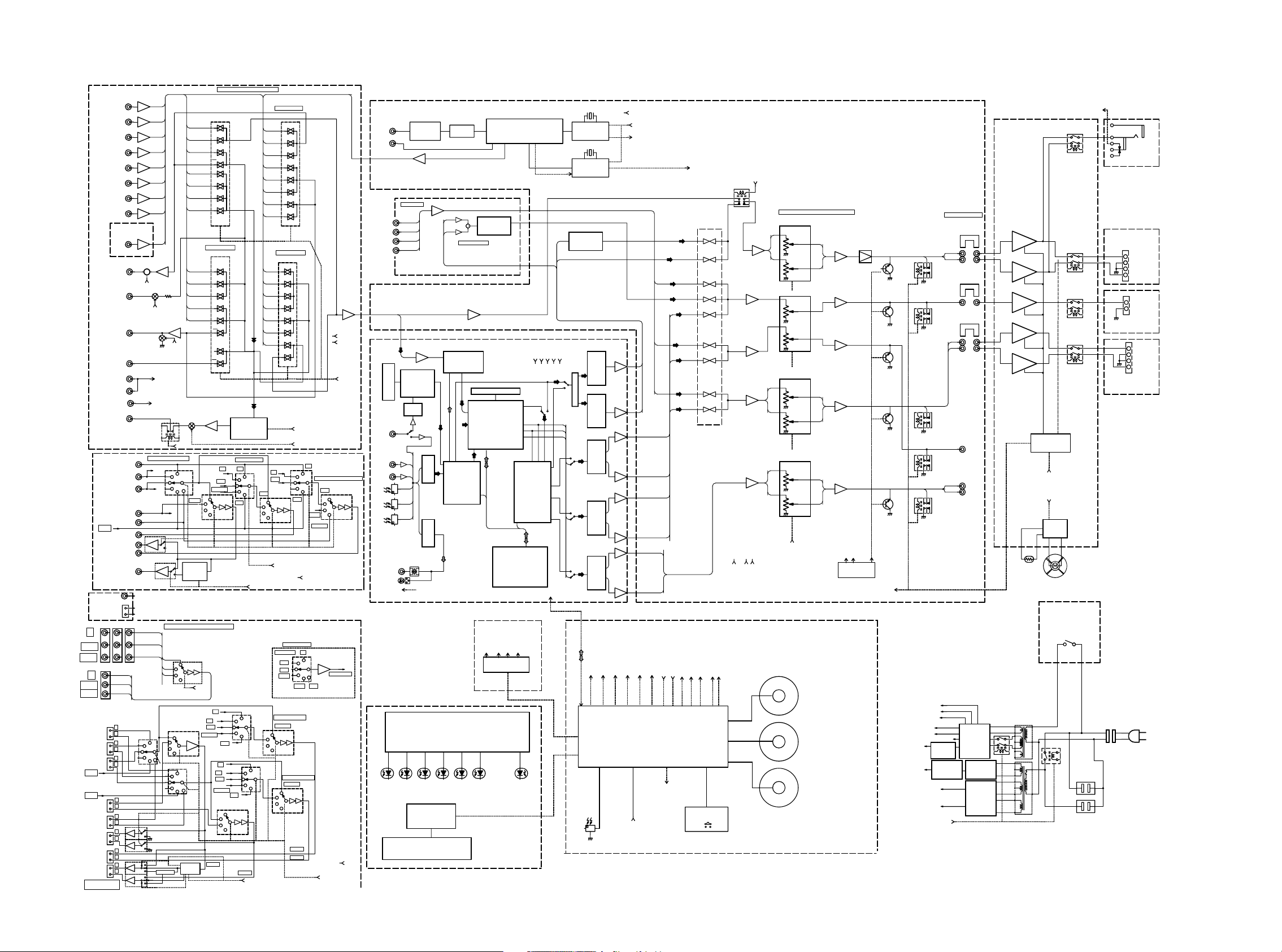
2. WIRING DIAGRAM ..................................................................................................................................... 3
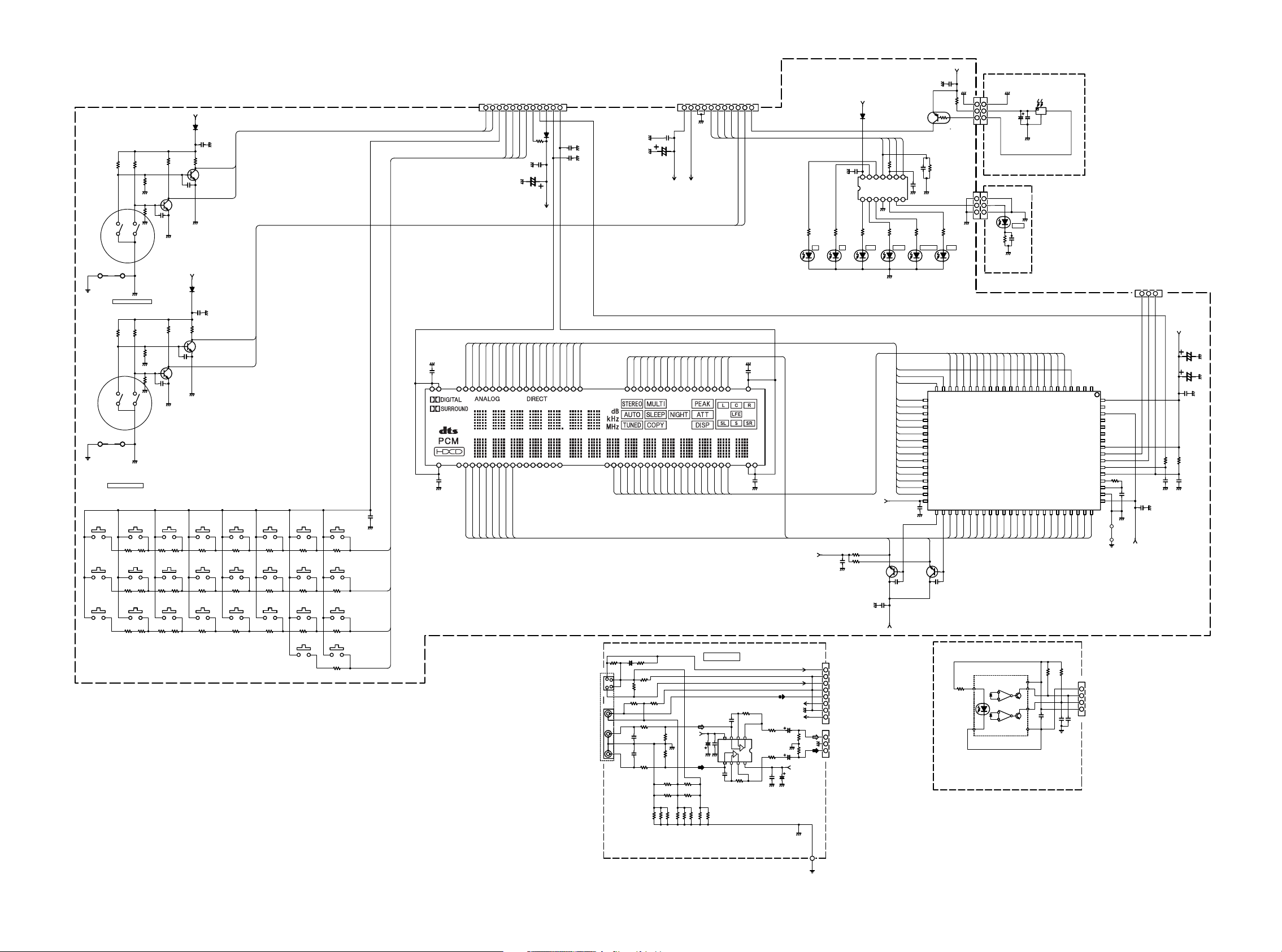
3. BLOCK DIAGRAM ....................................................................................................................................... 5
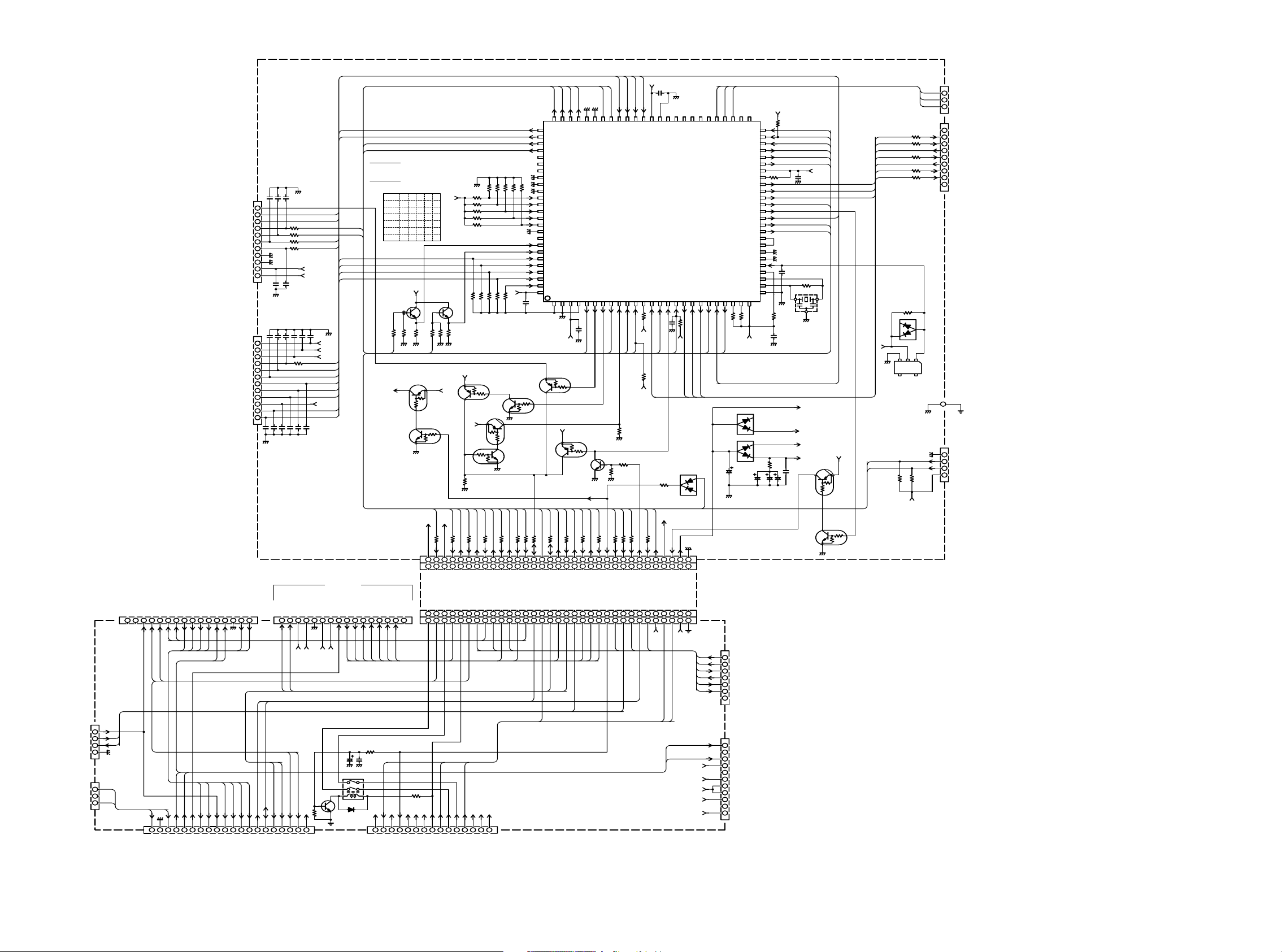
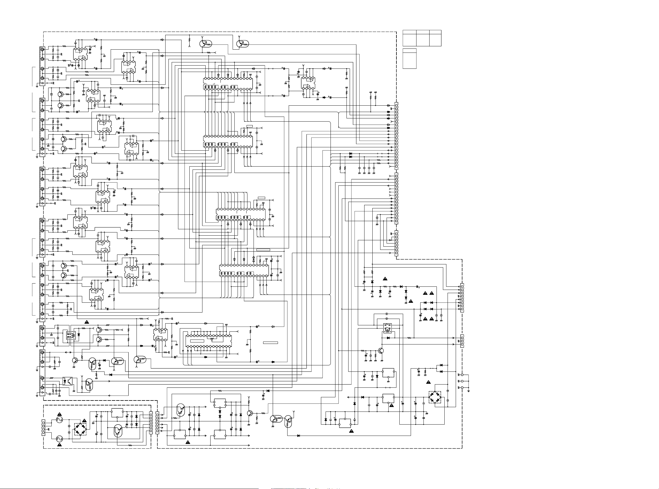
4. SCHEMATIC DIAGRAM .............................................................................................................................. 7
5. PARTS LOCATION (Pattern Side) ............................................................................................................ 31
6. IC DATA .................................................................................................................................................... 51
7. EXPLODED VIEW AND PARTS LIST ....................................................................................................... 61
8. SERVICE PROGRAM ............................................................................................................................... 67
9. ELECTRICAL ADJUSTMENTS ................................................................................................................. 69
10. ALIGNMENT PROCEDURES ................................................................................................................... 71
11. TROUBLE SHOOTING ............................................................................................................................. 73
12. TECHNICAL DESCRIPTION FOR DECODER ......................................................................................... 76
13. ELECTRICAL PARTS LIST ....................................................................................................................... 78
TABLE OF CONTENTS
AV Surround Receiver
SR-17EX/SR-18EX
SR-14EX/SR-14mkll
Please use this service manual with referring to the user guide ( D.F.U. ) without fail.
Printed in Japan
SR-14EX/SR-14mkII
SR-17EX/SR-18EX
R
326J855010 MIT
3120 785 22430
First Issue 2000.12
MARANTZ DESIGN AND SERVICE
MARANTZ AMERICA, INC.
Using superior design and selected high grade components, MARANTZ company has created the ultimate in stereo sound.
Only original MARANTZ parts can insure that your MARANTZ product will continue to perform to the specifications for which
it is famous.
Parts for your
MARANTZ equipment are generally available to our National Marantz Subsidiary or Agent.
ORDERING PARTS :
Parts can be ordered either by mail or by Fax.. In both cases, the correct part number has to be specified.
The following information must be supplied to eliminate delays in processing your order :
1. Complete address
2. Complete part numbers and quantities required
3. Description of parts
4. Model number for which part is required
5. Way of shipment
6. Signature : any order form or Fax. must be signed, otherwise such part order will be considered as null and void.
USA
MARANTZ AMERICA, INC
440 MEDINAH ROAD
ROSELLE, ILLINOIS 60172
USA
PHONE : 630 - 307 - 3100
FAX : 630 - 307 - 2687
AMERICAS
SUPERSCOPE TECHNOLOGIES, INC.
MARANTZ PROFESSIONAL PRODUCTS
2640 WHITE OAK CIRCLE, SUITE A
AURORA, ILLINOIS 60504 USA
PHONE : 630 - 820 - 4800
FAX : 630 - 820 - 8103
AUSTRALIA
QualiFi Pty Ltd,
24 LIONEL ROAD,
MT. WAVERLEY VIC 3149
AUSTRALIA
PHONE : +61 - (0)3 - 9543 - 1522
FAX : +61 - (0)3 - 9543 - 3677
NEW ZEALAND
WILDASH AUDIO SYSTEMS NZ
14 MALVERN ROAD MT ALBERT
AUCKLAND NEW ZEALAND
PHONE : +64 - 9 - 8451958
FAX : +64 - 9 - 8463554
EUROPE / TRADING
MARANTZ EUROPE B.V.
P.O.BOX 80002, BUILDING SFF2
5600 JB EINDHOVEN
THE NETHERLANDS
PHONE : +31 - 40 - 2732241
FAX : +31 - 40 - 2735578
AUSTRALIA
TECHNICAL AUDIO GROUP PTY, LTD
558 DARLING STREET,
BALMAIN, NSW 2041,
AUSTRALIA
PHONE : 61 - 2 - 9810 - 5300
FAX : 61 - 2 - 9810 - 5355
THAILAND
MRZ STANDARD CO.,LTD
746 - 754 MAHACHAI ROAD.,
WANGBURAPAPIROM, PHRANAKORN,
BANGKOK, 10200 THAILAND
PHONE : +66 - 2 - 222 9181
FAX : +66 - 2 - 224 6795
TAIWAN
PAI- YUING CO., LTD.
6 TH FL NO, 148 SUNG KIANG ROAD,
TAIPEI, 10429, TAIWAN R.O.C.
PHONE : +886 - 2 - 25221304
FAX : +886 - 2 - 25630415
BRAZIL
PHILIPS DA AMAZONIA IND. ELET. ITDA
CENTRO DE INFORMACOES AO
CEP 04698-970
SAO PAULO, SP, BRAZIL
PHONE : 0800 - 123123
FAX : +55 11 534. 8988
(Discagem Direta Gratuita)
CANADA
LENBROOK INDUSTRIES LIMITED
633 GRANITE COURT,
PICKERING, ONTARIO L1W 3K1
CANADA
PHONE : 905 - 831 - 6333
FAX : 905 - 831 - 6936
SINGAPORE
WO KEE HONG DISTRIBUTION PTE LTD
130 JOO SENG ROAD
#03-02 OLIVINE BUILDING
SINGAPORE 368357
PHONE : +65 858 5535 / +65 381 8621
FAX : +65 858 6078
MALAYSIA
WO KEE HONG ELECTRONICS SDN. BHD.
SUITE 8.1, LEVEL 8, MENARA GENESIS,
NO. 33, JALAN SULTAN ISMAIL,
50250 KUALA LUMPUR, MALAYSIA
PHONE : +60 3 - 2457677
FAX : +60 3 - 2458180
JAPAN
MARANTZ JAPAN, INC.
Technical
35- 1, 7- CHOME, SAGAMIONO
SAGAMIHARA - SHI, KANAGAWA
JAPAN 228-8505
PHONE : +81 42 748 1013
FAX : +81 42 741 9190
KOREA
MK ENTERPRISES LTD.
ROOM 604/605, ELECTRO-OFFICETEL, 16-58,
3GA, HANGANG-RO, YONGSAN-KU, SEOUL
KOREA
PHONE : +822 - 3232 - 155
FAX : +822 - 3232 - 154
SHOCK, FIRE HAZARD SERVICE TEST :
CAUTION : After servicing this appliance and prior to returning to customer, measure the resistance between either primary AC
cord connector pins ( with unit NOT connected to AC mains and its Power switch ON ), and the face or Front Panel of product and
controls and chassis bottom.
Any resistance measurement less than 1 Megohms should cause unit to be repaired or corrected before AC power is applied, and
verified before it is return to the user/customer.
Ref. UL Standard No. 1492.
In case of difficulties, do not hesitate to contact the Technical
Department at above mentioned address.
001120MIT

1. TECHNICAL SPECIFICATIONS
FM TUNER SECTION
Frequency Range ......... 87.5 − 108.0 MHz (K, N, S, U version)
76.0 − 90.0 MHz (F version)
Usable Sensitivity ............................................ IHF 1.8 µV / 16.4 dBf
Signal to Noise Ratio ......................... Mono / Stereo 76 / 72 dB
Distortion ............................................Mono / Stereo 0.2 / 0.3 %
Stereo Separation ................................................... 1 kHz 45 dB
Alternate Channel Selectivity .... ±400 kHz 60 dB (F, U version)
±300 kHz 60 dB (K, N, S version)
Image Rejection ................................................... 98 MHz 70 dB
Tuner Output Level .. 1 kHz, 75 kHz Dev 800 mV (F, U version)
1 kHz, 40 kHz Dev 800 mV (K, N, S version)
AM/LW TUNER SECTION
Frequency Range ......... AM(MW) : 520 − 1710 kHz (U version)
531 − 1602 or 520 − 1710 kHz (K version)
531 − 1602 kHz (F, N, S version)
LW : 152 − 282 kHz (N version)
Signal to Noise Ratio ......................................................... 50 dB
Usable Sensitivity ................................................... Loop 400 µV
Distortion ............................................400 Hz, 30 % Mod. 0.5 %
Selectivity ......................................... ±20 kHz 70 dB (U version)
±18 kHz 70 dB (K, N, S version)
AUDIO SECTION
Rated Power
FRONT (20 Hz − 20 kHz) .......................... 8 ohms 140W / Ch
Center (20 Hz − 20 kHz) ............................ 8 ohms 140W / Ch
Surround (20 Hz − 20 kHz) ....................... 8 ohms 140W / Ch
THD Front (20 Hz − 20 kHz) ................................ 8 ohms 0.05%
Input Sensitivity / Impedance
Linear ....................................................... 350 mV / 47 kohms
Signal to Noise Rate ( IHF A )
Linear ............................................................................ 106 dB
Frequency Response
(Analog Input / Source Direct) .............. 8 Hz - 80 kHz (±3 dB)
(Digital Input / 96 kHz PCM) ................. 8 Hz - 45 kHz (±3 dB)
Dolby Digital(AC-3) SECTION
Output Level ( Master Volume is set 0dB )
Front L / R, CENTER, SURROUND L/R
1 kHz, 20 dB FS INPUT.................................................. 0.24V
SUBWOOFER
40 Hz, 0 dB FS INPUT ..................................................... 7.5V
Frequency Response
Front L / R, CENTER, SURROUND L / R ( LARGE )
20 Hz − 20 kHz ............................................................. -0.5 dB
Total Harmonic Distortion
Front L / R, CENTER, SURROUND L / R and
SBL / SB (1 kHz ) .................................................. 0.01% or less
SUBWOOFER ( 40 Hz) ........................................ 0.07% or less
Signal to Noise Ratio ( IHF-A ) .......................................... 80 dB
Channel Separation ( 1 kHz ) ........................................... 95 dB
Specifications subject to change without prior notice.
VIDEO
Television Format ...................................... NTSC (F, U version)
PAL/NTSC (K, N, S version)
Input Level / Impedance ................................ 1 Vp-p / 75 ohms
Output Level / Impedance ............................. 1 Vp-p / 75 ohms
Video Frequency Response .................. 5 Hz to 8 MHz ( - 1 dB)
S/N ..................................................................................... 60 dB
GENERAL
Power Requirement ........................ AC 120V 60 Hz (U version)
AC 220V 50 / 60 Hz (K version)
AC 100V 50 / 60 Hz (F version)
AC 230V 50 Hz (N, S version)
Power Consumption .......................................................... 530W
Dimension ( MAX )
Width ........................................................ 18 inches (458 mm)
Height .................................................... 7-½ inches (190 mm)
Depth ................................................... 19-½ inches (496 mm)
Weight (SR14A ) ......................................... 58.4 lds. (26.5 kg)
Weight (SR17A ) ......................................... 56.4 lds. (25.2 kg)
Weight (SR18A ) ......................................... 53.9 lds. (24.5 kg)
ACCESSORIES
Remote Control Unit
RC5000i (SR14A) ...................................................................1
RC-18SR (SR18A / SR17) ..................................................... 1
1
Remark : Bass signal output fr om Sub Woofer terminal for SR-14EX/SR-14mkII/SR-17EX/SR18-EX.
Sub woofer output is not active while all surround modes. Please refer to the following table.
SPK SETUP for SR-14EX/SR-14mkII/SR-17EX/SR18-EX
SPK setup
Sub Surr. Surr.B Bass CFG AUTO (PCM,Ana)
Woofer Front Center L/R (L/R) # THX Surr EX Stereo AUTO(AC-3,DTS) (AC-3:2ch,karaoke)
ON Large Large Large Large 1 LFE LFE none L+R LFE L+R 1
Small Large 3 LFE+SL+SR LFE+SL+SR none L+R LFE+SL+SR L+R 2
None (prohibit) 1 LFE LFE none L+R LFE L+R 3
Small Large Large 5 LFE+C LFE+C C L+R LFE+C L+R 4
Small Large 8 LFE+C+SL+SR LFE+C+SL+SR C L+R L FE+C+SL +SR L+R 5
None (prohibit) 5 LFE+C LFE+C C L+R LFE+C L+R 6
None Large Large 1 LFE LFE none L+R LFE L+R 7
Small Large 3 LFE+SL+SR LFE+SL+SR none L+R LFE+SL+SR L+R 8
Small Large Large Large 12 LFE+L+R LFE+L+R L+R L+R LFE+L+R L+R 10
OFF No output to subW
None (prohibit) 1 LFE LFE none L+R LFE L+R 9
Small Large 11 LFE+L+R+SL+SR LFE+L+R+SL+SR L+R L+R LFE+L+R+SL+SR L+R 11
None (prohibit) 12 LFE+L+R LFE+L+R L+R L+R LFE+L+R L+R 12
Small Large Large 10 LFE+L+R+C LFE+L+R+C L+R+C L+R LFE+L+R+C L+R 13
Small Large 0 LFE+L+R+C+SL+SR
None (prohibit) 10 LFE+L+R+C LFE+L+R+C L+R+C L+R LFE+L+R+C L+R 15
None Large Large 12 LFE+L+R LFE+L+R L+R L+R LFE+L+R L+R 16
Small Large 11 LFE+SL+SR LFE+SL+SR L+R L+R LFE+SL+SR L+R 17
None (prohibit) 12 LFE+L+R LFE+L+R L+R L+R LFE+L+R L+R 18
ZR38601
Small 14 LFE+Sb LFE
Small 16 LFE+SL+SR+Sb LFE+SL+SR
Small 18 LFE+C+Sb LFE+C
Small 21 LFE+C+SL+SR+Sb LFE+C+SL+SR
Small 14 LFE+Sb LFE
Small 16 LFE+SL+SR+Sb LFE+SL+SR
Small 25 LFE+L+R+Sb LFE+L+R
Small 24 LFE+L+R+SL+SR+Sb LFE+L+R+SL+SR
Small 23 LFE+L+R+C+Sb
Small 13
Small 25 LFE+L+R+Sb
Small 24 LFE+SL+SR+Sb
LFE+L+R+C+SL+SR+Sb
THX5.1, Dolby-D,
DTS
LFE+L+R+C+SL+SR L+R+C L+R LFE+L+R+C+SL+SR L+R 14
SubWoofer Output by Surround mode
THX4.0, Pro
Logic
NOTES
No.
2
2. WIRING DIAGRAM
FL(F)
J805
WHT/BLU
RED/BRN
W801
FL(F)
AC20V(24V)
AC9.7V(5V)
AC9.7V(5V)
AC20V(24V)
VH 8P EH 3P
1
2
3
4
5
6
7
8
L002
SUB-TRANS
21
WHT/BLU
RED/BRN
WB03
3
+24V
2
PH 3P
1
TEMP OUT
JB12
/JB62
WHT/BLU
JB05 JB09
B3P VH
/JB55 /JB59
POWER_SW
PB74
EH 6P
+24V
+12V
SUPPLY
P804
WHT/BLU
RED/BRN
L001
EH 6P
+24V
+12V
+24V
RELAY
J804
32187654321
WB02
BLU
BLU
YEL
BLK
YEL
ORG
GRY
ORG
JB04JB08
EH 3PB3P VH
/JB54/JB58
321
+24V
3
2
JB06/JB56
1
PRIMARY
PB04/
PB54
RED/BRN
2121
B3P VH
WB01
B3P VH
21
JB71
654321
J802
-24V
+15VA
J801
4321
VH 4P
MAIN-TRANS
-24V
+15VA
WY04
654321
J803
REF
AUDIO_FUNCTION
JY67
11
10
9
8
7
6
PH 11P
5
4
3
2
1
JY68
4
3
2
1
W753
JY69
3
2
EH 3P PH 4P
1
WL71
JY07
1
2
3
PH 3P
JY02
WY02
YEL
1
GRY
2
GRN
3
RED
1
BLK
2
ORG
3
SUPPLY
PS04
AUX-L
L OUT(LT)
GND(NC)
R OUT(RT)
-15VD
GND(NC)
+15VD
+5VAD
+5VAD
-5VD
GND(NC)
+3.3V
RELAY CTRL
H.P.SW
MUTE- RELAY
AUX-R
GND(NC)
AUX-L
FL
FL
FLDATA
FLCLK
FLRST
GND(NC)
R OUT
L OUT
AUX-R
FL
CE0(ANA.SW)
CE7(P.EXP)
FL
DSP-DI
DSP-DO
DSP-CLK
PH 9P
-24V
TUNER-R
TUNER-L
987654321
987654321
JY64
+24V
CE3(TONE)
RDS-DI
PY54
+24V
µ
-COM
PY04
DSP-ACK
DSP-RST
DSP-REQ
MULTI-MUTE
RELAY-MUTE
VCR1-MUTE
CDR/MD-MUTE
13
12
11
10
20P
13
12
11
10
CE6(P.EXP)
CE1(OSD)
TU-SD
987654321
987654321
987654321
987654321
GND(NC)
DSP-MUT
987654321
DATA0
RC-5
MULTI-RC
TAPE-MUTE
16
15
14
15
14
CE2(OSD)
TU-DI
JY05
WU91
J806
+15VD
CE3
CE0
CLK0
JS09
20201919181817
1716
CONNECT
PY64
LRG/SML
P-DOWN
SYNC DET2
DATA0
RC-5
33P
33P
+5VL
DN
UP
2
1
3
PH 4P
PH 4P
JU91
GYRO
ENCODER
PU94
EH 7P
+8V
+8V
+5A.D(+5VD1)
-5VD
-15VD
POWER
MULTI-RC-OUT
123456789
H.P.SW
SYNC DET1
OSD-2
OSD-1
CLK0
+5VA
+5VB
+5VC
+5VD
FL
4
2
1
4321
+5VD +5VD
+5VV
+5VL
POWER
FL
-15VA
+5VD
3
7654321
+12V
+3.3V
+15VA
+24V
987654321
15P
JY65
RELAY CTRL
TU-CE
4
PH 12P
W756
FL(F)
FL(F)
VKK
+3.3V
P-DOWN
13
12
11
10
13
12
11
10
RELAY-MUTE(M-RL)
+15VA
MULTI-RC
TU-DO
TU-CLK
+15VA
JY03
98765
+5AD
+5VV
JS10
15
14
15
14
CE3(TONE)
CE0(ANA.SW)
LRG/SML
CE6(P.EXP)
CDR/MD-MUTE
MULTI-MUTE
VCR1-MUTE
TAPE-MUTE
TUNER-R
TUNER-L
DATA0
+15VA
-15VA
+5VL
+5VV
-24V
SYNC DET1
SYNC DET2
CE1(OSD)
CE2(OSD)
CE7(P.EXP)
OSD-INT
VKK
+5VL
MULTI-RC-OUT
VKK
+5VL
+5VB
1211
10
JY63
N.C
N.C
R OUT
L OUT
JY62
CLK0
OSD-1
OSD-2
JY70
GND(NC)
333231302928272625242322212019181716151413121110
333231302928272625242322212019181716151413121110
JY51
JY53
333231302928272625242322212019181716151413121110
333231302928272625242322212019181716151413121110
VKK
+5VL
CLK0
DATA0
VOL_DN
VOL_UP
JY61
JY01
CLR
CE5
IR
JY04
16
15
14
13
12
11
10
9
8
PH 16PPH 16P
7
6
5
4
3
2
1
16
15
14
13
12
11
10
9
8
7
6
5
4
3
2
1
7
6
5
4
3
2
1
WY51
WY05
11
10
9
8
7
6
5
4
3
2
1
JL77
321
EH 3P
WY62
WL02
WY61
PH 7P
PH 11P
WY01
AUX_INPUT
PL74
JZ06
PL04
S-VIDEO_FUNCTION
COMPONENT_VIDEO
C
JZ08
IR_SENSOR
PU84
321
XH 3P
321
11
VKK
10
+5VL
+5VIR
9
8
FRONT_DISPLAY
7
6
PH 11P
5
4
3
2
FL(F)
1
JU01
21
WY03
JL76
WZ01
1
2
3
4
5
PH 8P
6
-15VA
7
8
+15VA
PH 16P
7654321
Y
GND(NC)
JU81
JU03
RCIR
FL(F)
+5VD
98
+5VV
-24V(NC)
-15VA
AUX-CVBS
GND(NC)
+5VIR+5VL
PU04
KEY1
DI-FL
STB
PH 12P
+5VL
GND(NC)
-15VA
+15VA
GND(NC)
87654321
STANDBY
LED
PU74
XH 3PXH 3P
XH 3P
KEY4
KEY3
KEY2
98
76543
151413121110
+15VA
+5VB
JZ07
JU71
321
321
JU04
LED-CONT
JU05
RIGHT
LEFT
121110
JU02
M06-CONNECT
PH 16P
WY63
16
15
14
13
12
11
10
9
8
PH 16P
7
6
5
4
3
2
1
16
15
14
13
12
11
10
9
8
PH 16P
7
6
5
4
3
2
1
4(B) 5 3 2 1
INP.SEL
JL09
B A
COPY
(B) (A) C
VIDEO MUTE
DSS:L/DVD:H
PAL
GND(NC)
AUX-CVBS
987654321
JL10
-24V
+5VV
PZ04
CVBS_FUNCTION
6CH_IN
+5VL
GND(NC)
-15VA
+15VA
16151413121110
WL01
16
JC71
16151413121110
PH 16P
987654321
15
14
13
12
11
10
9
8
PH 16P
7
6
5
4
3
2
1
KILLCON
SL6
GND
SR6
C6
GND
SW6
FR
GND
FL
SWA
VCLK
VDATA
OSD-OUT
CLK0
DATA0
JC03
PH 16P PH 16P
JC04
+5VL
+5VV
+15VA
-15VA
-24V(NC)
P104
M02-6CH IN
TO JL07 (PL04)
TU-CLK
PH 7PPH 8P
TU-CE
RDS-DO
11
10
9
8
7
PH 11P
6
5
4
3
2
1
PLL-DO
TU-SD
7654321
J602
J105
GNDA
-15VD
GNDA
+15VD
+5VAD
+5VAD
-5VD
GNDD
+3.3V
WL03
JM04
N.C
TU-DI
87654321
TUNER
ELE_VR
ERMUTE
-15VA
+15VA
+5VA
+5VD
987654321987654321
JC01
TUNER GND ONLY
FRFLC
PH 14PPH 8P
PH 14P
DSP
P604
PH 9P
1615141312111016151413121110
FR OUT
FR IN
+15VA
-15VA
FL OUT
+15VAM+15VA
FL IN
JC02
SW
RS
LS
1413121110
987654321
JM22JM21
JC08JC07
5
4
3
5P5P
2
1
PW04
5
4
3
NC
2
NC
1
HDAM
W601
1413121110
987654321
J601
J691
987654321
WT01
EH 7P
J871
JW02
VH 3P
W701
TEMP.SENS
S701
4
3
2
1
W751
WN51
PH 3P
MN51
12V FAN
W851
EH 4P
W754
321
J703
VH 3P
EH 3P
W703
4
L
+8V
+8V
3
2
R
EH 4PVH 4P
1
AUTO MODE
+5A.D(+5VD1)
JN08
FR/LS_POWER_AMP
4
-B
3
+B
PROTECTOR
2
1
PO-DWN
JN02
JN09
3
STOP
2
PH 3P
1
DC-IN
JN04
W755
J704
3
2
1
J715
3
2
1
NC
+B
+24V
J716
WY06
FLDATA
1
2
FLCLK
3
FLRST
PH 3P
VH 5P VH 4P
J853
POWER-AMP-SUPPLY
3
AC62V
2
VH 3P
1
AC62V
J851
54321
J852
P854
HEAD_PHONE
PW04
4321
3
-B -B
+B
-B
2
+B
1
J854
PH 3P
7654321
321
FR
LS
+3.3V
+12V
GND(NC)
JN03
FR
LS
RELAY
+B
JN05
54321
+5VV
P754
EH 5P
CENTER_SPK
PT74
EH 5P
54321
3MIX
C.DET
L.OUT
POSIST
J709
J785
FL/RS/C_POWER_AMP
J708
3CH_POWER_TR
JP01
4
3
2
1
6
5
4
3
2
1
+B
+B
W752
VH 6P PH 4P
JN72
P704
J707
J783
P774
WT51
C
3
B3P VH
VH 6P
6
5
JN53
4
3
2
1
JN56
-B
VH 5P
SPK_TERMINAL
PT04
+B
C
B3P VH
-B
J706
J782J784
JN51
32211
VH 7P
VH 7P
J702
C
J705
6
12345123451234565432154321
61234561234512345 12345 12345
J781
54321
JN52
7
654321
WT02
7
654321
RS
FL
1
2
3
PH 5P
4
5
J701
J717
1212
W702
TEMP.SENS
S702
3 4
3. BLOCK DIAGRAM
TAPE IN
CDR IN
VCR1 IN
DSS/VCR2 IN
TAPE OUT
CDR OUT
VCR1 OUT
DSS/VCR2
RC-5 IN
RC-5 OUT
MULTI ROOM
MULTI ROOM
COMPOSITE
DSS/VCR2
AUX
VCR1 OUT
DSS/VCR2 OUT
MULTI OUT
COMPOSITE
MONITOR OUT
COMPOSITE
PL94
AUX IN
Y
B-Y
R-Y
Y
B-Y
R-Y
MONITOR OUT
TV
LD
DVD
AUX
AUX
VCR1 IN
DSS/VCR2
IN
DSS/VCR2
OUT
VCR1
OUT
MONITOR
OUT
S-VIDEO
CD
TV
LD
DVD
AUX
OUT
RC-IN
OUT
VCR1
S
Y
C
Y
C
Y
C
Y
C
Y
C
Y
C
Y
C
Y
C
PL74
TV
LD
DVD
Y
B-Y
R-Y
MM1140XF
‚V‚Tƒ
‚V‚Tƒ
NJU2244D
‚V‚Tƒ
‚V‚Tƒ
NUM2263D
PS04
QS01
QS02
QS51
QS52
QS53
QS91
MUTE
CONTROL
RC-5 IN/OUT
VIDEO SELECTOR
NJM2244D
QL08
B-Y_X3
R-Y_X3
QZ01
QZ10
QZ09
TAPE
CDR
DVD
VCR1
DSS
AUX
MUTE
MM1140XF
Baf
NJM2244D
Y_X3
QZ19
NJU2244D
QZ20
NUM2263D
Y-C SEP.
CD
21
TU
(10)
22
CD
(9)
24
TAPE
TV
LD
(7)
25
(6)
27
TU
(4)
28
CD
(3)
29
TAPE
(2)
30
CDR
(1)
(30)
CDR
1
(29)
TV
2
(28)
DSS
3
(26)
DVD
5
(25)
VCR1
6
(24)
7
22
MUTE
MUTE
RELAY
QL01
LC74781
QZ02
BA7612N
LC74781
7
(1)
VCR1
BA7612N
OSD
BA7613N_X3
6dB
75OHM
CONTROL
DSS/V2
6dB
QZ03
OSD
QZ11
(9)
21
CONTROL
QL14
Baf
COMPONENT VIDEO SELECTOR
MM1140XF
INPUT SEL./MULTI SEL.
QS12
LC78211
(S1)
(11)
TP
(8)
26
(5)
INPUT SEL.
LC78212
QS14
(S2)
CDR
(27)
TV
DS
DV
(23)
V1
8
V1
20
V2
(11)
V2
(10)
5
(3)
QG02
LD
DVD
DSS/V2
+6dB
75OHM
QL02
QL09
TV
LD
DVD
AUX
TV
LD
DVD
DSS/V2
AUX
QZ04
BA7612N
OFF
Y-OUT
20
23
4
5
(24)
QG01
ELE. VOL
TC9459N
COPY SWITCH
BA7649A BA7649A
TV
QL05
SRC
AUX
OSD CONTROL
BA7649A
QZ05
BA7649A
QZ06
+6dB
‚V‚Tƒ
C-OUT
OSD CONTROL
COPY SWITCH
LC78212
QS13
(S4)
(30)
CDR
1
(29)
(27)
CD
TU
TV
LD
DVD
DSS
AUX
TV
LD
DVD
AUX
VCR1
DSS
AUX
2
(28)
3
(26)
5
(25)
6
(24)
7
(22)
9
(21)
10
MULTI ROOM
LC78211
30
(1)
29
(2)
28
(3)
27
(4)
25
(6)
24
(7)
22
(9)
21
AT
(10)
LD
DVD
QL06
+6dB
75OHM
BA7613N
FUNCTION
CONTROL
4
(23)
8
(20)
11
QS15
(S3)
26
(5)
23
(8)
20
(11)
MULTI VOL. CONTROL
MULTI MUTE
QL03
TV
AUX
VCR1
+5V
DSS/V2
PZ04
S2 DETECTOR
TV
CROMA-IN
DSS
DVD
VCR1
QZ22
VCR2 AUX
74HC4051
S-VIDEO BLOCK
COPY SWITCH
SOURCE
+6dB
QZ05
75OHM
BA7613N
COPY SWITCH
SOURCE
+6dB
‚V‚Tƒ
BA7612N
QZ07
Y-OUT
C-OUT
QS13
(5) (7)
+15V
-15V
FUNCTION
CONTROL
MULTI ROOM SELECTOR
QL04
BA7613N
OFF
+6dB
75OHM
PL04
VIDEO
QZ23
COMPARATER
CROMA-OUT
NJM2903D
+5V
FUNCTION
CONTROL
TUNER
P104 TUNER
FM
A101
FM FRONT
END
IF AMP
AM
DIRECT IN
CNT
SWF
SL
SR
PL04
13
QE09
PM4007
RF DEMOD.
256K-SRAM
2.88M
BPF
RF/
COAX
COAX
COAX
OPT
OPT
74HC15174HC151
QR01
LC89055
32K,44.1K
48K,96K
OPT
DIG.OUT
COAX
OPT
MUTE CONTROL
8BIT
P604
PORT EXPANDER
NJU3711L
FOR LED DRIVE
TV LD DVD VCR1 DSS AUX STANDBY
PU04
ML9205
FL DRIVER
FRONT
FL DISPLAY
VU01
+
Analog Lt/Rt
QK01
ADC
AK5392
FS=48K
DIR
YSS912C
FOR DOLBY DIGITAL
Q201
LA1837
FM/AM IF & MPX
80HZ-LPF
4TH-ORDER
P604 DSP
1M-SRAM
Q601
DTS
PRO LOGIC
PSEDOU
SURROUND
Q651
ZR38601
THX EX
(DELAY)
(BASS MANAGE)
(SPK CONFIG)
(PEAK LIMIT)
Q691
µ
-COM
16BIT
TMP93CW44ADF
FOR DSP CONTROL
(2LINES)
PAL/NTSC
DSS/DVD
FUNCT.CTL
FOR VIDEO
VIDEO MUTE
20BIT PORT
EXPANDER
PL04
PORT EXPANDER CONTROL
+15V
LT/RT
FOR
(16LINES)
CLOCK
KILLER
-15V
FM DET.
+5V
-5V
LC72130
RDS DECODE
(N, S ONLY)
80HZ-HPF
2ND-ORDER
D-SW
+3.3V
QD43
L/R
GATE ARRAY
C/SW
SL/SR
SBL/SBR
SUB CPU I/F
IR SENSOR
PLL
LC72722
Q351
QD01
DAC
AD1852
L
24BIT
96K
QD41
DAC
R
AD1852
24BIT
96K
QD03
C
DAC
AD1852
24BIT
96K
SW
QD02
SL
DAC
AD1852
24BIT
96K
SR
QD42
SBL
DAC
AD1852
24BIT
SBR
96K
OSD CONTROL
FUNCTION CONTROL
OSD CONTROL
16BIT µ-COM
TMP93CW40DF
FOR FEATURES
STEREO CONTROL
(FROM H.P.JACK)
+15V
PLL/RDS CONTROL
TUNING CONTROL
D-L
D-R
D-SBL
D-SBR
6CH DIRECT CONTROL
QY01
6CH-SL/SR
D-C
D-SW
D-SL
D-SR
POWER
P104
RDS DATA
LC78213
HPF-ON
HPF-OFF
6CH-SW
A-SW
D-SW
6CH-C
D-C
D-SL/SR
SPK RELAY CONTROL
PLL/RDS CONTROL
VOL CONTROL
KEY MATRIX
MULTI RC-IN
RC-5 IN/OUT
DIG/ANA
+15V
-15V
+5V
ROTARY ENCODER
ROTARY ENCODER
INDIVIDUAL & MASTER VOLUME
L/R
L
TC9459
R
C/SW
TC9459
SURR. L/R
SL
SR
SURR. BACK L/R
SBL
SBR
SL
TC9459
SR
SBL
TC9459
SBR
VOL CONTROL
PY04
µ
MAIN
MASTER VOLUME
GYRO CONTROL
FUNCTION
SELECT
L
R
-COM
HDAM
MLT-RC-MUT
DIG/ANA
12BIT PORT
EXPANDER
FRONT
MUTE CONTROL
MULTI RELAY
U-COM(+6V)
MUTE DRIVE
+5V(DIGITAL)
+5V(VIDEO)
+3.3V
+-15V(ANALOG)
SURR.AMP
+12V(FAN CONTROL)
STAND-BY CONTROL
24V,-33V
-5V
FL
PREOUT/MAININ
FRONT
L/R
CENTER
SURR. L/R
SUB WOOFER
SURR. BACK
L/R
POWER
+-8V
SUPPLY
POWER
SUPPLY
PS04
P754
POWER
SUPPLY
PS04
POWER
SUPPLY
P854
POWER
SUPPLY
P804
P704/P754
MAIN AMP
+29.0dB
MAIN
AMP
MAIN
AMP
MAIN
AMP
MAIN
AMP
MAIN
AMP
RELAY CONTROL
THERMOSENSOR
SUB
TRANSF.
PROTECTOR
DRIVE
SPEAKER RELAY
FAN CONTROL
COOLING FAN
PU94
POWER-SW
TRANSF.MAIN AMP
STEREO CONTROL
CONTROL
+12V
MAINS OUTLET
HEADPHONE
PT04
PT74
SURROUND
PT04
MAINS INLET
MAINS
PW04
FRONT
L
G
G
R
CENTER
G
L
G
G
R
5 6
4. SCHEMATIC DIAGRAM
+5.6VL
DU07
*
CU21
0.1/50V
RU61
RU62
RU57
10K
LEFT
WU01
INPUT SELECTOR
RU58
10K
RU60
DUMMY
RIGHT
RU59
DUMMY
CU08
100P
SU33
INPUT SELECTOR
10K
QU06
2SC536
SP/ETC
DU08
CU07
100P
+5.6VL
*
2SC536
SP/ETC
CU22
0.1/50V
10K
QU05
RIGHT
+5.6VL
CU24
DATA0
CU11
0.1/50V
CU13
1000P
HC10128090
DSS/V2
DU04 DU06
LT3K44B/GRN LT3K44B/GRN
0.1/50V
RU48
100
QU07
DTA114TS/ETC
RU44
100K
AUX
JU03
JU04
PU84
1
1
2
2
3
3
1
1
2
2
3
3
HLMF-K2
PU74
STANDBY
JU81
DU71
RED
RU71
680
IR SENSOR
HW10005020
CU82
220/6.3V
STBY
CU71
0.1/50V
QU81
CU81
22000PF
JU05
FLDATA
FLCLK
RST FL
1
23
INP-LT
INP-RT
+5VB
101112
JU02
RIGHT
LEFT
LEFT
PU04
Front
(RLE)
P.C Board
KEY3
KEY3
KEY2
STB(FL)
+5.6VD
FIL-A
FIL-B
KEY0
KEY1
DO
1
23456789
DU20
*
CU28
DUMMY
RU43
10K
KEY2
KEY1
KEY0
CU30
100/6.3V
CU27
0.01
CU29
DUMMY
+5VD
10/50V
CU31
CU32
0.01
JU01
VKK
+5.6VL
VKK
GND
10
11
+5.6VL
VOL-DOWN
VOL-UP
DATA0
CLK0
CE5
CLR
GND
CLR
R.C
1
23456789
CE5
CLK0
DATA0
DOWN
UP
RU32 RU33 RU34 RU35 RU36 RU37
180 180 180 180 180 180
TV
DU01
LT3K44B/GRN LT3K44B/GRN
+5.6VL
DU21
*
CLR
CE5
CLK0
100
RU63
CU12
0.1/50V
QU02
NJU3711
DU05
9
10
11
13
14
12
P1
P2
VDD
CLK
STB
CLR
P3P4P5P6VSSP7P8 D ATA
12345678
DVD
VCR1LD
DU02
DU03
LT3K44B/GRN
LT3K44B/GRN
CU05
100P
QU04
2SC536
SP/ETC
RU55RU56
10K10K
QU03
2SC536
SP/ETC
DOWN
UP
RU51
10K
D0WN
RU52
10K
RU53
DUMMY
RU54
DUMMY
UP
MASTER VOLUME
CU06
100P
SU32
WU02
MASTER VOLUME
SU01
SU09
SU17
SU02 SU03 SU04 SU05 SU06
******
AUTO
BAND
*
A/D
*
DOLBY THX
RU01
RU02 RU03 RU04 RU05 RU06 RU07 RU08 RU09
6.8K
470
3.3K
330
SU10
RU11
6.8K
SU18 SU19
RU21
6.8K
SU11
**
FM MODE
RU12 RU13 RU14 RU15 RU16 RU17 RU18 RU19
470
3.3K
330
***** **
RU22 RU23 RU24 RU25 RU26 RU27 RU28 RU29
COPY
ATT
470
3.3K
330
EX DTS
2.2K
1.5K
SU12 SU13
**
2.2K
SU20
DIG
COPY VCR1 COPY TAPE
2.2K
PRESETCLEARMEMO
1.5K
SU21
1.5K
SU14 SU15
SU22 SU23 SU24
SU07 SU08
SURR.
1K
**
AUTO TUN
1K
820 680
S-DIR
1K
820 680
SU25 SU26
CU23
0.1/50V
5CH ST STEREO
**
820 680
SU16
*
TREB+
TREB- BASS-
RU31
680
DISP-OFF
MULTI
**
KEY0
BASS+
KEY1
KEY2
KEY3
CU25
0.1/50V
CU10
0.1/50V
51
S33
S34
S35
S36
4445
42434849
55 56 57 58 596061
54
G24
G23
G22
G21
S32
32333435363738394041
62 63 64 65 66 67 68 69 76 77 78 798081
S19
S20
2728293031
VU01
S21
S22
S23
S24
S25
S26
S27
S28
S29
S30
S31
HQ32401410
G17
G18
G19
G20
C
S-VIDEO
Y
VIDEO
L
AUX INPUT
R
JL75
S17
S18
CL83
10UF/16V
RL86
CL75
470P
CL76
470P
N,S ONLY
CL75,CL76
CL77,CL78
75
50V
50V
G16
20
S16
RL94
DUMMY
RL88
G15
S15
RL85
G9G8G7G6G5G4G3G2G1
G11
G10
G14
G13
G12
1213141516171819
82 83 84 85 86 87 88 899091
S10
S11
S12
S13
S14
75
CL84
0
1/4W
CL88
75
0
1/4W
RL75
RL76
1K
1K
RL77
47K
RL78
47K
RL90
DUMMY
RL91
DUMMY
-15VA
RL92
DUMMY
RL93
DUMMY
CL82
10/50V
92 93 94 97 98
S1S2S3S4S5S6S7S8S9
AUX IN
CL77
47P
CL90
0.1U
16V
CL78
47P
CU26
0.1/50V
+
-
RL80
0
0.1/50V
2567891011
PL74
RL79
0
+
CU09
QL75
NJM4558M
RL81
RL82
CL89
0.1U
0
10/50V
16V
(M07)
-15VA
+15VA
CL79
10/50V
CL80
0
CL81
10/50V
RL84
+15VA
RL83
47K
+5VD
CU04
100/6.3V
SEG5
COM16
G16
SEG4
COM17
RU92
DUMMY
SEG2
SEG3
COM18
COM19
G19
G18
G17
CU91
0.1
CU93 CU94
DUMMY DUMMY
S1S2S3S4S5S6S7S8S9
SEG1
COM20
G20
RU93
DUMMY
JU91
AD4
COM21
G21
AD2
AD3
HC10039260
COM22
COM23
G23
G22
1
2
3
4
AD1
COM24
GND
UP
DN
+5VD
1
80
VDISP2
NC
VFL2
P4
P3
P2
P1
VDD
DA
CP
CS
RESET
OSC1
OSC0
GND
VFL1
65
64
G24
RU42
3.3K
CU20
47P
CU03
0.1/50V
WU03
1P
WIRE
VKK
TO JY05 (PY04)
M07 MAIN U-CON PCB
CU17
1000P
RU41
CU33
DUMMY
CU01
0.1/50V
RU40
100
1K
CU14
0.1/50V
S10
S11
S12
S13
S14
S15
S16
S17
QU09
S18
24
SEG17
SEG18
SEG19
SEG20
25
SEG21
SEG22
SEG23
SEG24
SEG25
SEG26
SEG27
SEG28
SEG29
SEG30
SEG31
SEG32
SEG33
SEG34
SEG35
VDISP1
COM2
COM3
COM4
COM1
40
41
G3G4G5
G2
CU19
100P
SEG16
COM5
SEG15
COM6
G6
SEG14
COM7
G7
SEG13
COM8
SEG11
SEG12
QU01
ML9205-01GA
COM10
COM9
G10G9G8
SEG10
COM11
G11
SEG9
COM12
G12
SEG8
COM13
G13
SEG7
COM14
G14
SEG6
COM15
G15
S36
S19
S20
S21
S22
S23
S24
S25
S26
S27
S28
S29
S30
S31
S32
S33
S34
S35
+5VD
CU02
0.1/50V
QU08
2SC536
SP/ETC
CU15
0.1/50V
G1
2SC536
SP/ETC
CU18
100P
+5VD
RU38
CU16
0.1/50V
RU39
10K
10K
VKK
JL76
1
C
2
GND
3
Y
4
GND
5
AUX-CVBS
6
-15VA
7
GND
8
+15VA
AUX-L
1
2
GND
3
AUX-R
47K
JL77
*
M02 S-VIDEO
TO JZ08 (PZ04)
TO JY69 (PY64)
M06 CONNECT PCB
(RLF)
RU91
330
PU94
QU91
GP1A06
(M05)
GYRO ENCODER
1/4W01/4W01/4W01/4W01/4W01/4W01/4W01/4W
0
CL91
CL92
CL93
CL94
CL95
CL96
CL97
CL98
(RLD)
WL75
YB00152110
7 8
JY04
1
R.C
2
VOL-UP
3
VOL-DOWN
4
DATA0
5
CLK0
6
CE5
7
CLR
M05 FRONTM05 FRONT
TO JU01 (PU04)
+5.6VL
8
GND
9
GND
10
11
VKK
CY12
JY03
FIL-A
1
FIL-B
2
+5.6VD
3
STB(FL)
4
DO
5
KEY0
6
KEY1
7
KEY2
8
9
KEY3
TO JU02 (PU04)
TO JC01 (P104)
M03-TONE
JY63 JY62
CE3(TONE)
N.C
N.C
MUTE-RELAY
16 15 14 13 12 11 10
CE0(ANA.SW)
LRG/SML
CE6(P.EXP)
987654321
VCR-MUTE
TAPE-MUTE
MULTI-MUTE
CDR/MD-MUTE
R OUT
INP-LT
INP-RT
L OUT
+5VB
GND
10
11
12
TUNER-R
TUNER-L
DUMMY
DUMMY
DUMMY
CY16
CY15
CY14
RY56
RY55
RY54
RY53
16V0.1U
0.1U
CY13
50V1000P
16V0.1U
DUMMY
DUMMY
CY24
CY23
CY26
CY25
RY52
0
16V0.1U
DUMMY
DUMMY
DUMMY
CY20
CY18
CY17
CY19
DATA0
CLK0
16 15 14 13 12 11 10
+15VA
CE5
STB
VOL-UP
VOL-DN
0
0
0
0
+5VL
VKK
DATA0
CLK0
CE5
CLR
KEY1
KEY2
KEY3
KEY4
16V
DUMMY
DUMMY
CY28
CY27
FL-A
FL-B
+5VD
STB
DI-FL
KEY1
KEY2
KEY3
KEY4
+5VB
INP-LT
INP-RT
DUMMY
DUMMY
CY22
CY21
TO JC04 (P104) M03-TONE
TO JL10 (PL04) M02-VIDEO
TO JZ06 (PZ04) M02-S-VIDEO
COMMON BUS
-15VA
+15VA
-15VA
-24V
+5VL
SYNC DET1
+5VV
GND
987654321
+5VL
+5VV
MAIN µ-COM
PY04
CE1
CE2
SR-14EX
RY18,20=Y RY19,21=N
SR-18EX
RY18,20=N RY19,21=Y
RY14
RY15
RY16
RY17
RY22
RY23
+5VD
CE1(OSD)
OSD-2
OSD-1
SYNC DET2
N
N
QY11
2SC536
SP/ETC
5.2
47K
27K
RY57
RY64
+15VA
DTA114ES
NC
CE7(P.EXP)
CE2(OSD)
S
YYYYY
NN
+5VA
10K
RY58
QY10
/ETC
DTC114ES
(RLC)
UKF
N
N
N
YNN
Y
NYY
Y
N
NNN
Y
N
YYYYN
QY12
2SC536
4.8
SP/ETC
5.6
68K
RY59
+24V
QY09
/ETC
CE0
FL-A
0
RY32
FL
CE0(ANA.SW)
+5VA
27K
10K
RY68
RY60
+5VA
+5VL
CE7
+24V
FL-B
0
RY33
FL
CE7(P.EXP)
P.C Board
(M07)
Y=O OHM
RY15
RY14
RY16
RY18
RY20
RY22
Y=47K OHM
4.7K
4.7K
RY28
RY27
5.0
QY08
DTA114ES
/ETC
5.0
+5VA
0
RY04
47K
CE6
CE3
TU-SD
RDS-DI
0
220
RY34
RY35
987654321
987654321
+24V
RDS-DI
CE3(TONE)
CE6(P.EXP)
987654321
987654321
RY17
4.7K
4.7K
RY30
RY29
DTA114ES
5.0
DTC144ES
CE1
0
RY36
TU-SD
CE1(OSD)
RY21
RY19
+5VB
4.7K
RY31
CY10
0.01U
QY07
DTC114ES
/ETC
QY05
/ETC
QY04
/ETC
CE2
TU-DI
0
RY37
TU-DI
CE2(OSD)
80
RY23
90
100
50V
LRG/SML
220
220
RY38
RY65
LRG/SML
76
CE-LED
CE-FL
CE-OSD
CE-OSD2
NC
NC
NC
NC
NC
NC
SW0
SW1
SW2
SW3
SW4
VSS
S-STREG
POW-DET
ABNORMAAL
KEY0
KEY1
KEY2
KEY3
KEY4
VREFH
P-DOWN
RC-5
P-DOWN
CE6
75
1
0
+5VA
DATA0
220
RY39
DATA0
CE-MUTE
VREFL
CY11
0.1U
16V
0
S-DET2
CE0
CE7
CE3
CE-VOL
CE-VIDEO
CE-AUDIO
NMI
AVCC
AVSS
POWER
+5VC
QY06
DTA114ES
/ETC
0
QY03
DTA114ES
/ETC
QY02
2SC536
SP/ETC
CLK0
OSD-1
H.P.SW
220
220
RY41
RY40
CLK0
OSD-1
H.P.SW
SYNC DET2
+5VC
VOL-DN
VOL-UP
INP-RT
GYRO-DN
GYRO-A
VOL.ENC.B
INP-LT
VOL.ENC-A
FUC-ENC-A
FUNC-ENC-B
QY01
TMP93CW40DF
70
GYRO-UP
NC
NC
GYRO-B
16BIT µ-COM
N.C.(P83)
HEADPHONE
SYNC0
RC-5IN
SPKOFF
RC-5OUT
KILL-IR
POWER-OFF
5VC
RELAY
S-DET1
H.P.SW
10K
RY07
+5VA
RY05
47K
5.0
RY03
0
47K
RY02
18K
OSD-2
TU-CE
RELAY
S-DET1
220
RY42
POWER
OSD-2
SYNC DET1
TU-CLK
220
220
220
RY44
RY66
RY43
TU-CE
RELAY CTRL
TU-DO
220
RY45
TU-CLK
MULTI-RC
VCC
SURR-ACK
10K
RY06
S-DET2
DSP-ACK
RY46
+15VA
+15VA
TU-DO
+15VA
VSS
SYNC1
CY09
50V0.01U
60
NCNCNCNCNC
DO-0
P-DOWN
MULRTI-IN
0.1
CY69
+5VA
P-DOWN
DSP-DO
DY03
ISS301
0
VKK
333231302928272625242322212019181716151413121110
333231302928272625242322212019181716151413121110
VKK
+5VL
MULTI-RC-OUT
333231302928272625242322212019181716151413121110
333231302928272625242322212019181716151413121110
+5VL
DI-0
10K
RY08
DSP-DI
GND
DATA
NC
DO-1
CLK-0
2010
DATA0
DI-FL
DSP-CLK
POWER
JY01
JY53
PY54
JY51
JY61
CLK
RST
NC
RDS-DI
RST-FL
CLK-FL
DATA-FL
TUNE-SD
TUNE-DI
TUNE-DO
TUNE-CLK
TUNE-CE
N.C.(ALE)
_SURR-REQ
_SURR-RESET
SMUTE
_LARGE/SMALL
MULTI-OUT
CLR-LED
OSD-ON1
OSD-ON0
TEST2
TEST1
N.C.(P97)
N.C.(P96)
RESET
N.C.(EA)
N.C.(CLK)
N.C.(AM8)
CLK-1
DI-1
RY09
10K
+5VC
CLK0
CY02
47/10V
(M03 OR M05)
JY70
7
TU-SD
6
TU-DI
5
TU-CE
4
RDS-DI
3
TU-CLK
2
TU-DO
1
N.C
51
NC
VCC
VSS
VCC
CY30
5.5V
X2
X1
25
ISS300
DY02
ISS300
RY01
1F
PCB
DY01
47
+5VA
RY67
10K
50
RY13
10K
40
30
26
RY11RY10
10K10K
CY04
0.01U
50V
CY29
CY03
DUMMY
(RCO)
M03-TUNER
TO J105 (P104)TO J602 (P604)
CY07
1U
10V
CY01
0.1U
16V
DUMMY
RY12
+5VB
+5VL
+5VA
+5VC
RDS-DI
TU-CLK
TU-CE
CY08
LRG/SML
1M
0
TU-SD
TU-DI
TU-DO
+5VC
CLR
OSD-2
OSD-1
XY01
8MHZ
5.0
50V0.01U
QY13
DTC114ES
/ETC
DSP-REQ
DSP-RST
DSP-MUT
+5VA
QY14
/ETC
DTA114ES
0
+5VC
GYRO-UP
GYRO-DN
DSP-CLK
DSP-DO
DSP-DI
DSP-REQ
DSP-ACK
DSP-RST
DSP-MUT
RY24
4.7K
RY47
RY48
RY49
RY50
RY51
RY69
DUMMY
GND
VDD
NC
QY15
S-80730SN
+5VD
RY25
4.7K
JY07
DATA
3
DATA-FL
CLK
2
CLK-FL
RST
1
RST-FL
GND
1
DSP-CLK
2
0
3
DSP-DO
0
DSP-DI
4
DSP-REQ
5
0
DSP-ACK
6
DSP-RST
7
0
DSP-MUT
8
0
GND
9
M05 FRONT
TO JU05 (PU04)
M08-DSP
TO J691 (P604)
JY02
DY04
ISS300
OUTNC
JY06
*
JY05
GND
1
UP
2
DN
3
+5VD
4
TO JU91 (PU94)
M05 GYRO ENCODER
MUTE- RELAY
H.P.SW
RELAY CTRL
M01-AMP
TO JN03 (P754)
M07 AUX INPUT
TO JL77 (PL74)
AUX-L
GND
AUX-R
GND
JY68
1
2
3
4
JY69
*
1
2
3
987654321
GND
TO JS09 (PS04)
M04-AUDIO
AUX-L
AUX-R
L OUT
-24V
R OUT
TUNER-R
TUNER-L
VCR-MUTE
MUTE-RELAY
TAPE-MUTE
MULTI-MUTE
CDR/MD-MUTE
RC-5
MULTI-RC
CLK0
DATA0
QY61
+15VD
2019181716151413121110
+15VD
CE3(TONE)
CE0(ANA.SW)
LY61
24V
2SC3419
RY63
10K
JY64
CY62
10/50V
DY61
1D3
CY61
RY62
10K
0.01
-15VD
-5VD
-5VD
-15VD
MULTI-RC-OUT
RY61
1/4W100
-15VA
+5VL
+5VL
-15VA
POWER
TO JS10 (PS04)
M04-AUDIO
+15VA
+15VA
987654321
+24V
FL
P-DOWN
Connect P.C.Board
+5VAD
+5VV
+3.3V
JY65
151413121110
FL
VKK
+5VV
+3.3V
+5VA.D
PY64
(M06)
(RCO)
-15VD
+15VD
+5VAD
-5VD
+3.3V
JY67
11
10
9
8
7
6
5
4
3
2
1
L OUT(LT)
GNDA
R OUT(RT)
-15VD
GNDA
+15VD
+5VA
+5VD
-5VD
GNDD
+3.3V
M08-DSP
9 10

-
+
+
1
234
5678
VCC
VSS
Q202
LA02
CA01
LA01
C223
CA02
Q201
LA06
R207
C318
X501
C215
C306
Q501
RA06
CA08
LA03
DA03
CA13
CA06
RA03
L359
X351
R352
C354
C351
C353
C315
R217
C219
C207
FA01
CA18
C211
C303
C304
C503
C361
C362
C363
C364
C360
C316
RA04
R101
R317
R318
C319
C320
LA04
D202
R353
DA05
J101
RA13
L355
L354
L353
L352
L356
C214
L301
L302
RA10
R301
R302
R304
R303
C317
Q301
Q353
Q352
QA05
QA04
QA06
D504
J105
DA04
DA02
RA12
R205
R203
CA05
CA03
RA01
RA02
C201
R204
R202
CA12
CA11
RA08
RA07
CA14
CA07
RA09
CA09
C218
C216
C202
C233
C203
C206
R220
R213
R208
C208
C236
RA11
C210
C222
C220
Q203
C507
R506
R510
R504
C508
C217
R215
CA04
QA03
C235
C234
C226
R214
Q204
C501
C502
R502
C225
R509
R515
R507
C504
C511
R505
C510
R511
R513
C358
C352
C355C359
C305
R309
R310
C311
R307
R308
C312
C370
C371
C372
C368
C367
R201
RA14
C212
R210
C213
R323
R209
A101
C227
C204
C205
R206
C237
R316
R315
C209
Q205
L501
L502
L503
L504
L351
C505
L350
LA05
L201
J106
J102
J104
R355
F202
R508
F201
R211
R212
RA59
C509
Q302
Q303
C302
C301
Q351
C356
R357
C357
R321
R322
R216
C309
C310
C369
C373
C512
C513
D502
DA01
Q354
QA01
QA02
R319
R320
R516
2SC1809S
P
MW-OSC
20P
MW-ANT
0.047
LA1837
450KHZ
180
1/4W
100p
7.2MHz
0.047
4.7/50V
LC72130
100K
20P
LW-ANT
VCD
0.01
10K
4.322MHz
100k
560p
0.01
330p
0.01
180
1/4W
10/50V
100/10V
SFZ450JL3
4.7/50V
2.2/50V
10/50V
10/50V
100/10V
100p
100p
100p
100p
1000p
0.01
150K
10k
1/2W
U ONLY
47k
47k
4.7/50V
4.7/50V
LW-OSC
9.1V
47k
MA716
TKD31-6215A
0
0
0
0
0
47/25V
LPF-V10-A1
LPF-V10-A1
10K
F.N(LW)ONLY
47
47
10k
10k
100p
NJM4558M
DTC114ES
/UN4211
/KRC102M
DTA114ES
/UN4111
/KRA102M
DTA114ES
/UN4111/KRA102M
N(LW)ONLY
DTA114ES
/UN4111/KRA102M
N(LW)ONLY
DTC114ES/UN4211
/KRC102M
N(LW)ONLY
RB425D
12MQ-ST-L
TO JY02(PY04)
1SS356
1SS356
0.01
0.01
0
0
330
2.2K
47P
CH
15P
CH
10K
100K
0.01
470
390
150P
CH
68
CH
150K
10K
0.01
0.01
2.2K
15P
CH
0.01
100/16V
0.01
0.01
0.047
10/50V
100
47
2.7K
0.047
0.01
10K
0.01
1000P
B
2200P
DTA114ES
/ETC
0.01
1K
4.7K
4.7K
100/16V
0.027
27K
390P/100V
2SD2144
S/U/V
0.01
4.7/50V
0.01
47K
DTC144ES
47P
CH
47P
CH
2.2K
0.01
22K
10K
68K
0.01
0.01
1K
100P
CH
8.2K
10K
10/50V
10/50V
0.01
10/50V
4.7/50V
47K
47K
4.7/50V
220
220
4.7/50V
100PCH100PCH100PCH100PCH100P
CH
0
0
1/50V
3.3K
0.47/50V
4.7K
4.7K
2200P
0.047
3.3/50V
6.8K
0.01
2.7K
2.7K
10/50V
DTC144ES
0
0
0
0
2.2/50V
39MH
10k
FM CF
47k
FM CF
10k
10k
1K
0.01
DAMMY
DAMMY
0.033
0.033
LC72722
22p CH
10k
27p CH
JUMPER
JUMPER
1k
DAMMY
DAMMY
DAMMY
DAMMY
DAMMY
DAMMY
DAP202K
N(LW)ONLY
SVC342-L
2SC536
SP/ETC
2SC536
SP/ETC
2SC536
SP/ETC
15k
15k
DAMMY
F ONLY
+15VT
15V-4
+15VT
15V-4
+15VT
15V-4
+15VT
15V-4
-15VT
-15V-5
+15VT
15V-4
+15VT
15V-4
-15VT
-15V-5
+5VT
5V-6
+5VT
5V-6
+5VT
5V-6
+15VT
15V-4
+5VT
5V-6
+15VT
15V-4
-15VA
-15V-5
TUN-L
TUN-R
+15VA
15V-4
+5VT
5V-6
TU-CE
TU-CLK
TU-CLK
TU-CE
TU-DO
TU-DO
RDS-DI
TU-DO
TU-CLK
RDS-DI
TU-CE
TU-DI
TU-DI
FM
75ohm
GND
AM
1
234567891011
12
13141516171819
2021222324
1
234567 891011
12 13 14 15
16171819
20212223242526272829
30
ANT
TERMINAL
MONO/ST
AM STOP
SEP
FM MUTE
(0.0)
?0?
MONO DIST
AM IF
FM/AM IF MPX
PLL-BLOCK
FM AM IF/MPX
3.9V
3.1V
12.0V
(0V)
(0V)
(0V)
(3.9)
14.9
?14.9?
14.9
(14.9)
P104-1/2
TU-SD
F201
(0V)
0V
(0V)
0V
[4.3V]
[3.6V]
0
(0)
0
0
(3.6V)
?0V?
0
(4.3V)
1314151617181920212223
24
1
23456 7891011
12
(CH)
(CH)
RDS BLOCK
OSC-KIL
LW
MW
LW TRACKING
LW TRACKING
?0?
0
(15.0)
0
(0)
?15.0?
[0V]
MW TRACKING
MW TRACKING
170kHz
260kHZ
U
TU-CLK
TU-CE
0
5.1
TU-DO
TU-DI
DO
CLK
DI
CE
STRQ
MUTE
VDD
VSS
ST-IND
RDS-DI
AM(LW)BLOCK
STRQ/MUTE
VREF
VDDA
VSSA
MPXIN
CINT1T2T3T4T5XOUT
XIN
VDDD
VSSD
T6
T7
SYNC
DOCLDI
CE
SYR
RDS-DI
FL-OUT
1400/1404kHz
600/603kHz
FM
108MHz
AM
87.5MHz
2.1V
7.2V
1.1V
7.6V
520/531kKHz
1710/1602kHz
TUNER-L
TUNER-R
+15VT
-15VT
+5VT
A4
A4
A4A4
A4
A4
A4
A4 A4
A4
A4
A4
A4
A4
A4
A4
A4
A4
A4
A4
A4 A4
A4
A4
A4 A4
A4 A4 A4 A4 A4
A4 A4 A4 A4 A4 A4
A4
A4
A4 A4
A4
A4
A4
A4
A4 A4 A4 A4
A4 A4
A4 A4
A4 A4A4
A4
A4
A4
A4
A4
A4
A3 A3
A3
A4
A3
A3
A3
(RTR)
FM
FRONT-END
ANT
VT
IF OUT
A3
M
M
K,N,S:FF11070620
U :FF11070610
S,N ONLY
A4
U,K,S ONLY
K,S,N
PRE AMP K,S,N ONLY
1
2
3
4
5
6
7
8
VOLTAGE BY MODE
* :FM
(*):AM(MW)
[*]
:AM(LW)
Tuner P.C.Board
A4
GND
A4
VCC
OSC-O
A4
GND
GND A4
FMIN
AMMO
MPXF
AMIFIN
GNDTUST
VCC
FMD
AMCF
FMS
AMSD
IFO
PCF
PD
LO
RO
_LI
_RI
MPXOL
MPXOR
MPXI
OSC
REG
AFC
AGC
AMDO
FMO
OSCB
RFI
_LW
M/_S
_FM
NC
1
2
3
4
5
6
7
N,(LW) ONLY
A4 A7 A9
A4
A4
A8
U,K,S ONLY
_ON/OFF
A4
A4
U
K,S,N
R301
R302
R321
R322
C305
C306
0
47
JUMPER
OPEN
4.7/50
JUMPER
ONLY
U,K,S
ST DIST
TUNING VOLTAGE A101 4pin
C227
C217 R215
C301/302
R201
R211
2200P
0.027
27k
0.047
0 10k
0.015
68k
0.033
100
22k
1 2 3 4 5 6 7 8 9 10 11 12 13 14 15
161718192021222324252627282930
VCCGND
FM IF
REG
AM
OSC
AM
MIXAMRF AMP
AGC
AM/FM
BUFF
IF/DET
AM
COMP
BUFF
DECORDER
MUTE
STEREO
SW
PILOT
DET
FFFFFF
VCO
V-SM
AM
S-METER
STEREO DRV.
PHASE DET
SD
TUNING DRIVE
FM DET
S-CURVE
FM
S-METER
L
R
L
R
Q201 LA1837
11 12
CD
IN
TAPE
JS06
OUT
IN
CDR/MD
OUT
JS01
1/2
TV
LD
JS01
2/2
DVD
IN
VCR1
OUT
IN
DSS/VCR2
OUT
MULTI-OUT
JS07
IN
REMOTE CONT.
OUT
IN
MULTI-REMOTE
OUT
FROM MAIN TRANSF.
L001
L
R
L
R
L
R
L
R
L
R
L
R
L
R
L
R
L
R
JS03
L
R
L
R
L
R
L
R
J801
*
JS04
1/2
RS01
47K
RS02
47K
RS03
47K
RS04
47K
CS81
RS77
47K
RS78
47K
CS83
RS05
RS06
47K
RS07
47K
RS08
47K
CQ01
RS09
47K
RS10
RS13
47K
RS14
CS82
RS39
47K
RS40
CQ02
JS04
2/2
CQ03
CS85
0.1
RS76
CQ08
0.1
(RPS)
4
3
2
1
*
*
47K
*
47K
47K
*
CS54
220P
47K
*
*
RQ27
47
270
F801
250V
T2A
F802
250V
T2A
2SC2878
CS41
220P
CS42
220P
2SC2878
CS95
220P
CS96
220P
CS53
220P
QS20
2SC2878
A/B
CS71
220P
CS72
220P
RS75
47
CS99
0.1
RS15
1K
CS37
470P
CS38
470P
CS58
100/16V
CS39
470P
CS40
470P
QS17
A/B
0
-13.8
0
QS18
A/B
CS91
470P
CS92
470P
QS24
2SC2878
A/B
RS19
1K
CS43
470P
CS44
470P
RS20
RS21
CS45
470P
CS46
470P
RS22
1K
RS23
1K
CS47
470P
CS48
470P
RS24
1K
CS51
470P
CS52
470P
QS19
2SC2878
A/B
0
0
CS49
470P
CS50
470P
RS89
1K
RS55
47K
RS56
47K
RS90
1K
CG07
100P
100P
CG08
CS84
0.1
CS88
0.1
P804
RS16
1K
-15VA
RS61
1K
RS65
10K
RS66
10K
RS62
1K
RS81
1K
RS82
1K
RS93
-13.8
QS23
2SC2878
A/B
RS94
1K
1K
RS27
1K
RS28
1K
RS71
RS73
-13.8
RS74
RS72
RS87
1K
RS88
1K
LG01
QG03
2SA1837
QS26
PC817
C801
0.01
C802
0.01
CS55
10K
10K
CS69
47P
CH
CS65
47P
-15VA
47P
CH
CH
-15VA
47/16V
RS83
10K
10K
1K
HE20020290
AC16.4
AC16.4
-20.2
+15VA
5678
QS01
NJM4558DD
1
234
CS56
47P CH
+15VA
CS31
47/16V
RS63
47K
CS63
0.01
RS64
47K
CS32
1K
RS79
47K
RS80
47K
RS84
1K
5678
QS04
NJM4558DD
1
234
47P CH
CS66
+15VA
5678
QS06
NJM4558DD
1
234
CS70
47P
CH
1K
-15VA
RG15
10
1/4W
DG01
1D3
RG06
0
47K
-0.6
+5VL
10K
RQ28
(M05)
D801
D3SB20
RS17
RS18
QS03
NJM4558DD
1
+15VA
CS87
100/16V
CS79
47P
CH
CS80
47P CH
8.3
19.8
C807
4700/25V
CS01
CS57
100/16V
CS02
1K
1K
CS61
5678
234
CS62
47P CH
5678
NJM4558DD
-15VA
CS94
47/16V
CS12
47/16V
CS67
47P
CH
5678
NJM4558DD
+15VA
CS73
47P
CH
5678
NJM4558DD
-15VA
CS74
47P
5678
QS09
NJM4558DD
234
QG05
2SC2878
A/B
-24V
QG06
2SC2878
A/B
QG04
DTA114ES
/ETC
RG05
22K
0
QS27
DTA114ES
/ETC
5.7
C803
4700/25V
RS29
47K
RS30
47P
CH
CS64
0.01
CS93
CS11
CS68
RS69
47K
RS70
47K
1
RG11
DG03
CG09
470/16V
R801
C804
0.01
C808
0.01
R802
47K
47P CH
QS10
234
47P CH
CS05
CS06
QS05
1
234
47P CH
QS07
1
234
CS27
+15VA
CS28
RG09
1K
RG12
10K
RG10
1K
QG07
DTA114ES
/ETC
*
*
*
10K
1
+15VA
+15VA
RS91
47K
DG02
RS59
47K
RS60
47K
-15VA
+15VA
CS26
47/16V
*
NJM7812FA
16.4
-15VA
4.7/50V
CS86
100/16V
CS35
47/16V
CS36
RS92
47K
RG16
5.7
5.7
+5VL
Q801
+12V
CS59
47P
CH
5678
CS60
CS29
CS30
4.7/50V
CS25
+15VA
RS33
47K
RS34
47K
CS07
CS08
-15VA
1M
10/50V
10/50V
2SD1415
QS02
NJM4558DD
234
47P CH
RS85
47K
RS86
47K
QS25
NJM4558DD
1
234
CQ10
CS09
CS10
CS13
CS14
+15VA
QS08
NJM4558DD
1
234
CS76
47P CH
RG13
47K
RG14
47K
-13.8
0
C805
C818
C817
0.01
Q806
+15VA
C806
0.01
R813
1
RS35
47K
RS36
47K
RS37
RS38
47K
RS41
RS42
47K
47K
47K
+5VL
D807
1D3
CS04
CQ09
47P
CH
5678
47P CH
CS75
47P
5678
-15VA
RS95
DTA114ES
D802
1D3
100
CS03
-15VA
CH
1M
QS21
/ETC
TAPE-O
RS49
47K
RS50
47K
4.7/50V
4.7/50V
RS67
47K
RS68
47K
4.7/50V
-15VA
CG05
4.7/50V
4.7/50V
J802
+24V
+12V
GND
-24V
+15V
REF
RS31
47K
RS32
47K
CS89
4.7/50V
CS90
CS33
CS34
CG06
RG18
6.8K
5.7
*
+15VA
1
2
3
4
5
6
CD
TAPE
MD
MD-O
TV
LD
DVD
V1
V1-O
V2
V2-O
QG02
NJM4558DD
1
1
2
3
4
5
6
RG17
RG19
6.8K
5678
234
-15VA
RG20
1.5K
+15VA
J803
*
1.5K
4.7/50V
RG03
100K
RG04
100K
CG04
4.7/50V
R812
CG03
Q804
2SD1415
100
-15V
Q803
NJM7915FA
16.3
RS25
CLK0
C811
10/50V
1M
-15VA
MULTI.VOL.
15 16 17 18 19
DATA0
CE3
C813 C814
10/50V
-15V
C812
0.01
+5VL
5.7
QS22
DTA114ES
/ETC
5.7
-13.8
RS26
1M
-15VA
[L]
30
CD
IN
TUN
OUT
TAPE
TAPE
234567891011
MD-O
TAPE-O
CD
TUNER
LD
CD TAPE
TV
DVD
V1-O
TUNER
TAPE-O
CD
TV
LD
DVD
TUNER
234567891011
TVTV
LDLD
MD
MD-O
[R]
30
TVTV
IN
LD
CDR
QS14
LC78212
1
234567891011
[L]
[L]
30
LD
DVD
QS15
LC78211
1
234567891011
[R]
DVD
MULTIROOM
SELECTOR
[R]
[L]
QS12
[R]
QS13
MDMD
LC78211
1
MDMD
30
LC78212
1
MULTI
(RRM)
1011121314
NC
CS1
NCNC
NCCS2
NCNC
202122 23 24 25 26 27 28
22.4
0.01
+15VD
D805
1D3
D804
1D3
-15VD -15VA
IN
780S15
IN
NC
D821
1D3
D822
1D3
NJM7915FA
Q802
-15V
Q805
NC
GND
R811
47 1/4W
OUT
ST
1.3
C809
10/50V
1
23456789
NCOUTNC
16.4
C815 C816
10/50V
+5VL
QS16
DTA114ES
/ETC
5.7
-13.8
RS51
100K
20212223242526272829
CD
VDD
RES
TUNER
VEECEDI
12 13 14 15
V2
AUX
CE0
RS52
2223242526272829
AUX
RES
VDD
DSS/V2
VEECEDI
12 13 14 15
CE0
V1
V2
DVD
V1-O
IN
IN
OUT
DVD
VCR1
DS/V2
2223242526272829
AUX
VCR1
DS/V2
V1
V2
AUX
-15VA
QG01
TC9459N
+15VA
C810
0.01
D803
1D3
D806
1D3
0.01
AUDIO-INPUT SELECTOR
Audio
5.7
RS43
*
+15VA
CS19
0.01
16171819
S
VSS
CL
CS20
0.01
RS44
-15VA
*
DATA0
CLK0
+15VA
COPY
CS97
100K
0.01
161718192021
S
VSS
CL
CS98
0.01
-15VA
DATA0
CLK0
V2-O
20212223242526272829
OUT
AUX
RG02
+5VL
R810
10k
0
-24V
RS53
VDD
RES
VEECEDI
12 13 14 15
CE0
MULTI ROOM
INP
VDD
VEE
12 13 14 15
MD-O
CG01
4.7/50V
RG01
47K
47K
CG02
4.7/50V
C851
220/35V
Q810
2SC536
SP/ETC
0.6
R815
INPUT
100K
S
DATA0
RS54
RESSVSS
CEDICL
CE0
R814
10k
10k
+15VA
16171819
VSS
CL
-15VA
CLK0
CS23
100/16V
100K
161718192021
CS24
100/16V
DATA0
CLK0
MULTI ROOM
D825
1D3
CS21
0.01
CS22
0.01
CQ12
CQ11
8.9
Function
CS15
10/50V
RS47
100K
RS48
100K
CS16
10/50V
+15VA
DUMMYDUMMY
-15VA
Q813
DTC114ES
/ETC
0
5.7
CQ13
+5VL
Q812
DTA114ES
/ETC
P.C.Board
-15VA
DUMMY
QS11
NJM4558DD
5678
CS78
DUMMY
D830
*
CS77
DUMMY
CS17
RQ29
DUMMY
1D3
D810
CS18
DATA0
CLK0
CE0
CE3
RQ25 RQ26
10K 10K
-5.0
C826
0.01
47K
RQ30
47K
AUX
TUNER
C825
10/50V
NJM7905FA
-5V
Q807
1
234
CQ14
+15VA
+5VL
D823
1D3
C824
0.01
DS01
*
DS02
*
CQ04 CQ05
DUMMY DUMMY
-15.8
(RRJ)
R816
4.7k
C840
C850
DUMMY
D826
1GWJ43
PS04
CQ06
1000P
R809
100
C834
47/35V
10/50V
10/50V
C841
0.01
C848
C833
0.01
C847
(M04)
47K
RS58
RS98
RS99
CQ07
1000P
CQ15
DAMMY
R808
100
D814
6.8V
0.7
R806
47k
0.01
47K
RS57
RS96
RS97
D813
6.0
36V
D824
5.0
1D3
2.2k
C830
100
100
*
*
+15VD
-15VD
+5VL
-15VA
+15VA
R807
0
2SC3419
S-806C
RESET IC
NJM7806FA
10/50V
-24V
Q811
D827
Q808
1W
D815
Q809
+6V
1D3
*
JS10
C835
C836
JS09
R804
1/4W
470/63V
C832
L801
1
2
3
4
5
6
7
8
9
10
11
12
13
14
15
16
17
18
19
20
1
2
3
4
5
6
7
8
9
10
11
12
13
14
15
1
2
3
4
5
6
7
1
0.01
0.01
5.7
AUX-L
GND
AUX-R
L OUT
R OUT
-24V
TUNER-L
TUNER-R
RELAY-MUTE
VCR1-MUTE
MULTI-MUTE
CDR/MD-MUTE
TAPE-MUTE
MULTI-RC
RC-5
DATA 0
CLK0
CE0
CE3
+15VD
-15VD
MULTI-RC-OUT
-5VD
POWER
+5VL
-15VA
+15VA
+24V
P-DOWN
FL(F)
FL(F)
VKK(-33V)
+3.3V
+5AD
+5VV
J806
GND
+8V
+8V
+5VAD
+5VV
+3.3V
+12V
D811
1D3
CS01-CS10
CS13.CS14
CS17.CS18
CS25-CS28
S,N ONLY
CG07,CG08
CS37-CS56
CS59-CS62
CS65-CS80
CS91-CS96
CQ09,CQ10
TO J871 (P754)
D812
1D3
D820
1D3
R817
100
1/4W
C849
2200/16V
SR-14 SR-18
22/35V
22/35V
22/25V
22/25V
TO JY64 (PY64)
M06-CONNECT
TO JY65 (PY64)
M06-CONNECT
M01-AMP
C843
100/50V
C842
470/35V
C852
2.2/50V
C821
13000/16V
C823
2200/16V
D819
D816
1D3
1D3
D817
D818
1D3
1D3
R818
*
10k
R819
D808
D5SB20
HE20016292
10.1
C844C845
0.010.01
47/16V
47/16V
22/16V
47/16V
C827
0.01
AC11.7
AC11.6
AC21.9
AC 22.7
D828
1D3
D829
1D3
J805
*
AC 5.4
1
FL(F)
AC 5.4
2
FL(F)
3
AC9.7V(5V)
4
GND
FROM SUB TRANSF.
5
AC9.7V(5V)
6
AC20V(24V)
7
GND
8
AC20V(24V)
C828
0.01
J804
*
TO JB04 (PB04)-U.F
3
+24V
TO JB54 (PB54)-K.S
2
GND
M04-PRIMARY BLOCK
1
RELAY
J807
*
J808
*
J809
C819
0.01
-15.4
C820
0.01
DUMMY
L002
13 14
TV
LD
DVD
JL02
CVBS-INPUT
IN
VCR1
OUT
IN
DSS/VCR2
OUT
TV-MONI
MULTI-OUT
JL03
6CH SURR. L
6CH SURR. R
6CH CENTER
6CH SUB W
CVBS VIDEO SELECTOR
PL04
JL01
75
RL03
RL05
CL04
DAMMY
RL09
RL11
75
RL07
CL66
DAMMY
RL12
68
RL13
68
CL10
DAMMY
CL01RL01
10/50V
75
CL02
10/50V
CL03
10/50V
75
RL06
75
RL10
10
39
CL60
10/50V
RL08
10
CL59
470/6V
CL33
470/6V
RL14
39
2
(M02)
(RVC)
RL02
10
RL04
10
10
CL05
10/50V
CL58
10/50V
CL73
0.1/50V
2371
4
CL74
56 8
0.1/50V
CL62
0.01
CL77
1000P
+5VL
VDD2CV-O
QL09
LC74781
+5VL
CL99
0.01
QL21
RL53
220
RL54
1
RL29
34
10K
CL79
QL18-1
1/50V
74HC132
6CH-IN
JC51
U.K:220P
S.N:470P
CC51
CC52
U.K:220P
S.N:470P
U.K:220P
S.N:470P
CC57
CC58
U.K:220P
S.N:470P
(RRP)
RC61
RC62
CC63
DAMMY
RC51
RC52
47K
47K
RC55
RC53
DAMMY
1K
-15VA
CC55
0.01
47K
RC54
1K
RC56
47K
DAMMY
S.N ONLY
RC63
1K
-15VA
CC61
0.01
RC64
33K
RC66
56K
S.N ONLY
+5VL
DL01
DUMMY
DL02
DUMMY
+5VV
DL03
DUMMY
IN5
+5VV
DL04
DUMMY
+5VV
RL32
CL83
10/50V
100K
DL05
DUMMY
QL14
BAF
NJM2244D
CL19
10/50V
+5VV
CL61
100/10V
CE1
LL01
CLK0
100
DATA0
RL39
33UH
CL49
24P CH
10111213
CS
SCLK
DATA
OSC-O
CHARA
SEPC
S-IN
N.C
CVIN
VDD1
1415161718
+5VL
CL52
RL15
220
CL51
1200P
+5VL
QL19
DTC114ES
/ETC
RL28
10K
+5VL
VCC
CL80
0.01
CC69
47P
S.N ONLY
RC57
1
234
5678
RC58
CC70
47P
CC67
47P
RC65
S.N.ONLY
DAMMY
RC67
1
234
5678
CC68
RC68
100
47P
TO JY62 (PY64) M06-CONNECT
TO JC04 (P104) M03-TONE
TO JL10 (PL04) M02-VIDEO
TO JZ06 (PZ04) M02-S-VIDEO
10/50V
10/50V
CL09
+5VV
CL50
22P/50V
BRK
OSC-I
SEPIN
SEP-O
2021222324
19
1/50V
CL53
RL42
10K
RL41
QL18
100
QC51
NJM4580
CC56
0.01
100
100
QC52
NJM4580
CC62
0.01
CL07
CNT1
CNT2
CL54
220/6.3V
0.1
100
CL78
4700P
CC53
10/50V
+15VA
CC54
10/50V
CC59
10/50V
+15VA
CC60
10/50V
10/50V
INPUT
10/50V
CL08
CL13
10/50V
QL03
BA7649A
DVD
CL22
10/50V
RL20
1M
XIN
XOUT
RST
CNT3
1/50V
5
QL18-2
74HC132
CL20
89
IN5
CL18
10/50V
89
123456789
VDD1 VSS1
+5VL
CL55
GND
RC69
RC70
LD
MM1140XF
101112 13 14
IN3
CL71
0.1/50V
CL27
10/50V
CL17
10/50V
M-A
M-B
CTL
101112 13 14
100/10V
CL67
22P/50V
F,U ONLY
U:27P
OTHER:22P
6
74HC132
47K
RC59
47K
RC60
47K
47K
IN2
IN4
M-C
234567
BA7649A
AUX
CL37
17.31818MHZ
K,N,S ONLY
14.31818MHZ
22P/50V
K,N,S ONLY
CL48
PICTURE
NO PICTURE
+15VA
-15VA
IN1
MUTE
BA7612N
CTA CTB G
VCC
23 7
1
456 8
CL14
10/50V
QL01
MM1140XF
+5VV
CL26
10/50V
10/50V
10/50V
1
CL23
RL19
10K
MUTE
CTA CTB G
23 7
CL98
RL52
2.2K
M(B)
M(A)
CL12
10/50V
1
234567
CL34
0.01
CL11
TV
1
+5VV
CL21
10/50V
XL01
CL47
XL02
15PF/50V
K,N,S ONLY
U116
CL46
F,U ONLY
+5VL
QL16
2SC536
SP/ETC
DL07
RL22
*
10K
CL68
RL23
RL24
1/50V
10K
220
5.0V
5.0V
CC65
100/25V
+15VA
-15VA
CC64
100/25V
INPUT SELECTOR
MM1140XD
INPUT
1
TV
LLL L
HL L
DVD
L
AUX
LLLL
DSS/V2
VCR1
LLL
STANDBY
LLLLL L
INPUT SELECTOR AND COPY SWITCH
:SAME DATA BETWEEN CVBS VIDEO AND S-VIDEO.
BA7612N/BA7613N
:SAME DATA BETWEEN BA7612N AND BA7613N
QL02
BA7612N
CL36
0.01
C-A
BA7649A
101112 13 14
89
QL05
CL56
10/50V
CL28
10/50V
BA7613N
VCC
456 8
CL38
10/50V
+5VV
RL51
2.2K
CL57
QL11
DTC114TS
K,N,S ONLY
+5VL
CL16
10/50V
RL26
100K
2 3 4 5
L
LL
LH
L
H
L
HHH
H
LH
L
CL25
10/50V
+5VV
QL15
+5VL
CL35
220/6.3V
6.3V
C-B
C-C
CTL
BA7649A
10/50V
+5VV
BA7613N
MULTI
0.01
CL45
100/10V
10/50V
QL12
DTC114TS
K,N,S ONLY
DTA114ES
K,N,S ONLY
RC82
DAMMY
(B)
L
L
L
L
L
H
QL04
QL10
/ETC
CL39
0.01
CL29
DTC144VSA
0
COPY
1
234567
DL06
DUMMY
MUTE
BA7613N
QL06
VCC
456 8
CL31
CL40
CL72
0.01
10/50V
0.1/50V
NJU3718L
QL07
PORT EXPANDER
RL40
100
CL15
10/50V
RL31
CL75
10/50V
RL43
100K
QL17
DTC114ES
/ETC
QC95
74HC08
VCC
18K
RC88
-15VA
1
234
CC77
DAMMY
RC80
DAMMY
RC73
+15VA
CC76
0.01
RC74
(A)(B)
H
H
L
H
L
H
L
H
L
L
H
H
BA7613N
+5VV
CL41
100/10V
CL32
470/6V
IN1
IN2
IN3
IN4
IN5
1011121314
P15P16P17P18P19
P20
SO
CLK
VSS
CLR
P1
STB
DATA
15 16 17 18 19
202122 23 24 25 26 27 28
C-M
1000P
CL44
RL18
0.1
1K
CLK0
CE7
QL08
NJM2244D
8
1
237
BAF
6
45
CL70
0.01
RL25
4.7K
+5VV
A1
CLK0
GND
CC83
0.18
RC87
RC89
18K
18K
RC90
DAM.
DAM.
CC87
0.01
5678
RC92
RC91
12K
22P/50V
100
QC71
NJM4580
5678
1
234
+15VA
CC82
0.01
DATA0
100
MULTI ROOM SELECTOR
BA7649
INPUT
A B C
TV
LLLL
LD
H
LLL
DVD
LH
AUX
HH
VCR1
HHH
HHH
DSS/VCR2
MULTI-OFF
HH
CL76
220/6.3V
DATA0
0.039
CC84
234
RC93
15K
CC85
-15VA
H
VSS
1
CC75
761376137613
(A)(B)
L
L
LLHHH
H
PAL
CL85
CL43
M-A
+5VL
DUMMY
A2
NJM4580
0.01
L
L
L
L
L
H
CL65
QC73
0.1
+5VL
B2
U137
RC94
18K
47/16V
C-B
C-A
P12P13P14
M-B
M-C
CL64
220/6.3V
+5VV
CL42
0.01
*
DL22
RC97
10K
CC88
0.01
+15VA
CC86
22/25V
CC71
47/16V
RC71
100K
100K
RC72
CC72
0.022
CTA CTB G
23 7
1
+5VV
C(B)
C(A)
CL30
10/50V
CL81
RL30
10/50V
100K
470/6V
CL24
CL82
10/50V
100K
CL86
10/50V
+15V
RL21
100K
CL69
10/50V
+5VL
CC95
0.01
CC79
0.15
RC83
18K
RC86
RC85
RC84
DAMMY
DAMMY
CC80
0.12
CC78
-15VA
CC81
0.01
QC72
NJM4580
5678
RC81
RC78
10K
RC77 RC79
10K 10K
CC73
22/25V
47K
RC75
47K
RC76
CC74
22/25V
COPY SWITCH COMPONENT VIDEO SWITCH
BA7649
INPUT
A B C
TV
LLLL
LDLD
H
LLL
DVD
H
LLL
DSS/VCR2
HH
AUX
HHH
H
SOURCE
HH
SOURCE(VCR1)
HHH
IN1
IN2
IN3
IN4
IN5
C-A
C-B
C-C
C(A)
C(B)
C-M
PAL
C-C
C(B)
C(A)
1
23456789
P9
P10
P11
+5VV
P8P7P6P5P4P3P2
VDD
B1
M(A)
M(B)
+5VL
LL02
CL63
0.01
RC95
100
RC96
100
+5VL
INP
B
MUTE(A)
L
L
DSS/V2
DVD
H
L
OTHERS
HL
OTHERS:TV/VCR1/LD/AUX
OSD SWITCH
(NJM2244D&NJM2263D)
24
LHL
THRU
OSD(EXT)
OSD(INT)
H/L
DL21
JL13
*
CZ55
RZ24
75
RZ25
RZ26
RZ27
RZ28
RZ29
JZ04
RX31
75
75
RX32
75
RX33
CZ06
10UF/16V
RZ06
RZ01
RZ07
CZ01
75
10/50V
CZ07
10UF/16V
RZ08
RZ02
RZ73
DUMMY
CZ02
10/50V
RZ09
75
CZ08
10UF/16V
RZ10
RZ03
RZ74 RZ72RZ75RZ76
DUMMY DUMMYDUMMYDUMMY
RZ11
CZ03
75
10/50V
CX93
DAMMY
CZ09
10UF/16V
S2VCR1
RZ12
RZ04
RZ13
CZ04
75
10/50V
CZ10
10UF/16V
RZ14
RZ05
RZ15
CZ05
75
10/50V
S2TV
S2VCR1
S2DVD
+5VV
CX18
0.01
S2LD
S2DSS
CX19
0.01
GND
QZ28 QZ29
74HC32
M02-S-VIDEO
TO JZ07 (PZ04)
Y
CB
DSS IN
(COMPONENT)(COMPONENT)
CR
Y
CB
DVD IN
CR
16
1
15
2
14
3
13
4
12
5
11
(B)
10
A
9
B
8
C
7
(A)
6
(B)
5
COMP.V MUTE
4
DVD/_DSS
3
PAL
2
GND(NC)
1
AUX-CVBS
INP.SEL
COPY
JL09
Y
JL10
16
CLK0
15
DATA 0
14
+15VA
13
-15VA
12
GND(NC)
11
+5VL
10
+5VV
9
-24V
8
SYNC DET1
7
SYNC DET2
6
OSD-1
5
OSD-2
4
CE1(OSD)
3
CE2(OSD)
2
CE7(P.EXP)
1
OSD-INT
COMMON BUS
CB
VCR1 IN
(COMPONENT)
CR
JZ01
C
Y
TV IN
JZ05(2/2)
C
LD IN
Y
+15VA
-15VA
*
TO JY62 (PY64) M06-CONNECT
TO JC04 (P104) M03-TONE
C
TO JZ06 (PZ04) M02-S-VIDEO
Y
DVD IN
CX94
DAMMY
C
Y
VCR1 IN
JZ02
2/2
JZ03
JC71
1
DATA 0
2
CLK0
3
OSD-OUT
4
VD ATA
5
VCLK
6
SWA
7
FL
8
GND
9
FR
10
SW6
11
GND
12
C6
13
SR6
14
GND
15
SL6
16
_KILL_CON
JL14
DAMMY
L
H
C
Y
DSS/VCR2 IN
TO JC03 (P104)
1/2
JZ10
10/50V
CZ56
10/50V
75
CZ57
10/50V
75
CZ58
10/50V
75
CZ59
10/50V
75
CZ60
10/50V
75
CX31
10/50V
CX32
10/50V
CX33
10/50V
S2TV
75
10
S2LD
75
10
S2DVD
75
10
75
10
S2DSS
75
10
100K
RX20
VCC
4
6
1234567
100K
100K
RX18
RX17
VCC
PICTURE
NO PICTURE
DZ06-DZ17 DUMMY
QZ16
BA7613N
MUTE
BA7613N
CTA CTB G
VCC
23 7
1
456 8
CZ77
0.01
C-M
COMP
0
+5VV
QZ21
DTC144VSA
QZ02
MUTE
CTA CTB G
23 7
1
456 8
CZ21
10/50V
IN1
IN2
10/50V
CZ12
MM1140XF
101112 13 14
CX41
IN3
IN4
0.1/50V
CZ19
10/50V
+5VV
CZ74
0.01
15K
10K
RZ42
RZ47
+5VV
3.3K
RZ45
RZ43
10K
74HC32
CZ76
0.01
QZ28-1
VCC
234567
CZ15
CZ18
10/50V
89
CX16
Y
IN5
CZ11
10/50V
1
QZ01
CZ69
0.01
10/50V
101112 13 14
IN3
0.1/50V
QZ24
DTA114ES
/ETC
0.01
RZ46
10K
0.01
CX17
RZ44
CZ80
10/50V
TURU
EXT
0
+5VL
MM1140XF
CX42
RZ48
QZ23
10/50V
INPUT
+5VV
CZ17
10/50V
IN1
IN2
1
234567
MM1140XF
C
IN4
CZ20
220
1
234
NJM2903D
5678
CZ90
10K
CX15
RX16
100K
1
8
Y
237
BAF
6
45
QZ09
NJM2244D
CX98
RX28
100K
RZ60
4.7K
+5VV
5.6
QZ27
DTC114ES
/ETC
CZ13
10/50V 10/50V
89
IN5
CZ14
10/50V
100K
100K
RX22
RX21
74HC4051
COM
012
QZ22
7
RX19
100K
IN3
5
+5VV
IN2
74HC32
QZ28-2
6
INH
IN1
IN5
1
2345
10111213141516
BA3
VEE
GND C
89
CX22
0.01
GND
74HC132
5.0V
5.0V
+5VV
BA7612N
RZ53
CZ22
10/50V
CZ16
10/50V
QZ03
+5VV
CZ71
0.01
10/50V
DZ19
0.01
220/6.3V
INT
BA7612N
VCC
10K
MM1140XF
*
10/50V
CZ81
10/50V
CZ68
CZ67
0.01
1/50V
74HC132
10
9
CTA CTB G
23 7
1
C-M
CZ23
10/50V
Y
DTA114ES
0.01
CZ89
CZ97
100/10V
+5VV
100K
RZ59
10UF/16V
+5VV
CZ26
CX97
CX24
QZ29-3
8
1/4
MUTE
456 8
COMP
CX25
CZ70
0.01
CZ29
10/50V
CZ30
CZ37
1
CZ24
10/50V
RZ51
RZ50
10K
10K
QZ25
/ETC
CX92
QZ11
LC74781
QZ26
2SC536
SP/ETC
2.0
*
DZ05
1/50V
CX01
10/50V
RX24
10K
CX20
1/50V
RX26
10K
220/6.3V
S-VIDEO SELECTOR
BA7613N
QZ17
BA7613N
VCC
+5VV
CZ78
220/6.3V
LZ03
0.022
10/50V
CZ28
10/50V
CZ27
C-C
C-B
C-A
1
234567
CTL
Y
QZ05
BA7649A
BA7649A
101112 13 14
89
CZ73
0.01
CZ31
10/50V
CX09
10/50V
CZ35
10/50V
CZ36
C-A
C-B
C-C
234567
C
CTL
QZ07
BA7649A
BA7649A
101112 13 14
89
10/50V
CZ38
QZ04
CTA CTB G
23 7
CX43
*
DZ03
DATA0
1000P
+5VL
VDD2CV-O
1.4
+5VL
RZ56
10K
RZ57
10K
QX07
DTC114ES
/ETC
CX21
4700P
10/50V
CZ75
0.01
BA7612N
MUTE
BA7612N
456 8
CZ25
CX44
10/50V
0.1/50V
0.1/50V
RX29
100
CE2
CZ47
CLK0
22P/50V
*
DZ02
10111213
CS
SCLK
DATA
CHARA
S-IN
N.C
CVIN
VDD1
1415161718
+5VL
RZ20
220
RZ58
CZ48
1200P
220
RX01
2SC536
10K
SP/ETC
RX04
RX02
10K
RX03
470
QX05
DTA114TS/ETC
K,N,S ONLY
+5VL
RX25
4.7K
RX27
100
CZ39
10/50V
RX13
100K
C
VCC
CZ72
0.01
LZ01
CZ46
24P
33UH
DZ01
BRK
OSC-I
OSC-O
SEPIN
SEP-O
SEPC
2021222324
19
CZ49
1/50V
CZ50
0.1
QX01
LX01
22UH
680
CX02
68P CH
QZ29-1
74HC132
1
2
EXT:H(INPUT) L(NO INPUT)
INT:L
13
12
2/4
CTA CTB G
23 7
1
C-M
+5VL
COPY
1
+5VV
RX12
100K
10/50V
C(B)
1
+5VV
CX11
10/50V
+5VV
CZ84
10/50V
CX47
0.1/50V
CX14
CH
*
XIN
XOUT
CNT1
RST
CNT3
CNT2
RZ35
QX02
2SC536
SP/ETC
CX08
22P/50V
CX03
22P
CH
K,N,S ONLY
3
11
QZ29-4
74HC132
QZ18
BA7613N
BA7613N
MUTE
VCC
456 8
+5VV
COMP
LZ02
0.022
QZ06
BA7613N
MUTE
CTA CTB G
456 8
23 7
CX45
0.1/50V
CX10
CZ32
10/50V
10/50V
CZ33
10/50V
C(A)C(A)
C(B)
MUTE
CTA CTB G
1
23 7
CZ41
10/50V
RX14
100K
CZ40
10/50V
IN5
CX13
10/50V
CX48
0.1/50V
1
IN5
237
BAF
Y
45
QZ19
NJM2244D
100/10V
CZ88
RX15
10/50V
100K
10/50V
RZ67
47K
1M
123456789
RZ54
CX99
VDD1 VSS1
CZ44
CZ52
1/50V
U:27P
OTHER:22P
+5VL
CZ51
220/6.3V
68
RX06
RX08
12K
680
F,U ONLY
RX05
1.5K
RX07
10K
QX04
2SC536
SP/ETC
RX10
1.5K
Y-C SEPARATE
OSD-OFF:L
OTHRS:H
QZ29-2
74HC132
4
6
5
(RVS)
BA7613N
Y
VCC
CZ34
470/6V
+5VV
BA7612N
QZ08
BA7612N
456 8
CX46
0.1/50V
CX12
220/6.3V
CZ86
10/50V
1
237
45
CZ85
8
470/6V
6
CZ93
THRU
1
237
EXT
45
CZ91
0.01
XZ01
17.31818MHZ
K,N,S ONLY
22P/50V
F,U ONLY
U296
F,U ON LY
QX03
2SC536 SP/ETC
CX07
10/50V
RX09
1.5K
47/10V
C
PZ04
CZ61
470/6V
CZ62
470/6V
CZ63
470/6V
DZ21
*
DZ22
*
CZ98
0.01
RZ65
C
VCC
CZ42
10/50V
+5VV
QZ20
NJM2263D
8
BAF
6
C
+5VV
CX49
CZ92
0.1/50V
0.01
OSD SWITCH
QZ10
+5VV
NJM2263D
8
C
BAF
6
INT
CZ65
QZ13
DTC114TS
K,N,S ONLY
CZ43
XZ02
22P/50V
K,N,S ONLY
14.31818MHZ
Y
DX01
CX05CX04
10.0V
0.01
EXT:H(INPUT),L(NO INPUT)
INT:L
OSDOFF:H
CLK0
DATA0
CE2
10/50V
CZ95
10UF/16V
K,N,S ONLY
+5VL
RX11
180
1/4W
100/10V
RZ61
RZ62
RZ63
C-A
C-B
C-C
C(A)
C(B)
CZ87
+5VV
CZ94
0.01
100/10V
CZ83
CZ66
220/6.3V
0.01
QZ14
DTC114TS
QZ12
DTA114ES
/ETC
K,N,S ONLY
+15VA
CX06
RZ18
RZ19
IN1
IN2
IN3
IN4
IN5
68
68
RZ34
CZ45
68
15PF/50V
(M02)
RZ30
39
RZ31
39
RZ32
39
C-M
COMP
RZ16
39
RZ17
39
K,N,S ONLY
DUMMY
RZ52
JZ05
(1/2)
Y
CB
COMPONENT
VIDEO OUT
CR
16
CLK0
15
DATA 0
14
+15V
+15VA
13
-15VA
-15V
12
GND(NC)
TO JY62 (PY64) M06-CONNECT
TO JC04 (P104) M03-TONE
INP.SEL
COPY
TO JL10 (PL04) M02-VIDEO
COMMON BUS
M02-VIDEO
TO JL09 (PL04)
11
+5VL
10
+5VV
+5VV
9
-24V
8
SYNC DET1
7
SYNC DET2
6
OSD-1
5
OSD-2
4
CE1(OSD)
3
CE2(OSD)
2
CE7P.EXP)
1
OSD-INT
JZ06
16
1
15
2
14
3
13
4
12
5
11
(B)
10
A
9
B
8
C
7
(A)
6
(B)
5
COMP.V MUTE
4
DSS:L/DVD:H
3
PAL
2
GND(NC)
1
AUX-CVBS
JZ07
C
Y
VCR1 OUT
JZ02
1/3
C
Y
DSS/VCR2 OUT
C
Y
TV-MONI.OUT
JZ03
2/2
CZ82
470/6V
JZ09
DAMMY
D
JZ08
TO JL76 (PL74)
M07-AUX
+15VA
8
+15VA
7
GND(NC)
-15VA
6
-15VA
5
AUX-CVBS
4
GND(NC)
3
Y
2
GND(NC)
1
C
15 16
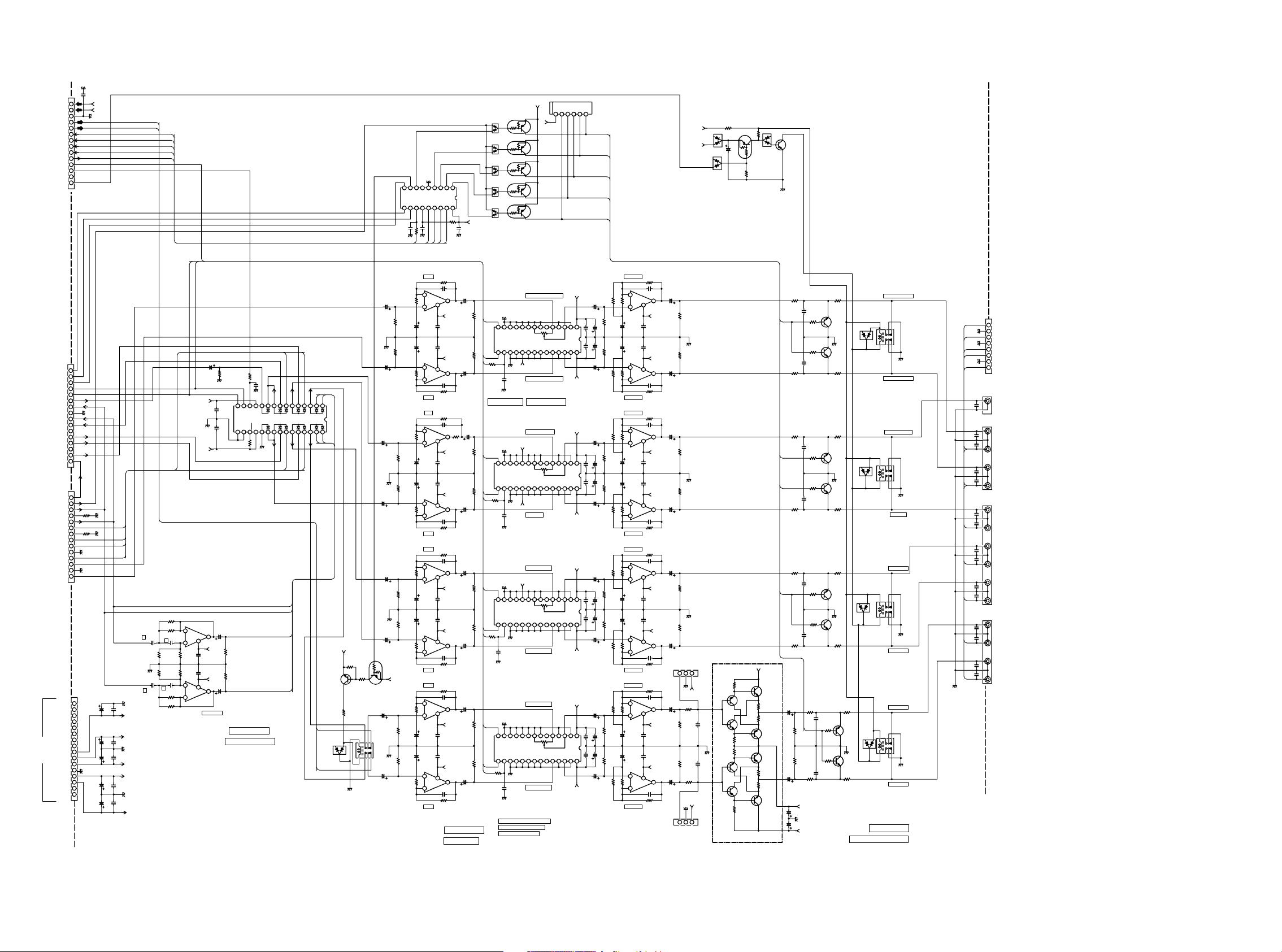
JC01
TUNER-L
TUNER-R
GND
L(OUT)
R(OUT)
M06-CONNECT
TAPE-MUTE
VCR-MUTE
MULTI-MUTE
CDR/MD-MUT
CE6(P.EXP)
CEX(LRG/SML)
CE0(ANA.SW)
CE3(TONE)
MUTE-RELAY
DATA 0
CLK0
OSD-OUT
VD ATA
VCLK
M02-6CH IN
TO JC71 (PL04)
_KILLCON
_KILLCON
ERMUTE
M08-DSP
TO J601 (P604)
SBL-D
SBR-D
OSD-INT
CE7(P.EXP)
CE2(OSD)
CE1(OSD)
SYNC DET2
SYNC DET1
COMMON BUS
JC03
FL-D
FR-D
SW-D
SL-D
SR-D
-15VA
SWA
GND
SL6
GND
C-D
GND
GND
GND
+15VA
DATA 0
FL
GND
FR
SW6
C6
SR6
GND
JC02
OSD-2
OSD-1
-24V
+5VV
+5VL
GND
CLK0
JC04
ELE.VOL/MUTE CIRCUIT BLOCK
CEX
SWD
SLD
RC40
22/16V
15V-6
8
4
80HZ HPF
A7
CC40
CC06
CC05
7
-15V-5
1
47K
A7
0.01
CC25
CC26
CC08
10/50V
+15VA
15V-6
0.01
0.01
-15VA
CC07
10/50V
CROSS OVER
RC32
100
CC27
A7
15 14 13 121110
VEE VDD
CEDICL
QC01
LC78213
FUNC.
RES
VSS
S
0.01
16 17 18 192021
RC33
100K
A7
RC10
100K100K
RC09
RCR-XCXX
CH
100P
6CH
DIG
98765432
SW
22 23 24 25 26 27 28 29
6CH
ANA
DIG
CD
R-L
L-L
R-S
L-S
SL OUT
FL OUT
FL IN
6CH
DIG
L-L
L-S
1
FL
FRSLSRCENTER
30
R-S
DIG
6CH
FR IN
SR OUT
C OUT
FR OUT
SRD
RT
LT
SW OUT
R-L
RB425D
QC07
2SC2120
RC36
100
1/2W
DC01
+5VL
5V-4
QM09
DTA114ES
/UN4111
/KRA102M
-15VA
121314
QG51
TC9459N
NC
NC
A7
CG73
100P
CH
121314
QV03
TC9459N
NC
NC
A7
CV93
100p
CH
121314
QV02
TC9459N
NC
NC
A7
121314
QV01
TC9459N
NC
NC
A7
CV23
100p
CH
+15VA
15V-6
-15V-5
QM10
DTA114ES
/UN4111
/KRA102M
QM11
DTA114ES
/UN4111
/KRA102M
QM12
DTA114ES
/UN4111
/KRA102M
QM13
DTA114ES
/UN4111
/KRA102M
SURR.BACK RCH
NC
CS1NCNC
LD1
LD2NCCS2
202122 23 24
15V-6
+15VA
SURR.BACK LCH
RVR-XGXX
SUB WOOFER
NC
CS1NCNC
LD1
LD2NCCS2
202122 23 24
+15VA
15V-6
CENTER
SURR. RCH
+15VA
15V-6
NC
CS1NCNC
LD1
LD2NCCS2
202122 23 24
SURR. LCH
FRONT RCH
NC
CS1NCNC
LD1
LD2NCCS2
202122 23 24
FRONT LCH
NC
NC
25 26 27
NC
NC
25 26 27
NC
NC
25 26 27
NC
NC
25 26 27
DM05
1SS200
DM06
1SS200
ANA/_DIG
QM17
NJU3713D
CG76
22/25V
A7
CG75
22/25V
CV96
22/25V
A7
CV95
22/25V
CV66
10/25V
A7
-24V-2
-24V
RC35
CV65
10/25V
10K
5V-4
RC34
+5VL
QC08
10K
DTA114ES
/UN4111
/KRA102M
CV26
22/25V
LC01
ED2-24
A7
CV25
22/25V
A7
OSD-OUT
P11
P12
P10
CK
CLR
STB
DATA
101112 13 14 15 16 17 18
CH
CM09
100P
A9
A9
RM55
CE6
100
+6DB
CG56
2
-
3
10K
RG54
+
47K
RG74
CG52
CG51
47K
RG73
5
+
10K
RG53
6
-
CG55
+6DB
0DB
CV76
2
-
3
RV74
DAMMY
+
CV72
CV71
47k 47k
RV93 RV94
5
+
6
10k
-
RV73
CV75
+6DB
+6DB
CV46
2
-
10k
RV44
3
+
47k
RV64
CV42
CV41
47k
RV63
5
+
6
10k
-
RV43
CV45
+6DB
+6DB
CV06
-
2
10k
RV04
+
3
47k
RV24
CV02
CV01
47k
RV23
+
5
10k
RV03
-
6
CV05
+6DB
A9
VSS
P1P2P3
CM10
T-M
100P
10/50V
10/50V
DAmmY
10/50V
10/50V
10/50V
10/50V 10/50V
1
23456789
P5P6P7P8P9
P4
VDD
RM46
25V
1K
0.1
A9
V-M
M-M
MD-M
RG56
10K
CH
QG52-2
22/25V
1
VSS
4
-15VA
-15V-5
CG54
0.01
CG53
0.01
+15VA
15V-6
QG52-1
8
NJN2114
7
VCC
22/25V
100P
CH
RG55
10K
RV76
0
100p
CH
QV07-2
1
VSS
RV89
4
100
-15V-5
-15VA
CV73 CV74
0.01 0.01
+15VA
15V-6
QV07-1
8
NJM2114
7
VCC
100p
CH
RV75
10k
RV46
10k
100p
CH
1
VSS
4
QV06-2
-15V-5
-15VA
CV44
0.01
CV43
0.01
+15VA
15V-6
QV06-1
8
NJM2114
7
VCC
100p
CH
RV45
10k
RV06
10k
100p
CH
22/25V
QV05-2
1
VSS
4
-15V-5
-15VA
0.01
CV04
CV03
0.01
+15VA
15V-6
QV05-1
8
NJM2114
VCC
7
100p
CH
RV05
10k
RVR-XVXX
ELE.VOL
CG58
CG57
22/25V
22/25V
22/25V
CV08
CV07
22/25V
CM11
RG58
RG57
CV78
22/25V
RV78
RV77
CV77
CV48
RV47 RV48
CV47
+5VL
5V-4
25V
0.1
47K
47K
47k
47k
47k 47k
47k 47k
RV07 RV08
DM07
1SS200
DM08
1SS200
DM09
1SS200
A7
VCLK
GND
CK
DATA
STB
15 16 17 18 19
VDATA
CEX
RG70
100
A7
ELE.VOL
A7
VCLK
GND
CK
DATA
STB
15 16 17 18 19
VDATA
CEX
RV90
100
A7
A7
VCLK
GND
CK
DATA
STB
15 16 17 18 19
VDATA
CEX
RV60
100
CV63
100p
CH
A7
A7
VCLK
GND
CK
DATA
STB
15 16 17 18 19
VDATA
CEX
RV21
100
A7
XV7X-XV9X:SBLorSBR
XV4X-XV6X:SLorSR
XV0X-XV3X:LorR
-15V-5
RM54
RM51
100
RM52
470/16V
0.6
-0.6
RV34
10k
RV33
10k
-0.6
0.6
10K
QM16
DTA114EKA
RM53
22K
+15VA
2SC2240
0
0
2SA970
0
RV35
2SC2240
0
DM10
RB425D
15V-6
QV18
RV36
22
RV38
22
QV20
2SA970
QV19
RV37
22
22
QV17
A8
SB MUTE
SW MUTE
C MUTE
S MUTE
22/10V
22/50V
QM15
2SA1837
RM32
330
RM31
330
RM22
330
RM21
330
RM12
330
RM11
330
CV32
RV26
100k
RV25
100k
CV31
-15V-5
-15VA
EA2230
22/25V
CV29
22/25V
15V-6
+15VA
CM07
CM06
CM05
CM04
CM08
CH
470P
CM03
F MUTE
CH
470P
CH
470P
CH
470P
CH
470P
A7
CH
470P
RM01
330
RM33
4.7K
RM23
4.7K
RM14
4.7K
RM13
4.7K
RM02
CM02
CM01
RM34
4.7K
RM24
4.7K
330
CH
470P
CH
470P
-13.7
RM04
4.7K
-13.7
RM03
4.7K
RM36
150
QM08
2SC3326
(A,B)
A7
QM07
2SC3326
(A,B)
RM35
150
RM26
150
QM06
2SC3326
(A,B)
A7
QM05
2SC3326
(A,B)
RM25
150
RM16
150
QM04
2SC3326
(A,B)
A7
QM03
2SC3326
(A,B)
RM15
150
0
RM06
150
0
2SC3326
(A,B)
2SC3326
RM05
SURR.BACK R
LM04
DM04
MR82
1SS356
SURR.BACK L
SUB WOOFER
LM03
DM03
MR82
1SS356
DM02
1SS356
DM01
QM02
1SS356
A7
QM01
(A,B)
150
RMT-XMXX
MUTE CONTROL
CENTER
SURR. R
SURR. L
FRONT R
FRONT L
JM04
FL
8
FL
A7 A7 A7
7
GND
SR
6
SR
M01-AMP
5
GND
CNT
A7
FR
SL
TO J701 (P704)
4
CNT
3
FR
2
GND
1
SL
M01-AMP
TO JP01 (P754)
JM05
SW
CM28
220P
CH
JM03
CM27
220P
CH
FRFR
CM35
470P
CH
CM26
220P
CH
FL
FL
CM34
470P
A7
LM02
MR82
A7
LM01
MR82
A7
CH
CM25
220P
CH
CNT
CM33
470P
CH
CM24
220P
CH
SR
CM32
470P
CH
CM23
220P
CH
SL
CM31
470P
CH
CM22
220P
CH
FR
CM30
470P
CH
CM21
220P
CH
FL
CM29
470P
CH
A7
JM02
JM01
PRE-OUT
SBR
MAIN-IN
PRE-OUT
SBL
MAIN-IN
PRE-OUT
CENTER
MAIN-IN
PRE-OUT
SR
MAIN-IN
PRE-OUT
SL
MAIN-IN
PRE-OUT
FR
MAIN-IN
PRE-OUT
FL
MAIN-IN
SB MUTE
SW MUTE
C MUTE
F MUTE
S MUTE
RG66
+12.4DB
8.2K
100P
CH
47/25V
CG72
47/25V
CG71
CV92
47/25V47/25V47/25V
CV91
CV62
CV61
47/25V
CV22
47/25V 47/25V
CV21
47K
RG60
47K
RG59
1.5k
RV82
47k47k
RV80
RV79
47k
RV50
47k
RV49
5.6k
RV51
5.6k
RV12
RV10
47k 47k
RV09
5.6k
RV11
5.6K
RG62
5.6K
RG61
5.6k
RV81
5.6k
RV52
4.7K
RG64
4.7K
RG63
1.8k
RV84
4.7k
RV83
4.7k
RV54
4.7k
RV53
4.7k
RV14
4.7k
RV13
CG66
2
-
3
+
CG62
10/50V10/50V
CG61
5
+
6
-
CG65
+12.4DB
+22.4DB
CV86
2
-
3
+
CV82
47/50V
CV81
10/50V
5
+
6
-
CV85
+12.4DB
+12.4DB
CV56
2
-
3
+
CV52
CV51
5
+
6
-
CV55
+12.4DB
+12.4DB
CV16
2
-
3
+
CV12
10/50V
CV11
10/50V
5
+
6
-
CV15
+12.4DB
VSS
VCC
VSS
VCC
VSS
10/50V 10/50V
VCC
VSS
VCC
100P
100p
100p
100p
100p
100p
100p
QG53-2
4
8
RG65
8.2K
RV86
10k
QV11-2
4
8
RV85
8.2k
QV10-2
4
8
RV55
8.2k
RV16
8.2k
QV09-2
4
8
RV15
8.2k
CG64
0.01
CG63
+15VA
NJM2114
CH
CH
-15VA
-15V-5
CV84
CV83
+15VA
15V-6
QV11-1
NJM2114
CH
RV56
8.2k
CH
-15VA
-15V-5
CV53 CV54
QV10-1
NJM2114
CH
CH
-15V-5
-15VA
CV13 CV14
+15VA
NJM2114
CH
-15VA
-15V-5
0.01
15V-6
QG53-1
7
0.01
0.01
7
+15VA
7
0.01 0.01 0.01 0.01
15V-6
QV09-1
7
-15VA
-15V-5
CG60
22/16V
25V
0.1
1
234567891011
NC
VSS
CG70
VDD
25V
NC
28
0.1
CG69
CG59
22/16V
15V-6
+15VA
-15VA
-15V-5
CV80
22/16V
25V
0.1
1
234567891011
NC
VSS
CV90
VDD
NC
25V
28
0.1
CV89
CV79
22/16V
15V-6
+15VA
-15VA
-15V-5
CV50
22/16V
25V
0.1
1
234567891011
NC
VSS
CV60
VDD
NC
25V
28
0.1
CV59
CV49
22/16V
15V-6
+15VA
-15VA
CV10
22/16V
25V
0.1
1
234567891011
NC
VSS
CV20
VDD
NC
25V
28
0.1
CV19
CV09
22/16V
15V-6
+15VA
-24V-2
+5VL
5V-4
DM11
RB425D
CM12
DM12
RB425D
CG68
47/16V
1
47K47K
RG68RG67
A7
CG67
47/16V
CV88
47/16V
1
47k
RV88
A7
47k
RV87
CV87
47/16V
CV58
47/16V
1
47k
RV58
A7
47k
RV57
15V-6
CV57
47/16V
1
CV18
47/16V
1
CV17
47/16V
1
JV02
DAMMY
23
A7
RV20
470
RV18RV17
RV19
470
A7
23
JV01
DAMMY
-15V-5
47k47k
-15VA
15V-6
+15VA
CV27 CV28
010K (HDAM CASE)
RV32
10k
QV14
2SA970
0
CH
QV16
100p
2SC2240
A7
QV15
2SC2240
CH
0
100p
QV13
2SA970
RV31
10k
HDAM BLOCK
1/2W
-24V
R LARGE
L LARGE
M
M
CC02
A7
CC01
LT
RT
T-M
V-M
M-M
MD-M
CE6
RC02
RC04
0.1
M
CC04
RC06
RC05
CC03
M
RC03
0.1
DAMMY
RC01
P104-2/2
VCLK
VDATA
-15V-5
-15VA
+15VA
12K
6
QC03-2
-
DAMMY
5
+
0.1
27K
27K
RC07 RC08
DAMMY DAMMY
0.1
+
3
2
-
QC03-1
NJN4558DD
12K
CC41
DAMMY
TUN-L
1
TUN-R
2
A7
3
4
5
6
7
8
9
10
11
12
13
14
1
2
3
4
5
6
7
8
9
10
11
12
13
14
15
16
1
2
3
4
5
6
7
8
9
10
11
12
13
14
1
2
3
4
5
6
7
8
9
10
11
12
13
14
15
16
A7
RC11
DAMMY
RC12
DAMMY
A7A7
A9
CC31
100/25V
CC28
DAMMY
CC29
100/10V
CC30
100/10V
CC32
100/25V
TUNER-BLOCK
P104
A7
A7
CD
SWD
SLD
SRD
R SMALL
L SMALL
A7
0.1
25V
CC33
-24V
-24V-2
+5VV
5V-3
0.1
25V
CC34
A7
0.1
25V
CC35
+5VL
5V-4
-15VA
-15V-5
0.1
25V
CC36
A7
0.1
25V
CC37
+15VA
15V-6
17 18
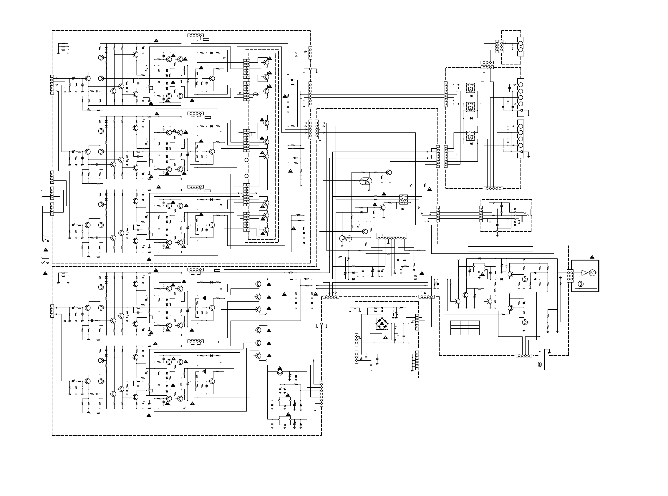
5
FL
4
GND
3
RS
2
GND
(M02-PRI OUT)
TO JL08 (PL04)
1
CNT
J715
1
2
3
M04-PRIMARY
TO JB12 (PB04)-U.F
TO JB62 (PB54)-K.N,S
J716
1
2
3
J717
1
2
3
W702
W703
ON 2CH
HEATSINK
S702
TEMP-SW
120B
ON 3CH
HEATSINK
S701
TEMP-SW
120B
1
LS
2
GND
3
FR
M02-PRE OUT
TO JL11 (PL04)
MAIN-IN
J701
TEMP OUT
N.C
+24V
(RMA)
P704
MAIN-IN
JP01
*
R789
10
R790
10
RT89
10
C701
47/10V
R701
220k
C702
47/10V
R702
220k1k33k
CT01
47/10V
RT01
220K
(M01)
RP89
10
RP90
10
CP01
47/10V
RP01
220K1K33K
CP02
47/10V
RP02
220K
R703
R717
4.7k
R704
R718
4.7k
RT03
RT17
4.7K
RP03
RP17
4.7K
RP04
RP18
4.7K
R705
33k
R706
33K
RP05
RP06
33K
1k
RT05
1K
0
C703
470P
R711
R707 R709
1.5k 1.5k
R715
100K
C704
470P
R712
R708
1.5k 1.5k
R716
100K
1K
CT03
470P
RT11
RT07 RT09
1.5K 1.5K
RT15
100K
CP03
470P
CP05
470P
RP07 RP09
1.5K 1.5K
RP15
100K
QP02
2SA970
CP04
470P
RP12
RP08
1.5K 1.5K
RP16
100K
2SA1145
Q701
2SA970
2SA970
-62.4
220
2SA1145
Q702
2SA970
2SA970
220
2SA1145
QT01
2SA970
2SA970
220
2SA1145
QP01
2SA970
2SA970
2SA1145
QP04
2SA970
220
R713
Q705
O/Y
Q703
R714
Q706
O/Y
Q704
RT13
QT05
O/Y
QT03
RP13
QP05
O/Y
QP03
RP14
QP06
O/Y
R710
RP10
270
63.4
C705
470p
270
C706
470p
270
CT05
470p
270
RP11
220
270
CP06
470P
0.6
R719
4.7k
R720
4.7k
RT19
4.7K
RP19
4.7K
RP20
4.7K
J713
1
234
R775 R779
1k
R773
0.10 X2
J714
*
1
234
R776
1k
R774
1
234
RT75
1K
RT73
1
234
RP75 RP79
1K
RP73
1
234
RP76
1K
RP74
BIAS
5W
R777R778RT77RP77RP78
BIAS
5W
0.10 X2
BIAS
5W
0.10 X2
5W
0.10 X2
5W
0.10 X2
2.2k2.2k2.2K2.2K2.2K
JT13
JP03
JP04
*
D721
HSS81
Q729
0
C721
D722
HSS81
Q730
C722
*
DT21
HSS81
CT21CP21
*
DP21
HSS81
QP29 QT29
*
DP22
HSS81
QP30
CP22
63.8
0
0.010.010.010.010.01
BIAS
BIAS
2SC2240 2SC2240 2SC2240 2SC2240 2SC2240
22k
R781
22k
R780
22k
R782
22k
RT79
22K
RT81
22K
22K
RP81
22K
RP80
22K
RP82
22K
J709
J708
J707
+B
J706
-B -B
C.DET
SL
SR
11
33
55
11
33
55
1
33
55
616
11
33
55
66
J705
11
44
55
J785
22
44
J784
22
44
PTH9M04BE222TS
P774
J783
+B
22
44
J710
J711
J782
22
44
J781
22
33
-0.5
0.4
-1.0
D799
63.9
1.6
-1.6
0
-64.1
(M01)
+B
-B
QP25
QP15
QP27
QP26
QP16
QP28
0
+B
Q715
2SC3419Y
Q727
2SA1216
-B
Q726 Q725
2SC2922 2SC2922
Q716
2SC3419Y
2SA1216
QT25 Q728
2SC2922
+B
QT15
2SC3419Y
-B
QT27
2SA1216
+B
2SC2922
2SC3419Y
2SA1216
-B
+B
2SC2922
2SC3419Y
2SA1216
-B
Q881
2SC4793
11.0
C882 D882
100/6.3V
C862
0.01
11.0
C872
0.01
11.0
4.1
5VREG
5VREG
Q861
Q871
R787
56k
220 1/4W
3.5
3.9V
L701
R783
220 1/4W
R785
10
C723
0.1
C725
0.1
R788
56k
RT87
56K
220 1/4W
LP01
RP83
RP85
10
1W
CP23
0.1
CP25
0.1
C881
100/16V
100/16V
5.0
100/16V
5.0
J703
1
TO J854(P854)
+B
2
+B
-B
M06-SUPPLY
3
-B
J712
J702
7
FL
6
5
RS
4
1W
3
C C
2
1
(M01)
P754
(RMB)
(RMC)
C.DET
J704
JN04
5
5
L
4
4
3
3
2
2
1
1
L702
R784
R786
10
C724
0.1
C726
0.1
220 1/4W
10
R881
100
1/4W
C861
1W
RT83
RT85
CT23
0.1
CT25
0.1
H/P-ON :H
H/P-OFF:L
LT01
1W
LP02
MUTE-RLY
RN03
56K
RN02
56K
CN05
100/16V
RN14
47K
RN13
6.8K
8.9
QN02
DTC144ES
0
CN06
100/16V
RN01
2.2K
DN01
DN02
22/50V
*
*
+B
RP84
220 1/4W
-B
RP86
JN03
10
CP24
0.1
CP26
0.1
1W
234
NC
H.P.SW
RELAY CTRL
TO JY68 (PY64)
M06-CONNECT
1
J855
MUTE-RLY
JP05
J854
M01-AMP
GND
2
+B
3
-B
TO J703(P704)
1
J851
3
M04-AUDIO
2
1
D881
J871
7
+12V
6
+3.3V
5
+5VV
4
+5VA.D
3
+8V
+8V
2
1
GND
FROM MAIN TRANSF.
(AC)
TO J806 (PS04)
12V
1D3
D861
1D3
0
DTC144ES
RN15
47K
CN10
2SA970
64.0
RN11
2.2K
CN04
QN05
QN03
0.1
DN10
HSS81
RN10
47K
C854
0.01
500V
RN46
RN45
64.0
-0.6
CURNT-DET
CN03
0
47/16V
R852
RN18RN17
10K10K
0.6
RN19
47K
330
1W
330
1W
12.1
RN16
0
QN04
RN48
2SD1508
47K
RN12
TA7317P
47K
RELAY DRIVER
1
23456789
0
0
-0.6
RN09
47K
0.1
CN02
47/16V
CN01
R851
D853
4.7k
4.7k
D854
R853
D851
D25XB60
C851
C851
0.01
500V
C852
0.01
P854
500V
(RPB)
0.1
QN06
2SC1627
O/Y
LN01
MR62-12USR
10
DN03
1D3
QN01
0
0
0.7
3.0
1.3
-0.7
RN06
47K
CN07
RN07
1/50V
120K
CN09
CN08
100/10V
0.1
R854
1D3
150k
1D3
C857
10k
2.2/50V
64.0
C853
56000
71V
C854
0.01
(C854, C855 : F, K, U only)
(M06)
C855
0.22
+12V
RN08
33K
1/4W
RN05
33K
RN04
1/2W
15K
RN20
1K
RELAY+B(+62V)
J852
*
-0.6
1
2
3
+B
4
-B
-64.1
J853
1
2
3
4
5
C871
D871
1D3
RN44
220
H.P SW
1
2
34
M06-SPK
TO JN52 (PT04)
JN05
FR FR
4
3
RELAY
2
+B
1
1W
JN08
*
L
4
GND
3
R
2
1
RN21
POW-H:H
47K
POW-L:L
CN11
10/50V
JN02
*
1
2
3
1
23
1
23
JN56
JN51
7
FL
6
5
RS
4
3
2
1
JN53
66
55
4
LSLS
3
2
1
DN53
LN53
LN51
18V
LN52
18V
DN52
18V
DN51
1D3
1D3
1D3
EH 4P
JW02
*
4
3
2
1
L
GND
R
H.P SW (H)
C-G
SL-G
RS-G
1
245
3
TO J853(P854)
M06-SUPPLY
CW04
0.1
WW01
FR-G
COOLING FAN CONTROL
DN04
+12V +12V
CN14
100/16V
RN23
47K
RN22
1K
1W<:L
1W>:H
QN08
2SC536
0.6
SP/ETC
0
FAN CONDITIONS
TEMP.
POW.
HI
HI
HI
LO
LO STOP
LO/HI
*FAN VOLTAGE
FAST:11.5V
SLOW:7.5V
STOP:0V
1
12.1
RN24
10K
POW-H:H
POW-L:L
0
QN09
2SC536
SP/ETC
FAN
FAST
SLOW
*POW.RATE
STEREO(2-CH)
HI:>35W X 2
5-CH DRIVE
HI:>5.5W X 5
QN07
REG
12V/7.5V
3
RN25
2.2K
CN12
1D3
47/16V
2SC536
SP/ETC
QN10
2
0.4
4
0
47/16V
2.8
CN17
RN27
3.9K
RN26
33K
RN28
120
10
RN29
2.2K
R749
10
1/4W
D701
R727
R731
R735
560 560
*
D703
*
62.6
R721
56k
R723
56k
0
-62.4
O/Y
Q707
2SC2705
D702
*
D704
*
R722
56k
R724
56k
O/Y
Q708
2SC2705
DT01
*
DT03
*
RT21
56K
RT23
56K
O/Y
QT07
2SC2705
DP01
*
DP03
*
RP21
56K
RP23
56K
O/Y
QP07
2SC2705
DP02
*
DP04
*
RP22
56K
RP24
56K
O/Y
QP08
2SC2705
62.9
62.9
O/Y
Q709
2SC2705
63.0
R725 R729
560 560
R728 R732
560 560
O/Y
Q710
2SC2705
R726
560 560
RT27
560 560
O/Y
QT09
2SC2705
RT25 RT29
560 560
RP27
560 560
O/Y
QP09
2SC2705
RP25 RP29
560 560
RP28 RP32
560 560
O/Y
QP10
2SC2705
RP26
560 560
R730
RT31
RP31
RP30
56
63.5
C713
C727
220/100V
R753
Q711
100
10
10
10
10
10
10
10
R751
10
C714
R752
RT51
RP49
CP13
RP51
RP50
CP14
RP52
R745
2.2k
1/4W
R750
1/4W
220/100V
R746
2.2k
1/4W
RT49
10
1/4W
RT45
2.2K
1/4W
1/4W
220/100V
RP45
2.2K
1/4W
1/4W
220/100V
RP46
2.2K
1/4W
R747
R743
2.2K
R748
47K
R744
2.2K
RT47
47K
RT43
2.2K
RP47
47K
RP43
2.2K
RP48
47K
RP44
2.2K
1.6
Q717
2SC2705
O/Y
D713
HSS81
47K
D717
5.1V
D715
HSS81
D719
5.1V
-1.6
R755
100
C729
C728
R754
100
Q718
2SC2705
O/Y
D714
HSS81
D718
5.1V
D716
HSS81
D720
5.1V
R756
100
C730
CT27
RT53
100
QT17
2SC2705
O/Y
DT13
HSS81
DT17
5.1V
DT15
HSS81
DT19
5.1V
RT55
100
CT29
CP27
RP53
100
QP17
2SC2705
O/Y
DP13
HSS81
DP17
5.1V
DP15
HSS81
DP19
5.1V
RP55
100
CP29
CP28
RP54
100
QP18
2SC2705
O/Y
DP14
HSS81
DP18
5.1V
DP16
HSS81
DP20
5.1V
RP56
100
CP30
2SA1360
1.5
C715
‚PƒÊ‚e
100V
R741
12k
R739
33k
R737
62.9
1.2k
C717
10p/250V
C707
470/6V
-1.6
Q713
-62.8
2SC3423
-63.6
R733
56
C711
220/100V
R736
56
Q712
2SA1360
C716
‚PƒÊ‚e
100V
R742
12k
R740
33k
R738
1.2k
C718
10p/250V
C708
470/6V
Q714
2SC3423
R734
56
C712
220/100V
CT13
220/100V
RT35
56
QT11
2SA1360
CT15
1UF
100V
RT41
12K
RT39
33K
RT37
1.2K
CT17
10p/250V
CT07
470/6V
QT13
2SC3423
RT33
56
CT11
220/100V
RP35
56
QP11
2SA1360
CP15
1UF
100V
RP41
12K
RP39
33K
RP37
1.2K
CP17
10P/250V
CP07
470/6V
QP13
2SC3423
RP33
56
CP11
220/100V
RP36
56
QP12
2SA1360
CP16
1UF
100V
RP42
12K
RP40
33K
RP38
1.2K
CP18
10P/250V
CP08
470/6V
QP14
2SC3423
RP34
56
CP12
220/100V
120p
120p
120p
120p
120p
120P
120P
120p
120P
120P
63.9
1.0
1.0
R761
1k
1/6W
R767
1/2W
-1.0
1.0
Q719
2SA1145
O/Y
-64.1
R762
1k
1/6W
Q720
2SA1145
O/Y
RT61
1K
1/6W
RT67
1/2W
QT19
2SA1145
O/Y
RP61
1K
1/6W
RP67
1/2W
QP19
2SA1145
O/Y
RP62
1K
1/6W
RP68
1/2W
QP20
2SA1145
O/Y
R763
220
R765
R764
R768
220
1/2W
R766
RT63
220
RT65
RP63
220
RP65
RP64
220
RP66
+B
Q721
2SC4793
0.4
22
2.2
R769
C719
4.7/100V
22
-0.4
2.2
R771
Q723
2SA1837
-B
+B
Q722
2SC4793
2.2
22
R770
C720
4.7/100V
22
2.2
Q724
2SA1837
-B
+B
QT21
2SC4793
2.2
22
RT69 R772
CT19
4.7/100V
22
2.2
RT71
QT23
2SA1837
-B
+B
QP21
2SC4793
22
2.2
RP69
CP19
4.7/100V
22
2.2
RP71
QP23
2SA1837
-B
+B
QP22
2SC4793
22
2.2
RP70
CP20
4.7/100V
22
RP72
2.2
QP24
2SA1837
-B
JN72
1
2
3
PT74
PT04
(RSP)
CN55
0.01
CN57
0.01
CN52
0.01
CN56
0.01
CN58
0.01
N,S ONLY
CN51-CN58
JN52
FL-G
CW01
0.01
CW02
0.01
CW03
0.1
CN13
100/16V
DN05
*
12.1
-0.6
RN43
22K
CN71
0.01
N,S ONLY
(M06)
CN51
0.01
CN53
0.01
CN54
0.01
OFF
ON
CN15
0.1
RN30
10K 10K
4.1
QN11
3.3
2SC2240
SP/ETC
+12V
JN71
(M06)
N,S ONLY
CW01-CW03
PW04
TEMP-H:L
TEMP-L:H
RN31
4.7K
2SC2240
RN42
22K
12.1
QN14
2SA608
SP/ETC
LOCK
FAN
1
CENTER
GND
JN54
FL-CH
GND
GND
LS-CH
JN55
FR-CH
GND
GND
RS-CH
JW01
L
R
(RHP)
(M07)
RN32
3.9
0
QN12
SP/ETC
CN16
470/6V
RN41
220K
11.9
QN13
2SC536
SP/ETC
TEMP.3CH
TEMP.2CH
FAN SPEED
234
JN10
PTH9M04BE222TS
0
DN06
*
DN07
*
RN33
47K
DN09
POSISTOR
RN36
100
RN35RN34
RN37
RN40
2.2K
MN51
12V FAN
JN09
22K22K
*
DC-IN
1
1
GND
2
2
3
3
STOP
100
RN49RN38
2.2K10K
19 20
PB04 P.C.Board
PRIMARY
U version
SWITCHED
JB03
PRIMARY BLOCK
RB05
CB03
0.01
JB04
3123
12
GND
RELAY
TO J715 (P704)
+24V
M01-AMP
2.2 7W
RB02
2.2 7W
DB01
1D3
+24V
N.C
RB03
47K
DTA114ES
TO J804 (PS04)
VS24MB-NR
DB02
1D3
CB02
100/10V
RB04
10K
QB01
/ETC
M04-AUDIO
LB03
QB02
2SC3419Y
TO J805 (PS04)
M04-AUDIO
21345
678
BLUE
BLUE
YELLOW
YELLOW
ORANGE
ORANGE
GRAY
BLACK
QB52
CB53
0.01
JB54
3123
12
GND
+24V
RELAY
TO J715 (P704)
P.C.Board
RB55
2.2 7W
RB52
2.2 7W
DB51
VS24MB-NR
1D3
T6.3A 250V
N.C
+24V
M01-AMP
PRIMARY
AC.OUTLETS
UNSWITCHED
PB04
(M04)
(RBU)
JB08
WHITE
12
12
**
RED
RB01
2.2M
1/2W
L003
JB09
ORG
12
RED
JB07
RED
PB74
JB71
12
CB01
0.01
LB02
VS24MB-NR
JB01
*
FB01
12A 250V
JB02
*
JB12
12
12
TEMP OUT
RED
L001 L051
TS42002100 TS42002080
FB02
630MA 250V
12
JB05 JB06
WHITE
WHITE
JB10JB11
FERITE CORE
J001
TS16404120
SUB-TRANSF.
(M05)
(RSW)
SB71
CB71
0.01
AC9.7V AC9.7VAC20V AC20V
L002
AC5.1V
Z007
AC120V 60HZ
PB54
K version
PRIMARY BLOCK
LB53
VS24MB-NR
DB52
1D3
2SC3419Y
CB52
100/10V
RB54
RB53
10K
47K
QB51
DTA114ES
/ETC
TO J804 (PS04)
M04-AUDIO
LB52
FB51
JB62
TEMP OUT
CB51
0.01
JB51
JB52
12
12
BRN
PB54
JB11 JB10
JB55
BLU
(M04)
(RBU)
JB58
JB59
FB52
T200MA 250V
**
12
JB56
BLU
BRN
12
12
BRN
12
BRN
JB57
BLU
BRN
PB74
JB71
12
ORANGE
J051
TO J805 (PS04)
M04-AUDIO
678
YELLOW
ORANGE
GRAY
AC9.7V AC9.7VAC20V AC20V
L052
TS17205090
SUB-TRANSF.
(M05)
(RSW)
SB71
CB71
0.01
21345
BLUE
BLUE
YELLOW
BLACK
AC5.1V
Z007
AC220V 50/60HZ
AC62V AC62V AC20V AC20V
PB54
PRIMARY
REDBLK ORG YEL GRYGRN N.C
123
TO J851 (P854)
M06-SUPPLY
P.C.Board
123
TO J801(P804)
M05-SUPPLY2
4
TO J805 (PS04)
M04-AUDIO
21345
678
BLUE
BLUE
YELLOW
YELLOW
ORANGE
ORANGE
GRAY
BLACK
PB04 P.C.Board
N,S version F version
Z007
AC5.1V
AC230V 50HZ
PRIMARY BLOCK
RB03
47K
PRIMARY BLOCK
LB53
RB53 RB54
47K 10K
QB51
DTA114ES
/ETC
VS24MB-NR
DB52
1D3
CB52
100/10V
TO J804 (PS04)
M04-AUDIO
QB52
2SC3419Y
CB53 RB52
0.01 2.2 7W
12
RELAY
RB55
2.2 7W
DB51 LB52
1D3
JB54
3123
GND
+24V
+24V
TO J715 (P704)
M01-AMP
VS24MB-NR
FB51
T6.3A 250V
JB62
N.C
TEMP OUT
CB51
0.01
JB51
JB52
12
12
BRN
L051
TS42002090
PB54
JB11 JB10
**
JB55
BLU
(M04)
(RBU)
FB52
T200MA 250V
12
BLU
FERITE CORE
AC9.7V AC9.7VAC20V AC20V
L052
BLU
BRN
PB74
12
J051
TS17205100
SUB-TRANSF.
(M05)
(RSW)
SB71
CB71
0.01
JB58
12
12
JB71
JB59
BRN
12
BRN
JB57
JB56
BRN
L053
PRIMARY
LB03
VS24MB-NR
DB02
1D3
CB02
100/10V
RB04
10K
QB01
DTA114ES
/ETC
TO J804 (PS04)
M04-AUDIO
QB02
2SC3419Y
SWITCHED
CB03
0.01
JB04
3123
12
GND
RELAY
TO J715 (P704)
AC62V AC62V AC20V AC20V
REDBLK ORG YEL GRYGRN N.C
123
TO J851 (P854)
M06-SUPPLY
AC.OUTLETS
JB03
RB05
2.2 7W
RB02
2.2 7W
DB01
VS24MB-NR
1D3
JB12
N.C
+24V
+24V
TEMP OUT
M01-AMP
LB02
TO J801(P804)
M05-SUPPLY2
CB01
0.01
JB01
*
FB01
12A 250V
JB02
*
12
12
RED
L001
TS42002070
123
4
UNSWITCHED
PB04
JB11 JB10
**
JB05
WHITE
FB02
630MA 250V
12
WHITE
(M04)
(RBU)
RED
JB06
JB08
JB09
12
12
ORG
12
RED
JB07
WHITE
RED
PB74
JB71
12
(RSW)
TO J805 (PS04)
ORANGE
GRAY
(M05)
SB71
CB71
0.01
M04-AUDIO
678
YELLOW
ORANGE
BLACK
AC9.7V AC9.7VAC20V AC20V
L002
TS17205110
SUB-TRANSF.
21345
BLUE
BLUE
YELLOW
AC5.1V
Z007
AC100V 50/60HZ
AC62V AC62V AC20V AC20V
REDBLK ORG YEL GRYGRN N.C
123
TO J851 (P854)
M06-SUPPLY
123
TO J801(P804)
M05-SUPPLY2
AC62V AC62V AC20V AC20V
4
REDBLK ORG YEL GRYGRN N.C
123
TO J851 (P854)
M06-SUPPLY
123
TO J801(P804)
M05-SUPPLY2
4
21 22
RF OR DIG.6
INPUT
DIGITAL
INPUT-5
COAX
DIGITAL
INPUT-4
DIGITAL
INPUT-3
OPT
DIGITAL
INPUT-2
OPT
DIGITAL
INPUT-1
OPT
DIGITAL-OUT
JR05
COAX
DIGITAL-OUT
JR06
JE01
CE13
0.1
SMUTE
_RSTDA1
_RSTDA2
FS96
DEEMP
_ATT
CAL
_RSTAD
100/10V
100/10V
SEL1
1A
1B
1Y
2A
2B
2Y
GND 3Y
Q693
S-807
4.5V
C696
0.01
50V
C602
0.01
C605
0.01
C624
0.1
16V
Q602
TC7WT241FU
G
VCC
A1
G
Y2
Y1
GND
A2
5DP
VCC
ST
4A
4B
4Y
Q603
BP SW
3A
TC74HC157AF
3B
J691
OUT
0V-3
ZSBD
YCWD
ZCWD
1
2
3
4
5
6
7
8
9
QR10
DTC144EU
VDD
L601
0.022
L602
0.022
0V-3
DSP-CLK
DSP-DO
DSP-DI
DSP-REQ
DSP-ACK
DSP-RST
DSP-MUT
GND
GND
5DP
0V-8
+5VD
TO JY02 (PY04)
M07-SUB-CPU
_KILLCON
ERMUTE
DSPMUTE
SMUTE
_RSTDA1
_RSTDA2
FS96
DEEMP
_ATT
CAL
_RSTAD
0V-8
+5VD
C601
0.01
3.3V3.3V
C604
0.01
LRDA
SLRDA
CWDA
SBDA
MCLK2
WCLK2
BCLK2
ADDATA
TO ADC&DAC BLOCK
TO ADC&DAC BLOCK
+5VD
C690
RE69
DOSEL1
DATAO
SDIDR
DUMMY
CR16
0.1
DOSEL0
XSTAT E
QR04-3
1
2
CR26
0.01
16V
5DR
0V-7
DVDD
QR01
LC89055
DGND
5DR
Q694
34
5
_UMUTE
RR19 RR18
00
MOD1
DGND
XMCK
DVDD
CR33
0.1
16V
0V-7
0.1
16V
QR04-4
+5VD
0V-8
5DR
MOD0
XOUT
SMUTE
_ATT
XSEL
XIN
X12M
0V-7
_RSTRF
_RFDET
6
SCLK1
CL
VF/P3/C3
F2/P2/C2
F1/P1/C1
F0/P0/C0
EMPH
R675
ATRF
BPSYNC
CSFLAG
0V-8
+5VD
10k
_CEDIR
DI
ERROR
AUTO
DGND
DVDD
AUDIO
HDCD
_RSTDA1
R653
R661
YSD
YCWD
0V-5
R659
DUMMY
_RSTDAC2
_RSTDA2
DUMMY
100k
SCLK1T0T1
_IC
SCLK1
Q691
_IC
0.022
L651
DI1
_XMODE
ZSBD
DI1
+5VD
C697
‚O D‚O‚PƒÊ
50V
_XMODE
33D
RA1
RA0
RWEN
ROEN
33D
C669
0.01
50V
33T
DO1
DO1
VCC
0V-5
C652
0.01
X2G
DO0
DI0
SCLK0
Q694-2
1
SW1
SW2
NMI
DO0
DI0
SCLK0
_RSTAD
0V-8
_RSTAD
0V-4
0V-4
33T
C668
0.1
16V
FOR SPI
R660
10k
_IFACK
_IFACK
C618
0.1
C623
0.1
16V
C620
100/10V
33T
C667
100/10V
0V-5
0V-5
33T
IFSCK
IFSCK
16V
0V-5
C666
NC
NC
NC
0V-5
IFDO
IFDO
81
100
C607
0.1
16V
16V
0.1
81
100
C653
100/10V
SW0
80
KEY4
KEY3
KEY2
KEY1
KEY0
AVCC
AVSS
VREFL
VREFH
CSFLAG
_IFREQ
_RFNODET
XSTAT E
IFDI
OVFB
IFDI
OVFB
80
VSS
VDD2
SDWCK0
SDBCK0
SDIA0
SDIA1
RAMA1
RAMA0
RAMWEN
RAMOEN
VSS
VDD2
IPORT7
IPORT6
IPORT5
IPORT4
IPORT3
IPORT2
IPORT1
IPORT0
VSS
VDD1
1
0V-3
5DP
ZFD
R664
47k
80
SDB
VCC
RESET
SDA
VCC
SDE
TCK
SCK
TDI
SI
GND
SCKA
WSA
VCC
SDF
WSB
D17
SCKB
D16
SPFTX
D15
A0
1
NC
33T
0V-8
C692
0.1
16V
ERF
CAL
65
64
CAL
CSFLAG
XSTAT E
ERF
_RFDET
RD1
RD2
RD3
RD4
RD5
RD6
RD7
RAMD1
RAMD2
RAMD3
RAMD4
RAMD5
RAMD6
RAMD7
AC-3,DTS,PRO-LOGIC
RAMCEN
RAMA16
RAMA15
SDIB0
SDIB1
SDIB2XIXO
NCNCNC
R601
1M
X601
12.288MHz
22p
RA15
RA16
50V
ZSD
33T
NCNCNCNCNC
D19
D18
A17
A18
A19
GND
SDC
GNDSSTMS
INT
VCC
D14
GNDA1A2A3VCC
NCNCNCNCNCNCNC
R651
10k
C654 C655
0.1
16V
0V-5
33T
_SS
X691
20MHz
+5VD
R689
0V-8
47k
0V-8
C691
0.01
50V
16V
C693
0.1
C694
100/10V
+5VD
0V-8
R680
10K
ISEL1
ISEL2
ISEL3
CSEL1
CSEL2
CSEL3
KILLC
ATRF
Q653
TC7WT241FU
+5VD
0V-8
RR25
6.8K
37
CE
DO1
DI1
DO
ERF
CR18
0.1
16V
5DR
0V-7
CSFLAG
25 36
24
XSTATE
+5VD
0V-8
10K
10K
R677
R678
R679
10K
24
CLK
AM8/16X1X2
EA
25
REESET
SMUTE
_ATT
TEST1
TEST2
VCC
VSS
ALE
ISEL1
ISEL2
ISEL3
CSEL1
CSEL2
CSEL3
KILLC
ATRF
RA4
RA5
RA6
RA7
RA8
RA9
RA10
RA11
RA12
RA13
RD0
RD1
RD2
40
_RSTRF
X12M
SDIDR
WCLK1
BCLK1
_RSTRF
41
D_A
D_A
DEMP
DEEMP
C622
100/10V
C621
0.1
Q604
SRAM(1M)
NC
A3
A4
A5
A6
A7
A8
A9
A10
A11
A12
A13
DQ1
DQ2
DQ3
GND DQ4
GND
A2
_UMUTE
FS96
FS96
_UMUTE
R676
0
16V
VCC
A2
S2
W
A1
A0
A16
A15
OE
A14
S1
DQ8
DQ7
DQ6
DQ5
Q652
TC7SH04F
Y2
G
Y1
BYPASS1
BYPASS2
BPS1
0V-3
RWEN
RA16
RA15
ROEN
RA14
A1
VCC
0V-3
BPS1
_BPS2
RA2RA3
RA1
RA0
RD7
RD6
RD5
RD4
RD3
G
_CSDSP1
_CSD
GND
OUT
_CSBDSP1
_CSBD
5DP
IN
C665
5DP
0.1
_RSTD2
SCLK0
DO0
3.3V3.3V
_SSDSP2
NC
VCC
0V-3
16V
Q694-1
VSST2T3T4T5T6T7
_RSTDSP2
_RSTDAC1
_CEDIR
_CEDIR
_RSTD2
_SS
WCLK1
BCLK1
ADDATA
SDIDR
C670
0.1
16V
5DP
YFD
33T
0V-5
33T
C651
0.01
0V-8
+5VD
DI0
+5VD
+5VD
0V-8
C695
0.1
16V
DI00
_IFREQ
_IC
DO0
DI00
SCLK0
16V
C617
0.1
RD0
RA2
5DP
0V-3
SI
SCK
VDD1
RAMD0
RAMA2
Q601
YSS912
DECODER
VSS
AVDD
TEST
SDIB3
NCNCNC
C611
D
100/10V
33D
0V-4
C610
C609C608
22p
50V
C664
0.1
16V
33T
0V-5
25V
C663
0V-5
0.047U
NC
GND
GNDA
VCCA
FLTCAP
CLKOUT
ZR38601
THX PROCESSING
RE-EQ,TIMBRE-MATCH,DE-CORRELATION
BASS-MANAGEMENT,SPK-DISTANCE-SYNCRONAZATION
BASS-PEAK-LIMITER
D13
0.1
16V
0V-5
33T
SO
TEST
0.1
C662
0.1
VCC
GPIO5
16V
VCC
_RSTD2
_CSD
CS
OVFB
16V
SCKIN
Q651
D12A4VCC
0
R663
R691
DUMMY
R681
D693
ISS301
_CSBD
CSB
DTSDATA
NC19
GND
33T
10k
RA3
RAMA3
AC3 DATA
NC18
XT1
R692
R693
DUMMY
10k
R682
GND
_IC
C616
0.01
50V
NC
TEST
SDOB3
YSBD
R654
NC
XTO
GPIO4
0V-5
X2G
0
10k
10k
10k
R683
R684
R685
Q692
TC7WT126FU
0V-3
R606
100k
RA4
RA5
RA6
IC
VSS
RAMA4
RAMA6
RAMA5
CPO
AVSS
VDD2
SDOA2
SDOA1
0V-4
NC01
33D
NC02
R602
10k
50V
C612
470P
33T
16V
C661
4.7k
0.1
0V-5
PM
VCC
GND
GPIO0
SPFRX
GNDA5A6
D11
GPIO3A7A8
NCNCNCNCNCNCNC
R652
10k
HDCD
P604
10k
R686
5DP
NC
SDBCK0
SDOA0
NC03
C660
0.1
16V
NC
GPIO1
(M08)
SURENC
RAMA14
RA14
33T
GPIO2
10k
R687
NC16
10k
R688
+5VD
D692
ISS300
NC15
MUTE
KARAOKE
RAMA13
RAMA12
RA12
RA13
ZCWD
0V-5
VCC
SDD
D10A9A10
J654
DAMMY
1
MODE2
2
MODE1
3
MODE0
4
KEY4
5
KEY3
6
KEY2
7
KEY1
8
KEY0
9
VCC
10
GND
0V-8
_RESETC
NC12
NC13
NC14
0V-4
33D
C615
0.1
51
16V
50
CRC
VDD2
VSS
NONPCM
SDWCK1
SDBCK1
SDOB0
SDOB1
SDOB2
RA7
RAMA7
RA8
RAMA8
RA9
RAMA9
0V-4
VDD2
33D
VSS
NC11
OPORT7
OPORT6
NC10
NC09
OPORT5
OPORT4
NC08
NC07
OPORT3
NC06
OPORT2
OPORT1
NC05
OPORT0
NC04
VDD1
RAMA11
RAMA10
VSS
31
30
0V-3
C613
0.1
5DP
16V
RA10
RA11
NC
NC
51
WR
CS
50
GND
RD
NC
A16
NC
D4
NC
D5
NC
A15
NC
0V-5
VCC
33T
GND
C659
A14
NC
0.1
16V
D6
NC
D7
NC
A13
NC
TDO
NC
A12
NC
C658
0.1
GND
16V
GND
VCC
33T
0V-5
DI00
SO
D8
NC
D9
NC
47k
R662
A11
NC
GND
VCC
31
0V-5
30
33T
C657
C656
0.1
100/10V
16V
0V-5
33T
L691
IFSCK
L692
IFDI
L693
IFDO
L694
_IFREQ
L695
_IFACK
L696
_RESETC
L697
DSPMUTE
R690
47k
FS96
YFD
YSD
YCWD
C614
0.1
16V
OVFB
_BPS2
YFD
ZFD YSBD
YSD
ZSD
SDIDR
MCLK2
WCLK2
BCLK2
ADD ATA
BLm11
BLm11
BLm11
BLm11
BLm11
BLm11
BLm11
0V-3
5DP
33D
0V-4
C606
C625
0.1
16V
C603
P604-1/2 SR14A Only
0.022
5V
GND
QE05
2SC4081(Q,R)
LE01
68UH
CE14CE15
150P
150P
CE02
100/10V
2SC4081(Q,R)
CE04
100/10V
CR02
100/10V
CR04
100/10V
CR32
100/10V
RR07
33
0V-8
CR07
0.1
50V
LE04
50V
50V
CR11
0.1
50V
+5VD
CE33
CE03
0.1
QE01
1SS302
100/10V
RE35
10K
2.2K
RE14
16V
CE05
0.1
16V
DR02
RR08
33
CE34
0.1
16V
0V-2
-5VD
CR12
0.1
50V
0V-8
RR21
10K
0V-8
RR22
10K
0V-8
RR28
10K
0V-8
-5VD
+5VD
0V-8
+5VD
0.01
RR23
0V-6
RE33
100K
CR34
1K
+5VD
+5VD
+5VD
5M
50V
WEB
A13
A08
A09
A11
OEB
A10
DB7
DB6
DB5
DB4
DB3
RE15
RE03
RE16
1K
1K
0V-2
QE08
NJM4560
CE32
1
RE34
22K
181012
1
23 9
1K
RR30
RR24
1K
5M
RE47
47K
CE41
CE39 RE43
47/16V
RE44
1
23 4
16V
CE16
820P
50V
LE02
5VST
RE08
CE19
0.01
RE04
1.8K
CE06
1000P
50V
QR07-6
56
1K
RR03
100K
13
QR07-1
RR04
100K
1
QR07-3
0V-6
CE42
0.01
50V
0.1
50V
120
47K
5678
CE31
1
RE31
3.9K
RE32
4.7K
RE18
1K
50V
RE05
10K
RR31
100K
RR32
4.7K
12
23 4
CR23
100/10V
CE62
CE63
0.1
16V
A14
VCC
A14
A12
WE
A12
A07
A13
A7
A06
A8
A6
8X32K FAST SRAM
A05
A9
A5
A04
A11
A4
A03
OE
A3
A02
A10
A2
A01
CS
A1
A00
D8
A0
DB0
D7
D1
DB1
D6
D2
DB2
D3
D5
VSS
D4
QE10
S-RAM 8X32K
PDO
2.5V
DUTY=30-70%
CE18
0.1
50V
-5VD
RE19
10K
0V-2
16V
RE12
1K
D03D04
JR01
JR02
JR03
JR07
JR04
CR30
1000P
50V
DC01
RE21
QE04
MC14577C
1K
RE10
DG02
RE20
1K
1K
5678
RF01
RR01
75
DUMMY
RE11
4.7K
CR09
CR08
0.1
16V
0.022UF
1
2
3
1
2
3
1
2
3
1
2
3
5M
5M
CE01
RR02
RR09
23 4
RE01
560
16V
75
75
0V-6
RE02
100
0V-6
4.7K
RE22
1
CE11
0.1
16V
DR01
1SS302
CR05
0.1
16V
CR10
470P
150
RE13
CR01
0.1
16V
CR03
0.1
16V
CR31
0.1
16V
CR06
100/10V
LR01
50V
RDM
RE48
47K
CE45
RE49
0.1
47K
16V
CE43
0.01
50V
DE01
CE44
KV1851-TL00
15P
50V
RE41
22K
RE42
68K
0V-6
RE45
10K
CE37
RE46
0.1
10K
16V
CE36
CE35
0.1
100/10V
16V
-5VD
0V-2
16V
1K
QE06
2SA1586
1K
RE17
RE25
8.2K
RE24
3.3K
RE23
1K
QE02
2SC4081(Q,R)
RE06
10K
QE03
2SC4081(Q,R)
98
QR07-5
QR07-2
11
10
RR05
4.7K
QR07-4
RR06
4.7K
0.1
16V
VCC
GND
QR04 QR05 QR07
74HC00F 74HC00F
DEMODURATOR BLOCK
5M
0V-6
CE56
0.1
16V
XE01
RE50
18.432MHz
CE46
18P
50V
5M
RE67
0
CE57
0.1
16V
0V-6
5M
5M
0V-6
QE07
2SA1586
RE07
4.7K
0V-8
+5VD
RR29
10K
0.1
CR24 CR25
16V
VCC
GND
DB0
22
PD01
RE62
51
DB0
VDD
GND
TI1
VIN
VOUT
TI2
TI3
TLDB
TCK
TRP
TDO
PDO
TI4
PDDIS
MUTO
TI5
VLDY
DASYO
DAOUT
DAIN
DASEL
TI8
C2F1
C2F0
C1F1
C1F0
MUTI
VDD
GND
80
CE58
0.1
16V
1K
AUTO RF
FIXED RF
DIG1-4
ANALOG
TC74HC151AF
CR14
GND
74HCU04F
DB1
DB2
DB3
DB4
DB5
DB6
DB7
A10
OEB
50
DB3
DB2
DB1
OEB
A10
DB7
DB6
DB5
DB4
QE09
PM4007A
PM4007A
AC3RF-DEMODURATOR
AVDD
CPIN
CMIN
AGND
TM4
VDD
DIN
DOUT
+5VD
+5VD
0V-6
0V-8
CE59
0.1
16V
5M
4
5
L
0V-8
GND
QR06
74HCT7007
QR05-1
D-A
HLH
H
L
+5VD
CR22
0.1
16V
VCC
DOUTB
DTC144EU
81
RE63
10K
RE64
10K
ATRF RFSEL
HHH
HHL
CR13
0.1
16V
QR02
D3
VCC
D2
D4
D5
D1
D6
D0
D7
Y
A
W
B
ST
C
GND
DIG INPUT SEL
0.1
16V
D3
VCC
D2
D4
D5
D1
D6
D0
D7
Y
QR03
A
W
B
ST
TC74HC151AF
C
GND
DIG OUT SEL
0.1
16V
VCC
CE54
A08
A09
A11
A13
A8
A9
A13
A11
GND
C9M
GND
WINGT
SYST0
SYST1
0V-6
5M
CE66
0.01
A07
A12
A14
WEB
0.1
16V
A12
A14
WEB
ADST0
ADST1
TM5
CE60
0.1
16V
CE61
100/10V
LE03
0.022
5M
0V-6
31
30
A7
VDD
GND
BUNRI
AGND
OSCON
RESET
A06
A6
VDD
GND
CE53
0.1
XEXT
16V
XIN
XOUT
TM3
TM2
A05
A5
A04
A4
A03
A3
A02
A2
A01
A1
A00
A0
TM1
MSYC
DRY
DEN
ECCK
TMO
IDO
IDCK
IDST
MLTB
MCK
DATA
VDD
GND
AVDD
100
5M
0V-6
RE61
100K
0V-6
5M
CE52
CE51
0.1
1000P
1
16V
50V
0V-6
5M
0V-8
+5VD
CE65
0.01
6
QR05-3
13
QR05-2
0V-8
QR09
ISEL1
ISEL2
ISEL3
CSEL1
CSEL2
CSEL3
KILLC
+5VD
RR26
10K
1
3
2
5DR
0V-7
0V-8
WCLK
BCLK
MCLK
12
DUMMY
RE72
DAMMY
RR11
5.1K
47/16V
RE70
11
CR17
0.1
16V
RR12
3K
RR13
CR21
0.1
50V
CR15
74HCT7007
1
34
13 12
QR06-4
11
QR06-5
98
75
QR06-1
QR06-3
10
RR17
9
D_A
0
RR10
8.2K
QR06-2
QR05-4
2
10
8
10
+5VD
ERF
5DR
RDR
0V-7
5DR
0.01
5DR
0V-7
CR19
0.01
50V
CR20
0.01
50V
CR29
0.1
16V
WCLK1
BCLK1
RR16
0
WCLK2
RR15
0
BCLK2
RR14
0
MCLK2
9
RR27
10K
0V-8
0V-7
CR28
CR35
50V
QR04-1
100/10V
RR33
47K
+5VD
RE71
0V-8
DUMMY
13
11
8
12
QR04-2
LR02
CR27
0.022
0.01
_XMODE
48
XMOD
1
CKSEL0
CKSEL1
DISEL
DOUT
DIN0
DIN1
DIN2
DGND
DVDD
R
VIN
LPF
AVDD
AGND
12
CKOUT
BCK
LRCK
13
MCLK
BCLK
WCLK
23 24
3
_KILLCON
ERMUTE
DSPMUTE
SMUTE
_RSTDA1
_RSTDA1
_RSTDA2
_RSTDA2
FS96
FS96
DEEMP
DEEMP
_ATT
CAL
FROM SURR CPU
_RSTAD
LRDA
CWDA
SLRDA
SBDA
MCLK2
WCLK2
BCLK2
FROM DSP BLOCK
ADDATA
+5VAA
0V-15
-5VAA
0V-16
AWCLK=48K
ABCLK=3.07M
AMCLK=12.288M
3.3V
-5VD
5VD
TO DSP BLOCK
SLRDA
MCLK2
WCLK2
BCLK2
ADDATA
CK35
0.1
A6
0V-2
16V
CK36
0.1
16V
0V-8
RH21
LJ01
C680
D
0.1
16V
VCC
+5VD
0V-8
DAC
AD1852
R699
10k
+5VD
LD03
*
0V-8
RD07
DVDD
SDATA
DGND
MCLK
D5
ADC BLOCK
+5VA
-5VD
CD93
220/10V
+5VD
0V-8
SFMT
SFMT
_RSTDA2
CD31
1000P
50V
10K
D5
0V-29
D5
0V-29
RST
MUTE
BCLK
CLATCH
SCLK SDATA
LD81
0.022
LRCK
FSYNC
IDPM1
IDPM0
ZELOL
LRCLK
CCLK
CDATA
X2MCK
DEMP
ZEROR
F256
+5VD
CK31
0.1
16V
D6
0V-30
*
LK01
D6
CK28
100P
50V
0V-30
D6
0V-30
D6
0V-30
CAL
_RST
SM2
SM1
CMODE
MCLK
HPFE
TEST
BGND
AGND
CK27
0.1
16V
CK26
100/10V
D6
0V-30
A6
+5VAA
0V-15
DK02
1SS302
DK04
1SS302
A6
3.3V
CD94
CD87
0.01U
LD82
CD81
0.01U
+5VA
0V-13
LD07
CD27
0.1
FILTB
F48/96
0V-25
A5
0V-30
D6
0V-8
CK25
100/10V
CK30
0.1
ZCALVDDGND
VA
+5VA
0V-13
-5VD
0V-2
220/10V
0.022
*
16V
AVDD
AGND
RK39
16V
RK35
CD88
CD82
RK38
CD23
OUTL+
OUTR+
0
DUMMY
AINL-
AINR-
*
0.01U
0.01U
100/10V
OUTL-
OUTR-
2200P
CK09
AINL+
AINR+
CK10
2200P
CD11
CK23
0.22U
0.22U
DD
SURR.BACK L&R
RJ07
1.8K
RJ11
RJ03
1.8K
1.8K
CJ03
1000P
A5
DUMMY
0V-25
RJ09
CJ01
1.8K
1000P
CD19
RJ01
1.8K
10/16V
A5
0V-25
DK03
1SS302
A6
GNDL
GNDR
0.01U
0.01U
CD15
0.1
0V-15
RJ05
1.8K
0V-25
A5
A5
16V
RJ08
RJ04
RJ12
1.8K
1.8K
CJ04
1000P
DUMMY
RJ10
CJ02
1.8K
1000P
RJ02
1.8K
RJ06
1.8K
A5
+5VAA
DK01
1SS302
CK21
10/16V
RK27
100
CK19
0.1
16V
VREFL
RK21
QK01
VREFR
AK5392
ADC
CK20
0.1
16V
CK22
10/16V
RK26
100
RK20
39
RK28
100
RK22
39
5VD
0V-8
CD95
220/10V
LD83
0.022
10/16V
AGND
FILTR
A6
VCOML
VCOMR
CK24
CD89
CD83
CJ07
220P
-
6
CJ17
0V-25
1.8K
CJ18
0V-25
RK19
39
39
RK25
100
CK16
0.1
1
7
16V
1
CK18
0.1
CJ08
220P
CJ06
220P
0V-15
CK15
0.1
16V
CK17
0.1
16V
-5VAA
16V
-5VAA
CD90
LD84
0.01U
+
5
CJ05
220P
-
6
+
5
QJ02-1
NJM2114M
7
+5VAA
8
4
+5VAA
RK16
4.7K
RK18
4.7K
+5VAA
0V-15
8
4
+5VA
0V-13
0.022
QJ01-1
NJM2114M
RK15
4.7K
CK05
470P
50V
RK17
4.7K
CK07
470P
50V
-
2
+
3
0V-16
CK06
470P
50V
-
6
+
5
CK08
470P
50V
-
2
+
3
0V-16
CD96
220/10V
7
7
-
+
QK03-2
NJM2114M
A6
0V-15
QK04-1
NJM2114M
A6
QK04-2
NJM2114M
A6
CD84
0.01U
GND
Q605
TC7W32FU
WCLK2
BCLK2
SBDA
CD07
100/10V
CD03
0.1
0V-29
16V
D5
QD03
0V-29
MCLK2
FS96
WCLK2
BCLK2
LRDA
CWDA
SBDA
ADDATA
MCLK2
RDA
CK33
RK36
100/25V
*
0V-13
RK37
*
0V-2
CK34
100/25V
*
0V-9
+15VA
CJ21
100/25V
CJ22
100/25V
0V-10
-15VA
LJ02
*
RJ25
RJ19
5.6K
22K
CJ25
10/16V
RJ13
0V-25
2.2K
A5
RJ15
2.2K
CJ09
1500P
A5
0V-25
RJ26
RJ20
22K
5.6K
CJ26
10/16V
0V-25
RJ14
A5
2.2K
RJ16
CJ10
2.2K
1500P
0V-25
A5
CK01
RK05
RK11
10/16V
56
4.7K
6
QK03-1
NJM2114M
5
CK37
0.01U
50V
A6
RK13
4.7K
CK39
0.01U
50V
A6 A6
RK23 RK24
10K 10K
RK12
4.7K
CK38
0.01U
50V
A6
RK14
4.7K
CK40
0.01U
50V
A6 A6
A
CK11
0.1
CK03
10/16V
A6
CK13
A6
0.1
CK41
10/16V
A6
CK02
RK06
10/16V
56
CK12
0.1
16V
A6
CK04
10/16V
CK42
A6
10/16V
+15VA
0V-9
CD97 CD98
100/25V 100/25V
CD91
0.01U
LD85
0.022
CD85
0.01U
CJ23
0.1
CJ24
0.1
16V
2
3
QJ01-2
NJM2114M
2
3
QJ02-2
NJM2114M
7
QK05-1
NJM2114M
+5VAA
16V
1
16V
-5VAA
QK06-1
NJM2114M
7
+5VAA
1
CK14
0.1
16V
-5VAA
A
16V
RJ17
4.7K
CJ19
22P
50V
-
+
RJ18
4.7K
CJ20
22P
50V
-
+
0V-15
-
8
4
+
QK05-2
NJM2114M
0V-16
RK10
0V-15
4.7K
8
4
0V-16
-15VA
CD92
0.01U
CD86
0.01U
A5
CJ13
0.1
8
4
CJ15
0.1
16V
8
4
RK09
4.7K
2
3
-
6
+
5
-
2
+
3
0V-10
0V-25
16V
A5
1
A5
CJ14
0.1
16V
1
-
6
+
5
A6
CK46
22P
50V
QK06-2
NJM2114M
A6
0V-25
0V-25
CK45
RK07
4.7K
0V-25
0V-25
A5
CJ16
0.1
16V
A5
22P
50V
RK08
RK04
8.2K
A6
4.7K
LD86
RK03
8.2K
RK33
470K
0.022
SFMT
RDD
DAC BLOCK
(M08)
_RSTDA1
0V-8
+5VD
LD01
P604-2/2 SR14A Only
CD05
100/10V
RD65
RD63
0
CD01
0.1
0V-31
16V
D1
DAC
QD01
AD1852
DEEMP
FS96
0
SFMT
_RSTDA1
CD43
100/10V
CD41
0.1
16V
0V-26
D2
QD41
AD1852
DAC
DEEMP
FS96
SFMT
_RSTDA1
CD06
100/10V
CD02
0V-27
0.1
16V
D3
QD02
AD1855
0V-27
FS96
SFMT
_RSTDA2
CD44
100/10V
CD42
0.1
16V
0V-28
D4
QD42
AD1855
0V-28
FS96
LRDA
CJ11
RJ21
22/25V
100
RJ23
100K
0V-25
A5
CJ12
22/25V
RJ22
100
RJ24
100K
A5
0V-25
RK01
10K
RK29
3K
QK07
2SC4213
A6
RK31
A6
2.2K
+5VAA
RK34
10K
QK10
0V-16
-5VAA
RK02
10K
RK30
3K
CK44
47/16V
RK32
2.2K
QK08
2SC4213
A6
CK43
47/16V
0V-15
+5VD
0V-8
CD61
100/10V
33
34
D
VSS
VDD
XIN
CD73
0.1
XOUT
16V
VSS
VDD
VSS
VSS
WCLK2
WCLKI
VDD
CD63
VSS
0.1
16V
44
1 11
D
BCLK2
VSS
CKOUT3
VSS
BCLKI
CD71
0.1
16V
CKOUT1
CKOUT2
QD43
TC160G11AU
-1305
RD83
DUMMY
VDD
VSS
CD65
0.1
16V
MCLK2
WCLK2
BCLK2
CWDA
SLRDA
VSS
VDD
VDD
VSS
D
RD61
0
DDD
VSS
DOR
VDD
VDD
BCLKO2
WCLKO2
DIN
RD81
DUMMY
VSS
VSS
WCLKO1
VDD
RD82
DUMMY
VSS
BCLKO1
DOL
VSS
VDD
SEL24-32
SONY/IIS
DINV
MOD1
MOD2
D
DD
CD69
0.1
16V
23
22
D
CD67
0.1
12
16V
RD01
*
RD05
DVDD
SDATA
DGND
MCLK
0V-31
D1
+5VD
LD41
0V-8
*
DVDD
SDATA
DGND
MCLK
0V-26
D2
+5VD
0V-8
LD02
*
DVDD
SDATA
DGND
MCLK
DAC
D3
SURR.L&R
+5VD
LD42
0V-8
*
DVDD
SDATA
DGND
MCLK
DAC
D4
LEFT
CD29
10K
1000P
50V
10K
RST
MUTE
BCLK
LRCLK
CLATCH
CCLK
CDATA
F256
RIGHT
CD55
1000P
50V
RST
MUTE
BCLK
LRCLK
CLATCH
CCLK
CDATA
F256
CENTER
CD30
1000P
50V
RST
MUTE
BCLK
LRCLK
CLATCH
CCLK
CDATA
F256
RST
MUTE
BCLK
LRCLK
CLATCH
CCLK
CDATA
F256
*
LD05
0V-31
D1
CD25
D1
0.1
16V
0V-31
FILTB
IDPM1
IDPM0
ZELOL
X2MCK
DEMP
F48/96
ZEROR
A1
+5VA
0V-13
0V-26
D2
CD53
0.1
D2
16V
0V-26
FILTB
IDPM1
IDPM0
ZELOL
X2MCK
DEMP
F48/96
ZEROR
A2
SUBWOOFER
+5VA
0V-13
0V-27
D3
D3
0V-27
FILTB
IDPM1
IDPM0
ZELOL
X2MCK
DEMP
F48/96
ZEROR
A3
+5VA
CD56
1000P
50V
D4
0V-28
CD54
0.1
16V
D4
0V-28
FILTB
IDPM1
IDPM0
ZELOL
X2MCK
DEMP
F48/96
ZEROR
A4
+5VA
0V-13
CD21
100/10V
AVDD
OUTL+
AGND
OUTR+
LD45
*
CD51
100/10V
AVDD
OUTL+
AGND
OUTR+
LD06
CD22
100/10V
AVDD
OUTL+
AGND
OUTR+
10/16V
0V-13
LD46
*
CD52
100/10V
AVDD
OUTL+
AGND
OUTR+
OUTL-
OUTR-
CD09
10/16V
OUTL-
OUTR-
CD45
10/16V
*
OUTL-
OUTR-
CD10
OUTL-
OUTR-
CD46
AGND
FILTR
CD49
10/16V
AGND
FILTR
CD26
0.1
16V
AGND
FILTR
RH52
1.8K
AGND
FILTR
CD13
0.1
16V
RH04
1.8K
CD47
0.1
16V
10/16V
CD14
0.1
16V
10/16V
CD48
0.1
16V
10/16V
RH07
1.8K
CH07
RH08
RJ55
RJ56 RJ57
RH55
RJ77
RJ75
RJ78
CD17
10/16V
1.8K
1.8K
1.8K 1.8K
1.8K
1.8K
1.8K
1.8K
RH05
1.8K
DUMMY
RH06
1.8K
RJ61
1.8K
CJ51
1000P
RJ59
1.8K
RJ60
1.8K
RH57
1.8K
CH51
1000P
RH59
1.8K
RH60
1.8K
CJ71
1000P
RJ79
1.8K
RJ82
1.8K
RJ80
1.8K
RJ76
1.8K
RH11
1.8K
CH35
DUMMY
RH09
1.8K
A1
RH12
1.8K
CH36
RH10
1.8K
A1
CJ61
DUMMY
A2
1.8K
RJ58
RJ62
1.8K
CJ62
DUMMY
A2
RH61
1.8K
CH85
DUMMY
RH58
1.8K
RH62
1.8K
CH86
DUMMY
A3
RJ81
1.8K
CJ81
DUMMY
A4
CJ82
DUMMY
A4
A3
220P
-
2
+
3
CH05
220P
CH08
220P
A1
-
6
+
5
QH01-2
NJM2114M
CH06
220P
CJ57
220P
-
2
+
3
CJ55
220P
CJ58
220P
-
6
+
5
CJ56
220P
CH57
220P
QH51-1
NJM2114M
-
2
+
3
CH55
220P
CH58
220P
A3
-
6
+
5
CH56
220P
CJ77
220P
-
2
+
3
CJ75
220P
CJ78
220P
-
6
+
5
CJ76
220P
QH01-1
NJM2114M
+15VAB
0V-23
CH15
0.1
16V
8
4
0V-24
-15VAB
QJ51-1
NJM2114M
+15VAB
CJ59
0.1
16V
0V-23
8
4
CJ60
0V-24
0.1
16V
-15VAB
+15VAC
0V-19
CH65
0.1
16V
8
4
QH51-2
NJM2114M
CH66
0.1
0V-20
16V
-15VAC
QJ71-1
NJM2114M
+15VAC
CJ79
0.1
0V-19
16V
8
4
NJM2114M
CJ80
0.1
0V-20
-15VAC
CH16
0.1
16V
QJ71-2
16V
RH16
2.2K
CH12
RH27
2.2K
A2
A3
A3
RH70
4.7K
A3
A3
RH83
5.6K
A4
RH28
RH69
A4
A4
A4
DUMMY
2.2K
5.6K
CH41
10/16V
RH65
CH42
10/16V
CH60
1500P
CH70
10/16V
1500P
10/16V
1500P
CH10
DUMMY
CH09
RH17
2.2K
RH66
2.2K
RJ92
DAMMY
RH79RH77
2.2K2.2K
CH71
CH80
RH80
2.2K2.2K
CH72
A1
RH29
2.2K
DUMMY
RH31
2.2K
CH22
CH21
DUMMY
RH30
2.2K
A2
CH61
22P
50V
2
3
QH52-2
NJM2114M
6
5
2
3
QH53-2
NJM2114M
RH84
5.6K
6
CH11
DUMMY
-
+
-
+
-
+
-
+
DUMMY
6
5
CH24
DUMMY
CH23
DUMMY
RH71
4.7K
+15VAC
0V-19
-15VAC
QH52-1
NJM2114M
+15VAC
-15VAC
NJM2114M
1
RH14 RH18
2.2K 2.2K
A1
RH13
2.2K
RH15
2.2K
7
A1
RJ91
DUMMY
1
RH26
2.2K
A2
7
QJ51-2
NJM2114M
A2
22K
RH67
1
RH63
2.2K 2.2K 100K
CH59
1500P
RH68
3.9K
RH64
2.2K
7
A3
RH81
22K
1
22K
RH82
RH78
A4
75
A4
6
5
0V-19
RH03
1.8K
CH03
1000P
A1
CH01
1000P
RH01
1.8K
A1
CH04
1000P
CH02
A1
1000P
RH02
1.8K
RJ53
1.8K
CJ53
1000P
A2
RJ51
1.8K
A2
RJ54
1.8K
CJ54
1000P
A2
CJ52
1000P
RJ52
1.8K
RH53
1.8K
CH53
1000P
A3
RH51
1.8K
CD18
A3
RH54
1.8K
CH54
1000P
A3
CH52
1000P
RH56
1.8K
RJ73
1.8K
CJ73
1000P
A4
RJ71
1.8K
CD50
A4
RJ74
1.8K
CJ74
1000P
A4
CJ72
1000P
RJ72
1.8K
QH02-1
NJM2114M
-
+
-
+
QH03-1
NJM2114M
8
4
CH68
0.1
0V-20
16V
RH85
4.7K
CH77
0.1
8
4
0V-20
CH74
22P
50V
QH53-1
CH67
0.1
1
7
CH73
22P
50V
16V
1
RH86
4.7K
7
16V
RH72
CH62
22P
50V
CH78
0.1
16V
RH23
DUMMY
RH19
2.2K
7
CH13
1000P
A1
RH36
DUMMY
RH32
2.2K
7
CH25
1000P
A2
+15VAC
0V-19
-15VAC
0V-20
A3
RH73
CH63
100
22/25V
A3
15K
RH74
100
CH64
22/25V
A4
RH87
CH75
100
22/25V
A4
CH76
RH88
22/25V
100
100K
QH02-2
NJM2114M
RH20
DUMMY
+15VAB
-15VAB
RH34
100K
A2
RH33
DUMMY
A3
RH75
A3
RH76
100K
A3
RH89
100K
A4
RH90
100K
A4
CH39
22P
50V
+15VAB
-
2
+
3
-15VAB
0V-23
A1
0V-24
+15VAB
2
-
+
3
QH03-2
NJM2114M
-15VAB
CH83
0.1
16V
CH84
0.1
16V
0V-24
CH33
0.1
16V
0V-23
RH22
2.2K
8
4
8
4
0V-23
CH34
0.1
16V
CH27
0.1
16V
0V-24
LH51
CH81
100/25V
CH82
100/25V
LH52
CH18
0.1
RH35
2.2K
CH28
0.1
*
*
CH17
0.1
16V
A1A1
1
A1
16V
CH40
22P
50V
A2
1
A2
16V
RH24
100
RH37
100
LH01
CH31
100/25V
CH32
100/25V
LH02
RH38
100K
0V-9
0V-10
CH14
22/25V
*
*
22/25V
+15VA
-15VA
CH26
RH25
100K
A1
0V-9
+15VA
0V-10
-15VA
A2
J601
1
2
3
4
5
6
7
8
9
10
11
12
13
14
_KILLCON
ERMUTE
FL
GNDA
FR
C
GNDA
SW
SL
GNDA
SR
SBL
GNDA
SBR
TO JC02 (P104)
M03-VOLUME
A
A
A1
6
1
2345 7891011
GNDD
GNDA
+5VD
+5VA
-5VD
+15VD
+3.3V
TO JY67 (PY64)
M06-CONNECT
-15VD
J602
GNDA
L OUT(LT)
R OUT(RT)
A2 A3 A4 A5D
25 26
30
31
50
51
80
81
100
1
VDD1
RAMCEN
RAMA16
RAMA15
SDIB0
SDIB1
SDIB2XIXO
VSS
AVDD
TEST
TEST
OVFB
CPO
AVSS
VDD2
SDOA2
SDOA1
SDOA0
RAMA14
RAMA13
RAMA12
RAMA11
RAMA10
VSS
VDD1
OPORT0
OPORT1
OPORT2
OPORT3
OPORT4
OPORT5
OPORT6
OPORT7
VSS
VDD2
RAMA9
RAMA8
RAMA7
SDOB2
SDOB1
SDOB0
SDBCK1
SDWCK1
VSS
VDD2
NONPCM
CRC
MUTE
KARAOKE
SURENC
RAMA6
RAMA5
VSS
RAMA4
IC
TEST
RAMA3
CSB
CS
SO
SI
SCK
RAMA2
VDD1
RAMD0
RAMD1
RAMD2
RAMD3
RAMD4
RAMD5
RAMD6
RAMD7
VSS
VDD2
SDWCK0
SDBCK0
SDIA0
SDIA1
RAMA1
RAMA0
RAMWEN
RAMOEN
VSS
VDD2
IPORT7
IPORT6
IPORT5
IPORT4
IPORT3
IPORT2
IPORT1
IPORT0
VSS
YSS912
SDBCK0
DTSDATA
AC3DATA
SDOB3
SDIB3
AC-3,DTS,PRO-LOGIC
DECODER
30
31
50
51
80
81
100
1
A0
GNDSSTMS
INT
VCC
D14
GNDA1A2A3VCC
D13
GPIO5
D12A4VCC
GPIO4
GNDA5A6
D11
GPIO3A7A8
D10A9A10
GND
VCC
A11
D9
D8
SO
VCC
GND
GND
A12
TDO
A13
D7
D6
A14
GND
VCC
A15
D5
D4
A16
RD
WR
CS
GND
SDD
VCC
GPIO2
GPIO1
GPIO0
VCC
GND
SPFRX
PM
XTO
XT1
GND
SCKIN
VCC
GNDA
FLTCAP
VCCA
GND
CLKOUT
D19
D18
A17
A18
A19
GND
SDC
SDB
VCC
RESET
SDA
VCC
SDE
TCK
SCK
TDI
SI
GND
SCKA
WSA
VCC
SDF
WSB
D17
SCKB
D16
SPFTX
D15
THX PROCESSING
RE-EQ,TIMBRE-MATCH,DE-CORRELATION
BASS-MANAGEMENT,SPK-DISTANCE-SYNCRONAZATION
BASS-PEAK-LIMITER
80
1
24
25
40
41
64
65
1
12
13
24
25 36
37
48
D3
D2
D1
D0
Y
W
ST
GND
VCC
D4
D5
D6
D7
A
B
C
D3
D2
D1
D0
Y
W
ST
GND
VCC
D4
D5
D6
D7
A
B
C
NC
IN
GND
VCC
OUT
GND
VCC
G
A1
Y2
A2
Y1
G
SEL1
1A
1B
1Y
2A
2B
2Y
GND 3Y
3B
3A
4Y
4B
4A
ST
VCC
GND
VCC
G
A1
Y2
A2
Y1
G
NC
A3
A4
A5
A6
A7
A8
A9
A10
A11
A12
A13
DQ1
DQ2
DQ3
GND DQ4
DQ5
DQ6
DQ7
DQ8
S1
A14
OE
A15
A16
A0
A1
W
S2
A2
VCC
OUT
VDD
GND
2
3
2
3
2
3
2
3
CR01
CR03
CR05
RR08
RR01
RR02
RR07
CR13
CR14
CR18
X601
C614
J691
CR23
CR25
C610
C613
C615
C618
C621
RR27
JR01
JR05
RR09
RR03
RR04
RR05
RR06
QR04-1
R602
R652
R651
R654
C668
C654 C655
C656
C658
C659
R601
C624
RR21
RR22
RR23
RR24
LR01
Q601
C695
Q693
Q652
QR04-3
QR04-2
QR04-4
QR07-5
QR07-1
QR07-2
NC01
NC02
NC03
NC04
NC05
NC06
NC07
NC08
NC09
NC10
NC11
NC12
NC13
NC14
NC15
NC16
Q692
JR04
JR03
JR02
CR11
CR12
CR08
CR30
CR10
CR07
C696
C609C608
Q651
L691
L692
L693
L694
L695
L696
L697
CR02
CR04
CR06
CR15
CR28
CR27
CR26
C601
C604
C603
C606
C651
C652
C653
C622
C611
C657
JR06
R662
RF01
D03D04
DC01
DG02
Q602
NC18
NC19
JE01
C616
C669
J654
C617
QR07-3
QR07-4
QR02
QR03
C602
C605
C670
C661
C660
C667
C666
C664
C662
C663
C612
C620
C623
C607
C693
C692
Q604
C625
RR15
RR14
JR07
CR31
CR32
RR28
RR29
CR16
X691
R681
R687
R688
R682
R683
R684
R685
R686
R689
R692
R691
R606
R661
C697
C691
C694
RR16
QR01
CR33
CR22
Q603
Q653
RR30
RR31
RR32
QR07-6
RR26
QR09
RR13
CR21
CR20
CR29
RR10
CR19
RR19 RR18
C665
R680
R679
R678
R677
R675
Q691
D692
RR25
LR02
D693
L601
L602
L651
DR02
DR01
R664
RR33
R690
R653
R676
Q694-1
Q694-2
QR04 QR07
QR10
R660
R659
R663
R693
C690
CR35
Q694
CR09
CR17
RR17
RR12
RR11
QR06-1
QR06
QR06-2
QR06-3
QR06-4
QR06-5
CE01
RE02
RE70
RE71
RE69
RE72
CR34
0.1
16V
0.1
16V
0.1
16V
33
75
75
33
0.1
16V
0.1
16V
0.1
16V
12.288MHz
0.1
16V
0.1
16V
0.1
16V
0.1
16V
0.1
16V
0.1
16V
0.1
16V
0.1
16V
75
100K
100K
4.7K
4.7K
10k
10k
10k
4.7k
0.1
16V
0.1
16V
0.1
16V
0.1
16V
0.1
16V
0.1
16V
1M
0.1
16V
10K
10K
1K
1K
0.1
16V
S-807
4.5V
TC7SH04F
TC7WT126FU
0.1
50V
0.1
50V
0.1
16V
1000P
50V
470P
50V
0.1
50V
0.01
50V
22p
50V
22p
50V
BLm11
BLm11
BLm11
BLm11
BLm11
BLm11
BLm11
100/10V
100/10V
100/10V
100/10V
100/10V
100/10V
100/10V
100/10V
100/10V
100/10V
47k
TC7WT241FU
0.01
50V
DAMMY
100/10V
100/10V
SRAM(1M)
0.1
16V
0
0
0.1
16V
100/10V
10K
10K
0.1
16V
10k
10k
10k
10k
10k
10k
10k
10k
47k
DUMMY
DUMMY
100k
100k
‚O D‚O‚PƒÊ
50V
0.01
50V
100/10V
0
LC89055
0.1
16V
0.1
16V
TC74HC157AF
BP SW
TC7WT241FU
1K
100K
4.7K
10K
0.01
50V
0.1
16V
00
10k
47k
47K
47k
DUMMY
0
10k
DUMMY
0
0.1
16V
0.01
50V
0.01
0.01
0.1
16V
0.1
16V
0.1
16V
0.047U
25V
0.1
16V
0.1
16V
0.1
16V
0.1
16V
0.1
16V
0.1
16V
0.01
0.01
0.01
0.01
0.1
16V
470P
50V
0.01
50V
0.1
16V
0.1
16V
47/16V
0.01
50V
0.1
50V
0.01
0.01
ISS300
ISS301
1SS302
1SS302
0.022
0.022
0.022
0.022
TC74HC151AF
TC74HC151AF
74HC00F
74HCU04F
DTC144EU
DTC144EU
0
10K
10K
10K
10K
8.2K
75
6.8K
10K
20MHz
DUMMY
0.1
16V
0
3K
5.1K
74HCT7007
74HCT7007
0
75
0
0
0
0
0.1
50V
DSPMUTE
SMUTE
FS96
CWDA
ERMUTE
ADD ATA
DEEMP
_RSTDA1
_RSTDA2
33T
0V-5
5DP
0V-3
33D
0V-4
5DP
0V-3
33D
0V-4
+5VD
0V-8
3.3V3.3V
5DP
0V-3
5DP
0V-3
3.3V3.3V
33T
0V-5
5DR
0V-7
+5VD
0V-8
5DR
0V-7
+5VD
0V-8
5DP
0V-3
+5VD
0V-8
+5VD
0V-8
+5VD
0V-8
+5VD
0V-8
+5VD
0V-8
+5VD
0V-8
5DP
0V-3
33D
0V-4
33D
0V-4
5DP
0V-3
33D
0V-4
33D
0V-4
5DP
0V-3
33D
0V-4
33T
0V-5
33T
0V-5
33T
0V-5
33T
0V-5
33T
0V-5
33T
0V-5
33T
0V-5
33T
0V-5
33T
0V-5
33T
0V-5
33T
0V-5
33T
0V-5
33T
0V-5
33T
0V-5
33T
0V-5
+5VD
0V-8
+5VD
0V-8
+5VD
0V-8
+5VD
0V-8
+5VD
0V-8
+5VD
0V-8
+5VD
0V-8
+5VD
0V-8
+5VD
0V-8
5DR
0V-7
5DR
0V-7
5DR
0V-7
5DR
0V-7
+5VD
0V-8
5DR
0V-7
5DP
0V-3
+5VD
0V-8
+5VD
0V-8
CAL
MCLK2
BCLK2
WCLK2
_KILLCON
_ATT
5DP
0V-3
+5VD
0V-8
LRDA
SLRDA
SBDA
_RSTAD
+5VD
0V-8
+5VD
0V-8
+5VD
0V-8
33T
0V-5
5DR
0V-7
+5VD
0V-8
ISEL1
ISEL2
CSEL1
CSEL2
RA0
RA1
RA7
RA8
RA9
RA10
RA11
RA12
RA13
RA14
RA15
RA16
RWEN
ROEN
SDIDR
FS96
SMUTE
RA0
RA1
RA2RA3
RA4
RA5
RA6
RA7
RA8
RA9
RA10
RA11
RA12
RA13
RA14
RA15
RA16
RWEN
ROEN
RD0
RD1
RD2
RD3
RD4
RD5
RD6
KILLC
ADDATA
SDIDR
ADDATA
D_A
_UMUTE
DEEMP
DEEMP
RD7
OVFB
RD0
RD1
RD2
RD3
RD4
RD5
RD6
RD7
RA2
RA3
RA4
RA5
RA6
_RSTDA1
_RSTDA2
_IC
_SS
_RSTD2
X12M
_XMODE
X12M
SDIDR
ISEL3
CSEL3
CSFLAG
XSTAT E
_RESETC
IFDI
IFDO
IFSCK
_IFACK
_IFACK
_IFREQ
IFDO
IFDI
IFSCK
ERF
ERF
CAL
_IC
FS96
_RSTRF
D_A
_UMUTE
_CEDIR
_XMODE
CSFLAG
_RSTAD
XSTAT E
ERF
ATRF
KILLC
CSEL3
CSEL2
CSEL1
ISEL1
ISEL2
ISEL3
SCLK1
DI1
DO1
DO1
DI1
BCLK2
WCLK2
MCLK2
WCLK1
BCLK1
MCLK
BCLK
WCLK
WCLK
BCLK
MCLK
BCLK1
WCLK1
WCLK1
BCLK1
ZFD
ZSD
ZCWD
WCLK2
BCLK2
MCLK2
_ATT
YFD
ZFD YSBD
ZSBD
YFD
YSD
YCWD
YSBD
YSD
YCWD
_IC
_RSTD2
_RSTD2
YFD
SDIDR
CAL
_RSTAD
DO0
SCLK0
_IFREQ
SCLK0
DO0
DI00
DI00
_SS
_CSD
_CSBD
_CSD
_CSBD
BPS1
BPS1
DI00
DI0
DI0
SMUTE
_ATT
OVFB
_RESETC
YCWD
YSD
ZCWD
ZSD
_RFDET
_RFDET
DO0
SCLK0
SCLK1
_CEDIR
_RSTDA1
_RSTDA2
ZSBD
FS96
_BPS2
_BPS2
HDCD
X2G
HDCD
X2G
OPT
GND
VCC
OPT
GND
VCC
NC
NCNCNC
NCNCNC
NC
NC
NCNCNCNCNCNCNC
NCNCNCNCNCNCNC
NC
NC
NC
NC
NC
NC
NC
NC
NC
NC
NC
NC
NC
NC
NC
NCNCNCNCNC
NC
NC
NC
NC
NC
NC
NC
1
2
3
4
5
6
7
8
9
DSPMUTE
1
1
1
DIGITAL-OUT
OPT
DIGITAL-OUT
COAX
COAX
D
GND
VCC
1
2
3
4
5
6
7
8
9
10
1
2
34
5
6
8
9
10
11
12
13
1
23 4
10
11
12
13
FOR SPI
DIGITAL
DIGITAL
DIGITAL
INPUT-2
INPUT-1
RDR
GND
P604
(M08)
DSP-CLK
DSP-DO
DSP-DI
DSP-REQ
DSP-ACK
DSP-RST
DSP-MUT
TO JY02 (PY04)
M07-SUB-CPU
TO ADC&DAC BLOCK
TO ADC&DAC BLOCK
DIG INPUT SEL
DIG OUT SEL
1
MODE2
MODE1
MODE0
KEY4
KEY3
KEY2
KEY1
KEY0
VCC
GND
SW0
SW1
SW2
NMI
DO0
DI0
SCLK0
DO1
DI1
SCLK1T0T1
VSST2T3T4T5T6T7
CLK
AM8/16X1X2
EA
REESET
_ATT
TEST1
TEST2
VCC
VSS
ALE
ISEL1
ISEL2
ISEL3
CSEL1
CSEL2
CSEL3
KILLC
ATRF
_RSTRF
D_A
DEMP
_UMUTE
FS96
BYPASS1
BYPASS2
_CSDSP1
_CSBDSP1
_SSDSP2
_CEDIR
_RSTDSP2
_RSTDAC1
_RSTDAC2
_IC
_XMODE
VCC
_RSTAD
_IFACK
IFSCK
IFDO
IFDI
CSFLAG
CAL
XSTATE
OVFB
_IFREQ
ERF
_RFNODET
VREFH
VREFL
AVSS
AVCC
KEY0
KEY1
KEY2
KEY3
KEY4
DISEL
DOUT
DIN0
DIN1
DIN2
DGND
DVDD
R
VIN
LPF
AVDD
AGND
CKOUT
BCK
LRCK
DATAO
XSTAT E
DGND
XMCK
XOUT
XIN
DVDD
EMPH
AUDIO
CSFLAG
F0/P0/C0
F1/P1/C1
F2/P2/C2
VF/P3/C3
DVDD
DGND
AUTO
BPSYNC
ERROR
DO
DI
CE
CL
XSEL
MOD0
MOD1
DGND
DVDD
DOSEL0
DOSEL1
CKSEL0
CKSEL1
XMOD
GND
VCC
SMUTE
1
2
34
13 12
11
10
98
56
98
ZR38601
DIGITAL
DIGITAL
INPUT-3
INPUT-4
INPUT-5
DIGITAL
INPUT-6
P604 -1/2 SR18A / SR17 only
27 28
P604 -2/2 SR18A / SR17 only
_KILLCON
ERMUTE
DSPMUTE
SMUTE
_RSTDA1
_RSTDA1
_RSTDA2
_RSTDA2
FS96
FS96
DEEMP
DEEMP
_ATT
CAL
FROM SURR CPU
_RSTAD
LRDA
CWDA
SLRDA
SBDA
MCLK2
WCLK2
BCLK2
FROM DSP BLOCK
ADDATA
+5VAA
0V-15
-5VAA
0V-16
AWCLK=48K
ABCLK=3.07M
AMCLK=12.288M
3.3V
-5VD
5VD
TO DSP BLOCK
SLRDA
MCLK2
WCLK2
BCLK2
ADDATA
CK35
0.1
0V-2
LRDA
CWDA
SBDA
16V
A6
CK36
0.1
16V
0V-8
WCLK2
BCLK2
SBDA
MCLK2
WCLK2
BCLK2
ADD ATA
MCLK2
CK33
100/25V
100/25V
CK34
D
GND
Q605
TC7W32FU
CD07
100/10V
CD03
0.1
0V-29
16V
D5
0V-29
FS96
RDA
RK36
*
0V-13
RK37
*
0V-2
QD03
VCC
AD1852
R699
+5VD
0V-8
DAC
+5VA
-5VD
C680
0.1
16V
+5VD
0V-8
0V-8
10k
LD03
*
RD07
DVDD
SDATA
DGND
MCLK
D5
SCLK SDATA
ADC BLOCK
CD93
220/10V
LD81
RH21
LJ01
*
0V-9
+15VA
CJ21
CJ22
LJ02
CJ25
CK01
10/16V
10/16V
LD85
0.022
*
0V-25
RJ20
5.6K
A5
+15VA
CJ23
0.1
16V
0V-25
CJ24
0.1
A5
16V
RJ17
4.7K
RJ19
CJ19
22P
5.6K
50V
CJ13
0.1
A5
RJ15
2.2K
16V
-
2
8
4
+
3
QJ01-2
NJM2068M
CJ15
0.1
16V
RJ18
4.7K
CJ20
22P
50V
-
2
8
4
+
3
RJ16
QJ02-2
2.2K
NJM2068M
RK05
56
-
7
+
QK05-1
NJM2068M
+5VAA
RK09
CK11
4.7K
0.1
0V-15
16V
-
2
A6
8
1
4
+
3
QK05-2
A6
CK13
NJM2068M
A6
0.1
16V
-5VAA
0V-16
A6
QK06-1
NJM2068M
RK06
-
6
56
7
+
5
+5VAA
RK10
CK12
4.7K
0V-15
0.1
16V
-
2
8
A6
1
NJM2068M
4
+
3
A6
CK14
A6
0.1
0V-16
16V
-5VAA
-15VA
CD91
CD85
0V-10
A
CD92
0.01
0.01
CD86
0.01
0.01
0V-9
A5
1
A5
CJ14
0.1
16V
0V-25
1
CJ16
0.1
16V
0V-25
6
CK45
22P
50V
5
RK07
4.7K
CK46
22P
50V
RK08
QK06-2
CJ11
0V-25
RJ21
22/25V
100
RJ23
100K
0V-25
A5
A5
RK03
8.2K
RK33
470K
RK04
8.2K
A6
4.7K
LD86
0.022
0V-25
A5
CJ12
22/25V
RJ22
100
RJ24
100K
A5
0V-25
RK01
10K
RK29
3K
CK43
QK07
2SC4213
A6
RK31
2.2K
+5VAA
A6
RK34
10K
QK10
0V-16
-5VAA
RK02
10K
RK30
3K
CK44
47/16V
RK32
2.2K
QK08
2SC4213
A6
100/25V
100/25V
QJ01-1
RK15
4.7K
50V
CK07
470P
50V
-
2
+
3
-
6
+
5
CK08
470P
50V
-
2
+
3
CD96
0V-10
-15VA
RJ25
22K
10/16V
RJ13
2.2K
7
CJ09
1500P
A5
0V-25
RJ26
22K
CJ26
10/16V
0V-25
RJ14
2.2K
7
CJ10
1500P
0V-25
A5
RK11
4.7K
-
6
QK03-1
NJM2068M
+
5
CK37
0.01
50V
A6
CK03
RK13
10/16V
4.7K
QK03-2
NJM2068M
CK39
CK41
A6
0.01
50V
A6 A6
RK23 RK24
10K 10K
0V-15
CK02
RK12
10/16V
4.7K
QK04-1
NJM2068M
CK38
0.01
50V
A6
A6
RK14
4.7K
QK04-2
CK04
NJM2068M
10/16V
CK42
CK40
A6
0.01
10/16V
50V
A6 A6
CD97 CD98
A
100/25V 100/25V
CD84
0.01
+5VD
+5VA
0V-13
*
LD07
CD23
100/10V
16V
0.1
CD27
AVDD
FILTB
OUTL-
OUTL+
F48/96
AGND
OUTR+
OUTR-
0V-25
A5
0V-30
D6
RK38
0
RK39
DUMMY
2200P
CK25
100/10V
16V
CK09
0.22U
CK30
0.1
AINL+
AINL-
ZCALVDDGND
AINR-
AINR+
VA
CK10
2200P
*
RK35
0V-2
DD
CD88
0.01
CD82
0.01
SURR.BACK L&R
RJ07
1.8K
RJ03
1.8K
CJ03
1000P
A5
0V-25
CJ01
1000P
CD19
10/16V
RJ01
1.8K
RJ05
1.8K
0V-25
AGND
A5
CD15
0.1
FILTR
16V
RJ12
RJ04
1.8K
10/16V
A5
0V-25
DK03
1SS302
A6
GNDL
GNDR
0.01
0.01
1.8K
CJ04
1000P
CJ02
1000P
RJ02
1.8K
RJ06
1.8K
+5VAA
0V-15
DK01
1SS302
CK21
10/16V
RK27
CK19
0.1
16V
VREFL
QK01
VREFR
AK5392
ADC
CK20
0.1
16V
CK22
10/16V
RK26
100
RK20
39
RK28
100
RK22
39
5VD
0V-8
CD95
220/10V
LD83
0.022
CD11
CK23
0.22U
A6
VCOML
VCOMR
CK24
CD89
CD83
RJ11
1.8K
CJ17
DUMMY
RJ09
1.8K
A5
RJ08
CJ18
DUMMY
RJ10
1.8K
A5
100
RK21
39
CJ07
220P
-
6
+
5
NJM2068M
CJ05
220P
0V-25
CJ08
220P
1.8K
-
6
+
5
QJ02-1
NJM2068M
CJ06
220P
0V-25
RK25
CK05
100
470P
7
RK19
39
RK17
4.7K
+5VAA
0V-15
CK15
0.1
16V
8
1
4
CK17
0.1
16V
-5VAA
0V-16
+5VAA
RK16
4.7K
CK06
470P
50V
7
RK18
4.7K
+5VAA
0V-15
CK16
0.1
16V
8
1
4
CK18
0.1
16V
0V-16
-5VAA
+5VA
0V-13
220/10V
CD90
0.01
LD84
0.022
SFMT
SFMT
_RSTDA2
CD31
1000P
50V
10K
D5
0V-29
D5
0V-29
RST
MUTE
BCLK
CLATCH
0.022
LRCK
FSYNC
IDPM1
IDPM0
ZELOL
LRCLK
CCLK
CDATA
X2MCK
DEMP
ZEROR
F256
+5VD
CK31
0.1
0V-8
16V
D6
0V-30
*
LK01
D6
CK28
100P
50V
0V-30
D6
0V-30
D6
0V-30
CAL
_RST
SM2
SM1
CMODE
MCLK
HPFE
TEST
BGND
AGND
CK27
0.1
16V
CK26
100/10V
D6
0V-30
A6
+5VA
0V-13
+5VAA
0V-15
DK02
1SS302
DK04
1SS302
A6
3.3V
CD87
CD81
-5VD
CD94
220/10V
0.01
LD82
0.022
0.01
RDD
47/16V
0V-15
DAC BLOCK
WCLK2
BCLK2
LRDA
MCLK2
WCLK2
BCLK2
CWDA
SLRDA
P604
(M08)
RD83
0
RD81
0
RD82
0
SFMT
_RSTDA1
100/10V
DEEMP
FS96
SFMT
_RSTDA1
CD06
100/10V
0V-27
FS96
SFMT
_RSTDA2
100/10V
FS96
+5VD
CD05
CD01
0.1
16V
CD44
0V-28
0V-8
LD01
0V-31
D1
QD01
AD1852
CD02
0.1
16V
D3
QD02
AD1852
0V-27
CD42
0.1
16V
D4
QD42
AD1852
0V-28
RD01
*
RD05
DVDD
BCLK
SDATA
DAC
DGND
MCLK
CLATCH
0V-31
D1
CENTER
+5VD
0V-8
LD02
*
BCLK
DVDD
SDATA
DGND
MCLK
CLATCH
DAC
D3
SUBWOOFER
SURR.L&R
+5VD
LD42
0V-8
*
BCLK
DVDD
SDATA
DGND
MCLK
CLATCH
DAC
D4
10K
10K
LRCLK
CCLK
LRCLK
CCLK
LRCLK
CCLK
LEFT
CD29
1000P
50V
RST
MUTE
ZELOL
CDATA
X2MCK
F256
RIGHT
CD30
1000P
50V
RST
MUTE
ZELOL
CDATA
X2MCK
F256
CD56
1000P
50V
0V-28
RST
MUTE
ZELOL
CDATA
X2MCK
F256
+5VA
0V-13
*
LD05
0V-31
D1
CD21
100/10V
CD25
D1
0.1
16V
0V-31
AVDD
FILTB
IDPM1
IDPM0
OUTL+
DEMP
F48/96
AGND
OUTR+
ZEROR
A1
+5VA
LD06
0V-13
CD22
100/10V
0V-27
D3
D3
0V-27
AVDD
FILTB
IDPM1
IDPM0
OUTL+
DEMP
F48/96
AGND
OUTR+
ZEROR
A3
10/16V
+5VA
0V-13
LD46
*
CD52
100/10V
D4
CD54
0.1
16V
D4
0V-28
AVDD
FILTB
IDPM1
IDPM0
OUTL+
DEMP
F48/96
AGND
OUTR+
ZEROR
A4
OUTL-
OUTR-
CD09
10/16V
*
OUTL-
OUTR-
CD10
OUTL-
OUTR-
CD46
AGND
FILTR
CD26
0.1
16V
AGND
FILTR
RH52
1.8K
AGND
FILTR
CD13
0.1
16V
RH04
1.8K
10/16V
CD14
0.1
16V
10/16V
CD48
0.1
16V
10/16V
RH07
1.8K
CH07
RH55
RJ77
RH08
RJ75
RJ78
CD17
10/16V
1.8K
1.8K
1.8K
1.8K
1.8K
RH05
1.8K
RH06
1.8K
RH57
1.8K
CH51
1000P
RH59
1.8K
RH60
1.8K
CJ71
1000P
RJ76
1.8K
RH11
1.8K
CH35
DUMMY
RH09
1.8K
A1
RH12
1.8K
CH36
DUMMY
RH10
1.8K
A1
RH61
1.8K
CH85
DUMMY
RH58
1.8K
RH62
1.8K
CH86
DUMMY
A3
RJ81
1.8K
CJ81
DUMMY
RJ79
1.8K
RJ82
1.8K
CJ82
DUMMY
RJ80
1.8K
A4
A3
A4
220P
QH01-1
NJM2068M
-
2
1
+
3
CH05
220P
CH08
220P
A1
-
6
+
5
QH01-2
NJM2068M
CH06
220P
CH57
220P
QH51-1
NJM2068M
-
2
+
3
CH55
220P
CH58
220P
A3
-
6
+
5
CH56
220P
CJ77
220P
-
2
+
3
CJ75
220P
CJ78
220P
-
6
+
5
CJ76
220P
0V-23
0V-24
-15VAB
+15VAC
-15VAC
QJ71-1
NJM2068M
+15VAC
0V-20
-15VAC
RH13
RH17
2.2K
2.2K
CH11
RH26
2.2K
22K
A3
A3
RH70
4.7K
A3
A3
RH83
5.6K
A4
RH69
10/16V
10/16V
1500P
10/16V
A4
A4
A4
5.6K
CH41
CH42
CH60
CH70
RH65
CH71
1500P
CH80
10/16V
CH72
1500P
RH30
2.2K
NJM2068M
RH66
2.2K
RJ92
DAMMY
RH79RH77
2.2K2.2K
NJM2068M
RH84
RH80
2.2K2.2K
A1
CH61
22P
50V
2
3
QH52-2
6
5
2
3
QH53-2
5.6K
6
DUMMY
A2
RH71
4.7K
+15VAC
-
+
-15VAC
NJM2068M
-
+
+15VAC
-
+
-15VAC
-
+
+15VAB
CH15
0.1
16V
8
7
4
A1
CH16
0.1
16V
RJ91
0
22K
RH67
1
RH63
2.2K 2.2K 100K
CH59
1500P
RH68
3.9K
0V-19
CH65
0.1
RH64
16V
2.2K
8
7
4
QH51-2
NJM2068M
A3
CH66
0.1
0V-20
16V
RH81
22K
1
RH82
CJ79
0.1
0V-19
16V
RH78
A4
8
75
4
QJ71-2
NJM2068M
A4
CJ80
0.1
16V
6
5
6
5
CH23
DUMMY
0V-19
QH52-1
0V-19
NJM2068M
RH03
1.8K
CH03
1000P
A1
CH01
1000P
RH01
1.8K
A1
CH04
1000P
A1
CH02
1000P
RH02
1.8K
RH53
1.8K
CH53
1000P
A3
RH51
1.8K
CD18
A3
RH54
1.8K
CH54
1000P
A3
CH52
1000P
RH56
1.8K
RJ73
1.8K
CJ73
1000P
A4
RJ71
1.8K
CD50
A4
RJ74
1.8K
CJ74
1000P
A4
CJ72
1000P
RJ72
1.8K
CH12
0
QH02-1
NJM2068M
-
+
CH24
-
+
NJM2068M
8
4
CH68
0.1
0V-20
16V
RH85
4.7K
8
4
0V-20
CH74
22P
50V
QH53-1
0
QH03-1
CH67
0.1
16V
1
RH72
15K
CH62
22P
50V
7
CH73
22P
50V
CH77
0.1
16V
1
CH78
0.1
16V
RH86
4.7K
7
A3
A3
RH88
100
7
RH74
100
RH87
100
RH23
22K
RH19
2.2K
CH13
1000P
A1
RH36
22K
RH32
2.2K
7
CH25
1000P
A2
+15VAC
0V-19
-15VAC
0V-20
RH73
CH63
100
22/25V
CH64
22/25V
A4
CH75
22/25V
A4
CH76
22/25V
5.6K
QH02-2
NJM2068M
RH20
DUMMY
+15VAB
-15VAB
RH34
5.6K
A2
RH33
DUMMY
A3
RH75
A3
RH76
100K
A3
A4
A4
2
3
2
3
QH03-2
NJM2068M
CH83
0.1
16V
CH84
0.1
16V
RH89
100K
RH90
100K
RH22
4.7K
CH39
22P
50V
+15VAB
CH17
0.1
0V-23
16V
8
4
0V-24
16V
0V-23
8
4
100/25V
100/25V
CH34
0.1
16V
LH51
CH81
CH82
LH52
CH27
0.1
16V
0V-24
*
*
1
CH18
0.1
16V
RH35
4.7K
CH40
1
CH28
0.1
CH14
22/25V
A1A1
RH24
RH25
100
100K
A1
A1
LH01
*
0V-9
+15VA
CH31
100/25V
CH32
100/25V
0V-10
-15VA
LH02
*
22P
50V
CH26
A2
22/25V
RH37
100
RH38
A2
100K
A2
16V
0V-9
+15VA
0V-10
-15VA
J601
1
2
3
4
5
6
7
8
9
10
11
12
13
14
_KILLCON
ERMUTE
FL
GNDA
FR
C
GNDA
SW
SL
GNDA
SR
SBL
GNDA
SBR
TO JC02 (P104)
M03-VOLUME
-
+
-15VAB
CH33
0.1
0V-23
A1
0V-24
+15VAB
-
+
-15VAB
A
6
1
2345 7891011
GNDD
GNDA
+5VD
+5VA
-5VD
+15VD
+3.3V
TO JY67 (PY64)
M06-CONNECT
-15VD
J602
GNDA
L OUT(LT)
R OUT(RT)
AA1A2 A3 A4 A5D
29 30
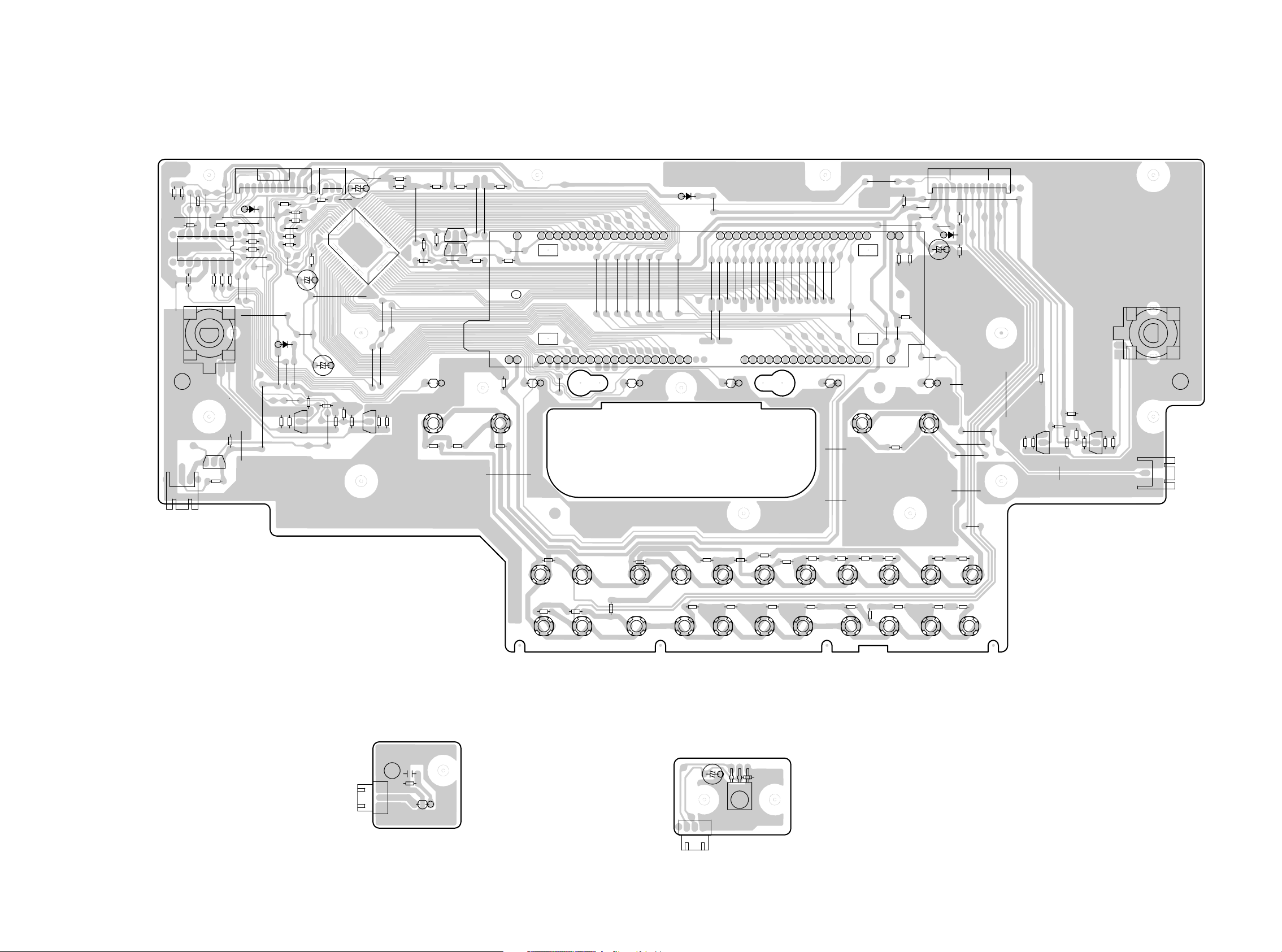
5. PARTS LOCATION (Pattern Side)
SU32
SU33
JU02
DU06 DU04
DU02 DU05DU03
DU01
CU08
RU60
QU06
RU62
QU05
RU59
CU07
RU31
RU17RU18
RU56
QU03
QU07
RU13 RU12
RU11
RU22
RU21
RU01
RU02RU03
RU04
RU05RU06RU07RU08
RU24
RU14
RU15
RU23
RU09
RU29
RU19
RU25
QU04
JU03
CU06
RU54
RU48
JU04
SU01
SU02SU03SU04SU05SU06SU07SU08
SU09
SU10
SU11
SU12
SU13SU14
SU15 SU16 SU17SU18SU19
SU20
SU21
SU22SU23 SU24
SU26SU25
CU05
RU53
RU55
RU61
CU21
DU07
CU23
RU26
RU16
RU27
RU28
RU43
QU09
QU08
CU15
CU16
JU01
CU29
CU10
CU28
CU26
CU09
RU41
CU17
CU24
DU21
DU08
CU22
CU12
RU44
CU11
RU63
QU02
CU02
CU01
RU40
CU14
JU05
RU42
CU20
U101
U102
U103
U104
U105
U106
U107
U108
U109
U110
U111
U112
U113
U114
U115
U117
U118
U119
U120
U121
U151
U152
U153
U154
U155
U156
U157
U158
U159
U160
U201
U202
U203
U204
U205
U206
U207
U208
U209
U210
U212
U211
U251
U252
U253
U254
U255
U256
U257
U258
U259
U260
U261
U262
U263
U264
U265
U266
U267
U268
U269
U270
U301
U302
U303
U304
U305
U351
U352
U354
U355
U356
U357
U358
U359
U360
U353
U361
U401
CU25
U551
RU32
RU33
RU34
RU35
RU36
RU37
U116
DU20
U122
U123
U124
CU27
CU30
CU31
CU04
CU33
CU32
CU03
CU13
CU18
CU19
RU38RU39
RU51
RU52
RU57
RU58
DO
CLK0
STB
LEFT
GND
CLR
CE5
VOL-DW
VOL-UP
5
10
30
35
40
15
45
ATT
AUTODOLBY
BAND
THX
FM-MODE
BASS_-
TREBLE_-
DISP-OFF
MULTI
PRESET
A-TUNING
AUX
DVD
TV
MEMOCLD-COPYT-COPY
STEREO
V-COPY
S-DIRECT
BASS_+
TREBLE_+
PU04
LDVCR1
DSS/V2
1
3
1
3
12.RIGHT
20
50
55
60
65
70
75
80
85
90
9598
WA326J501-0
K-3
K-2
K-1
K-0
FIL-B
1.FIL-A
+5.6VD
+5.6VL
DATA0
11.VKK
WU02
WU01
QU01
ML9205-01GA
1.RST FL
CLK FL
VU01
EXDTS
SURR.
5 STEREO
GND
+5VB
1.R.C
3.DATA FL
NJU3711
A/D
PU04
QU01
QU02
QU81
CU82
CU81
JU81
+
PU84
1
3
WA326J502-0
PU84
QU81
PU74
31 32
WA326J503-0
PU74
CU71
3
RU71
JU71
1
DU71
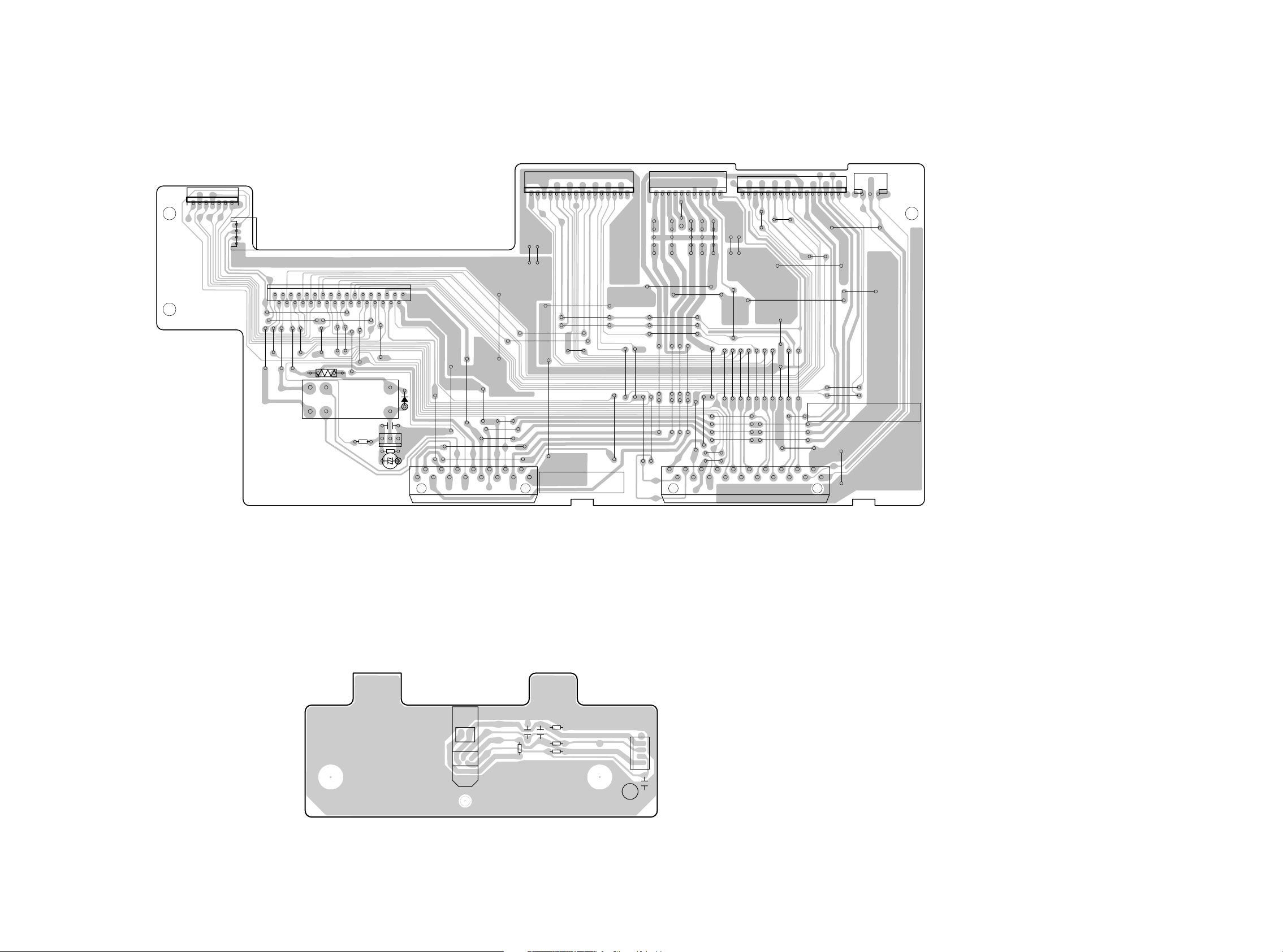
PY64
CLKDISIG
JY70
RY-CMT
R-DO
M-RY
HP-SW
GND
QY61
1
CLK0
DATA0
UY28
UY29
DATA0
161
CLK0
RC-5
UY30
UY51
UY85
T-M
M-RC
JY69
AUX-R
M-M
CDR-M
V1-M
AUX-L
AUX-L
GND
AUX-R
L-OUT
R-OUT
TU-L
TU-R
R-M
-24V
L
R
GND
TU-L
CE
SD
71
P-DO
1
TU-R
CE6
T-M
V-M
M-M
C-M
JY63
CE0
LRG/SML
161 111
RC5
CE3
M-RC
M-RL
JY68
UY82
UY79
15V
24V
RDS-D0
CE2
TU-DI
CE1
TU-SD
CE6
CE3
CE7FLCE0
FL
P-DOWN
RC-5
LRG/SML
S-DET2
DATA0
CLK0
OSD1
S-DET1
OSD2
TU-CE
POWER
MULTI
TU-CLK
TU-DO
VKK
MLT-RC-OUT
GND
PY64
WA300J6010
JY61
UY50
UY17
UY49
UY83
UY48
UY18
UY16
UY15
RY61
LY61
UY14
H.P
UY81
UY13
UY47
RY62
UY41
CY61
RY63
RELAY
UY40
+
QY61
CY62
+5VL
DY61
UY97
UY96
UY95
UY39
UY98
UY99
UY37
UY38
UY94
UY10
UY89
UY12
JY65
+5VB
UY93
+5VA
+3.3V
UY88
UY09
FFVKK
UY77
UY78
24V
P-DOWN
UY75
UY76
UY92
DSP-15V
POWER
-5V
+5VL
-15
+15
MLT-RC-OUT
UY91
UY26
UY90
UY74
UY36
-5G3.3
UY25
UY27
UY68
UY69
UY70
UY73
UY35
+5VD
UY05
UY72
UY34
+5VA
UY24
UY86
UY71
UY33
+15
GA
JY67
UY23
UY67
-15
UY66
UY07
UY08
UY22
UY62
LTGART
UY61
UY04
UY52
UY60
UY43
UY44
UY45
UY46
JY64
UY80
UY59
CE7
OSD-INT
UY58
CE2
UY03
UY57
CE1
OSD-2
UY56
OSD-1
UY01
UY11
UY55
UY63
UY64
UY65
S-DT2
UY32
S-DT1
UY54
UY06
UY31
-24V
JY62
UY21
UY53
+5VV
UY84
+5VL
UY02
GND
D+15V
-15V
+15V
CE0
CE3
PU94
PU94
WA326J507-0
QU91
1
QU91
345
2
6
RU91
CU94
CU91
CU92
RU93
RU92
GND
DOWN
+5VD
JU91
1
UP
4
CU93
33 34
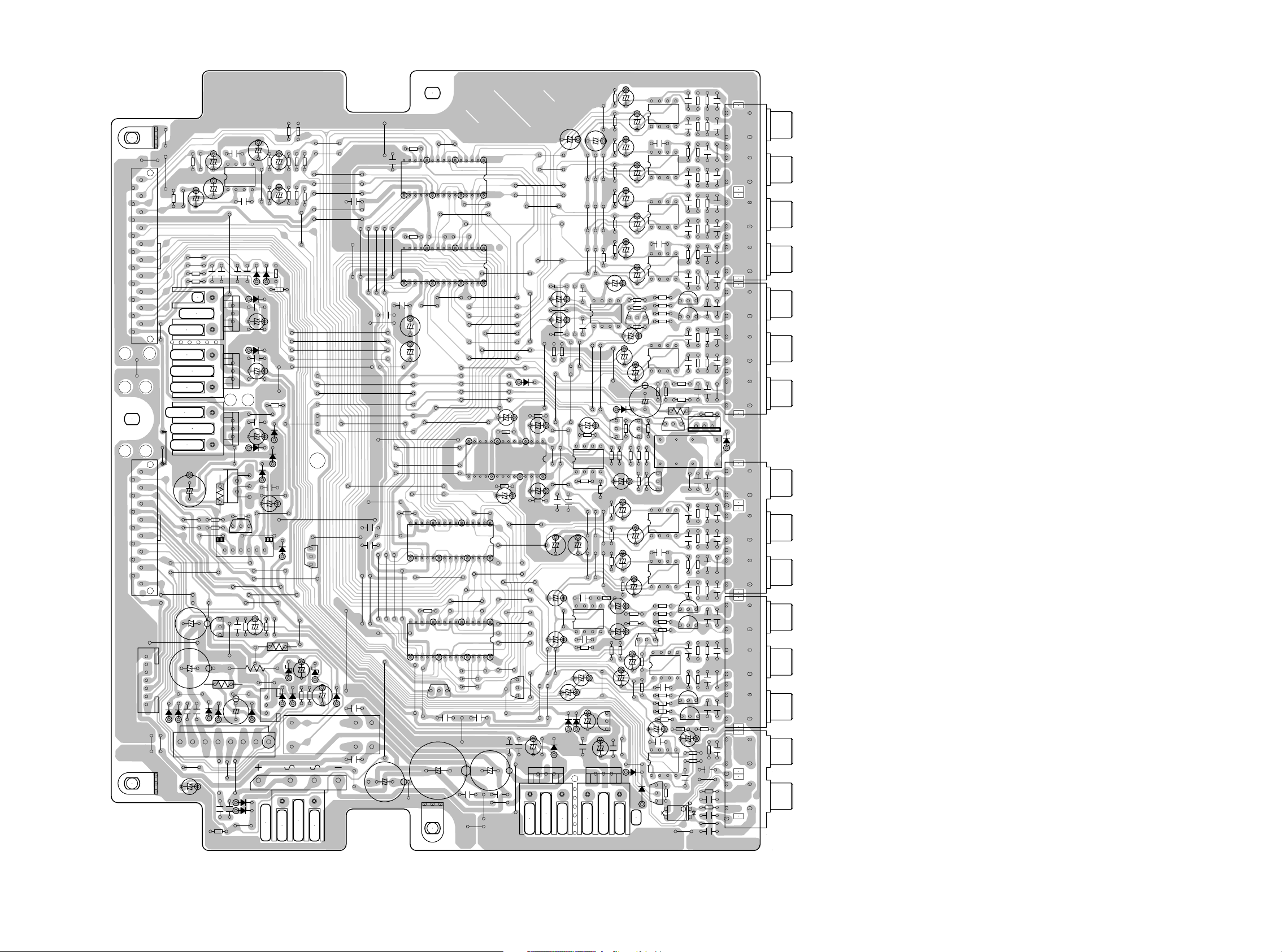
QS11
Q803
Q805
Q804
Q802
Q810
Q813
Q809
PS04
AUX-L
GND
AUX-R
L-OUT
R-OUT
-24V
TU-L
TU-R
R-M
V1-M
M-M
CDR-M
T-M
RCMIN
RC-5
DATA0
CLK0
CE0
CE3
+15VD
-15VD
/GND
RCMOUT
-5V
POWER
+5VL
-15VA
+15VA
+24V
P-DOWN
VKK/-24
+3.3V
+5VD1
+5VD2
+5VD1
+5VD2
+3.3V
24V
F
F
GND
+8V
+8V
+12V
24V(VKK)FF5VGND
GND
J809
20 115 1
US31
5V
J808
CS06
+
CS01
CS26
D826
CS05
CS07
CS09
CS13
CS35
CS27
RG16
CS03
RS64
RS63
+
US06
RS70
RS95
+
+
US02
+
+
+
+
CG09
QG06
RG12
CS02
CS12
CQ10
CS68
RG11
RS25
RS26
+
RS94
RS93
RS80
RS69
RG09
RS84
+
NJM4558DD
NJM4558DD
NJM4558DD
NJM4558DD
QS21
NJM4558DD
RG05
QG05
RG13
NJM4558DD
CS60
NJM4558DD
NJM4558DD
NJM4558DD
QS27
QS04
QS04
QS05
QS05
QS06
QS06
CS74
QS07
QS07
RS72
RS74
RS73
RS71
QS09
QS09
RS56
RG15
QS01
QS01
QS02
QS02
RS62
RS66
RS65
RS61
QS10
QS10
QS25
RS55
QG04
QS25
LG01
CS93
RS79
+
CS11
RQ28
QS26
QS20
QS19
RS90
RS89
LG01
QS17 QS18
QS24
US05
CS66
CS65
CS67
CS70
CS69
CS73
CS80
CS79
CS56
CS55
CS59
CS94
QS23
RS22
RS28
RS18
RS81
RS76
CS99
US01
RS50
RS49
CQ09
CQ08
RS20
RS19
RS08
RS21
RS24
RS23
RS14
RS27
RS88
RS87
CS71
CG07
RS16RS15
RS04
RS17
RS82
RS77
RS83
CS46
CS52
CS53
RG06
CS40
CS41
CS95
CS85
US03
US04
CS88
RS06
RS05
RS07
RS10
RS09
RS13
RS40RS39
CS72
CG08
RS02
RS01
RS03
RS78
CS91
RS75
CS44
CS43
CQ01
CS45
CS48
CS47
CS82
CS51
CS54
CS49 CS50
CQ03 CQ02
CS38
CS37
CS81
CS39
CS42
CS92
CS83
CS96
RQ27
JS01
JS03
QG03
JS04
JS04
JS06
CS84
JS07
R
TV
QS04
L
R
LD
L
JS01
R
QS15
DVD
QS05
QS06
L
R
IN
L
QS14
QS07
VCR1
R
OUT
L
QS08 QS21 QS19
QS20
R
IN
JS03
L
DSS/VCR2
QS09
R
OUT
L
QG04 QG03
QG07 QG06
DG01
QG01 QG02
R
MULTI
QG05
L
R
CD
L
QS13
QS01
R
IN
QS02
L
TAPE
R
OUT
L
R
IN
JS06
L
QS03
QS12
CDR/MD
R
Q812 QS22
OUT
L
REMOTE
RC
QS16
QS11
QS18
QS17
QS10
QS24
QS23
QS25
JS07
MULTI
RC
Q807 Q808
QS27
QS26
PS04
WA300J401-0
RS57
UQ13
UQ74
UQ54
UQ55
US39
UQ11
R816
RS47
RS48
DS01
D804
C812
D806
C816
C815
1
C811
R812
R817
CS15
CS16
RQ26
US36
+
+
RQ25
C810
D825
D812
J804
D803
D822
C809
US77
D813
RS45
RS46
US79
RS58
RS11
UQ09
C833
RS12
US82
D820
UQ06
+
R809
Q813
RS43
RS44
R808
C834
D814
US73
US74
UQ92
L801
L801
UQ46
UQ47
UQ48
UQ49
UQ50
CQ11
UQ05
UQ52
UQ59
UQ58
UQ04
UQ57
RS54
CQ12
UQ51
RS53
US07
QS15
LC78211
QS15
US09 US08
QS14
LC78212
US52
UQ21
UQ80
UQ22
QS14
US56
US11
CS22
CS21
US75
US91
US80
US76
UQ91
CS24
CS23
RS52
+
+
UQ77
UQ67
UQ68
US90
UQ69
QG01
QS13
LC78212
UQ81
UQ82
UQ83
UQ84
UQ76
UQ85
UQ86
UQ87
UQ88
UQ89
UQ66 UQ65
UQ90
CS97
UQ95
CS98
QS13
UQ40
UQ73
UQ72
UQ71
UQ41
UQ42
UQ43
RS51
UQ03
UQ79
QS12
LC78211
QS12
UQ44
UQ02
D815
+
C836
UQ98
Q812
CS20
C821
C835
UQ99
+
+
+
+
US24
C849
J807
US94
US95
US71
US19
US20
C844
UQ64
US70
+
US23
CS19
US16
C823
+
UQ34
UQ35
UQ36
UQ37
RG01
US72
RG02
UQ25
UQ26
UQ27
UQ28
US85
UQ29
UQ30
UQ31
UQ63
CG02
+
QG01
TC9459N
+
CG01
US63
UQ39
UQ70
US18
US69
C845
US22
CG03
US92
US93
US64
US96
US97
US98
QS22
C824
UQ45
UQ96
US25
UQ08
RQ30
JS09
US27
RQ29
CS18
RS96
RS97
RS98
RS99
US26
CS17
CS77
CQ13
+
QS11
+
NJM4558DD
UQ07
QS11
+
CQ14
CQ06
CQ07
UQ75
CS78
CQ05
CQ04
DS02
+
+
US30
-15VD
US28
-15VA
+
US29
+15VD
US78
US33
UQ10
C851
JS10
C842
1.+24V
UQ15
+12V
GND
US34
US35
-24V
+15VA
UQ53
US81
+15VREF
J803
UQ78
R810
R811
R814
US38
+15VREF
Q802
1
US32
C841
Q804 Q805 Q803
+
C813
C840
C814
D805
D821
+
R815
Q810
UQ12
UQ14
+
R806
D819
R807
C843
US40
C819
UQ16
UQ17
R818
UQ93
+
D828
D829
RELAY
+24V
J805
GND
D808
+
US37
1
D811
1
UQ56
C832
Q809
+
R804
US83
J806
C827
D818
C828
D817
7
UQ94
US42
D816
8
US41
UQ18
C852
C820
R819
DG02
US89
UQ38
C826
+
CS87
US47
US48
UQ19
UQ20
US84
US55
RS68
+
CS34
US10
UQ24
CS33
RG04
+
CG04
+
RG03
CS29
UQ62
+
+
+
CS58
CS30
US67
RS67
RS92
UQ33
CS64
US12
US15
US66
US14
+
RS91
US17
US13
CS63
CS57
UQ23
US58
UQ32
+
NJM4558DD
RG17
+
CS62
NJM4558DD
CS90
+
US68
+
CS89
UQ01
US99
D823
C825
US21
+
D810
D824
-5V
CS76CS75
US57
RS59
C848
+
CG06
RG18
QG02
QS03
C850
+5VL
CS86
US46
US51
US54
UQ61
QG02
US60
US62
+
C830
US43
US45
US44
US50
US49
RS41
US53
+
QS08
NJM4558DD
QS08
UQ60
+
RG19
US87
US59
RS32
US61
US88
RS60
+
+
CS61
RS85
US65
+
Q808Q807
RS34
RS33
RS36
RS35
RS38
RS37
RS42
CS36
US86
QG07
RG20
RS30
RS29
CS32
CS31
QS03
CS25
Q811
D827
+
+
CS08
CS10
+
CS14
+
+
CS28
DG03
RG10
RG14
CG05
+
CS04
+
RS31
QS16
RS86
+
C847
35 36

C801
C802
C803
C804
C806
C807
C808
D801
Q801
Q806
F801
F802
U801
U802
D802
D807
C817
C818
C805
J801
J802
R801
R802
R813
U803
E
B
C
IN
OUT
P804
+12V
+20V
GND
-20V
+15V
REF
+
+
+
+
+
+
1
6
1
4
2A 250V
WA326J506-0
P804
Q801
Q806
PL04
JL10
U245
CL0
DAO
+15
-15
GND
5VL
5VV
-24V
S-D1
S-D2
OSD-1
OSD-2
CE1
CE2
CE7
OSD
U158
16
1
2
3
4
5
B
A
B
C
U183
A
B
V-MUT
DVD
PAL
GND
AUX
JL09
1
+
CL64
CL65
U192
U193
B2
DL22
U194
U137
A2
U162
U197
RC95
RC96
JC71
U132
U227
U244
U106
DL21
CL35
U118
U128
RC97
CC95
U161
_KILL
SL6
GND
SR6
C6
GND
SW6
FR
GND
FL
SWA
VCLK
VD ATA
OSD-OUT
CLK0
DATA 0
LL02
+
RL39
U117
U180
U181
U182
U190
U191
U156
U129
QC95
CC64
+
+
+
+
CC86
CC85
RC91
RL23
RL22
QL16
U177
+
CL52
+
U178
CL63
JL13
CL85
RL24
RL18
CL44
QL09
U105
U179
QL10
QL07
U157
NJU3718L
U154
U155
CL80
LL01
CL50
CL49
CL77
U153
RL15
U224
LC74781
U208
CL76
QL09
U207
RL40
U206
U205
U225
U226
RL29
QL18
74HC132
CL51
U116
QL11
QL18
+
CC65
U210
CC72
RC72
RC71
CC76
RC73
U138
RC94
RC92
RC93
NJM4580 NJM4580
RC89
RC90
CC83
CVBS
U133
CC88
JL14
CC71
+
U139
RC74
NJM4580
+
CC73
CC87
CC84
CC74
RC88
RC87
RL26
DL07
CL68
CL55
+
XL02
CL46
14.3MHZ
U243
U151
CL78
U152
+
CL99
RC76
CC75
U211
QC71
RC75
CC77
U196
U237
PL04
+
CL67
QL12
U242
U127
QL19
U126
U238
RC78
RC77
RC79
CC82
RL20
CL16
CL86
RL21
RL28
RL41
QC72QC73
CL53
RL42
+
RC80
+
CL48
U232
U189
CL79
CC78
U231
CL82
U149
U223
U241
COPY
+
QL21
CC81
RC81
CL54
RL19
+
CL36
QL15
+
RL25
QL17
CL15
NJM2244
+
QL08
U147
+
CL75
+
U204
U203
U115
QL06
BA7613N
CL72
CL31
CL40
DL13
U187
U148
CL57
+
CL45
QL04
+
+
CL38
CL98
U222
U125
RL54
RL52
RL51
U195
U130
RC84
RC82
RC83
RC85
RC86
CC79
U131
U160
U146
RL43
CL47
17.7MHZ
B1
CL41
U150
RL53
CC80
RL31
XL01
U188
MULTI
BA7613N
WA326J201-2
37 38
CL69
CL43
+
CL23
U202
+
CL22
U236
+
CL42
U176
DL06
QL02
BA7613N
U103
RL30
A1
CL70
U145
U124
+
U209
U235
CL21
U104
CL25
CL39
CL30
+
U234
U174
U102
CL20
+
+
CL12
+
CL34
CL81
U201
U144
U175
+
+
CL13
U114
+
CL11
+
QL05
COPY
BA7649A
CL56
+
+
+
CL29
+
CL28
U121
U122
U123
+
CL17
MULTI
BA7649A
QL03
+
CL37
U140
U249
CC59
RC69
+
RC70
+
CC60
CC53
RC59
+
RC60
+
CC54
U113
CL18
CL26
U248
CL07
+
U173
U159
U233
+
U112
U246U247
U142
+
U135
U111
U136
CC61
CC62
CC55
CC56
CL08
U184
U185
U186
+
U101
CL27
U143
CL19
+
+
U110
CL09
U141
+
CL58
CL71
U109
+
RC67
QC52
RC57
CL83
+
RL32
U108
U221
+
NJM2244
QL14
+
NJM2114
RC68
NJM2114
QC51
RC58
DL05
CL59
DL03
CL14
CL32
CL73
U171
RL04
CL02
CL03
+
CL33
+
U172
CL74
RL08
U119
+
CL01
+
U107
+
+
+
CL24
RL02
RL06
DL04
RL10
CL05
U120
CL60
+
RL11
RC65
RC66
RC55
RC56
DL01
CL61
RC63
RC64
RC53
RC54
RC61
RC62
RC51
RC52
DL02
CL06
RL14
CC57
CC58
CC51
CC52
RL01
RL03
RL05
RL09
RL13
DL12
CL62
RL12
DL11
U134
DL08
DL10
RL07
JL01
DL09
JL02
JL03
CC63
JC51
TV
LD
DVD
IN
VCR1
OUT
IN
DSS
OUT
MON
OUT
MLT
OUT
C
SW
S-L
S-R
QL16
QL02
QL09 QL15 QL17
QL08
QL10
QL11 QL12
QL07 QL06 QL05
QL14
QL19 QL04 QL03
QC95 QL18
QL21
QC71
QV52
QC73 QC72
QV51

PZ04
JZ06
16
CL0
DAO
+15
-15
GND
U372
5VL
5VV
U373
AX-CV
1
+15
GND
-15
GND
GND
1
16
JZ07
Y
C
U343
U391
-24V
S-D1
S-D2
OSD-1
OSD-2
CE1
CE2
CE7
OSD-
INT
1
2
3
4
5
B
A
B
C
A
B
V-MUT
DVD
PAL
GND
AUX-CV
U387
8
JZ08
1
DZ22
CZ98
LZ02
U390
RX11
U429
U434
RX29
U452
U341
U342
CX06
+
U340
CX05
U451
U350
U329
U330
U339
U446
RZ57
U389
U328
DX01
RZ59
RX02
U438
U445
U327
U278
U447
U282
DZ05
RZ56
U388
+
RX01
WA326J202-2
S-VIDEO
PZ04
U281
DZ21
U326
QZ26
CX01
U275
U276
U277
U280
+
U415
QX01
U371
U325
RX04
U319
U320
U321
U322
U297
U279
RX03
U324
LX01
CX97
CX12
QZ08
U323
U338
RZ58
CX92
CX02
U353
RZ20
QX05
JZ01
RZ72
RZ01
U311
U392
CZ01
U251
RZ02
RZ03
U260
RZ04
CZ04
U264
U262
RZ05
U267
+
CZ55
U331
CX33
U252
CZ83
U332
CZ61
CZ59
RZ35
U285
U286
+
+
+
+
+
CZ87
RZ63
+
+
+
RZ62
RZ17
CZ58
CZ56
CZ57
CZ60
RZ10
RZ11
RZ15
CZ07
RZ08
RZ12
RZ06
+
+
RZ18
CX31
+
RZ31
CX32
+
+
+
+
U431
RZ16
RZ34
RZ32
RZ24
RZ26
RZ13
RZ61
RZ27
RZ25
RZ28
CZ06
RZ07
RZ73
RZ09
CZ08
CZ09
RZ75
RZ19
CZ82
RZ74
JZ02
U408
U430
RZ30
U412
RX31
RX33
RZ29
RZ76
V2
RX32
C
TV
Y
C
LD
Y
C
DVD
Y
C
IN
Y
C
OUT VCR1
Y
C
IN
Y
DSS/
C
OUT
Y
C
MONI
Y
Y
JZ03
RX20
RX17
RX18
U283
U284
RX19
RX21
U344
QZ07 QZ04
QZ08
QZ02
QZ21
QZ05
QZ06
QZ20
QZ26
QZ19
QZ11
QZ10
QZ22
QZ12 QZ13 QZ14 QZ09
PW54
QW52
QW53
QW54 QW51
QZ28
QX02
QZ19
QX03 QZ24
QX01 QX05 QX04 QZ25
QZ29
QX07 QX27 QZ16
QZ17
QZ18
+
CX25
LZ03
CZ36
CZ35
+
U407
CZ52
CX03
U273
+
U406
CZ33
CX99
U296
RX08
RX25
CZ39
+
COPY-C
CZ27
++
U271
COPY-Y
U272
CZ34
+
+
QZ06
COPY-Y
CZ51
+
CZ50
CZ44
14.3MHZ
RZ54
QZ14
U394
QX02
RX06
RX07
QZ29
QZ29
74HC132
RX26
RX27
CX21
+
COPY-C
CZ40
+
CZ28
17.7MHZ
CZ45
CX98
RX28
+
QX03
+
CX20
CZ75
U317
U318
QZ07
U259
CZ41
U258
+
+
CX46
+
CZ42
U428
+
CX10
U386
U274
CZ73
CX45
U433
CZ49
CZ48
+
QZ11
LC74781
LZ01
CZ43
CZ47
CZ46
XZ02
QZ12
QZ13
CX08
U395
RX05
RX10
QX04
U304
CX22
U257
++
QZ05
+
+
CX04
RX09
RX24
U256
U426
+
CZ37
U305
CZ38
U427
U404
QZ02
CZ70
U405
U396
CZ32
RX12
U444
U443
CZ81
+
DZ02
CX15
++
DZ01
U347
RZ67
U348
XZ01
U385
+
U294
U295
+
CX24
U349
U413
+
CX07
U302
U303
QX07
U425
+
CX14
CZ80
U370
U270
CX13
U414
RZ53
RX16
QZ27
U424
U369
CZ72
+
U293
CX44
U255
CZ23
+
QZ21
U378
U336
U337
U379
U380
CZ88
NJM2263
QZ10
U432
CZ97
QZ24
DZ03
CZ78
U368
QZ04
INPUT-C
U423
+
CZ22
+
CZ29
CZ30
+
U269
U377
+
CZ31
RX15
NJM2244
QZ09
+
U422
+
RZ50
JZ10
+
CZ24
U313
CX43
U367
CZ25
U314
CZ21
+
CX09
+
U374
CZ26
+
U411
U335
CX11
+
U375
U376
CZ15
U442
+
CZ19
+
U315
U366
U316
CZ86
++
+
U441
+
U409
CZ17
+
CZ14
U334
QZ20
NJM2263
RX13
U333
CZ13
CX41
U363
+
CZ12
CZ16
CZ11
RX14
+
CX48
NJM2244
CZ18
CZ20
+
CZ84
U410
QZ19
CZ92
+
CZ66
RZ60
U292
NJM2903
QZ23
QZ25
RZ52
+
CX16
RZ47
U352
JZ09
CZ89
RZ44
DZ19
U437
U301
CZ67
U291
U345
U290
U381
U382
U384
U383
U346
CX19
CX17
U351
QZ16
QZ18
U289
QZ17
U288
CZ74
RZ42
RZ43
CZ76
RZ45
+
RZ51
CZ90
CZ91
CZ65
CZ68
RZ46
RZ48
CZ77
U393
U362
+
CZ69
CZ71
U312
CZ93
QZ28
U448
U298
U299
U300
CX42
U365
U265
CX49
CX47
CX18
QZ28
74HC32
U436
U254
U364
U266
CZ94
+
74HC4051
74HC4051
+
CZ62
+
U453
U454
CZ02
U421
U261
U263
RZ65
RZ14
U268
CZ95
+
RX22
QZ22
QZ22
U287
CZ63
CZ85
U253
U361
U402
CZ10
CZ05
U401
+
+
+
CZ03
+
+
+
+
+
U435
39 40

P104
QA03
Q202
Q205 Q203
QA02 QA01
Q501
Q202
Q204
Q354
QA06 - QA04
Q353 - Q351
Q301
QM13 - QM11 - QM09
QM17
QM15 QG53
QV11
QV10
QV20 - QV13
QV09
QG51
QV03
QV02
41 42
QG52
QV07
QV06
QV01
QV05
QC03
QC01
QC07 QC08

P704
CT01
CT25 CT23
CT03
CT07
RT05
+
RT03
RT01
RT85
QT03 QT01
QT09 QT13
QT19 QT23
RT37
CT05
+
RT11
RT39
CT17
RT89
LT01
RT83
U057
C-CH
QT03
QT01
U076
QT09
U075
QT13
IDL
RT43
RT47
CT09
U072
U071
U063
U061
RT73
DT19
DT15
RT59
RT55
QT19
CT29
RT65
QT23
RT71
51
U067
RT09
RT07
RT29
RT33
RT31
U074
RT45
RT51
U060
U058
RT67
U070
U065
CT15
RT41
J705
RT19
DC
RT15
RT17
RT23
U073
IDL.TP
+
-
JT13
41
DT05
+
DT07
DT11
DT09
RT63
RT61
RT69
QT07
QT11 QT05
QT17 QT21 QT29
51
POSIST
NC
J704
C.DET
L.OUT
3MIX
RT27
RT35
QT05
RT13
DT01
R788
U069
RT49
U064
U062
RT57
QT29
CT21
+
U068
U066
71
FL-CH SR-CH C-CH
U059
RT75
RT77
U056
RT81
U055
J711
DT21
QT17
QT11
DT17
CT27
CT19
QT07
RT25
RT21
DT03
+
CT11
DT13
+
CT13
RT79
RT53
QT21
Q704 Q702
Q710 Q714
Q720 Q724
51
J717
-B
U029
R790
R712
R740
R760
J716
TEMP
3131
SW.
+24V
+24V
R748
C710
-B
U033
C724
Q720
Q724
SW.
Q704
U052 U051
Q702
Q710
Q714
IDL
R744
U048
U047
G
U046
+B
U044 U042
U041 U040
U039
U036
R774
D716
D720
R756
C730
R766
R772
J701
U078
U077
GNDSRGND
FL
C
R738
U053
U082
R787
RT87
R786
J702
61
C706
+
C708
C718
C704
R706
R704
+
C702
R702
GND
J703
+B
31
-B
L702 L701
R784
U026
U028
U027
C726
U023
U022
-B
J706
Q708
Q712 Q706
Q718 Q722 Q730
TEMP
SR-CH
U083
J714
D708
D706
R724
U049
IDL.TP
R716
U043
+
R764
R770
DC
C728
U038
Q718
D718
Q722
J707
R762
R722
D704
D714
Q708
R726
Q712
Q706
+
+
C712
C714
U037
U035 U034
R754
U031
R758
U025
U020
+B
R710
R708
R730
R734
R732
U050
R752
U032
C716
R746
U021
+
R720
R718
-
41
+
D712
D710
R742
R768
C720
61
U030
U024
U019
R736
D702
R728
R714
R776
Q730
C722
+B
R782
D722
U054
WA300J1022
U084
R737
+
C707
C703
R705
+
R750
C701
R703
R701
U045
R780
U081
C725
R785
R778
U017
U018
C723
D721
Q729
C721
U003
R779
5151
J708
Q703 Q701
Q709 Q713
Q728 Q719
Q703
Q701
C705
Q709
R711
Q713
R739
C717
R747
C709
R789
U006
R783
R755
R777
Q719
R781
R771
U002
C729
Q723
P704
U016
U015
IDL
R743
U013
U009
U008
D715
R759
R765
+
J710
U012
J715
TEMP
OUT
FL-CH
R719
R709
R707
R729
R733
R731
U079
R751
U011
U010
R773
D719
R745
C719
R715
R717
R723
U014
+
IDL.TP
-
J713
41
D717
U005
D707
C715
+
D709
D711
R741
R761
U001
R767
J709
Q707
Q711 Q705
Q717 Q721
31
+24V
Q707
DC
R725
Q711
R721
D703
+
C713
C711
+
D713
U007
R753
R757
D705
C727
Q717
Q721
R763
R769
J712
Q705
R749
R775
R727
R735
R713
D701
P774 P794
J785
J784
J783 J782 J781
WA300J1032
P774
U756
U755
U754
U753
U746
U748
U745
U744
Q726
U747
U743
2SC2922
Q726
U742
U778
U777
U776
U774
U773
U772
U771
U775
2SC2922
Q725
U770
U769
2SC3419
Q715
U762
Q725 Q715 Q727
U761
U764
U760
U759
U763
U766
U765
U758
U768
U767
U757
2SA1216
Q727
43 44
U741
U752
U751
U750
U749
2SC3419
Q716
Q716
U740
U739
U738
U737
U726
U733
U725
P794
D799
U736
U735
U734
WA300J1042
U729
U728
U727
2SA1216
Q728
U732
U731
U730
Q728 QT25
U724
U723
U720
U719
U716
U722
U721
U715
U718
U714
U717
U713
2SC2922
QT25
U712
U711
5161615151
U710
U709
U707
U708
2SC3419
QT15
U706
U705
U704
U703
QT15 QT27
U702
2SA1216
QT27
U701

P754
PT04
RED BLK BLK
RED
SL-GND
FL-GND
SR-GND
FR-GND
6
1
3
1
7
1
5
1
JN55
JN54
PT04
WA300J6030
SL SR
FL FR
UT53
UT52
UT51
UT15
UT14
UT13
UT12
UT11
UT10
UT09
UT08
UT07
UT06
JN56
JN53
JN52
JN51
CN58
CN57
CN56
CN55
CN54
CN53
CN52CN51
DN52
DN51
UT21
DN53
UT23
UT24
UT28
UT29
UT34
UT33
UT32
UT30
UT31
UT43
UT42
UT27
UT26
UT25
UT22
UT05
UT04
UT03
UT02
UT01
UT41
LN53
LN52
LN51
QN13
QN14
QN03
QN05 QN04 QN06
QN02 QN10 QN12 QN11
QN09 QN08 QN07
JP06
CN16
QN13
RN41
RN40
RN42
31
JN09
CN13
C872
+
UN13
RN38
UN09
D871
J871
CN09
+
GNDSTOP DC
RN05
+
CN03
CN04
+
C871
UN12
UN08
UN07
Q871 Q861
41
HP.L
JN08
HP.G
HP.R
MODE
DN03
UN24
UN23
RN43
QN14
RN10
RN13
RN09
QN01
RN07
RN11
+
CN06
CN05
+
RN49
+
C861
D861
UN05
UN06
C862
CN08
+
UN11
QN03
+
+
CN01
RN01
UN04
RN45
41
LN01
UN21
RN16
RN15
RN17
QN05
DN10
CN10
RN48
RN14
QN04
QN02
RN08
RN06
CN07
UN19
CN02
RN04
DN01
DN02
71
RN12
UN18
RN20
QN10 QN09 QN08
RN25
CN12
RN35
RN34
RN29
RN33
RN23
RN24
+
CN17
RN22
DN04
RN21
CN11
+
UN17
UN10
D881
UN03
UN02
Q881
UN01
D882
R881
Q871 Q861 Q881 QP28
NC
+
+
C882
RN18
RN32
RN30
RN28
RN27
C881
RLY.
DN07
QN12
QN11
RN46
RN19
RN37
RN36
UN16
HPSW
UN26
RN31
QN06
UN20
CN15
MUTE
DN05
RN26
DN06
JN03
UN25
UN15
UP59
CN14
CP26
UN14
UP58
CP02
QN07
UP57
CP08
CP04
RP86
CP24
2SA1216
QP28
UP56
RP38
CP06
+
RP06
+
RP04
RP02
LP02
RP84
UP86
UP62
CP30
UP61
UP55
UP54
QP20 QP24
QP04 QP02
QP10 QP14
QP04
QP02
QP10
RP12
QP14
RP40
CP18
RP90
UP75
QP20
QP24
UP65
RP72
RP48
CP10
RP66
RP60
IDL
UP79
UP66
DP16
RP56
UP52
QP16 QP26
UP83
UP82
RP44
UP51
UP70
UP60
RP68
UP78
RP74
DP20
RP46
UP77
UP50
UP74
UP72
RP10
RP08
RP30
RP34
RP32
UP80
RP52
UP64
CP16
RP42
2SC3419
QP16
QP08
QP12 QP06
51
RP16
+
DP12
+
FR-CH
RP20
RP18
RP24
DC
UP81
DP18
DP06
DP10
RP64
RP62
CP20
RP26
DP08
RP70
UP49
RP54
CP28
UP76
QP08
DP14
UP48
RP22
+
UP47
QP12
CP12
RP58
QP22
UP73
QP18
UP46
RP28
RP36
DP04
+
CP14
UP71
UP69
UP68
2SC2922
QP26
UP45
QP06
UP63
UP44
RN44
RP14
DP02
RP78
CP22
DP22
RP50
JN02
RP76
QP30
UP43
UP42
UP41
+
-
IDL.TP
JP04
41
UP39
JN10
LOCK
SPEED
T-2CH
PO-DWN
GND
-B
+B
UP30
41
1
UP67
RP82
JN05
6
RN02
DN09
+B
RLY
UP27
FR-CHSL-CH
RN03
RP80
JP01
31
FR
UP38
41
FAN.TP
T-3CH
UP32
UP28
RP83
RP85
UP26
2SA1216
QP27
GND
CP01
UP16
JN04
3MIX
RP37
SL
+
CP07
CP03
RP05
RP03
+
RP01
LP01
CP25
CP23
UP18
UP15
UP14
UP13
QP18 QP22 QP30 QP19 QP23
QP27 QP15
QP03 QP01
QP09 QP13
POSIST
NC
L.OUT
C.DET
RP11
QP01
CP05
RP39
CP17
RP47
CP09
RP89
UP21
UP19
CP29
RP71
UP12
UP11
P754
WA300J1012
QP03
UP40
RP09
RP07
RP15
UP34
RP55
UP25
IDL
UP37
RP43
UP33
UP29
UP23
UP31
DP15
UP09
RP73
DP19
RP29
RP33
RP31
UP36
RP45
UP17
UP08
RP51
RP67
CP15
UP07
UP20
+
RP41
2SC3419
QP15
DP11
CP19
QP19
QP23
QP09
QP13
RP59
RP65
RP19
RP17
DC
RP23
RP21
DP05
DP09
RP63
+
QP07
QP11 QP05
SL-CH
QP07
QP05
RP25
QP11
UP35
+
+
CP11
CP13
DP17
DP13
RP53
RP57
DP07
CP27
QP17
QP21
RP61
RP69
UP06
UP05
UP04
RP27
RP35
RP13
DP01
DP03
UP24
UP22
2SC2922
QP25
UP03
RP49
UP02
JP05
JP03
41
-
RP75
UP01
RP79
+
QP29
RP81
IDL.TP
DP21
RP77
CP21
45 46

CL80 CL79
CL92
CL93
CL91
CL82
CL81
UL71
CL96
CL95
CL94
CL88
CL84
CL97
CL98
JL76
CL83
JL77
JL75
RL85
RL94
RL86
RL92
RL93
RL89
RL88
RL90
RL91
CL75
RL75
RL77
CL90
RL78
RL76
CL76
CL77
RL79
RL81
CL78
RL80
RL82
RL84 RL83
RL87
CL89
QL75
LR
PL74
WG300J102-0
WL75
GND
Y
GND
CV
-15V
GND
1
++
+
+
+
+
7.+15VB
1.C
+
PL74
QL75
CW03
JW02
JW01
CW02
CW01
PW04
WG300J103-0
WW01
PW04
CY03
QY01
QY02
QY03
QY04
QY05
QY06
QY07
QY08
JY01
JY02
JY03
JY04
JY05
JY06
QY09QY10
QY11
QY12
QY13
QY14
XY01
CY02
CY29
CY30
CY23
CY22
CY21
CY20
CY25
RY14
RY16
RY22
RY18
RY20
RY21
RY19
RY23
RY17
RY15
RY52
CY17
CY18
CY19
CY26
CY27
CY09
CY28
CY24
RY25
RY24
RY13CY08
CY07
CY06
CY05CY04
RY11
RY12
RY09
RY10
RY67
RY08
RY07
RY04
RY05
RY03
RY02
RY66
RY69
CY01
RY01
RY57
RY59
RY60
RY58
RY64
RY68
RY65
RY32
RY33
RY34
RY35
RY36
RY38
RY37
RY45
RY44
RY43
RY42
RY40
RY41
RY39
CY16
CY15
RY56
RY55
RY54
CY14
RY53
CY13
CY12
RY48
RY47
RY49
RY50
RY51
RY46
RY30
RY29
RY27
RY28
CY10
RY31
CY11
RY06
DY01
DY02
QY15DY0 4
DY0 3
FLFL+5VD
STB
DI-FL
KEY1
KEY2
KEY3
KEY4
+5VB
LEFT
RIGHT
1
11
IR
VOL-UP
VOL-DOWN
DATA 0
CLK0
CE5
CLR
GND
GND
+5VL
VKK
19
GND
GND
DO
DI
RST
CLK
REQ
ACK
MUT
GND
UP
DOWN
FL
CE0
CE7
CE3
RDS-DI
CE6
TU-DI
TU-SD
CE2
LRG/SML
RC-5
P-DOWN
DATA 0
S-DET2
CLK0
H.P.
S-DET1
OSD2
POWER
TU-CE
RELAY
TU-CLK
MULTI
TU-DO
POW-DET
+5VL
GND
10-CE1
20-OSD1
30-VKK
112
+
+
PY04
+5VD
24V-DET
1
4
1-FL
RST
MLTRCOUT
123456
CDEF
123456
789
10 11 12
BA
0123
01234
0
1234
+
+
++
+15V
+24V
RST GND
WG300J101-2
+
PY04
QY02 - QY08
QY01
QY11 QY12
QY13 QY14
QY15 QY10 QY09
P854
JB71
CB71
SB71
PB74
1
WA326J505-0
PB74
J851
R852
D854
C852
U814
U813
31
U815
C851
D853
R851
C857
+
R853
+
U822
D851
R854
J856
WA300J6020
P854
+
U821
+
J855
U811
U812
C853
+
J853
J854
5
1
1
1
J852
4
3
PB04 QB01 QB02
UB02
1.TEMPOUT
2.
3.24V
JB04
3.+24V
2.GND
1.RELAY
12A 250V
QB01
FB01
PB04
WA300J402-0
QB02
CB02
JB12
+
RB03
RB04
JB01
CB03
JB02
RB02
1
JB05
1
JB06
1
JB09
630mA 250V
JB10 JB11
UB01
FB02
RB05
UB07
UB06
LB03
CB01
1
JB08
LB02
PB54 QB51 QB52
DB01DB02
1.TEMPOUT
3.24V
UB52
2.
UB03
UB04
JB03
UB05
JB54
3.+24V
2.GND
1.RELAY
QB51
T6.3A 250V
1
RB01
1
JB59
47 48
JB07
PB54
WA300J403-0
JB62
RB53
JB51
FB51
JB52
JB55
CB52
CB53
QB52
RB54
1
JB56
JB60
UB55
UB56
RB52
FB52
T315mA 250V
RB55
UB57
JB61
LB53
UB51
CB51
DB51DB52
LB52
UB53
JB53
UB54
1
JB58
JB57

P604
QK05
QK03
QK01
QK06
QK04
QJ01 QJ02
QD03
QH53
QJ71
QD42
QH52
QH51
QD02
QH03
QJ51
QD41
QH02
QH01
QD01
QE01 -
QR07
QE08 QE01
QE04 - QE07
QR03 QR02
QE10
QE09
QR05
QR04
Q604
QR01
Q601
QR06
Q652 Q653
Q603 Q602
Q651
QD43
Q694
49 50
Q693 Q692Q605QR10 QR09
Q691

6. IC DATA
SERIAL
DATA
INTERFACE
8 x F
S
INTERPOLATOR
SERIAL CONTROL
INTERFACE
AUTO-CLOCK
DIVIDE CIRCUIT
VOLUME
MUTE
CONTROL DATA
INPUT
3
2
DIGITAL
SUPPLY
CLOCK
IN
ANALOG
OUTPUTS
22
ZERO
FLAG
ANALOG
SUPPLY
DE-EMPHASISMUTE
RESET
2
SERIAL
MODE
16-/18-/20-/24-BIT
DIGITAL
DATA INPUT
AD1852
MULTIBIT SIGMA-
DELTA MODULATOR
ATTEN/
MUTE
DAC
MULTIBIT SIGMA-
DELTA MODULATOR
8 x F
S
INTERPOLATION
ATTEN/
MUTE
VOLTAGE
REFERENCE
DAC
Pin In/Out Pin Name Description
1 I DGND Digital Ground.
2 I MCLK Master Clock Input. Connect to an external clock source at either 256 F
S
, 384 FS,
512 F
S
, 768 FS, or 1024 FS.
3 I CLATCH L atch Input for Control Data. This input is rising-edge sensitive.
4 I CCLK Control Clock Input for Control Data. Control input data must be valid on the rising
edge of CCLK. CCLK may be continuous or gated.
5 I CDATA Serial Control Input, MSB first, containing 16 bits of unsigned data per channel. Used
for specifying channel-specific attenuation and mute.
6 N C N o Connect.
7 I 192/48 Selects 48 kHz (LO) or 192 kHz Sample Frequency.
8 O ZEROR Right Channel Zero Flag Output. This pin goes HI when Right Channel has no signal
input for more than 1024 LR Clock Cycles.
9 I DEEMP De-Emphasis. Digital de-emphasis is enabled when this input signal is HI. This is used
to impose a 50µs/15µs response characteristic on the output audio spectrum at an
assumed 44.1 kHz sample rate. Curves for 32 kHz and 48 kHz sample rates may be
selected via SPI control register.
10 I 96/48 Selects 48 kHz (LO) or 96 kHz Sample Frequency.
11, 15 I AGND Analog Ground.
12 O OUTR+ Right Channel Positive Line Level Analog Output.
13 O OUTRÐ Right Channel Negative Line Level Analog Output.
14 O FILTR Voltage Reference Filter Capacitor Connection. Bypass and decouple the voltage refer-
ence with parallel 10µ F and 0.1µ F capacitors to the AGND.
16 O OUTLÐ Left Channel Negative Line Level Analog Output.
17 O OUTL+ Left Channel Positive Line Level Analog Output.
18 I AVDD Analog Power Supply. Connect to Analog 5 V Supply.
19 FILTB Filter Capacitor Connection. Connect 10µ F capacitor to AGND (Pin 15).
20 I I DPM1 Input Serial Data Port Mode Control One. With IDPM0, defines 1 of 4 serial modes.
21 I I DPM0 Input Serial Data Port Mode Control Zero. With IDPM1, defines 1 of 4 serial modes.
22 O ZEROL Left Channel Zero Flag Output. This pin goes HI when Left Channel has no signal
input for more than 1024 LR Clock Cycles.
23 I MUTE Mute. Assert HI to mute both stereo analog outputs. Deassert LO for normal operation.
24 I RESET Reset. The AD1852 is reset on the rising edge of this signal. The serial control port
registers are reset to the default values. Connect HI for normal operation.
25 I L /RCLK Left/ Right Clock Input for Input Data. Must run continuously.
26 I BCLK Bit Clock Input for Input Data. Need not run continuously; may be gated or used in a
burst fashion.
27 I SDATA Serial Input, MSB first, containing two channels of 16, 18, 20, and 24 bits of twos
complement data per channel.
28 I DVDD Digital Power Supply Connect to digital 5 V supply.
Table I. Serial Data Input Mode
IDPM1 (Pin 20) IDPM0 (Pin 21) Serial Data Input Format
0 0 Right-Justified
01I
2
S-Compatible
1 0 Left-Justified
11DSP
QE09:PM4007A
QPSK input
LPF
VCXO
18.432 MHz
CPIN
CMIN
DOUT
DOUTB
PDDIS
PDO
QD01-QD03,QD41-QD43:AD1855
SYNC
9KHz
DetectionSafeguard
Demoduration
46.08MHz
oscillator
46.08MHz
Phase
comparator
VI
VO
1/2048
divider
1/2
Timing
S/P
9.216KHz
DAI
control
Address
Error
correction
A (14:0)
DB(7:0)
OEB
WEB
C2F1
C2F0
C1F1
C1F0
MUTO
SRAM
32K x 8
RESET
No. Name I/O Function
1 GND - GND
2 VDD - +5VD
3 RESET I System Reset At “L” reset
4 OSCON I Oscillator control
5 DATA I TEST
6 MCK I TEST
7 MLTB I TEST
8 IDST O TEST
9 IDCK O TEST
10 IDO O TEST
11 TM0 I TEST
12 ECCK O TEST
13 DEN O TEST
14 DRY O TEST
15 MSYC O TEST
16 TM1 I TEST
17 A0 O RAM A0
18 A1 O RAM A1
19 A2 O RAM A2
20 A3 O RAM A3
21 A4 O RAM A4
22 A5 O RAM A5
23 TM2 I TEST
24 TM3 I TEST
25 XOUT O TEST
26 XIN I TEST
27 XEXT I TEST
28 GND - GND
29 VDD - +5VD
30 A6 O RAM A6
31 A7 O RAM A7
32 GND - GND
33 VDD - +5VD
34 A12 O RAM A12
35 A14 O RAM A14
36 WEB O RAM WEB
37 A13 O RAM A13
38 A8 O RAM A8
39 A9 O RAM A9
40 GND - GND
41 A11 O RAM A11
42 OEB O RAM OE
43 A10 O RAM A10
44 DB7 B RAM D7
45 DB6 B RAM D6
46 DB5 B RAM D5
47 DB4 B RAM D4
48 DB3 B RAM D3
49 DB2 B RAM D2
50 DB1 B RAM D1
QU02:NJU3711
At”H” during normal operation At “L” during standby
8
DATA
9
CLK
SS
V
4
LATCH CIRCUIT
STB
V
DD
14
10
11
CLR
CONTROL CIRCUIT
SHIFT REGISTER
NJU3711
OSCON C9M MUTI DAIN
No. Name I/O Function
51 DB0 B RAM D0
52 VDD - +5VD
53 GND - GND
54 TI1 I TEST
55 VIN I VCXO input
56 VOUT O VCXO output
57 TI2 I TEST
58 TI3 I TEST
59 TLDB I TEST
60 TCK I TEST
61 TRP O TEST
62 TDO O TEST
63 PDO O Phase comparator output (3-state)
64 TI4 I TEST
65 PDDIS I Control input for PDO out At “L” Output ON
66 MUTO O Muting output. Mutes at “H”.
67 TI5 I TEST
68 VLDY O TEST
69 DASYO O TEST
70 DAOUT O Digital OUT (serial data stream output)
71 DAIN I Digital external input : Sets to DAOUT when DASEL is at “H”
72 DASEL I Selects digital OUT
73 TI8 I TEST
74 C2F1 O N.C.
75 C2F0 O N.C.
76 C1F1 O N.C.
77 C1F0 O Displays C1 correction error status. Outputs error count at C1.
78 MUTI I Muting input. Mutes at “H”.
79 VDD - +5VD
80 GND - GND
81 AVDD 1 +5VD
82 CPIN I Analog converter inverted input
83 CMIN I Analog converter inverted input
84 AGND - GND
85 TM4 I TEST
86 VDD - +5VD
87 DIN I TEST
88 DOUT O Analog converter inverted output
89 DOUTB O Analog converter inverted reverse output
90 C9M O N.C.
91 GND - GND
92 WINGT O TEST
93 SYST0 O TEST
94 SYST1 O TEST
95 ADST0 O TEST
96 ADST1 O TEST
97 TM5 I TEST
98 BUNRI I TEST
99 AGND - GND
100
AVDD - +5VD
Sets to “H” when MUTI = H or the AC-3 period cnanot be received.
QM07:NJU3713D
10
DATA
12
13
1
2
3
5
6
7
P1
P2
P3
P4
P5
P6
P7
P8
CLK
V
V
STB
CLR
11
SS
5
18
DD
12
13
51 52
SW
SHIFT REGISTER
CONTROL CIRCUIT
DAOUT
Serial data stream output
LATCH CIRCUIT
NJU3713
Q351:LC72720
QL07:NJU3718
15
DATA
16
CLK
14
P1
15
P2
16
P3
P4
17
1
P5
P6
2
3
P7
4
P8
6
P9
P10
7
8
P11
P12
9
V
V
STB
CLR
SS
21
DD
28
17
18
SHIFT REGISTER
CONTROL CIRCUIT
LATCH CIRCUIT
NJU3718
19 P1
P2
20
P3
22
23
P4
24
P5
P6
25
26 P7
P8
27
P9
1
P10
2
3
P11
P12
4
P13
5
P14
6
8
P15
P16
9
10 P17
P1811
12
P19
13
P20
SO14

Q601:YSS912
QL09,QZ11:LC74781
/CSB
OPORT0 7
SCK
IPORT0
SDOB1
24 * 16
Sub DSP
C, LFE
LS, RS
24 * 24
Decoder
SDOB2
SDOB3
Data RAM
Interface
ExternalRAM
7
(30MHz)
Operating clock
STREAM 0
CRC
ERAMUSE
Delay RAM
PLL
OVFB
RAMA0
RAMOEN
RAMWEN
RAMCEN
RAMD0
SDIB3
SDIB2
SDIB1
SDIB0
SDOA2
SDOA1
SDOA0
CPO
XO
XI
16
7
SDWCK1
SDBCK1
SCK
SI
Coefficient /
Program RAM
Control signals
SI
SO
/CS
7
Interface
Microprocessor
Control Registers
Control signals
SDOB0
SDOB Interface
SDOBCKSEL
SDIB Interface
SDIBSEL
L, R
SDOA Interface
SDOACKSEL SDIBCKSEL
Main DSP
AC-3/Pro Logic/DTS
Input Buffer
SDIA Interface
SDIASEL
SURENC
KARAOKE
CRC
MUTE
NONPCM
AC3DATA
DTSDATA
SDIA1
SDBCK0
SDWCK0
/SDBCK0
No. NAME I/O FUNCTION
1 VDD1 - +5V power supply (for I/Os)
2 RAMCEN O External SRAM Interface /CE
3 RAMA16 O External SRAM Interface address 16
4 RAMA15 O External SRAM Interface address 15
5 SDIB0 I+ PCM input 0 to Sub DSP
6 SDIB1 I+ PCM input 1 to Sub DSP
7 SDIB2 I+ PCM input 2 to Sub DSP
8 XI I Crystal oscillator connection or input external clock (12.288 MHz)
9 XO o Crystal oscillator connection
10 VSS - Ground
11 AVDD - +3.3V power supply (for PLL circuit)
12 SDIB3 I+ PCM input 3 to Sub DSP
13 TEST Test terminal (to be open in normal use)
14 TEST Test terminal (to be open in normal use)
15 OVFB O Detection of overflow at Sub DSP
16 DTSDATA O DTS data detection (Refer to "Status Register".)
17 AC3DATA O AC-3 data detection (Refer to "Status Register" .)
18 SDOB3 O PCM output from Sub DSP
19 CPO A Output terminal for PLL, to be connected to ground through the external analog filter circuit.
20 AVSS - Ground (for PLL circuit)
21 VDD2 - +3.3V power supply (for core logic)
22 SDOA2 o PCM output from Main DSP (C, LFE)
23 SDOA1 O PCM output from Main DSP (LS, RS)
24 SDOA0 O PCM output from Main DSP (L, R)
25 RAMA14 O External SRAM Interface address 14
26 RAMA13 O External SRAM Interface address 13
27 RAMA12 O External SRAM Interface address 12
28 RAMA11 O External SRAM Interface address 11
29 RAMA10 O External SRAM Interface address 10
30 VSS - Ground
31 VDD1 - +5V power supply (for I/Os)
32 OPORT0 O Output port for general purpose. (Refer to " OPORT Register")
33 OPORT1 O Output port for general purpose. (Refer to " OPORT Register")
34 OPORT2 O Output port for general purpose. (Refer to " OPORT Register")
35 OPORT3 O Output port for general purpose. (Refer to " OPORT Register")
36 OPORT4 O Output port for general purpose. (Refer to " OPORT Register")
37 OPORT5 O Output port for general purpose. (Refer to " OPORT Register")
38 OPORT6 O Output port for general purpose. (Refer to " OPORT Register")
39 OPORT7 O Output port for general purpose. (Refer to " OPORT Register")
40 VSS - Ground
41 VDD2 - +3.3V power supply (for core logic)
42 RAMA9 O External SRAM interface address 9
43 RAMA8 O External SRAM interface address 8
44 RAMA7 O External SRAM interface address 7
45 SDOB2 O PCM output from Sub DSP
46 SDOB1 O PCM output from Sub DSP
47 SDOB0 O PCM output from Sub DSP
48 SDBCK1 I+ Bit clock input for SDOA, SDIB, SDOB. (Refer to " SDOA, SDIB, SDOB Register")
49 SDWCK1 I+ Word clock input for SDOA, SDIB, SDOB. (Refer to " SDOA, SDIB, SDOB Register")
50 VSS - Ground
(Refer to "External Circuit for PLL" .)
SDIA0
53 54
No. NAME I/O FUNCTION
51 VDD2 - +3.3V power supply (for core logic)
52 NONPCM O Detection of non PCM data. (Refer to " Status Register")
53 CRC O Detection of AC-3 CRC error. (Refer to " Status Register")
54 MUTE O Detection of auto-mute. (Refer to " Status Register")
55 KARAOKE O Detection of AC-3 karaoke data. (Refer to " Status Register")
56 SURENC O Detection of AC-3 2/0 mode Dolby surround encoded input (Refer to " Status Register")
57 /SDBCK0 O Inverted SDBCKO clock output (refer to " Block diagram")
58 RAMA6 O External SRAM Interface address 6
59 RAMA5 O External SRAM Interface address 5
60 VSS - Ground
61 RAMA4 O External SRAM Interface address 4
62 /lC Is Initial clear
63 TEST Test terminal (to be open in normal use)
64 RAMA3 O External SRAM Interface address 3
65 /CSB Is+ Sub DSP Chip select
66 /CS Is Microprocessor interface Chip select
67 SO Ot Microprocessor interface Serial data output
68 SI Is Microprocessor interface/Sub DSP Serial data input
69 SCK Is Microprocessor interface/Sub DSP clock input
70 RAMA2 O External SRAM Interface address 2
71 VDD1 - +5V power supply (for I/Os)
72 RAMD0 I+/O External SRAM Interface data (STREAM 0 output when External SRAM is not in use)
73 RAMD1 I+/O External SRAM Interface data (STREAM 1 output when External SRAM is not in use)
74 RAMD2 I+/O External SRAM Interface data (STREAM 2 output when External SRAM is not in use)
75 RAMD3 I+/O External SRAM Interface data (STREAM 3 output when External SRAM is not in use)
76 RAMD4 I+/O External SRAM Interface data (STREAM 4 output when External SRAM is not in use)
77 RAMD5 I+/O External SRAM Interface data (STREAM 5 output when External SRAM is not in use)
78 RAMD6 I+/O External SRAM Interface data (STREAM 6 output when External SRAM is not in use)
79 RAMD7 I+/O External SRAM Interface data (STREAM 7 output when External SRAM is not in use)
80 VSS - Ground
81 VDD2 - +3.3V power supply (for core logic)
82 SDWCK0 I Word clock input for SDIA, SDOA, SDIB, SDOB (Refer to " SDIA, SDOA, SDIB, SDOB Register")
83 SDBCK0 I Bit clock input for SDIA SDOA SDIB SDOB (Refer to " SDIA, SDOA, SDIB, SDOB Register")
84 SDIA0 I AC-3/DTS bitstream (or PCM) data input for Main DSP (Refer to " SDIA Register")
85 SDIA1 I AC-3/DTS bitstream (or PCM) data input for Main DSP (Refer to " SDIA Register")
86 RAMA1 O External SRAM Interface address 1
87 RAMA0 O External SRAM Interface address 0
88 RAMWEN O External SRAM Interface /WE
89 RAMOEN O External SRAM Interface /OE
90 VSS - Ground
91 VDD2 - +3.3V power supply (for core logic)
92 IPORT7 I+ Input port for general purpose (Refer to " IPORT Register")
93 IPORT6 I+ Input port for general purpose (Refer to " IPORT Register")
94 IPORT5 I+ Input port for general purpose (Refer to " IPORT Register")
95 IPORT4 I+ Input port for general purpose (Refer to " IPORT Register")
96 IPORT3 I+ Input port for general purpose (Refer to " IPORT Register")
97 IPORT2 I+ Input port for general purpose (Refer to " IPORT Register")
98 IPORT1 I+ Input port for general purpose (Refer to " IPORT Register")
99 IPORT0 I+ Input port for general purpose (Refer to " IPORT Register")
100 VSS Ground
Note ) Is : Schmidt trigger input terminal
I+ : Input terminal with a pull-up resistor
O : Digital output terminal
Ot : Tri-state digital output terminal
A : Analog terminal

QK01:AK5392
Left/Right
Left/Right Surround
Xtal
Center/Subwoofer
S/PDIF
Input
Data/
Control
A
E
F
Address
Test
Control
General Purpose
I/O Ports
Host
Parallel
Port
Serial
Output
Ports
Serial
Input
Ports
B
C
D
Figure 5. ZR38601 Simplified Block Diagram
4
16
20
Serial Host
SPI or Z2C
Interface
Internal Program/
Data ROM
20k x 32
Internal Program/
Data RAM
2k x 32
Internal
Data RAM
10k x 20
4
Serial Audio
Inputs
S/PDIF
Receiver
Parallel Host
Interface
Input Data
FIFO
8 x 9
S/PDIF
Transmitter
Serial Audio
Outputs
Memory
Interface
ICE
Interface
System
Oscillator &
DSP PLL
Audio PLL
GPIO
ZR38001
DSP Core
S/PDIF or
Left/Right Center
4
f
DSP
f
AUDIO
6
f
AUDIO
G
Timer
ZR38601 Signal Description Summary
Name Number Type
[1]
Description
Parallel Port (40)
A[19:0] 20 O Address bus of parallel port
D[19:15] 5 I/O Data bus of parallel port when selected for external memory (P/M
= 0)
D14/RDY 1 I/O or O Data bus (P/M
= 0) or Ready output signal of parallel port when selected for parallel I/O (P/M = 1)
D13/ C/D
1 I/O or I Data bus (P/M = 0) or Command/Data select input of parallel port when selected for parallel I/O (P/M = 1)
D12/ERR 1 I/O or I Data bus (P/M
= 0) or Error input signal of parallel port when selected for parallel I/O (P/M = 1)
D[11:4]/PP[7:0] 8 I/O Data bus of parallel port when selected for external memory (P/M
= 0) or Parallel Port I/O (P/M = 1)
CS
1 I/O Chip Select output for external memory or Chip Select input for parallel I/O
RD
1 I/O Read enable output for external memory or Read enable input for parallel I/O
WR
1 I/O Write enable output for external memory or Write enable input for parallel I/O
P/M
1 I Parallel I/O or Memory select for parallel port. Determined at time of RESET.
Serial Ports (13)
SPFRX 1 I S/PDIF Receiver input port
SDA, SDE, SDF 3 I Serial Data inputs. Ports A, E and F.
WSA/FSA 1 I/O Word Select or Frame Synchronization for input ports. An output when a master, an input when a slave.
SCKA 1 I/O Serial Clock for input ports. An output when a master, an input when a slave.
SDB 1 O Serial left and right Data output. Port B. Also, at RESET
defines SPI/Z2C for host serial interface.
SDC 1 O Serial left and right surround Data output. Port C. Also, at RESET
defines Z2CADR[0] of Z2C address.
SDD 1 O Serial center and sub-woofer Data output. Port D. Also, at RESET
defines Z2CADR[1] of Z2C address.
SDG/SPFTX 1 O Serial Data output. Port G or S/PDIF Transmitter port. Also, at RESET
defines the SCKP value.
WSB/FSB 1 I/O Word Select or Frame Synchronization for output ports. An output when a master, an input when a slave.
SCKB 1 I/O Serial Clock for output ports. An output when a master, an input when a slave.
SCKIN 1 I/O Serial master Clock output or master clock Input for output ports
General Purpose Ports (6)
MUTE
/GPIO5 1 I or I/O Mute input signal or can be programmed as General Purpose Input/Output 5
GPIO[4:2] 3 I/O Can be programmed as General Purpose Input/Output 4, 3 and 2
ERROR/GPIO1 1 O or I/O Error output signal or can be programmed as General Purpose Input/Output 1
DREQ
/GPIO0 1 O or I/O Data Request output signal or can be programmed as General Purpose Input/Output 0
Serial Host Interface (4)
SI 1 I Host Serial interface data Input. Also, at RESET
defines Z2CADR[5] of Z2C address.
SO/SDA 1 I/O/T SPI host Serial interface data Output or Serial Data for Z2C
SCK/SCL 1 I SPI host Serial interface Clock input or Slave Clock input for Z2C
SS
1 I SPI host serial interface Slave Select input. Also, at RESET defines Z2CADR[4] of Z2C address.
ICE Interface (4)
TDI 1 I ICE Test interface Data Input
TDO 1 O/T ICE Test interface Data Output
TCK 1 I ICE Test interface Clock input
TMS 1 I ICE Test interface Mode Select
System Interface (7)
INT
1 I External Interrupt request input
RESET
1 I Reset input to start operation in known state
XTI 1 I External system clock Input or connection to external crystal, at frequency f
XTI
XTO 1 O Output connection to external crystal
CLKOUT 1 O Clock Output from the ZR38601 at frequency f
DSP
/2
BYPASS 1 I Bypass internal DSP core PLL to use external system clock input on XTI
FLTCAP 1 I External Filter Capacitor connection for PLL. A value of 47nF is recommended.
Power (26)
VDD 12 Power +3.3 volt power supply
VDDA 1 Power +3.3 volt power supply, Analog for PLL
GND 12 Power Power supply Ground
GNDA 1 Power Power supply Ground, Analog for PLL
Total (100)
1. O = Output, I = Input, T = Tri-state in normal use. May be different at Reset time as shown in Table 23 on page 42.
No. Pin Name I/O Function
1 VREFL O Lch Reference Voltage Pin, 3.75V
2 GNDL - Lch Reference Ground Pin, 0V
3 VCOML O Lch Common Voltage Pin, 2.5V
4 AINL+ I Lch Analog positive input Pin
5 AINL- I Lch Analog negative input Pin
6 ZCAL I Zero Calibration Control Pin
7 VD - Digital Power Supply Pin, 3.3V
8 DGND - Digital Ground Pin, 0V
9 CAL O Calibration Active Signal Pin
RST
10
1112 SMODE2
SMODE1
13 LRCK I/O Left/Right Channel Select Clock Pin
14 SCLK I/O Serial Data Clock Pin
15 SDATA O Serial Data Output Pin
16 FSYNC I/O Frame Synchronization Signal Pin
17 CLK I Master Clock Input Pin
18 CMODE I Master Clock Select Pin
19 HPFE I High Pass Filter Enable Pin
20 TEST I Test Pin
21 BGND - Substrate Ground Pin, 0V
22 AGND - Analog Ground Pin, 0V
23 VA - Analog Supply Pin, 5V
24 AINR- I Rch Analog negative input Pin
25 AINR+ I Rch Analog positive input Pin
26 VCOMR O Rch Common Voltage Pin, 2.5V
27 GNDR - Rch Reference Ground Pin, 0V
28 VREFR O Rch Reference Voltage Pin, 3.75V
Normally connected to GNDL with a 10uF electrolytic capacitor and
a 0.1uF ceramic capacitor
This pin controls the calibration reference signal.
"L":VCOML and VCOMR
"H":Analog Input Pins(AINL
±
,AINR±)
"H" means the offset calibration cycle is in progress. Offset calibration starts
RST
when
goes "H". CAL goes "L" after 8704 LRCK cycles.
I Reset Pin
When "L", Digital section is powered-down. Upon returning "H", an
offset calibration cycle is started. An offset calibration cycle should always
be initiated after power-up.
II Serial Interface Mode Select Pin
MSB first, 2's compliment.
SMODE2 SMODE1 MODE LRCK
L L Slave mode : MSB justified : H/L
L H Master mode : Similar to I2S : H/L
H L Slave mode : I2S : L/H
H H Master mode : I2S : L/H
LRCK goes "H" at SMODE2="L" and "L" at SMODE2="H" during reset
when SMODE1 "H".
Data is clocked out on the falling edge of SCLK.
Slave mode:
SCLK requires more than 48fs clock.
Master mode:
SCLK outputs a 128fs clock. SCLK stays "L" during reset.
MSB first, 2's complement. SDATA stays "L" during reset.
Slave mode:
When "H", the data bits are clocked out on SDATA.
Master mode:
FSYNC outputs 2fs clock.
FSYNC stays "L" during reset.
CMODE="H":384fs
CMODE="L":256fs
"L": CLK=256fs (12.288MHz @fs=48kHz)
"H": CLK=384fs (18.432MHz @fs=48kHz)
"L": Disable
"H": Enable
Should be connected DGND.
Normally connected to GNDR with a 10uF electrolytic capacitor and
a 0.1uF ceramic capacitor
55 56
Pin 1 index mark,
notched corner, or both
A0
GND
SS
TMS
INT
VDD
D14/RDY
GND
A1
A2
A3
VDD
D13/ C/D
MUTE/GPIO5
D12/ERR
A4
VDD
GPIO4
GND
A5
A6
D11/PP7
GPIO3
A7
A8
D10/PP6
A9
A10
GND
VDD
D15
SDG/SPFTX
D16
SCKB
D17
WSB/FSB
SDF
VDD
WSA/FSA
SCKA
GNDSITDI
SCK/SCL
TCK
SDE
VDD
SDA
RESET
A15
D5/PP1
D4/PP0
VDD
81
RD
A16
100
1
ZR38601
(TOP VIEW)
30 51
31 50
A11
D9/PP5
D8/PP4
VDD
SO/SDA
GND
GND
A12
A13
A14
TDO
D7/PP3
D6/PP2
GND
VDD
80
SDB
SDC
GND
A19
A18
A17
D18
D19
CLKOUT
GND
VDDA
FLTCAP
GNDA
VDD
SCKIN
GND
XTI
XTO
P/M
SPFRX
BYPASS
VDD
DREQ/GPIO0
ERROR/GPIO1
GPIO2
VDD
SDD
GND
CS
WR
Q651:ZR38601

18
AIN1
6
REFERENCE
DIVIDER
PHASE DETECTOR
CHARGE PUMP
SWALLOW COUNTER
1/16, 1/17 4blt
1
24
15
14
3
4
5
16
X IN
XOUT
FM IN
1
2
AM IN
CE
DI
CL
DO
12blt PROGRAMMABLE
DIVIDER
DATA SHIFT REGISTER
LATCH
7
8910211
13
BO1
BO2 BO3 BO4 BO5
IO1
IO2
UNIVERSAL
COUNTER
12
17
20
19
23
V
SS
AOUT1
PD2
PD1
LC72130
IFIN
21
AIN2
22
AOUT2
UNLOCK
DETECTOR
CCB
I/F
V
DD
POWER
ON
RESET
Microcontroller interface
C data
detection
DI
CE
DO
Data
demodulation
block
Input
block
Lock error
detection
PLL Timing
DATAO
ERROR
VIN
DIN2
R
DIN0
DIN1
LPF
Pa, Pb
detection
fs calculation
37
36
24
3
4
5
8
9
10
AUDIO
35
34
16
CKOUT
BCK
LRCK
13
14
15
F0/P0/C0
F1/P1/C1
F2/P2/C2
27
28
29
CL
38
AUTO
26
CSFLAG
25
DOUT
DISEL
1
2
23
EMPHA
MODE0
40
MODE1
41
DOSEL0
44
X'tal1XOUT
XIN
XMCK
22
21
20
CKSEL0
46
XSEL
39
VF/P3/C3
32
XMODE
48
XSTATE
17
CKSEL1
47
DOSEL1
45
BPSYNC
33
Q691:TMP93CW44ADF
Q501:LC72130
pin port name I/O use Name Act. Note
P55/AN5
1
P56/AN6 I
2
P57/AN7
3
NMI I - - - to GND
4
P60/TXD0 I/O O DO0 Data out to DSP1&2
5
P61/RXD0 I/O I DI0 Data In from DSP1&2
6
P62/SCLK0 I/O O SCLK0 Clock Out to DSP1&2
7
P63/TXD1 I/O O DO1 Data out to DIR
8
P64/RXD1 I/O I DI1 Data In from DIR
9
P65/SCLK1 I/O O SCLK1 Clock Out to DIR
10
P70/WAIT I/O O T0 L to check LED
11
P71 I/O O T1 L to check LED
12
Vss Vss GND
13
P72 I/O O T2 L to check LED
14
P73 I/O O T3 L to check LED
15
P74 I/O O T4 L to check LED
16
P75 /O O X2GAIN L HDCD PE
17
P76 I/O I HDCD H detect HDCD
18
P77
19
CLK O - n.c. - pull µP
20
AM8/16 - n.c.
21
X1
22
I
I
I
I/
I/O O K_TEST L to check LED
I
I
MODE_SW0 MODE_SW1 - _HDCD available
MODE_SW2 - _RF available
X1 20MHz -
Link Host or _Stand alone
- GND
- pull µP
pin port name I/O use Name Act. Note
P10/AD8 I/O O _RSTRF L Reset RF demodulate
41
P11/AD9 I/O O D_A - Digital / _Analog select
42
P12/AD10 I/O O DEMP H Emphasis to S-Direct
43
P13/AD11 I/O O _UMUTE L Hard Mute for Tr
44
P14/AD12 I/O O FS96 H 96kHz fs
45
P15/AD13 I/O O BYPASS 1 H Bypass DSP1
46
P16/AD14 I/O O _BYPASS 2 L Bypass DSP2
47
P17/AD15
48
P20/A0 O _CSB_DSP1 L _CS DSP1(sub DSP)
49
P21/A1 I/O O _SS_DSP2 L _SS DSP2(Zoran)
50
P22/A2 O _CE_DIR L _CE for DIR
51
P23/A3 I/O O _RSTDSP2 L Reset DSP2
52
P24/A4 O _RSTDA1 L Reset DAC for L/R
53
P25/A5 I/O O _RSTDA2 L Reset DAC except L/R
54
P26/A6 O _IC L Reset DSP1
55
P27/A7 I/O O _XMODE L _Reset DIR
56
Vcc Vcc +5VD
57
P30/RD O O _RSTAD L Reset & Cal for ADC
58
P31/WR O O _IFACK L Ack to main CPU
59
P32/SCK I/O I IFSCK - Clock from main CPU
60
P33/SO I/O O IFDO - Data to main CPU
61
P34/SI I/O I IFDI - Data from main CPU
62
P35/INT0 INT OVFB H Over Level (sub DSP)
63
P40/INT1 I/O INT XSTATE H MCLK status(L:/unstable)
64
P41/TO3 I CAL H ADC Calibration
65
P42/INT4 I/O INT _RFNODET L _No RF signal
66
P43/INT5 INT ERF H DIR Error
67
P44/TO4 I/O O - - -
68
P45/INT6 INT _IFREQ L Request from main CPU
69
P46/INT7 I/O I CSFLAG H Ch. Status(fall edge DIR)
70
P47/TO6 O - - -
71
VrefH I VrefH +5VD - ref High voltage for int. AD
72
VrefL VrefL GND
73
Avss I Avss GND - GND for Int. AD
74
Avcc Avcc +5VD
75
P50/AN0 I AN KEY_INPUT0 - Optional 8 key input 0
76
P51/AN1
77
P52/AN2 I AN KEY_INPUT2 - Optional 8 key input 2
78
P53/AN3 I AN KEY_INPUT3 - Optional 8 key input 3
79
P54/AN4 I AN KEY_INPUT4 - Optional 8 key input 4
80
I/O O _CS_DSP1 L _CS_DSP1(main DSP)
I/O
I/O
I/O
I/O
I
- Vcc
I/O
I/O
I/O
I/O
I/O
I
I
- ref Low voltage for int. AD
- Vcc for Int. AD
I AN KEY_INPUT1 - Optional 8 key input 1
QR01:LC89055Q
57 58

no port name I/O USE Sig. Name act. Description
81 P41 I/O O (RESERVED) -
82 P42 I/O O (RESERVED) -
83 P60/ I/O I (RESERVED) - to VSS
84 P61/ I/O I (RESERVED) - to VSS
85 P62/ I/O I (RESERVED) - to VSS
86 P63/ I/O I SWITCH0 -
87 P64/ I/O I SWITCH1 -
88 P65/ I/O I SWITCH2 -
89 P66/ I/O I SWITCH3 -
90 P67/ I/O I SWITCH4 -
91 VSS I - - - to VSS
92 P50/AN0 I AN - - pull down
93 P51/AN1 I AN POWER DET. - see below
94 P52/AN2 I AN ABNORMAL - see below
95 P53/AN3 I AN KEY IN0 -
96 P54/AN4 I AN KEY IN1 -
97 P55/AN5 I AN KEY IN2 -
98 P56/AN6 I AN KEY IN3 -
99 P57/AN7 I AN KEY IN4 -
100
VREFH I - - - A/D VREFH
QY01:TMP93PW40DF
no port name I/O USE Sig. Name act. Description
1 VREFL I - - - A/D VREFL.
2 AVSS I - - - A/D VSS
3 AVCC I - - - A/D VCC
4 NMI I NMI - - Pull Up
5 P70/TI0 I/O O _POWER OFF L
6 P71/TO1 I/O O KILL IR H
7 P72/TO2 I/O O RC-5 OUT H
8 P73/TO3 I/O O SPEAKER OFF H SPK RELAY
9 P80/INT4/ I/O I
RC-5 IN
H Both Edge
10 P81/INT5/ I/O I SYNC0 H Rising Edge
11 P82/TO4 I/O I _HEAD PHONE L
12 P83/TO5 I/O I - -
Pull Up
13 P84/INT6/ I/O I _SURR. ACK L Both Edge
14 P85/INT7/ I/O I
SYNC1
H Rising Edge
15 P86/TO6 I/O I MULTI RC-5 IN L
16 P87/INT0 I/O I _POWER DOWN L
17 P90/TXD0 I/O TXD DO0 - I/F to SURR. µP
18 P91/RXD0 I/O RXD DI0 - I/F to SURR. µP
19 P92/SCLK0 I/O CLK CLK0 - I/F to SURR. µP
20 P93/TXD1 I/O O DO1 - I/F to ICs
21 P94/RXD1 I/O -
22 P95/SCLK1 I/O O CLK1 - I/F to ICs
23 AM8/_16 I - - - Pull Up
24 CLK O - - - Pull Up
25 VCC I - - - Pull Up
26 VSS I - - - to VSS
27 X1 I - - - 20MHz
28 X2 O - - - 20MHz
29 EA I - - - Pull Up
30 RESET I - - -
31 P96/XT1 I/O I - - to VSS
32 P97/XT2 I/O I - - to VSS
33 TEST1 I - - - to TEST2
34 TEST2 I - - - to TEST1
35 PA0 I/O O OSD ON0 H
36 PA1 I/O O OSD ON1 H
37 PA2 I/O O _CLR LED L NJU3718 CLR
38 PA3 I/O O MULTI RC-5 OUT H
39 PA4 I/O O _CE8 (Volume 8ch) L
40 PA5 I/O O SMUTE H
no port name I/O USE Sig. Name act. Description
41 PA6 I/O O _RST SURR L
42 PA7/SCOUT I/O O _REQ SURR L I/F to SURR. µP
43 ALE O - - - Pull Up
44 VCC I - - - to VCC
45 P00 I/O O TU_CE(TUNER) H
46 P01 I/O O CLK(TUNER) -
47 P02 I/O O DO(TUNER) -
48 P03 I/O I DI(TUNER) -
49 P04 I/O I SD(TUNER) L
50 P05 I/O I DI(RDS) -
51 P06 I/O O _KILL CON L
52 P07 I/O O - -
53 P10 I/O O -CLKFL -
54 P11 I/O O -DATAFL -
55 P12 I/O O -
56 P13 I/O O - -
57 P14 I/O O - -
58 P15 I/O O - -
59 P16 I/O O - -
60 P17 I/O O - -
61 WDTOUT O - - - N.C
62 VSS I - - - to VSS
63 VCC I - - - to VCC
64 P20 I/O I FUNC. ENC. A -
65 P21 I/O I FUNC. ENC. B -
66 P22 I/O I VOL. ENC. A -
67 P23 I/O I VOL. ENC. B -
68 P24 I/O I GYRO A -
69 P25 I/O I GYRO B -
70 P26 I/O I - - to VSS
71 P27 I/O I - - to VSS
72 P30 I/O O CE0(AUDIO) H
73 P31 I/O O _CE7(VIDEO) L
74 P32 I/O O CE3(Multi Vol.) H
75 P33 I/O O _CE6(MUTE) L
76 P34 I/O O _CE5(LED) L
77 P35 I/O O _CE4(FL) L
78 P36 I/O O _CE1(OSD C) L
79 P37 I/O O _CE2(OSD S) L
80 P40 I/O O (RESERVED) -
59 60

7. EXPLODED VIEW AND PARTS LIST
00 2Dx10
011Dx 10
51 50
3X1 0( M)
(008B)
040B x 2
001D
003D x 4
UONLY
010D
00 9Dx 8
( 51 28)
3X6( M)
( 013B )
(016B)
(018B)
5110
2X3( U)
056B x 3
( 5128)
( 023B )
010D
S, K ONL Y
007D x 4
( 512 6)
3X6( U)
02 1B
( 5128)
2X5( B)
3X6( M)
( 024B )
( 017B )
058B
(007B)
x4
047 B
( 005B )
060B
( 030B )
00 4D
006D
( 5 128)
2. 6X6( U)
( 5128 )
2. 6X6( U)
012 Dx 2
003Dx 4
51 28
3X8( M)
04 5B
( 002 B)
( 018 B)
005D
51 29
3X8( M)
041B
001P
( 028 B)
047B
05 7B( GOLD)
(012B)
025G
042B
VU0 1
(029B)
( 014B )
x2
5128
3X8( M)
101G
020K
5110
3X6( M)
PW0 4
PU7 4
( 006B )
x6
(010B)
5129
3X8 ( M)
08 3G
084G
5129
3X8( M)
10 5Gx2
020K
P8 5 4
MAI
N+B
5128
3X8( M)
PB7 4
DI
SPL
AY
PU0 4
053B x 2
032B
x2
04 4B
(003B)
( 055B )
( 512 6)
3X6( M)
(026B)
( 5128)
3X6( M)
001 B
FRONT PAN EL ASSY.
086 Gx2
074G
512 9
3X8( M)
043 B
( 5128 )
3X6( M)
x19
( 015B )
01 2K
5110
3X6( M)
050G
055G
910G
P804
51 29
3X8( M)
PU84
05 2G
5126
3X10( M)
082G
068G
PY0 4
µ
51 28
3X8( M)
x17
04 9B
( 062G) x2
00 1G
-COM
5128
3X8 ( M)
5126
3X10( M)
PL74
AUX
5128
3X1 0( M)
001 K
( 061G)
060 G
ASSY.
066Gx 4
07 0Gx 5
047G
x6
093 G
5129
3X8 ( M)
004 G
002K
L001
5204
4X8( M)
5205
4( M)
007 G
5204
4X8( M)
51 29
3X8 ( M)
080 G
52 04
4X8( M)
N, K ONL Y
911G
PT 7 4
095G
011G
055G
SPK.
099G
094Gx2
035G
046G
51 28
3X8( M)
CONNE CT - 2
030G
PY 5 4
911G
UONLY
015K x 2
51 28
3X8( M)
51 28
3X8( M)
07 9G
02 8G
CONNE CT - 1
51 26
3X10( M)
01 4Kx8
PT 0 4
PRI MARY
5126
3X6 ( M)
L002
00 2K
100G
056Gx2
SPK .
PB5 4 ( K)
PB0 4 ( U)
09 2Gx2
081Gx 2
00 8K
007 K
5129
3X8( M)
x20
011K
T
512 8
3X8( M)
51 29
3X8( M)
51 29
3X8( M)
UNE
R
P104
081G
00 3K 005K
033Lx 3
AV FUNC
./P
RE
PS 0 4
04 6G
PY6 4
105Gx2
006 G
5128
3X8 ( M)
CVBS VI
SE L ECTOR
AC- 3 , DT S,
THX,
10 3G
UONLY
5129
3X8 ( M)
DEO
PL 04
51 29
3X8( M)
P6 04
51 29
3X8( M)
51 29
3X8( M)
010K
UONLY
Z0 0 7
51 29
3X8( M)
51 29
3X8( M)
5129
3X8 ( M)
909G
S- VI DE O
G97Gx 3
5110
3X6( M)
036 G
045 G
04 1G
04 0G
Z008
SONLY
51 29
3X8( M)
512 9
3X8(M)
90 1G
51 28
3X8( M)
G9 6 G
PZ 0 4
512 8
3X8( M)
61 62

POS.
POS.
NO
VERS.
COLOR
PART NO.
(FOR PCS)
DESCRIPTION
PART NO.
(MJI)
POS.
NO
VERS.
COLOR
PART NO.
(FOR PCS)
DESCRIPTION
PART NO.
(MJI)
005D 14A,17
GOLD
9965 000 01808 SIDEPANEL R GL 322J249120
005D 14A
BLACK
SIDEPANEL R BL 322J249020
006D 14A,17
GOLD
9965 000 01809 PERFORATED SIDE NET GL 322J003110
006D 14A
BLACK
PERFORATED SIDE NET BL9 322J003010
055G 14A 4822 462 42134 LEGS FRONT GOLD AL CAP 291K057010
056G 14A 4822 462 42134 LEGS REAR GOLD AL CAP 291K057010
055G 17 LEGS FRONT GOLD AL CAP 405K057010
056G 17 LEGS REAR GOLD AL CAP 405K057010
055G 18A LEGS FRONT GOLD PAINT 264J057040
056G 18A LEGS REAR GOLD PAINT 264J057140
089G T.L. WASHER OR 54050400M0
G96G 14A, 17 SHIELD VIDEO PCB UPPER 300J109010
G97G 14A, 17 SUPPORT VIDEO PCB SHIELD 415T101010
JL21
JL22
4822 264 10111 SHOTE PLUG YQ01000080
JL25 SHORT PIN WITH COVER
J001 9965 000 01313 JACK 2P AC INLET PWI1910-H YJ04002440
L001 /K MAINS TRANSF. 220V 50Hz TS42002080
L001 /N,/S 9965 000 07545 MAINS TRANSF. 230V 50Hz TS42002170
L001 /U MAINS TRANSF. 120V 60Hz TS42002100
L002 /K MAINS TRANSF. 220V 50/60Hz TS17205090
L002 /N,/S 9965 000 01779 MAINS TRANSF. 230V 50/60Hz TS17205100
L002 /U MAINS TRANSF. 120V 60Hz TS16404120
L003 FERRITE CORE
TFCK-23B -11-14
FC50230010
L005 4822 526 10691 FERRITE CORE
TFCK-16-8-13 FOR WY04
FC50160030
WY05 9965 000 06308 JUMPER LEAD SMCD-33X100
FROM JY01 TO JY51
YU33100500
WY51 4822 321 62312 JUMPER LEAD SMCD-33X200
FROM JY51 TO JY61
YU33200510
PACKING
001T 14A
/K, /S
USER GUIDE FOR K 326J851350
001T 14A /N 9965 000 06314 USER GUIDE FOR N 326J851310
001T 14A /U USER GUIDE FOR U 326J851250
001T 17 /F USER GUIDE FOR F 336J851110
001T 18A /K,
/S
USER GUIDE FOR K 331J851350
001T 18A /U USER GUIDE FOR U 331J851250
Z001 14A REMOTE COMMANDER
RC5000i
ZK326J0010
Z001 17 18A REMOTE COMMANDER
RC18SR
ZK300J0010
Z007 /K MAINS CORD
CCEE 2.5A 250V
ZC01803090
Z007 /F MAINS CORD
CCEE 12A 125V
ZC01802080
Z007 /U MAINS CORD
125V13A UL/CSA
ZC01802100
Z008 /N 4822 321 11439 MAINS CORD
2P 10A 250V CLASSONG
ZC01803080
Z008 /S MAINS CORD
10A250V/UK VOLEX
ZC01804100
NOT STANDARD SPARE
PARTS
001S 14A PACKING CASE 326J801010
001S 17 PACKING CASE 336J801010
001S 18A PACKING CASE 326J801010
002S CUTSION L SIDE 300J809010
003S CUTSION R SIDE 300J809020
Z003 /K, /N
/S
FM ANTENNA 931222R ZA02800020
Z003 /F, /U 4822 303 30314 FM EXT ANT ZA02000070
Z004 4822 157 63083 LOOP ANT. LA-700HB LA00055010
Z005 /F, /U 4822 264 30265 ANT ADAPTOR YP90000310
Z006 /K 4822 265 10092 JACK AC ADAPTER
SMK S-I6116
YJ04001240
<REMARK for /N1G and /S1G>
In case of the production
service code "MZ00" products,
when replace the mains
transformer L001 to the new
one. It is necessary to remove
capacitors C854 (0.01
µ
F) and
C855 (0.22
µ
F) which soldered
between pin #1 and pin #3 of
the connector J851.
NO
VERS.
COLOR
PART NO.
(FOR PCS)
DESCRIPTION
PART NO.
(MJI)
POS.
NO
VERS.
COLOR
PART NO.
(FOR PCS)
DESCRIPTION
PART NO.
(MJI)
001B 14A
001B 14A
001B 14A
002B 14A
002B 14A
002B 14A
002B 17
001B 18A
001B 18A
002B 18A
002B 18A
003B GOLD 9965 000 06310 FRONT MOULD PANEL GL 300J248160
003B BLACK FRONT MOULD PANEL BL 300J248060
005B GOLD 9965 000 06311 FL WINDOW GL 326J158110
005B BLACK FL WINDOW BL 326J158010
006B 9965 000 01794 LENS FUNCTION LED LENS 300J355010
007B GOLD 9965 000 01795 BUTTON
007B BLACK BUTTON
008B 14A,17
008B 14A
010B 14A,17
010B 14A
008B 18A
008B 18A
010B 18A
010B 18A
012B GOLD 4822 381 12016 IR LENS GL 256J355030
012B BLACK 4822 381 12015 IR LENS BL 256J355040
013B 4822 381 11677 POWER LED LENS 230K355020
014B 4822 462 10955 BUFFER DOOR BUFFER 446T056010
015B GOLD 9965 000 01798 BUTTON
015B BLACK BUTTON
016B GOLD 9965 000 01799 ARM DOOR HINGE L SIDE GL 300J002110
016B BLACK ARM DOOR HINGE L SIDE BL 300J002010
017B GOLD 9965 000 01800 ARM DOOR HINGE R SIDE GL 300J002120
017B BLACK ARM DOOR HINGE R SIDE BL 300J002020
018B 9965 000 01801 SHAFT DOOR SHAFT 300J112010
021B 4822 529 10215 DAMPER DOOR DUMMPER 391H130030
/K, /S
/UG
/NG
/UB
/K, /S
/UG
/NG
/UB
001B 17
F
F
GOLD
BLACK
GOLD
BLACK
GOLD
BLACK
GOLD
BLACK
GOLD
BLACK
GOLD
BLACK
FRONT AL PANEL KIT GL 326J248510
FRONT AL PANEL KIT GL N 326J248530
FRONT AL PANEL KIT BL 326J248500
FRONT AL PANEL GL 326J248110
9965 000 06309 FRONT AL PANEL GL N 326J248120
FRONT AL PANEL BL 326J248010
FRONT AL PANEL KIT
HAIR GL
FRONT AL PANEL
HAIR GL
FRONT AL PANEL KIT GL 331J248510
FRONT AL PANEL KIT BL 331J248500
FRONT AL PANEL GL 331J248110
FRONT AL PANEL BL 331J248010
9965 000 01796 ESCUTCHEON
9965 000 01797 ESCUTCHEON
GYRO SIDE FUNCTION GL
GYRO SIDE FUNCTION BL
ESCUTCHEON
ESCUTCHEON
ESCUTCHEON
ESCUTCHEON
ESCUTCHEON
ESCUTCHEON
CORNER L SIDE GL
CORNER L SIDE BL
CORNER R SIDE GL
CORNER R SIDE BL
CORNER L SIDE GL
CORNER L SIDE BL
CORNER R SIDE GL
CORNER R SIDE BL
FUNCTION BLOCK GL
FUNCTION BLOCK BL
023B 17 /F DOOR PANEL HAIR GL 336J162110
023B GOLD 9965 000 06312 DOOR PANEL GL 326J162110
336J248510
336J248110
300J270120
300J270020
322J063110
322J063010
322J063120
322J063020
300J063110
300J063010
300J063120
300J063020
300J270110
300J270010
023B BLACK DOOR PANEL GL 326J162010
026B 4822 526 20213 DOOR MAGNET 271K305500
028B WINDOW MASK SHEET L 300J303010
029B WINDOW MASK SHEET R 300J303020
030B 9965 000 01803 SPRING DOOR ESD 300J115010
040B 14A,17
040B 18A
040B BLACK KNOB MASTER BL 300J154010
041B GOLD 4822 410 11276 BUTTON POWER GL 176J270150
041B BLACK 4822 410 11275 BUTTON POWER BL 176J270050
042B 4822 404 21012 JOINT POWER BUTTON 025J125010
043B 4822 256 92097 FL HOLDER 183J271020
044B 4822 459 11158 FL ADHESIVE TAPE 056J122010
049B 4822 532 21196 FLAT WASHER L.
057B GOLD MASK IR 300J303030
058B 14A ,17
058B 14A
060B GOLD 9965 000 01554 BADGE MARANTZ GL 313J251110
060B BLACK 9965 000 01553 BADGE MARANTZ BL 313J251010
001C GOLD 4822 410 11676 ESCUTCHEON
001C BLACK 4822 410 11675 ESCUTCHEON
002C GOLD 9965 000 01396 RUBBER RING GYRO GL 290J066110
002C BLACK RUBBER RING GYRO BL 290J066010
003C 9965 000 01397 FLYWHEEL GYRO BASE 290J273110
006C 9965 000 01398 SHAFT GYRO MAIN 290J112010
009C RETAINER GYRO UPPER 290J104050
014C 9965 000 01805 SHAFT GYRO
015C WASHER FOR UNDER SIDE 59071102G0
001D 14A,17
001D 14A
002D 14A,17
002D 14A
003D 14A,17
003D 14A
004D 14A,17
004D 14A
001D 18A
001D 18A
002D 18A
002D 18A
003D 18A
003D 18A
004D 18A B.T.SCREW(W/W) 51260308M0
GOLD
GOLD
GOLD
BLACK
GOLD
BLACK
GOLD
BLACK
GOLD
BLACK
GOLD
BLACK
GOLD
BLACK
GOLD
BLACK
GOLD
BLACK
9965 000 01804 KNOB MASTER GL 300J154210
KNOB MASTER GL 300J154110
VIDEO TURMINAL
ESCUTCHEON
TOPCOVER SPACER GL
ESCUTCHEON
TOPCOVER SPACER BL
GYRO. UP & DOWN:GL
GYRO. UP & DOWN:BL
SUSTAINER UNDER
9965 000 01806 LID TOPCOVER GL 322J257110
LID TOPCOVER BL 322J257010
9965 000 06313 SCREW TOPCOVER GL 323S010040
SCREW TOPCOVER BL 323S010050
4822 502 14613 SCREW SIDE GL 258S010020
4822 502 14612 SCREW SODE BL 258S010010
9965 000 01807 SIDEPANEL L GL 322J249110
SIDEPANEL L BL 322J249010
LID TOPCOVER GL 300J257050
LID TOPCOVER BL 300J257010
B.T.SCREW(W/W) 51260408M0
B.T.SCREW(W/W) 51260408U0
B.H.M. SCREW 51100408M0
B.H.M. SCREW 51100408U0
63 64
54110149A0
322J063130
322J063030
290J063110
290J063010
300J112020

009C
( 008B)
( 5128)
3X6( M)
( 5128)
3X6( U)
5128
3X8( M)
( 007B)
x4
( 006B)
x6
( 5128)
3X6( M)
( 015B)
( 5128)
3X6( M)
( 5128)
3X6( M)
( 014B)
x2
047B
( 003B)
(010B)
( 018B)
(030B)
( 5126)
3X6( M)
( 5128)
2. 6X6( U)
001B
FRONT PANEL ASSY.
( 023B)
( 5128)
2. 6X6( U)
021B
( 5128)
2X5( A)
( 018B)
( 016B)
040Bx2
( 060B)
x19
( 026B)
( 055B)
056Bx3
047B
( 002B)
( 024B)
( 017B)
( 013B)
(005B)
(012B)
057B( GOLD)
5126
4X8( M, U)
5126
3X8( M, U)
5126
4X8( M, U)
001D
5128
3X8( M)
PY04
5128
3X8( M)
5110
4X8( M, U)
003G
ASSY,
BLACK : ( U)
GOL D : ( M)
TOP COVER SCREWS
010D
KONLY
P804
084G
5128
3X8( M)
083G
U- COM
00
010D
UONLY
086Gx2
068G
096G
5126
3X10( M)
910G
082G
5128
3X8( M)
PL74
5128
3X8( M)
PU74
VU01
045B
PU84
055G
050G
PW04
x17
51
3X
P854
MA I N + B
AUX
5128
3X8( M)
5128
3X8( M)
PB74
041B
5110
3X6( M)
042B
044B
001P
5110
3X6( M)
012K
51
3X
074G
025G
PU04
DI SPLAY
032B
x2
049B
x5
043B
053Bx2
)
0
5128
3X8( M)
( 062G) x
5110
3X8( A)
009C
5128
3X8( M)
5126
3X8( U)
001C
002C
004C
001C
003C
006C
5128
3X8( M)
014C
007C
PU94
008C
015Cx2
5128
3X8( M)
X6
5110
3X8( A)
5128
3X8( M)
5126
3X8( U)
SR-18EX only
5128
4X35( U)
3CH POWER TR
5110
3X6( M)
P774
5128
3X8( M)
5110
3X6( M)
3CH PO- AMP
TEMP- SENSOR
MN 5 1
009Lx4
5110
3X6( M)
P794
008C
014C
015Cx2
007C
PU94
008L
5149
3X12( M)
5128
3X8( M)
007L
5128
3X8( M)
SYMBOL
5110
5126
5128
5149
5204
5411
3CH POWER AMP
P704
001L
006Lx4
5110
3X8( U)
5149
3X15( M)
5128
3X8( M)
65 66
006C
5149
3X12( M)
001C
002C
004C
001C
003C
5110
3X6( M)
005L
Z001
5110
3X6( M)
+B.H.M.SCREW
+B. H. TAP TI TE SCREW W/ WASHER
+B. H. TAP TI TE SCREW( B TYPE)
+B.H.M.SCREW(W/WASHER/SP WASHER)
+H.H.TAPT.BOLTS WITH FLANGE(S TITE)
P794
5128
3X8( M)
2CH POWER AMP
P754
5110
3X6( M)
002Lx4
015L
013Lx4
5149
3X12( U)
012L
5128
3X8( M)
5149
3X15( M)
013Lx4
5110
4X8( U)

8. SERVICE PROGRAM
REMARK
If these service programs are set, All user preset memories will be cleared.
1. FACTORY mode (Tracking point memory)
This FACTORY mode can be use for measurement of the tuner circuit.
When the product is POWER ON, press both [ MEMO ] and [ DISPLAY OFF ] buttons simultaneously over 3 seconds.
FLD shows "FACTORY" for 3 seconds. Press [ PRESET ] button, FLD shows "PRESET SEL".
The tuning frequencies are memorized as follows.
Band VERSION P1 P2 P3 P4
FM AUTO
[MHz]
Band SCAN STEP P5 P6 P7 P8 P9 P10 P11 P12
AM [kHz]
2. Version of microprocessor (CPU) and FLD segment check mode
This mode is available to confirm the version of each CPU and to check all luminous segments by the following steps.
1. When the product is FACTORY mode (Refer to the above mentioned “1. FACTORY mode”), press [ DISPLAY OFF ]
button. FLD shows “MARANTZ SR-14EX”.
2. Press [ DISPLAY OFF ] button. FLD shows the version of program code for QU01(main CPU).
3. Press [ DISPLAY OFF ] button. FLD shows the version of program code for Q961(SURROUND CPU).
4. Press [ DISPLAY OFF ] button. All segments turn off and LED’s (TV, LD, DVD, VCR1, DSS/VCR2, AUX, STANDBY) light
up.
5. Press [ DISPLAY OFF ] button. G1 and G2 segments light up step by step.
6. Press [ DISPLAY OFF ] button. Segments of checker pattern light up step by step.
7. Press [ DISPLAY OFF ] button. All segment of FLD and LED’s turn off.
8. Press [ DISPLAY OFF ] button. It will return to 1. (FLD shows “MARANTZ SR-14EX”.)
U, K, N, S 90.0 98.0 106.0 87.5
F 78.0 83.0 88.0 76.0
10 kHz(U) 600 1000 1400 520
9kHz(F, K, S) 603 999 1404 531
MW/LW(N) 603 999 1404 171 207 270 152 531
3. Input and output test mode
This mode is available for the functions as shown in Fig 1 by the following steps.
1. When the product is FACTORY mode ( Refer to above mentioned "1. FA CT OR Y mode"), press both [ MEMO ] and [ TREBLE▼]
buttons simultaneously.
2. FLD shows "AUTO CD". By pressing both [ MEMO ] and [ TREBLE ▼ ] buttons simultaneously each time, the mode is changed
in the following order.
Fig 1 Input and output test mode
ORDER INDICATION for
FLD
1 AUTO CD Input selection mode (without using system setup menu)
2 ALL CH CD 5 or 6 channels output mode (This mode is available for 2 channels input)
MODE FUNCTION
67

3.1. Input selection mode (without setting to system setup menu)
This mode is available to select the input without setting to system setup menu by the following steps.
1. When FLD shows "AUTO CD"( Refer to "4. Input and output test mode"), the input can be shifted by pressing [ MODE ] button
for the remote commander only each time as shown in Fig 2. ( [ MODE ] button is in page4 of AMP function for RC-18SR
Fig 2. Input selection order by pressing [ MODE] button each time
)
*
ORDER INDICATION for
FLD
1 AUTO D1 DIG. 1 IN
2 AUTO D2 DIG. 2 IN
3 AUTO D3 DIG. 3 IN
4 AUTO D4 DIG. 4 IN
5 AUTO D5 DIG. 5 IN
6 AUTO D6 DIG. 6 IN
7 AUTO CD CD IN (Analog)
Note: Surround mode is fixed “AUTO” mode automatically.
3.2. 5.1 channels output mode
This mode is available to output the same signal from 5 channels, even though 2 channels audio signal comes in.
As the result, all channels output can be confirmed by using analog stereo signal or PCM audio signal.
AC-3 or DTS source is not necessary to output from any channel in this mode.
1. When FLD shows "ALL CH CD" (Refer to "4. Input and output test mode"), the input can be shifted by pressing [ MODE ]
button for the remote commander only each time as shown in Fig 3.
( [ MODE ] button is in page4 of AMP function for RC-18SR
2. Supply to 2 channels PCM signal for digital input or 2 channels analog signal for analog input. But, Left channel and Right
channel of input signal should be equal.
3. Then each output from the product is the same as the input signal. (Subwoofer channel is respond to lower than 80Hz signal)
)
*
INPUT STATUS
Fig 3. Input selection order by pressing [ MODE] button each time
ORDER INDICATION for
FLD
1 ALL CH D1 DIG. 1 IN
2 ALL CH D2 DIG. 2 IN
3 ALL CH D3 DIG. 3 IN
4 ALL CH D4 DIG. 4 IN
5 ALL CH D5
6 ALL CH D6
7 ALL CH CD CD IN (Analog)
4. Transistor MUTE mode
In mute situation on the product, output signal is muted by Volume control IC and muting transistor.
But, this mode is available to work the muting transistor only by the following steps.
1. When the product is FACTORY mode ( Refer to "1. FACTORY mode"), press [ MUTE ] button for remote commander only.
2. FLD shows "TrMUTE ON", then muting transistor circuit is active only.
5. How to reset the product
When the product is POWER ON, press both [ CL ] and [ DISPLAY OFF ] buttons simultaneously.
FLD shows "DEFAULT" for 3 seconds, then all memories are cleared.
INPUT STATUS
DIG. 5 IN
DIG. 6 IN
Note
: The remote controller RC2000mkII is available instead of RC-18SR for [ MODE] button.
*
68

9. ELECTRICAL ADJUSTMENTS
1. DC offset adjustment
Master Volume : Minimum, Speaker out : non Load
Step Power Channel
Adjustment
Point
Test Point Adjustment Vaule
Front L R715
1on
Center RT15
Front R RP16
Surr. L RP15
Speaker Output
Terminal
Surr. R R716
Note : If the measured value is not exceed ±20mV, no need to adjust the DC offset.
2. Iding current adjustment
Master Volume : Minimum, Speaker out : non Load
Step Power Channel
Front L R743 J713 or R773
1 Power on
2
after
4 minutes
Center RT43 JT13 or RT73
Front R RP44 JP04 or RP74
Surr. L RP43 JP03 or RP73
Surr. R R744 J714 or R774
Adjustment
Point
Test Point
J***:4P Connecter
[between 1p-4p)
R***:Emitter Resister
[0.1 x 2 (0.18 x 2)]
WW
±
20mV
Adjustment
Vaule
within 1 minute
0.4mV
see table
for adjustment
vaule
Time since power on Idling current adjust. Time since power on Idling current adjust.
4– 4 minutes 30 seconds 5.6mV 11-12 minutes 8.0mV
4m30s– 5 minutes 6.4mV 12-14 minutes 7.6mV
5– 5 minutes 30 seconds 7.2mV 14-16 minutes 7.2mV
5m30s– 6 minutes 7.7mV 16-18 minutes 6.5mV
6– 7 minutes 8.2mV 18-22 minutes 5.6mV
7-8 minutes 8.6mV 22-26 minutes 4.9mV
8-9 minutes 8.8mV 26-30 minutes 4.4mV
9-10 minutes 8.6mV more than 30 minutes 4.0mV
10-11 minutes 8.4mV The taget is 4.0mV
3. Thermostat circuit confirmation
1) When the product is POWER ON, remove the wire W701 from the connector J715 (P704).
2) FLD shows "ERROR PWR1".
3) Confirm the product is POWER OFF after 3 seconds.
4) Connect the wire W701 to the connector J715 (on P704).
5) Confirm the product is standby status.
69

4. Cooling fan confirmation
4.1 Fan failure sensor confirmation
1) Set to be SPK output 1W from the front channel.
2) Connect the 1pin (LOCK) of the connecter JN10 (on P754) to chassis (GND level) by a wire.
3) After 6 seconds the SPK relay works, and the SPK output isn’t output.
4.2 Temperature sensor confirmation
1) Connect a resistor (470ohms 1W) between JN10 3pin (T-2CH) and DC +12Voltages.
2) Confirm the cooling fan starts working. (Status : JN09 between 1pin and 2pin = +7.5Voltage, Fan speed = Low)
3) Remove the resistor.
4) Confirm the cooling fan stops.
5) Connect the resistor between JN10 4pin (T-3CH) and DC +12Voltage.
6) Confirm the cooling fan starts working again.
7) Remove the resistor.
8) Confirm the cooling fan stops.
9) Connect the resistor between JN10 3pin (T-2CH) and DC +12Voltage. And then connect another resistor between JN10
4pin (T-3CH) and DC +12Voltage.
10) Confirm the cooling fan starts working.
11) And then connect the resistor between JN10 2pin (SPEED) and DC +12Voltage.
12) Confirm the cooling fan changes to work with high speed. (Status : JN09 between 1pin and 2pin = +11.5Voltage, Fan
speed = High)
4.3 Fan catching a foreign body sensor confirmation
1) Connect the resistor (470ohms 1W) between JN10 3pin (T-3CH) and DC +12Voltage.
2) Confirm the cooling fan starts working. (Status : JN09 between 1pin and 2pin=+7.5Voltage, Fan speed = Low)
3) Set to be SPK output 1W from the front channel.
4) Hold the cooling fan by hand and stop it.
Notes: Take care of wound in the hand!
5) After 6 seconds the SPK relay works and the SPK output isn’t output.
FRONT
J713
R773
IDLING
R743
WA300J102
P704
FL-CHSR-CHC-CH
C711
C713
DC-OFFSET
R715
FAN
SIDE
RT73
IDLING
RT43
JT13
CT11
CT13
DC-OFFSET
RT15
R774
IDLING
R744
J714
C714
C712
DC-OFFSET
R716
SIDE
JP03
SL-CH
DC-OFFSET
CP11
CP13
RP15
IDLING
RP43
RP73
WA300J101
P754
JP04
TOP
FR-CH
DC-OFFSET
RP16
CP12
CP14
70
IDLING
RP44
RP74
FAN

10. ALIGNMENT PR OCEDURES
1. AM IF Adjustment
Step
1
REMARK: For receiving antenna, the adapted one is available.
This adjustment is not necessary normally, because the coil LA06 is preset by the original supplier.
It is necessary when the incorrect usable sense and frequency response.
2. AM (MW) Tracking Adjustment
Step
1
2
3
Input Signal Source
Connection
Signal generator output to
transmission *loop antenna.
(*:Standard required loop)
**Input Signal Source
Connection
Signal generator output to
transmission *loop antenna.
(*:Standard required loop)
Repeat step 1 and 2 until sensitivity be maximized.
Signal
Frequency
999 kHz
(K, N, S, F)
1000 kHz
(U)
Signal
Frequency
603 kHz
(K, N, S, F)
600 kHz
(U)
1404 kHz
(K, N, S, F)
1400 kHz
(U)
Source Signal Output
Level and Modulation
Level 300 µV/m (50dB/m)
Mod. 400 Hz 30%
Source Signal Output
Level and Modulation
Level 300 - 400 µV/m
Mod. 400 Hz 30%
Level 300 - 400 µV/m
Mod. 400 Hz 30%
Reception
Frequency
Tuning point LA06
Reception
Frequency
603 kHz
(K, N, S, F)
600 kHz
(U)
1404 kHz
(K, N, S, F)
1400 kHz
(U)
Adjustment
Adjustment
Point
Point
LA01
CA01
Adjustment
Value
Output level
(L or R)
Maximum
at TAPE-OUT
Adjustment
Value
Output level
(L or R)
Maximum
at TAPE-OUT
Output level
(L or R)
Maximum
at TAPE-OUT
3. AM (LW) Tracking Adjustment [N version]
Step
4. AM auto stop Adjustment
Step
5. FM MONO. Distortion Adjustment
**Input Signal Source
Connection
Signal generator output to
1
transmission *loop antenna.
(*:Standard required loop)
2
Repeat step 1 and 2 until sensitivity be maximized.
3
Input Signal Source
Connection
Signal generator output to
1
transmission *loop antenna.
(*:Standard required loop)
2
Signal
Frequency
171 kHz
270 kHz
Signal
Frequency
999 kHz
(K, N, S, F)
1000 kHz
(U)
Source Signal Output
Level and Modulation
Level 300 - 400 µV/m
Mod. 400 Hz 30%
Level 300 - 400 µV/m
Mod. 400 Hz 30%
Source Signal Output
Level and Modulation
500 µV/m (54 dB/m)
1000 µV/m (60 dB/m)
Reception
Frequency
171 kHz
270 kHz
Reception
Frequency
999 kHz
(K, N, S, F)
1000 kHz
(U)
AUTO
SCAN
Adjustment
Point
LA03
CA08
Adjustment
Point
RA11
Only Confirm
Adjustment
Value
Output level
(L or R)
Maximum
at TAPE-OUT
Output level
(L or R)
Maximum
at TAPE-OUT
Adjustment
Value
"TUNED"
indicate on FLD
"TUNED"
indicate on FLD
Step
1
Input Signal Source
Connection
Signal generator output to
FM antenna terminal. (75 Ω)
Signal
Frequency
98 MHz
(K, N, S, U)
83 MHz
(F)
Source Signal Output
Level and Modulation
500 µV (54 dB)
MONO 1 kHz /
Dev.40kHz 53.3%
MONO 1 kHz /
Dev. 75 kHz 100% (U, F)
(K, N, S)
71
Reception
Frequency
98 MHz
(P2)
Adjustment
Point
L201
Adjustment
Value
Distortion level
Minimum
at TAPE-OUT

6. FM Muting Level Adjustment
Turn the variable resistor R212 to no indication ("TUNED") point. And return that valuable resistor in opposite to the
"TUNED" indicate point.
Step
1
2 Only Confirm
7. FM STEREO Distortion Adjustment
Adjust the L channel with the RF signal modulated only L channel first and confirm the R channel with the RF signal
modulated only R channel.
Step
1
2
Input Signal Source
Connection
Signal generator output to
FM antenna terminal. (75 Ω)
Input Signal Source
Connection
Signal generator output to
FM antenna terminal. (75 Ω)
Signal
Frequency
98 MHz
(K, N, S, U)
83 MHz
(F)
Signal
Frequency
98 MHz
(K, N, S, U)
83 MHz
(F)
Source Signal Output
Level and Modulation
10 µV (20 dB)
MONO 1 kHz /
Dev.40 kHz 53.3%
MONO 1 kHz /
Dev. 75 kHz 100% (U,F)
Over mentioned level
+3 dB
Source Signal Output
Level and Modulation
500 µV (54 dB)
L or R 1 kHz /
Dev. 40 kHz 53.3%
PILOT 19 kHz /
Dev. 6 kHz 8% (K, N, S)
L or R 1 kHz /
Dev. 67.5 kHz 90%
PILOT 19 kHz /
Dev. 6.75 kHz 9% (U, F)
(K, N, S)
Reception
Frequency
98 MHz
(K, N, S, U)
83 MHz
(F)
AUTO
SCAN
Reception
Frequency
98 MHz
(K, N, S, U)
83 MHz
(F)
Adjustment
Point
R212
Adjustment
Point
IF COIL
in
FRONT END
Only Confirm
Adjustment
Value
"TUNED"
indicate on FLD
"TUNED"
indicate on FLD
Adjustment
Value
Distortion level
Minimum
at TAPE-OUT
Distortion level
Simimlar
as L ch.
at TAPE-OUT
R ch.
8. FM STEREO Separation Adjustment
Step
1 R211
2 R211
Input Signal Source
Connection
Signal generator output to
FM antenna terminal. (75 Ω)
Signal
Frequency
98 MHz
(K, N, S, U)
83 MHz
(F)
98 MHz
(K, N, S, U)
83 MHz
(F)
Source Signal Output
Level and Modulation
same specification as
FM STEREO distortion
adjustment.
Input only L channel.
same specification as
FM STEREO distortion
adjustment.
Input only R channel.
Reception
Frequency
98 MHz
(K, N, S, U)
83 MHz
(F)
98 MHz
(K, N, S, U)
83 MHz
(F)
Adjustment
Point
Adjustment
Value
Output level
Minimum
at TAPE-OUT
channel R
Output level
Similar as Rch
at TAPE-OUT
channel L
72

11. TR OUBLE SHOOTING
No Power
Standby
LED Lights up on
standby mode
yes
FLD shows
ERROR PWR1
?
yes
Supply +24V
to PY04?
yes
Supply +15V
to PY04?
yes
PY04 has any problem.
QY01(92p, 93p) lnput level
is too Low.
Power supply circuite (PS04)
no
no
no
no
has any problem.
To be check +5VL or
PDOWN signal.
Vkk or FL is not supplied
to PU04
Can P804
supply +15V ?
yes
Connection has
problem
Can PS04
supply +24V ?
yes
no
no
PS04,or Sub Transf (F,U:L002
K,N,S:L052) has any problem
Relay
F,U:LB03/K,N,S:LB53
Control is
Ok ?
yes
P804,or Main Transf (F,U:L001
K,N,S:L051) has any problem
no
F,U:PB04/K,N,S:PB54 or
connection has any problem
No picture
from Monitor output
VCR1&2 out
are OK ?
no
yes
no
OSD menu is
shown?
OSD IC (QL09, QZ11) or have
driver QL08, QZ09 and QZ10
have any trouble
yes
OSD ICs control is no problem
Video output stage are no problem
Input to OSD IC(QL09, QZ11) has any trouble.
Video input detection has any trouble.
To be ckeck SYNC DET1, SYNC DET2
Video Input select circutes
have problem
73
No sound from SPK on
Analog Stereo mode
Pre output is
active ?
yes
P704, P754
or SPK Relay
has problem
no
Test Tone is
(Volume, & Power Amp are
OK)
PS04,PS54(Audio In) orP604
(QK01:ADC)has any problem
OK ?
yes
no
Analog
S-Direct is
OK ?
(Volume , Power Amp &
Audio Input are OK)
QK01,Q601(P604)
has problem
no
yes
Volume, HDAM
or Preout Relay
has any problem.(P104)
No sound
from SPK on PCM
STEREO(Digital In)
Pre output is
OK ?
yes
P704, P754
or SPK Relay
has problem
no
Volume, HDAM, QC04
or Preout Relay
has any trouble.(PG04)
no
Analog
S-Direct are
OK ?
yes
Encode status
Seg. shows ?
yes
96k PCM is
OK ?
yes
Test tone is
OK ?
yes
DSP(Q601) input stage has
any trouble.
to be check QR06
no
no
no
DIR :QR01(P604)
has any trouble
DAC circuite(P604)
has any trouble
(DIR is no problem)
DSP (Q601, Q651)
has any trouble
(DAC is no problem)
74

No sound
from SPK on
AC-3/DTS decode
6ch Direct
is OK ?
yes
Volume, HDAM, QC01
no
or Preout Relay
has any trouble.(P104)
P604 has trouble
Pre output is
OK ?
yes
P704, P754
or SPK Relay
has problem
No sound
from SPK on
analog Dolby
no
Test tone is
OK ?
yes yes
DAC & DSP are no problem
DD,DTS,PCM
are shown?
yes yes
Decoding is no problem
Error Mute circuite has
trouble.
To be check QR04
6ch Input
is OK ?
no
no DIR(QR01) or QR06 no
has any trouble.
to be check
signal(SDIDR)
Volume, HDAM, QC01
no
or Preout Relay
has any trouble.(P104)
DD,DTS,PCM
are shown?
96kPCM is
OK?
Q601, Q651
has trouble.
no
DIR & Q601input is no problem
L/R DAC is no problem
DIR(QR01) or Q601
has trouble
L/R DAC has trouble
Pre output is
OK ?
yes
P704, P754
or SPK Relay
has problem
yes
P604 has trouble
no no no
Test tone is
OK ?
yes yes
DAC & DSP-out are no problem
DIR(QR01) or QR06
Digital PCM
ProLogic is OK
?
yes
Decoding is no problem
ADC(QK01) has any trouble. Clock outputs from QK01 are
QK01 can not output data any trouble
To be check QK04 or Lt/Rt
input on P604
no
has any trouble.
to be check
signal(SDIDR)
Digital PCM
ProLogic is OK
?
Q601& DAC are no problem
75
Q601, Q651
or DAC
has trouble

12. TECHNICAL DESCRIPTION
This product has two DSP ICs, one is for Dolby Digital (AC-3) decoding or DTS (Digital Theater System) decoding, another is
for THX processing.
Multi channel sound is reproduced by connecting with DVD player or LD player.
Also Dolby Pro Logic decode is available to analog audio and PCM digital audio.
Additionally, 96kHz PCM stereo audio playback is possible.
Decoding circuit is consist of 13 ICs (DIR, two DSP, ADC, five DAC, AC-3 RF demodulator, two data separator and CPU).
DOLBY DIGITAL (AC-3)
Dolby Digital delivers six totally separate (discrete) channels of sound. Like Dolby Surround Pro Logic, it includes Left, Center
and Right channels across the front of the room. Dolby Surround Pro Logic provides a single limited-bandwidth (100 Hz to
7,000 Hz) surround channel which is typically played back in the home through two channels of amplification and two speakers.
In comparison, Dolby Digital provides separate (discrete) left surround and right surround channels, for more precise localization of sounds and a more convincing, realistic ambience. And, with Dolby Digital, all five main channels are full range (3 Hz to
20,000 Hz). A subwoofer could be added to each channel, if desired.
The sixth channel, the Low Frequency Effects Channel, will, at times, contain additional bass information to maximize the
impact of scenes such as explosions, crashes, etc. Because this channel has only a limited frequency response (3 Hz to 120
Hz), it is sometimes referred to as the “.1” channel. When added to the 5 full range channels, the Dolby Digital system is
sometimes referred to as having “5.1” channels.
DTS
An amazing new technology for surround-sound entertainment, DTS Digital Surround is an encode/decode system that delivers six channels (5.1) of master-quality, 20-bit audio. In the encoding process, the DTS algorithm encrypts six channels of 20bit digital audio information in the space previously allotted for only two channels of 16-bit linear PCM. Then during playback,
the DTS decoder reconstructs the original six channels of 20-bit digital audio. Each of these six channels is audibly superior to
the 16-bit linear PCM audio found on conventional compact discs.
THX ULTRA
Home THX Controller Technologies : Dubbing stages (where soundtracks are created) and movie theatres do not change their
acoustics, equipment, or system equalization when mixing or playing back 5.1 channel sound tracks. They merely divide the
surround array of speakers into two symmetrical arrays (hence the term “split surround”). All of the remaining system equalization and setup remains the same. The Home THX Technologies of Re-Equalization, Timbre Matching, and Decorrelation, as
well as the Home THX Crossover are still necessary for 5.1 channel formats. Because of the nature of the split surround
soundtrack, Home THX Timbre Matching and Decorrelation technologies have been altered to provide correct surround sound
balance and spaciousness. Here is a representation of how Home THX Controller Technologies work with the various surround
sound formats.
THX SURROUND EX
THX Surround EX - Dolby Digital Surround EX is a joint development of Dolby Laboratories and the THX division of Lucasfilm
Ltd.
In a movie theater, film soundtracks that have been encoded with Dolby Digital Surround EX technology are able to reproduce
an extra channel which has been added during the mixing of the program.
This channel, called Surround Back, places sounds behind the listener in addition to the currently available front left, front
center, front right, surround right, surround left and subwoofer channels.
This additional channel provides the opportunity for more detailed imaging behind the listener and brings more depth, spacious
ambience and sound localization than ever before.
Movies that were created using the Dolby Digital Surround EX technology when released into the home consumer market may
exhibit a Dolby Digital Surround EX logo on the packaging.
A list of movies created using this technology can be found on the Dolby web site at
http ://www.dolby.com.
“SURROUND EX ™” is a trademark of Dolby Laboratories. Used under authorization.
76

DIR (Digital audio Interface Receiver : QR01 / LC89055)
This circuit extract synchronized clock signals and data from SPDIF signal input.
QR01(LC89055) generates these signals, this chip supports 96kHz sample rate.
1st DSP (Digital Signal Processor for Dolby Digital, Pro Logic, DTS : Q601 / YSS912)
Q601(YSS912) decodes 6 channels audio from encoded data signal input.
Some effects are processed in addition to multi channel decoding on HALL, MATRIX, and MOVIE mode.
2nd DSP (Digital Signal Processor for THX processing : Q651 / ZR38601)
Q651(ZR38601) has the THX 5.1 processing functions. These functions include Re-equalization, Surround Timbre-Matching, Adaptive Decorrelation, Bass Mana gement, Bass Peak Level Manager, and Loudspeaker Position Time Synchronization.
Re-equalization takes the edginess or “brightness” out of your home cinema sound, compensating for the fact that sound
mixed for theatres will sound too bright when played back through flat response speakers in your home.
Timbre Matching matches the tone of your front speakers to your surrounds to compensate for the fact that only two surround
speakers are used in a typical Home Theatre system instead of a full array as in a movie theatre.
Adaptive Decorrelation gives a stereo “feel” when your surrounds are playing mono and automatically switches off when they
are playing stereo.
Bass Management Electronic Crossover allows you to use more compact, easier-to-place speakers, while sending bass to a
subwoofer system, improving frequency response, lowering distortion and increasing dynamic range.
Bass Peak Level Manager protects your subwoofer from overloading due to the great amount of bass a 5.1 soundtrack
delivers.
Loudspeaker Position Time Synchronization lets you easily set up your system for an optimum listening position, which is
difficult to achieve within the space constraints of most homes.
ADC (Analog to Digital Converter : QK01 / AK5392)
AK5392 is a complete analog-to-digital converter for stereo digital audio systems. it performs sampling, analog-to-digital conversion and anti-alias filtering, generating 24 bit values for both left and right inputs in serial form.
DAC (Digital to Analog Converter : QD01, QD02, QD03 : QD41, QD42 / AD1852)
The AD1852 is a high performance, single-chip stereo,audio DAC. There are five AD1855 chips on the board. Four chips are
used for L, R, C, and Sub woofer channel individually. Another chip is used for Surround Left & Right.
CPU (Q691 / TMP93CW44ADF)
This chip controls some ICs in P604 and communicates with QU01.
Connect to QU01 with serial interface lines.
77

13. ELECTRICAL PARTS LIST
ASSIGNMENT OF COMMON PARTS CODES.
RESISTORS
R : 1) GD05 × × × 140, Carbon film fixed resistor, ±5% 1/4W
R : 2) GD05 × × × 160, Carbon film fixed resistor, ±5% 1/6W
Examples ;
Resistance value
➀
0.1 Ω.... 001 10 Ω .... 100 1 kΩ .... 102 100 kΩ .... 104
0.5 Ω.... 005 18 Ω .... 180 2.7 kΩ .... 272 680 kΩ .... 684
1 Ω .... 010 100 Ω .... 101 10 kΩ .... 103 1 MΩ.... 105
6.8 Ω.... 068 390 Ω .... 391 22 kΩ .... 223 4.7 MΩ.... 475
Note : Please distinguish 1/4W from 1/6W by the shape of parts
used actually.
CAPACITORS
C : CERAMIC CAP.
3) DD1 × × × × 370, Ceramic capacitor
Examples ;
Tolerance (Capacity deviation)
➁
±0.25 pF .... 0
Tolerance of COMMON PARTS handled here are as follows :
C : CERAMIC CAP.
Examples ;
C : 5) ELECTROLY CAP. ( ), 6) FILM CAP. ( )
Examples ;
0.5 pF 5 pF .... ±0.25 pF
12 pF 560 pF .... ±5%
Capacity value
➂
0.5 pF .... 005 3 pF .... 030 100 pF .... 101
1.5 pF .... 015 47 pF .... 470 560 pF .... 561
4) DK16 × × × 300, High dielectric constant ceramic
Capacity value
➃
100 pF .... 101 1000 pF .... 102 10000 pF .... 103
470 pF .... 471 2200 pF .... 222
5) EA × × × × × × 10, Electrolytic capacitor
Capacity value
➄
0.1 µF....104 4.7 µF .... 475 100 µF ....107
0.33 µF....334 10 µF ....106 330 µF ....337
Working voltage
➅
{
➂
{
{
➅
Resistance value
Disc type
Temp.coeff.P350 N1000, 50V
Capacity value
Tolerance
capacitor
Disc type
Temp.chara. 2B4, 50V
Capacity value
One-way lead type, Tolerance ±20%
Working voltage
Capacity value
2200 µF ....228
➀
{
➁
±0.5 pF .... 1
±5% .... 5
6 pF 10 pF .... ±0.5 pF
1 pF .... 010 10 pF .... 100 220 pF .... 221
➃
{
➄
1 µF .... 105 22 µF ....226 1100 µF ....118
6.3V ....006 25V .... 025
10V ....010 35V .... 035
16V ....016 50V .... 050
NOTE ON SAFETY FOR FUSIBLE RESISTOR :
The suppliers and their type numbers of fusible resistors
are as follows;
1. KOA Corporation
Part No. (MJI) Type No. (KOA) Description
NH05 × × × 140 RF25S × × × × ΩJ(±5% 1/4W)
NH05 × × × 120 RF50S × × × × ΩJ(±5% 1/2W)
NH85 × × × 110 RF73B2A × × × × ΩJ(±5% 1/10W)
NH95 × × × 140 RF73B2E × × × × ΩJ(±5% 1/4W)
2. Matsushita Electronic Components Co., Ltd
Part No. (MJI) Type No. (MEC) Description
NF05 × × × 140 ERD-2FCJ × × × (±5% 1/4W)
RF05 × × × 140
NF02 × × × 140
RF02 × × × 140
Examples ;
{
Resistance value
ERD-2FCG
{
Resistance value
Resistance value
0.1 Ω.... 001 10 Ω .... 100 1 kΩ .... 102 100 kΩ .... 104
0.5 Ω.... 005 18 Ω .... 180 2.7 kΩ .... 272 680 kΩ .... 684
1 Ω .... 010 100 Ω .... 101 10 kΩ .... 103 1 MΩ.... 105
6.8 Ω.... 068 390 Ω .... 391 22 kΩ .... 223 4.7 MΩ.... 475
{
Resistance value
(0.1 Ω − 10 kΩ)
× × × ( ±2% 1/4W)
{
Resistance value
ABBREVIATION AND MARKS
ANT. : ANTENNA BATT. : BATTERY
CAP. : CAPACITOR CER. : CERAMIC
CONN. : CONNECTING DIG. : DIGITAL
HP : HEADPHONE MIC. : MICROPHONE
µ-PRO : MICROPROCESSOR REC. : RECORDING
RES. : RESISTOR SPK : SPEAKER
SW : SWITCH TRANSF. : TRANSFORMER
TRIM. : TRIMMING TRS. : TRAMSISTOR
VAR. : VARIABLE X’TAL : CRYSTAL
6) DF15 × × × 350 Plastic film capacitor
DF15 × × × 310 One-way type, Mylar ±5% 50V
DF16 × × × 310 Plastic film capacitor
Examples ;
Capacity value
➆
0.001 µF (1000 pF) ....... 102 0.1 µF .... 104
0.0018 µF ........................ 182 0.56 µF ....564
0.01 µF........................ 103 1 µF .... 105
0.015 µF ........................ 153
: 1) The above CODES ( R , R , C , C and
NOTE
C ) are omitted on the schematic diagram in some
case.
2) On the occasion, be confirmed the common parts on
the parts list.
3) Refer to “Common Parts List” for the other common
parts (RI05, DD4, DK4).
➆
{
One-way type, Mylar ±10% 50V
Capacity value
NOTE ON SAFETY :
Symbol Fire or electrical shock hazard. Only original
parts should be used to replaced any part marked with
symbol . Any other component substitution (other
than original type), may increase risk of fire or electrical
shock hazard.
78

POS.
NO
VERS.
COLOR
PART NO.
(FOR PCS)
DESCRIPTION
PART NO.
(MJI)
POS.
NO
VERS.
COLOR
PART NO.
(FOR PCS)
DESCRIPTION
PART NO.
(MJI)
P104-7CH ELE.VOL. TUNER
P104-CAPACITORS
CA01 4822 125 50384 TRIM. 20pF VCT51E CT12000200
CA02 CER.CHIP 0.047µF B 50V DK56473300
CA03 4822 122 33204 CER.CHIP 15pF DD55150300
CA04 4822 121 42466 FILM 390pF 100V ECQ-P DF15391550
CA05 5322 122 32452 CER.CHIP 47pF CH DD55470300
CA06 5322 122 34098 CER.CHIP 0.01µF DK56103300
CA07 /N 5322 122 34098 CER.CHIP 0.01µF Z 50V DK56103300
CA08 /N 4822 125 50384 TRIM. 20pF VCT51E CT12000200
CA09 /N 4822 122 33204 CER.CHIP 15pF J CH 50V BLK DD55150300
CA11 /N 4822 122 33514 CER.CHIP 68pF J CH 50V BLK DD55680300
CA12 /N 5322 122 33538 CER.CHIP 150pF J CH 50V BLK DD55151300
CA13 /N 5322 122 34098 CER.CHIP 0.01µF Z 50V DK56103300
CA14 /N 5322 122 34098 CER.CHIP 0.01µF Z 50V DK56103300
CA18 4822 124 80067 ELECT. 4.7µF M 50V RA-2 OA47505020
CC05 5322 122 34098 CER.CHIP 0.01µF DK56103300
CC06 5322 122 34098 CER.CHIP 0.01µF DK56103300
CC07 5322 124 21731 ELECT. 10µF M 50V RA-2 OA10605020
CC08 5322 124 21731 ELECT. 10µF M 50V RA-2 OA10605020
CC25 5322 122 34098 CER.CHIP 0.01µF DK56103300
CC26 5322 122 34098 CER.CHIP 0.01µF DK56103300
CC27 5322 122 32531 CER.CHIP 100pF DD55101300
CC29 4822 124 90353 ELECT. 100µF M 10V RA-2 OA10701020
CC30 4822 124 90353 ELECT. 100µF M 10V RA-2 OA10701020
CC31 4822 124 41535 ELECT. 100µF M 25V RA-2 OA10702520
CC32 4822 124 41535 ELECT. 100µF M 25V RA-2 OA10702520
CC33
CC37
CC40 4822 124 41796 ELECT. 22µF M 16V RA-2 OA22601620
CG51 5322 124 21731 ELECT. 10µF M 50V RA-2 OA10605020
CG52 5322 124 21731 ELECT. 10µF M 50V RA-2 OA10605020
CG53 5322 122 34098 CER.CHIP 0.01µF DK56103300
CG54 5322 122 34098 CER.CHIP 0.01µF DK56103300
CG55 5322 122 32531 CER.CHIP 100pF DD55101300
CG56 5322 122 32531 CER.CHIP 100pF DD55101300
CG57 9965 000 06288 ELECT. 22µF 25V EA22602520
CG58 9965 000 06288 ELECT. 22µF 25V EA22602520
CG59 4822 124 41796 ELECT. 22µF M 16V RA-2 OA22601620
CG59 /F ELECT. 22µF M 25V ARS OA22602540
CG60 4822 124 41796 ELECT. 22µF M 16V RA-2 OA22601620
CG60 /F ELECT. 22µF M 25V ARS OA22602540
CG61 5322 124 21731 ELECT. 10µF M 50V RA-2 OA10605020
CG62 5322 124 21731 ELECT. 10µF M 50V RA-2 OA10605020
CG63 5322 122 34098 CER.CHIP 0.01µF DK56103300
CG64 5322 122 34098 CER.CHIP 0.01µF DK56103300
CG65 5322 122 32531 CER.CHIP 100pF DD55101300
CG66 5322 122 32531 CER.CHIP 100pF DD55101300
CG67 9965 000 06289 ELECT. 47µ! 16V EA47601620
CG67 /F ELECT. 47µF M 16V ARS OA47601640
CG68 9965 000 06289 ELECT. 47µ! 16V EA47601620
CG68 /F ELECT. 47µF M 16V ARS OA47601640
CG69 4822 126 12061 CER.CHIP 0.1µF B 25V DK56104200
CG70 4822 126 12061 CER.CHIP 0.1µF B 25V DK56104200
CG71 4822 124 22698 ELECT. 47µF M 25V RA-2 OA47602520
CG72 4822 124 22698 ELECT. 47µF M 25V RA-2 OA47602520
CG73 5322 122 32531 CER.CHIP 100pF DD55101300
CG75 9965 000 06288 ELECT. 22µF 25V EA22602520
CG76 9965 000 06288 ELECT. 22µF 25V EA22602520
CM01
CM08
CM09 5322 122 32531 CER.CHIP 100pF DD55101300
CM10 4822 126 12061 CER.CHIP 0.1µF B 25V DK56104200
CM11 4822 126 12061 CER.CHIP 0.1µF B 25V DK56104200
4822 126 12061 CER.CHIP 0.1µF B 25V DK56104200
CER.CHIP 470pF DD55471300
CIRCUIT BOARD
CM12 4822 124 22277 ELECT. 470µF 16V M RA-2 OA47701620
CM21
CM28
CM29
CM35
CV01 5322 124 21731 ELECT. 10µF M 50V RA-2 OA10605020
CV02 5322 124 21731 ELECT. 10µF M 50V RA-2 OA10605020
CV03 5322 122 34098 CER.CHIP 0.01µF DK56103300
CV04 5322 122 34098 CER.CHIP 0.01µF DK56103300
CV05 5322 122 32531 CER.CHIP 100pF DD55101300
CV06 5322 122 32531 CER.CHIP 100pF DD55101300
CV07 9965 000 06288 ELECT. 22µF 25V EA22602520
CV08 9965 000 06288 ELECT. 22µF 25V EA22602520
CV09 4822 124 41796 ELECT. 22µF M 16V RA-2 OA22601620
CV10 4822 124 41796 ELECT. 22µF M 16V RA-2 OA22601620
CV11 5322 124 21731 ELECT. 10µF M 50V RA-2 OA10605020
CV12 5322 124 21731 ELECT. 10µF M 50V RA-2 OA10605020
CV13 5322 122 34098 CER.CHIP 0.01µF DK56103300
CV14 5322 122 34098 CER.CHIP 0.01µF DK56103300
CV15 5322 122 32531 CER.CHIP 100pF DD55101300
CV16 5322 122 32531 CER.CHIP 100pF DD55101300
CV17 9965 000 06289 ELECT. 47µ! 16V EA47601620
CV17 /F ELECT. 47µF M 25V ARS OA47601640
CV18 9965 000 06289 ELECT. 47µ! 16V EA47601620
CV18 /F ELECT. 47µF M 25V ARS OA47601640
CV19 4822 126 12061 CER.CHIP 0.1µF B 25V DK56104200
CV20 4822 126 12061 CER.CHIP 0.1µF B 25V DK56104200
CV21 4822 124 22698 ELECT. 47µF M 25V RA-2 OA47602520
CV22 4822 124 22698 ELECT. 47µF M 25V RA-2 OA47602520
CV23 5322 122 32531 CER.CHIP 100pF DD55101300
CV25 9965 000 06288 ELECT. 22µF 25V EA22602520
CV26 9965 000 06288 ELECT. 22µF 25V EA22602520
CV27 5322 122 32531 CER.CHIP 100pF DD55101300
CV28 5322 122 32531 CER.CHIP 100pF DD55101300
CV29 9965 000 06288 ELECT. 22µF 25V EA22602520
CV30 9965 000 06288 ELECT. 22µF 25V EA22602520
CV31 4822 124 90362 ELECT. 22µF M 50V RA-2 OA22605020
CV31 /F ELECT. 22µF M 35V ARS OA22603540
CV32 4822 124 90362 ELECT. 22µF M 50V RA-2 OA22605020
CV32 /F ELECT. 22µF M 35V ARS OA22603540
CV41 5322 124 21731 ELECT. 10µF M 50V RA-2 OA10605020
CV42 5322 124 21731 ELECT. 10µF M 50V RA-2 OA10605020
CV43 5322 122 34098 CER.CHIP 0.01µF DK56103300
CV44 5322 122 34098 CER.CHIP 0.01µF DK56103300
CV45 5322 122 32531 CER.CHIP 100pF DD55101300
CV46 5322 122 32531 CER.CHIP 100pF DD55101300
CV47 9965 000 06288 ELECT. 22µF 25V EA22602520
CV48 9965 000 06288 ELECT. 22µF 25V EA22602520
CV49 4822 124 41796 ELECT. 22µF M 16V RA-2 OA22601620
CV49 /F ELECT. 22µF M 25V ARS OA22602540
CV50 4822 124 41796 ELECT. 22µF M 16V RA-2 OA22601620
CV50 /F ELECT. 22µF M 25V ARS OA22602540
CV51 5322 124 21731 ELECT. 10µF M 50V RA-2 OA10605020
CV52 5322 124 21731 ELECT. 10µF M 50V RA-2 OA10605020
CV53 5322 122 34098 CER.CHIP 0.01µF DK56103300
CV54 5322 122 34098 CER.CHIP 0.01µF DK56103300
CV55 5322 122 32531 CER.CHIP 100pF DD55101300
CV56 5322 122 32531 CER.CHIP 100pF DD55101300
CV57 9965 000 06289 ELECT. 47µ! 16V EA47601620
CV57 /F ELECT. 47µF M 16V ARS OA47601640
CV58 9965 000 06289 ELECT. 47µ! 16V EA47601620
CV58 /F ELECT. 47µF M 16V ARS OA47601640
CV59 4822 126 12061 CER.CHIP 0.1µF B 25V DK56104200
CV60 4822 126 12061 CER.CHIP 0.1µF B 25V DK56104200
CV61 4822 124 22698 ELECT. 47µF M 25V RA-2 OA47602520
CV62 4822 124 22698 ELECT. 47µF M 25V RA-2 OA47602520
4822 122 33575 CER.CHIP 220pF DD55221300
CER.CHIP 470pF DD55471300
79

POS.
NO
VERS.
COLOR
PART NO.
(FOR PCS)
DESCRIPTION
PART NO.
(MJI)
POS.
NO
VERS.
COLOR
PART NO.
(FOR PCS)
DESCRIPTION
PART NO.
(MJI)
CV63 5322 122 32531 CER.CHIP 100pF DD55101300
CV65 4822 124 41534 ELECT. 10µF M 25V RA-2 OA10602520
CV66 4822 124 41534 ELECT. 10µF M 25V RA-2 OA10602520
CV71 5322 124 21731 ELECT. 10µF M 50V RA-2 OA10605020
CV73 5322 122 34098 CER.CHIP 0.01µF DK56103300
CV74 5322 122 34098 CER.CHIP 0.01µF DK56103300
CV75 5322 122 32531 CER.CHIP 100pF DD55101300
CV76 5322 122 32531 CER.CHIP 100pF DD55101300
CV77 9965 000 06288 ELECT. 22µF 25V EA22602520
CV78 9965 000 06288 ELECT. 22µF 25V EA22602520
CV79 4822 124 41796 ELECT. 22µF M 16V RA-2 OA22601620
CV79 /F ELECT. 22µF M 25V ARS OA22602540
CV80 4822 124 41796 ELECT. 22µF M 16V RA-2 OA22601620
CV81 5322 124 21731 ELECT. 10µF M 50V RA-2 OA10605020
CV82 4822 124 22276 ELECT. 47µF M 50V RA-2 OA47605020
CV83 5322 122 34098 CER.CHIP 0.01µF DK56103300
CV84 5322 122 34098 CER.CHIP 0.01µF DK56103300
CV85 5322 122 32531 CER.CHIP 100pF DD55101300
CV86 5322 122 32531 CER.CHIP 100pF DD55101300
CV87 9965 000 06289 ELECT. 47µ! 16V EA47601620
CV87 /F ELECT. 47µF M 16V ARS OA47601640
CV88 9965 000 06289 ELECT. 47µ! 16V EA47601620
CV89 4822 126 12061 CER.CHIP 0.1µF B 25V DK56104200
CV90 4822 126 12061 CER.CHIP 0.1µF B 25V DK56104200
CV91 4822 124 22698 ELECT. 47µF M 25V RA-2 OA47602520
CV92 4822 124 22698 ELECT. 47µF M 25V RA-2 OA47602520
CV93 5322 122 32531 CER.CHIP 100pF DD55101300
CV95 9965 000 06288 ELECT. 22µF 25V EA22602520
CV96 9965 000 06288 ELECT. 22µF 25V EA22602520
C201 5322 122 34098 CER.CHIP 0.01µF DK56103300
C202 5322 122 34098 CER.CHIP 0.01µF DK56103300
C203 CER.CHIP 0.047µF B 50V DK56473300
C204 CER.CHIP 0.047µF B 50V DK56473300
C205 4822 124 42182 ELECT. 3.3µF M 50V OA33505020
C206 5322 124 21731 ELECT. 10µF M 50V RA-2 OA10605020
C207 4822 124 90353 ELECT. 100µF M 10V RA-2 OA10701020
C208 CER.CHIP 0.047µF B 50V DK56473300
C209 5322 124 21731 ELECT. 10µF M 50V RA-2 OA10605020
C210 5322 122 34098 CER.CHIP 0.01µF DK56103300
C211 4822 124 40763 ELECT. 2.2µF M 50V RA-2 OA22505020
C212 4822 124 41543 ELECT. 1µF M 50V RA-2 OA10505020
C213 4822 124 22273 ELECT. 0.47µF M 50V RA-2 OA47405020
C214 4822 124 22698 ELECT. 47µF M 25V RA-2 OA47602520
C215 CER.CHIP 0.047µF B 50V DK56473300
C216 4822 124 90354 ELECT. 100µF M 16V RA-2 OA10701620
C218 5322 122 34098 CER.CHIP 0.01µF DK56103300
C219 5322 124 21731 ELECT. 10µF M 50V RA-2 OA10605020
C220 4822 122 33127 CER.CHIP 2200pF DK56222300
C222 5322 126 10511 CER.CHIP 0.001µF DK56102300
C223 5322 122 34098 CER.CHIP 0.01µF DK56103300
C225 5322 122 34098 CER.CHIP 0.01µF DK56103300
C226 5322 122 34098 CER.CHIP 0.01µF DK56103300
C227 /U 4822 122 33127 CER.CHIP 2200pF DK56222300
C233 5322 122 34098 CER.CHIP 0.01µF DK56103300
C234 4822 124 80067 ELECT. 4.7µF M 50V RA-2 OA47505020
C235 5322 122 34098 CER.CHIP 0.01µF DK56103300
C236 5322 122 34098 CER.CHIP 0.01µF DK56103300
C237 5322 122 34098 CER.CHIP 0.01µF DK56103300
C303 5322 124 21731 ELECT. 10µF M 50V RA-2 OA10605020
C304 5322 124 21731 ELECT. 10µF M 50V RA-2 OA10605020
C305 /K,/N,/S 4822 124 80067 ELECT. 4.7µF M 50V RA-2 OA47505020
C305 /U 4822 124 80067 ELECT. 4.7µF M 50V RA-2 OA47505020
C306 /K,/N,/S 4822 124 80067 ELECT. 4.7µF M 50V RA-2 OA47505020
C306 /U 4822 124 80067 ELECT. 4.7µF M 50V RA-2 OA47505020
C309 18A /K,/S482212233134 CER.CHIP 15000pF DK56153300
C310 18A /K,/S482212233134 CER.CHIP 15000pF DK56153300
C311 /K,/N,/S 4822 124 80067 ELECT. 4.7µF M 50V RA-2 OA47505020
C311 /U JUMPER 75060501P0
C312 /K,/N,/S 4822 124 80067 ELECT. 4.7µF M 50V RA-2 OA47505020
C312 /U JUMPER 75060501P0
C315 /K,/N,/S 5322 122 34098 CER.CHIP 0.01µF DK56103300
C316 /K,/N,/S 5322 122 34098 CER.CHIP 0.01µF DK56103300
C317 /K,/N,/S 5322 122 32531 CER.CHIP 100pF DD55101300
C318 /K,/N,/S 5322 122 32531 CER.CHIP 100pF DD55101300
C319 /K,/N,/S 4822 124 80067 ELECT. 4.7µF M 50V RA-2 OA47505020
C320 /K,/N,/S 4822 124 80067 ELECT. 4.7µF M 50V RA02 OA47505020
C351 /N, /S 5322 122 34098 CER.CHIP 10000pF DK56103300
C352 /N, /S 5322 124 21731 ELECT. 10µF M 50V RA-2 OA10605020
C353 /N, /S 4822 122 33805 CER.CHIP 330pF DK56331300
C354 /N, /S 4822 122 33137 CER.CHIP 560pF DK56561300
C355 /N, /S 5322 122 34098 CER.CHIP 10000pF DK56103300
C356 /N, /S 5322 122 32658 CER.CHIP 22pF DD55220300
C357 /N, /S 5322 122 31946 CER.CHIP 27pF DD55270300
C358 /N, /S 5322 124 21731 ELECT. 10µF M 50V RA-2 OA10605020
C359 /N, /S 5322 124 21731 ELECT. 10µF M 50V RA-2 OA10605020
C360 /N, /S 5322 126 10511 CER.CHIP 1000pF DK56102300
C361
C364
C367
C372
C501 5322 122 32452 CER.CHIP 47pF CH DD55470300
C502 5322 122 32452 CER.CHIP 47pF CH DD55470300
C503 4822 124 90353 ELECT. 100µF M 10V RA-2 OA10701020
C504 5322 122 34098 CER.CHIP 0.01µF DK56103300
C505 4822 124 40763 ELECT. 2.2µF 50V OA22505020
C507 5322 122 34098 CER.CHIP 0.01µF DK56103300
C508 4822 124 90354 ELECT. 100µF M 16V RA-2 OA10701620
C509 5322 122 34098 CER.CHIP 0.01µF DK56103300
C510 5322 122 32531 CER.CHIP 100pF DD55101300
C511 5322 122 34098 CER.CHIP 0.01µF DK56103300
P104-CAPACITORS (COMMON)
P104-RESISTORS
RA01 4822 117 10833 CHIP 10k
RA02 4822 111 90896 CHIP 100k
RA03 /N 4822 117 10833 CHIP 10k
RA04 /N 4822 051 20154 CHIP 150k
RA06 /N 4822 111 90896 CHIP 100k
RA07 /N 4822 117 10833 CHIP 10k
RA08 /N 4822 051 20154 CHIP 150k
RA09 /N 4822 117 11449 CHIP 2.2k
RA10 /N 4822 117 10833 CHIP 10k
RA11 4822 100 11351 TRIM.RES. 10k
RA12 /N,/S,/U 4822 111 90892 CHIP 0
RA13 /N,/S,/U 4822 111 90892 CHIP 0
RA14 /N,/S,/U 4822 111 90892 CHIP 0
RA59 4822 051 20102 CHIP 1k
RC01 4822 117 11383 CHIP 12k
RC02 4822 117 11383 CHIP 12k
RC05 4822 051 20273 CHIP 27k
RC06 4822 051 20273 CHIP 27k
RC09 4822 111 90896 CHIP 100k
RC10 4822 111 90896 CHIP 100k
RC32 4822 051 20101 CHIP 100
RC33 4822 111 90896 CHIP 100k
RC34 4822 117 10833 CHIP 10k
RC35 4822 117 10833 CHIP 10k
RC36 4822 050 21021 RES. 100
RC40 4822 117 10834 CHIP 47k
/N, /S 5322 122 32531 CER.CHIP 100pF DD55101300
5322 122 32531 CER.CHIP 100pF DD55101300
PLASTIC FILM CAPACITOR
±5% 50V : C217 C301C302
CC01-CC04
Ω
±5% 1/10W NI05103110
Ω
±5% 1/10W NI05104110
Ω
±5% 1/10W NI05103110
Ω
±5% 1/10W NI05154110
Ω
±5% 1/10W NI05104110
Ω
±5% 1/10W NI05103110
Ω
±5% 1/10W NI05154110
Ω
±5% 1/10W NI05222110
Ω
±5% 1/10W NI05103110
Ω
RH0638CJ4R RA01030780
Ω
±5% 1/10W NI05000110
Ω
±5% 1/10W NI05000110
Ω
±5% 1/10W NI05000110
Ω
±5% 1/10W NI05102110
Ω
±5% 1/10W NI05123110
Ω
±5% 1/10W NI05123110
Ω
±5% 1/10W NI05273110
Ω
±5% 1/10W NI05273110
Ω
±5% 1/10W NI05104110
Ω
±5% 1/10W NI05104110
Ω
±5% 1/10W NI05101110
Ω
±5% 1/10W NI05104110
Ω
±5% 1/10W NI05103110
Ω
±5% 1/10W NI05103110
Ω
±5% 1/2W GG05101120
Ω
±5% 1/10W NI05473110
80

POS.
NO
VERS.
COLOR
PART NO.
(FOR PCS)
DESCRIPTION
PART NO.
(MJI)
POS.
NO
VERS.
COLOR
PART NO.
(FOR PCS)
DESCRIPTION
PART NO.
(MJI)
RG53
RG56
RG57 4822 117 10834 CHIP 47k
RG58 4822 117 10834 CHIP 47k
RG59 4822 117 10834 CHIP 47k
RG60 4822 117 10834 CHIP 47k
RG61 4822 051 20562 CHIP 5.6k
RG62 4822 051 20562 CHIP 5.6k
RG63 4822 111 90918 CHIP 4.7k
RG64 4822 111 90918 CHIP 4.7k
RG65 4822 051 20822 CHIP 8.2k
RG66 4822 051 20822 CHIP 8.2k
RG67 4822 117 10834 CHIP 47k
RG68 4822 117 10834 CHIP 47k
RG70 4822 051 20101 CHIP 100
RG73 4822 117 10834 CHIP 47k
RG74 4822 117 10834 CHIP 47k
RM01 4822 051 20331 CHIP 330
RM02 4822 051 20331 CHIP 330
RM03 4822 111 90918 CHIP 4.7k
RM04 4822 111 90918 CHIP 4.7k
RM05 4822 116 90503 CHIP 150
RM06 4822 116 90503 CHIP 150
RM11 4822 051 20331 CHIP 330
RM12 4822 051 20331 CHIP 330
RM13 4822 111 90918 CHIP 4.7k
RM14 4822 111 90918 CHIP 4.7k
RM15 4822 116 90503 CHIP 150
RM16 4822 116 90503 CHIP 150
RM21 4822 051 20331 CHIP 330
RM22 4822 051 20331 CHIP 330
RM23 4822 111 90918 CHIP 4.7k
RM24 4822 111 90918 CHIP 4.7k
RM25 4822 116 90503 CHIP 150
RM26 4822 116 90503 CHIP 150
RM31 4822 051 20331 CHIP 330
RM32 4822 051 20331 CHIP 330
RM33 4822 111 90918 CHIP 4.7k
RM34 4822 111 90918 CHIP 4.7k
RM35 4822 116 90503 CHIP 150
RM36 4822 116 90503 CHIP 150
RM46 4822 051 20102 CHIP 1k
RM51 4822 050 21021 RES. 100
RM52 4822 117 10833 CHIP 10k
RM53 4822 051 20223 CHIP 22k
RM54 9965 000 06285 RES. COMPO. RKLB5105J BW05105020
RM55 4822 051 20101 CHIP 100
RV03
RV06
RV07 4822 117 10834 CHIP 47k
RV08 4822 117 10834 CHIP 47k
RV09 4822 117 10834 CHIP 47k
RV10 4822 117 10834 CHIP 47k
RV11 4822 051 20562 CHIP 5.6k
RV12 4822 051 20562 CHIP 5.6k
RV13 4822 111 90918 CHIP 4.7k
RV14 4822 111 90918 CHIP 4.7k
RV15 4822 051 20822 CHIP 8.2k
RV16 4822 051 20822 CHIP 8.2k
RV17 4822 117 10834 CHIP 47k
RV18 4822 117 10834 CHIP 47k
RV19 4822 111 91192 CHIP 470
RV20 4822 111 91192 CHIP 470
RV21 4822 051 20101 CHIP 100
RV23 4822 117 10834 CHIP 47k
RV24 4822 117 10834 CHIP 47k
4822 117 10833 CHIP 10kΩ ±5% 1/10W NI05103110
Ω
±5% 1/10W NI05473110
Ω
±5% 1/10W NI05473110
Ω
±5% 1/10W NI05473110
Ω
±5% 1/10W NI05473110
Ω
±5% 1/10W NI05562110
Ω
±5% 1/10W NI05562110
Ω
±5% 1/10W NI05472110
Ω
±5% 1/10W NI05472110
Ω
±5% 1/10W NI05822110
Ω
±5% 1/10W NI05822110
Ω
±5% 1/10W NI05473110
Ω
±5% 1/10W NI05473110
Ω
±5% 1/10W NI05101110
Ω
±5% 1/10W NI05473110
Ω
±5% 1/10W NI05473110
Ω
±5% 1/10W NI05331110
Ω
±5% 1/10W NI05331110
Ω
±5% 1/10W NI05472110
Ω
±5% 1/10W NI05472110
Ω
±5% 1/10W NI05151110
Ω
±5% 1/10W NI05151110
Ω
±5% 1/10W NI05331110
Ω
±5% 1/10W NI05331110
Ω
±5% 1/10W NI05472110
Ω
±5% 1/10W NI05472110
Ω
±5% 1/10W NI05151110
Ω
±5% 1/10W NI05151110
Ω
±5% 1/10W NI05331110
Ω
±5% 1/10W NI05331110
Ω
±5% 1/10W NI05472110
Ω
±5% 1/10W NI05472110
Ω
±5% 1/10W NI05151110
Ω
±5% 1/10W NI05151110
Ω
±5% 1/10W NI05331110
Ω
±5% 1/10W NI05331110
Ω
±5% 1/10W NI05472110
Ω
±5% 1/10W NI05472110
Ω
±5% 1/10W NI05151110
Ω
±5% 1/10W NI05151110
Ω
±5% 1/10W NI05102110
Ω
±5% 1/2W GG05101120
Ω
±5% 1/10W NI05103110
Ω
±5% 1/10W NI05223110
Ω
±5% 1/10W NI05101110
4822 117 10833 CHIP 10kΩ ±5% 1/10W NI05103110
Ω
±5% 1/10W NI05473110
Ω
±5% 1/10W NI05473110
Ω
±5% 1/10W NI05473110
Ω
±5% 1/10W NI05473110
Ω
±5% 1/10W NI05562110
Ω
±5% 1/10W NI05562110
Ω
±5% 1/10W NI05472110
Ω
±5% 1/10W NI05472110
Ω
±5% 1/10W NI05822110
Ω
±5% 1/10W NI05822110
Ω
±5% 1/10W NI05473110
Ω
±5% 1/10W NI05473110
Ω
±5% 1/10W NI05471110
Ω
±5% 1/10W NI05471110
Ω
±5% 1/10W NI05101110
Ω
±5% 1/10W NI05473110
Ω
±5% 1/10W NI05473110
RV25 4822 111 90896 CHIP 100k
RV26 4822 111 90896 CHIP 100k
RV31
RV34
RV35
RV38
RV43
RV46
RV47 4822 117 10834 CHIP 47k
RV48 4822 117 10834 CHIP 47k
RV49 4822 117 10834 CHIP 47k
RV50 4822 117 10834 CHIP 47k
RV51 4822 051 20562 CHIP 5.6k
RV52 4822 051 20562 CHIP 5.6k
RV53 4822 111 90918 CHIP 4.7k
RV54 4822 111 90918 CHIP 4.7k
RV55 4822 051 20822 CHIP 8.2k
RV56 4822 051 20822 CHIP 8.2k
RV57 4822 117 10834 CHIP 47k
RV58 4822 117 10834 CHIP 47k
RV60 4822 051 20101 CHIP 100
RV63 4822 117 10834 CHIP 47k
RV64 4822 117 10834 CHIP 47k
RV73 4822 117 10833 CHIP 10k
RV75 4822 117 10833 CHIP 10k
RV76 4822 111 90892 CHIP 0
RV77 4822 117 10834 CHIP 47k
RV78 4822 117 10834 CHIP 47k
RV79 4822 117 10834 CHIP 47k
RV80 4822 117 10834 CHIP 47k
RV81 4822 051 20562 CHIP 5.6k
RV82 4822 117 11139 CHIP 1.5k
RV83 4822 111 90918 CHIP 4.7k
RV84 4822 051 20182 CHIP 1.8k
RV85 4822 051 20822 CHIP 8.2k
RV86 4822 117 10833 CHIP 10k
RV87 4822 117 10834 CHIP 47k
RV88 4822 117 10834 CHIP 47k
RV89 4822 051 20101 CHIP 100
RV90 4822 051 20101 CHIP 100
RV93 4822 117 10834 CHIP 47k
RV94 4822 117 10834 CHIP 47k
R201 /K,/N,/S 4822 051 20101 CHIP 100
R201 /U 4822 111 90892 CHIP 0
R202 4822 051 20391 CHIP 390
R203 4822 117 11449 CHIP 2.2k
R204 4822 111 91192 CHIP 470
R205 4822 051 20331 CHIP 330
R206 4822 111 91139 CHIP 6.8k
R208 9965 000 03405 CHIP 2.7k
R209 4822 111 90918 CHIP 4.7k
R210 4822 051 20332 CHIP 3.3k
R211 /K,/N,/S 4822 100 11352 TRIM.RES. 22k
R211 /U 4822 100 11351 TRIM.RES. 10k
R212 4822 100 11351 TRIM.RES. 10k
R213 4822 051 20479 CHIP 47
R214 4822 117 10834 CHIP 47k
R215 /K,/N,/S 4822 111 90925 CHIP 68k
R215 /U 4822 051 20273 CHIP 27k
R216 4822 051 20102 CHIP 1k
R220 4822 051 20101 CHIP 100
R301 /K,/N,/S 4822 051 20479 CHIP 47
4822 052 10103 RES. 10kΩ ±5% 1/6W GG05103160
4822 052 10229 RES. 22Ω ±5% 1/6W GG05220160
4822 117 10833 CHIP 10kΩ ±5% 1/10W NI05103110
R101 /U 4822 050 21003 RES. 10kΩ ±5% 1/2W GG05103120
R207 4822 050 21801 RES. 180Ω ±5% 1/4W GG05181140
R217 4822 050 21801 RES. 180Ω ±5% 1/4W GG05181140
Ω
±5% 1/10W NI05104110
Ω
±5% 1/10W NI05104110
Ω
±5% 1/10W NI05473110
Ω
±5% 1/10W NI05473110
Ω
±5% 1/10W NI05473110
Ω
±5% 1/10W NI05473110
Ω
±5% 1/10W NI05562110
Ω
±5% 1/10W NI05562110
Ω
±5% 1/10W NI05472110
Ω
±5% 1/10W NI05472110
Ω
±5% 1/10W NI05822110
Ω
±5% 1/10W NI05822110
Ω
±5% 1/10W NI05473110
Ω
±5% 1/10W NI05473110
Ω
±5% 1/10W NI05101110
Ω
±5% 1/10W NI05473110
Ω
±5% 1/10W NI05473110
Ω
±5% 1/10W NI05103110
Ω
±5% 1/10W NI05103110
Ω
±5% 1/10W NI05000110
Ω
±5% 1/10W NI05473110
Ω
±5% 1/10W NI05473110
Ω
±5% 1/10W NI05473110
Ω
±5% 1/10W NI05473110
Ω
±5% 1/10W NI05562110
Ω
±5% 1/10W NI05152110
Ω
±5% 1/10W NI05472110
Ω
±5% 1/10W NI05182110
Ω
±5% 1/10W NI05822110
Ω
±5% 1/10W NI05103110
Ω
±5% 1/10W NI05473110
Ω
±5% 1/10W NI05473110
Ω
±5% 1/10W NI05101110
Ω
±5% 1/10W NI05101110
Ω
±5% 1/10W NI05473110
Ω
±5% 1/10W NI05473110
Ω
±5% 1/10W NI05101110
Ω
±5% 1/10W NI05000110
Ω
±5% 1/10W NI05391110
Ω
±5% 1/10W NI05222110
Ω
±5% 1/10W NI05471110
Ω
±5% 1/10W NI05331110
Ω
±5% 1/10W NI05682110
Ω
±5% 1/6W NI05272110
Ω
±5% 1/6W NI05472110
Ω
±5% 1/6W NI05332110
Ω
RH0638CJ4R RA02230780
Ω
RH0638C14R RA01030780
Ω
RH0638CS3R RA01030780
Ω
±5% 1/6W NI05470110
Ω
±5% 1/6W NI05473110
Ω
±5% 1/6W NI05683110
Ω
±5% 1/10W NI05273110
Ω
±5% 1/10W NI05102110
Ω
±5% 1/10W NI05101110
Ω
±5% 1/10W NI05470110
81

POS.
NO
VERS.
COLOR
PART NO.
(FOR PCS)
DESCRIPTION
PART NO.
(MJI)
POS.
NO
VERS.
COLOR
PART NO.
(FOR PCS)
DESCRIPTION
PART NO.
(MJI)
R301 /U 4822 111 90892 CHIP 0Ω ±5% 1/10W NI05000110
Ω
R302 /K,/N,/S 4822 051 20479 CHIP 47
R302 /U 4822 111 90892 CHIP 0
R303 /K,/N,/S 4822 117 10833 CHIP 10k
R304 /K,/N,/S 4822 117 10833 CHIP 10k
R307 4822 051 20153 CHIP 220
R308 4822 051 20153 CHIP 220
R309 4822 117 10834 CHIP 47k
R310 4822 117 10834 CHIP 47k
R315 9965 000 03405 CHIP 2.7k
R316 9965 000 03405 CHIP 2.7k
R317 /K,/N,/S 4822 117 10834 CHIP 47k
R318 /K,/N,/S 4822 117 10834 CHIP 47k
R319 /K,/N,/S 4822 116 83933 CHIP 15k
R320 /K,/N,/S 4822 116 83933 CHIP 15k
R321 /U JUMPER 75060501P0
R322 /U JUMPER 75060501P0
R323 4822 111 90918 CHIP 4.7k
R352 /N, /S 4822 111 90896 CHIP 100k
R353 /N, /S 4822 117 10834 CHIP 47k
R355 /N, /S 4822 117 10833 CHIP 10k
R357 /N, /S 4822 117 10833 CHIP 10k
R502 4822 117 11449 CHIP 2.2k
R504 4822 111 90918 CHIP 4.7k
R505 4822 051 20102 CHIP 1k
R506 4822 051 20102 CHIP 1k
R507 4822 111 90925 CHIP 68k
R508 4822 117 10834 CHIP 47k
R509 4822 051 20223 CHIP 22k
R510 4822 111 90918 CHIP 4.7k
R511 4822 051 20822 CHIP 8.2k
R513 4822 117 10833 CHIP 10k
R515 4822 117 10833 CHIP 10k
P104-SEMICONDUCTORS
DA01 4822 125 50416 VARICAP DIODE SVC342-L HD40009030
DA02 /N 9965 000 03402 CHIP DIODE 1SS356 HZ21302210
DA03 /N 4822 125 50416 VARICAP DIODE SVC342-L HD40009030
DA04 /N 9965 000 03402 CHIP DIODE 1SS356 HZ21302210
DA05 9965 000 03400 CHIP DIODE MA716 HZ20030020
DC01 9965 000 03401 CHIP DIODE RB425D HZ20030210
DM01
DM04
DM05
DM09
DM10 9965 000 03401 CHIP DIODE RB425D HZ20030210
DM11 9965 000 03401 CHIP DIODE RB425D HZ20030210
DM12 9965 000 03401 CHIP DIODE RB425D HZ20030210
D202 9965 000 03403 CHIP ZENER DIODE 02CZ9.1-X HZ30031050
D502 /N 4822 130 80522 CHIP DIODE DAP202K HZ20001210
D504 9965 000 03401 CHIP DIODE RB425D HZ20030210
QA01 /N 4822 130 41947 TRS. 2SC2458 2SC1740S
QA02 /N 4822 130 41947 TRS. 2SC2458 2SC1740S
QA03 /N 4822 130 61892 TRS. 2SD2144S U OR V HT421442A0
QA04 /N 4822 130 61227 DIG.TRS.
QA05 /N 4822 130 61227 DIG.TRS.
QA06 /N 4822 130 60588 DIG.TRS.
QC01 4822 209 32554 IC LC78213 HC10310030
QC03 4822 209 73953 IC NJM4580DD HC10112090
QC07 4822 130 42292 TRS. 2SC2120 O HT321201A0
4822 130 33944 CHIP DIODE DAN202K HZ20002210
9965 000 06298 DIODE 1SS200 HE10202050
2SC3199 ETC
2SC3199 ETC
DTA114ES UN4111 10k 10k
DTA114ES UN4111 10k 10k
DTC114ES UN4211 10k 10k
±5% 1/10W NI05470110
Ω
±5% 1/10W NI05000110
Ω
±5% 1/10W NI05103110
Ω
±5% 1/10W NI05103110
Ω
±5% 1/10W NI05221110
Ω
±5% 1/10W NI05221110
Ω
±5% 1/10W NI05473110
Ω
±5% 1/10W NI05473110
Ω
±5% 1/10W NI05272110
Ω
±5% 1/10W NI05272110
Ω
±5% 1/10W NI05473110
Ω
±5% 1/10W NI05473110
Ω
±5% 1/10W NI05153110
Ω
±5% 1/10W NI05153110
Ω
±5% NI05472110
Ω
±5% 1/10W NI05104110
Ω
±5% 1/10W NI05473110
Ω
±5% 1/10W NI05103110
Ω
±5% 1/10W NI05103110
Ω
±5% 1/10W NI05222110
Ω
±5% 1/10W NI05472110
Ω
±5% 1/10W NI05102110
Ω
±5% 1/10W NI05102110
Ω
±5% 1/10W NI05683110
Ω
±5% 1/10W NI05473110
Ω
±5% 1/10W NI05223110
Ω
±5% 1/10W NI05472110
Ω
±5% 1/10W NI05822110
Ω
±5% 1/10W NI05103110
Ω
±5% 1/10W NI05103110
HT30001000
HT30001000
BA10001000
BA10001000
BA20001000
QC08 4822 130 61227 DIG.TRS.
QG51 9965 000 01358 IC TC9459N ELE.VOLUME HC10443050
QG52 14A 4822 209 31153 IC NJM2114D
QG53 14A 4822 209 31153 IC NJM2114D
QG52 18A 482220973064 IC NJM-2068-DD OP AMP HC10053090
QG53 18A 482220973064 IC NJM-2068-DD OP AMP HC10053090
QM01
QM08
QM09
QM13 DTA114ES UN4111 10k 10k
QM15 4822 130 63634 TRS. 2SA1837 O OR Y HT118372A0
QM16 DIG.TRS. RN2402 CHIP BA1000605R
QM17 4822 209 90532 IC NJU3713D HC10161090
QV01 9965 000 01358 IC TC9459N ELE.VOLUME HC10443050
QV02 9965 000 01358 IC TC9459N ELE.VOLUME HC10443050
QV03 9965 000 01358 IC TC9459N ELE.VOLUME HC10443050
QV05 4822 209 31153 IC NJM2114D
QV06 14A 4822 209 31153 IC NJM2114D
QV07 14A 4822 209 31153 IC NJM2114D
QV09 14A 4822 209 31153 IC NJM2114D
QV10 14A 4822 209 31153 IC NJM2114D
QV11 14A 4822 209 31153 IC NJM2114D
QV06 18A 482220973064 IC NJM-2068-DD OP AMP HC10053090
QV07 18A 482220973064 IC NJM-2068-DD OP AMP HC10053090
QV09 18A 482220973064 IC NJM-2068-DD OP AMP HC10053090
QV10 18A 482220973064 IC NJM-2068-DD OP AMP HC10053090
QV11 18A 482220973064 IC NJM-2068-DD OP AMP HC10053090
QV13 4822 130 42949 TRS. 2SA970 GR OR BL HT109702A0
QV14 4822 130 42949 TRS. 2SA970 GR OR BL HT109702A0
QV15
QV18
QV19 4822 130 42949 TRS. 2SA970 GR OR BL HT109702A0
QV20 4822 130 42949 TRS. 2SA970 GR OR BL HT109702A0
Q201 9965 000 01369 IC LA1837 FM/AM IF MPX IC HC10384030
Q202 4822 130 62294 TRS. 2SC1809S
Q203
Q205 DTC144ES UN4213 47K 47K BA
Q301 /K 4822 209 73064 IC NJM-2068-DD HC10053090
Q301 /N 4822 209 73064 IC NJM-2068-DD HC10053090
Q301 /S 4822 209 73064 IC NJM-2068-DD HC10053090
Q351 /N 9965 000 06293 IC LC72722 RDS DECODER HC10404030
Q351 /S 9965 000 06293 IC LC72723 RDS DECODER HC10404030
Q352 /N, /S 4822 130 61227 DIG.TRS.
Q353 /N, /S 4822 130 60588 DIG.TRS.
Q354 /N, /S 4822 130 41947 TRS. 2SC2458.2SC1740S.
Q501 9965 000 01370 IC LC72130 HC10394030
P104-MISCELLANEOUS
A101 9965 000 01368 VHF TUNER TFFJ4E AV00903010
FA01 CERAMIC FILTER SFZ450JL3
4822 130 11511 CHIP TR. 2SC3326 A OR B HX333262A0
4822 130 61227 DIG.TRS. BA10001000
4822 130 43233 TRS. 2SC2240 GR OR BL HT322402A0
4822 130 42594 DIG.TRS. BA20002000
DTA114ES UN4111 10k 10k
DUAL LOW NOISE OP-AMP
DUAL LOW NOISE OP-AMP
DUAL LOW NOISE OP-AMP
DUAL LOW NOISE OP-AMP
DUAL LOW NOISE OP-AMP
DUAL LOW NOISE OP-AMP
DUAL LOW NOISE OP-AMP
DUAL LOW NOISE OP-AMP
P 150MW 500MHz
DTA114ES UN4111 10k 10k
DTC114ES UN4211 10k 10k
2SC3199.ETC
CERAFIL 451K
BA10001000
HC10111090
HC10111090
HC10111090
HC10111090
HC10111090
HC10111090
HC10111090
HC10111090
HT318091P0
BA10001000
BA20001000
HT30001000
FF10045410
82

POS.
NO
VERS.
COLOR
PART NO.
(FOR PCS)
DESCRIPTION
PART NO.
(MJI)
POS.
NO
VERS.
COLOR
PART NO.
(FOR PCS)
DESCRIPTION
PART NO.
(MJI)
F201 /K,/N,/S 4822 242 70665 CERAMIC FILTER
F201 /U 4822 242 70911 CERAMIC FILTER
F202 4822 242 70665 CERAMIC FILTER
JM01 4822 265 10731 TERMINAL YKC21-3778 YT02041170
JM02 9965 000 06307 TERMINAL YKC21-3777 YT02060550
JM03 4822 265 10731 TERMINAL YKC21-3778 YT02041170
JM05 4822 267 10603 TERMINAL YKC21-3707 YT02011030
J101 4822 290 81632 TERMINAL YKD31-0215A
LA01 4822 157 63084 ANT COIL MW ANT 280µH LA10295170
LA02 4822 157 70779 OSC. COIL MW LO70013010
LA03 /N 4822 157 52714 ANT COIL LW ANT LA10295160
LA04 /N 4822 157 70781 OSC. COIL LW LO70013020
LA05 4822 157 53589 CHOKE COIL TL-8 393J LC23960710
LA06 4822 148 81095 I.F.T. COIL AM IFT K7-H5
LC01 9965 000 01570 RELAY ED2-24 LY20240470
LM01
LM04
L201 4822 157 63904 I.F.T. COIL
L301 4822 157 71731 M.P.X. COIL
L302 4822 157 71731 M.P.X. COIL
L350 /N, /S 4822 242 73843 EMI FILTER DSS306-91-F-223 FM12223010
L351 /N, /S 4822 242 73843 EMI FILTER DSS306-91-F-233Z FM12223010
L352
L356
L359 /N, /S 4822 111 90892 CHIP 0
L501
L504
X351 /N, /S 4822 242 10857 CRYSTAL 4.332MHz AT-49 JX04003260
X501 4822 242 72333 CRYSTAL AD0618CTB 7.2MHz JX07001260
P604-AC-2 DTS&THX EX
P604-CAPACITORS
CD01 4822 126 11687 CER.CHIP 0.1µF +80%-20% DK98104200
CD02 4822 126 11687 CER.CHIP 0.1µF +80%-20% DK98104200
CD03 4822 126 11687 CER.CHIP 0.1µF +80%-20% DK98104200
CD05 4822 124 90353 ELECT. 100µF M 10V RA-2 OA10701020
CD06 4822 124 90353 ELECT. 100µF M 10V RA-2 OA10701020
CD07 4822 124 90353 ELECT. 100µF M 10V RA-2 OA10701020
CD09 4822 124 21894 ELECT. 10µ! 16V EJ10601610
CD10 4822 124 21894 ELECT. 10µ! 16V EJ10601610
CD11 4822 124 21894 ELECT. 10µ! 16V EJ10601610
CD13 4822 126 11687 CER.CHIP 0.1µF +80%-20% DK98104200
CD14 4822 126 11687 CER.CHIP 0.1µF +80%-20% DK98104200
CD15 4822 126 11687 CER.CHIP 0.1µF +80%-20% DK98104200
CD17 4822 124 21894 ELECT. 10µ! 16V EJ10601610
CD18 4822 124 21894 ELECT. 10µ! 16V EJ10601610
CD19 4822 124 21894 ELECT. 10µ! 16V EJ10601610
CD21 4822 124 90353 ELECT. 100µF M 10V RA-2 OA10701020
CD22 4822 124 90353 ELECT. 100µF M 10V RA-2 OA10701020
CD23 4822 124 90353 ELECT. 100µF M 10V RA-2 OA10701020
CD25 4822 126 11687 CER.CHIP 0.1µF +80%-20% DK98104200
CD26 4822 126 11687 CER.CHIP 0.1µF +80%-20% DK98104200
CD27 4822 126 11687 CER.CHIP 0.1µF +80%-20% DK98104200
CD29 5322 126 11578 CER.CHIP 1000pF B 50V DK96102300
CD30 5322 126 11578 CER.CHIP 1000pF B 50V DK96102300
CD31 5322 126 11578 CER.CHIP 1000pF B 50V DK96102300
9965 000 01576 RELAY MR82-24USR LY20240480
/N, /S 4822 111 90892 CHIP 0Ω ±5% 1/10W NI05000110
4822 111 90892 CHIP 0Ω ±5% 1/10W NI05000110
SFE10.7MS3-A
SFF10.7MA8-A
SFE10.7MS3-A
FM/AM ANT PAL
FOR SFP450D
FM DET M292BEAS-5968Z
LPF-V10-A1 19/38kHz
LPF-V10-A1 19/38kHz
Ω
±5% 1/10W NI05000110
DECODE CIRCUIT BOARD
FF11070620
FF11070610
FF11070620
YT03030020
LI70033510
LI70376010
LS10293020
LS10293020
CD41 14A 4822 126 11687 CER.CHIP 0.1µF +80%-20% DK98104200
CD42 4822 126 11687 CER.CHIP 0.1µF +80%-20% DK98104200
CD43 14A 4822 124 90353 ELECT. 100µF M 10V RA-2 OA10701020
CD44 4822 124 90353 ELECT. 100µF M 10V RA-2 OA10701020
CD45 14A 4822 124 21894 ELECT. 10µ! 16V EJ10601610
CD46 4822 124 21894 ELECT. 10µ! 16V EJ10601610
CD47 14A 4822 126 11687 CER.CHIP 0.1µF +80%-20% DK98104200
CD48 4822 126 11687 CER.CHIP 0.1µF +80%-20% DK98104200
CD49 14A 4822 124 21894 ELECT. 10µ! 16V EJ10601610
CD50 4822 124 21894 ELECT. 10µ! 16V EJ10601610
CD51 14A 4822 124 90353 ELECT. 100µF M 10V RA-2 OA10701020
CD52 4822 124 90353 ELECT. 100µF M 10V RA-2 OA10701020
CD53 14A 4822 126 11687 CER.CHIP 0.1µF +80%-20% DK98104200
CD54 4822 126 11687 CER.CHIP 0.1µF +80%-20% DK98104200
CD55 14A 5322 126 11578 CER.CHIP 1000pF B 50V DK96102300
CD56 5322 126 11578 CER.CHIP 1000pF B 50V DK96102300
CD61 14A 4822 124 90353 ELECT. 100µF M 10V RA-2 OA10701020
CD63
CD69
CD71 14A 4822 126 11687 CER.CHIP 0.1µF +80%-20% DK98104200
CD73 14A 4822 126 11687 CER.CHIP 0.1µF +80%-20% DK98104200
CD81
CD92
CD93 9965 000 01318 ELECT. 220µF M 10V RA-2 OA22701020
CD94 9965 000 01318 ELECT. 220µF M 10V RA-2 OA22701020
CD95 9965 000 01318 ELECT. 220µF M 10V RA-2 OA22701020
CD96 9965 000 01318 ELECT. 220µF M 10V RA-2 OA22701020
CD97 4822 124 41535 ELECT. 100µF M 25V RA-2 OA10702520
CD98 4822 124 41535 ELECT. 100µF M 25V RA-2 OA10702520
CE01 14A 5322 122 32654 CER.CHIP 0.022µF ±10% XTR DK96223200
CE01 18A 482211682487 CHIP RES. 0ohM ±5% 1/16W NN05000610
CE02 14A 4822 124 90353 ELECT. 100µF M 10V RA-2 OA10701020
CE03 14A 4822 126 11687 CER.CHIP 0.1µF +80%-20% DK98104200
CE04 14A 4822 124 90353 ELECT. 100µF M 10V RA-2 OA10701020
CE05 14A 4822 126 11687 CER.CHIP 0.1µF +80%-20% DK98104200
CE06 14A 5322 126 11578 CER.CHIP 1000pF ±10% B 50V DK96102300
CE11 14A 4822 126 11687 CER.CHIP 0.1µF +80%-20% DK98104200
CE13 14A 4822 126 11687 CER.CHIP 0.1µF +80%-20% DK98104200
CE14 14A 4822 122 33753 CER.CHIP 150pF ±5% CG 50V DD95151300
CE15 14A 4822 122 33753 CER.CHIP 150pF ±5% CG 50V DD95151300
CE16 14A 4822 126 12502 CER.CHIP 820pF ± 10% DK96821300
CE18 14A 4822 126 13837 CER.CHIP 0.1µF ±10% B 10V DK96104200
CE19 14A 4822 126 14417 CER.CHIP 0.01µF ±10% 50V DK96103300
CE33 14A 4822 124 90353 ELECT. 100µF M 10V RA-2 OA10701020
CE34 14A 4822 126 11687 CER.CHIP 0.1µF +80%-20% DK98104200
CE35 14A 4822 124 90353 ELECT. 100µF M 10V RA-2 OA10701020
CE36 14A 4822 126 11687 CER.CHIP 0.1µF +80%-20% DK98104200
CE37 14A 4822 126 11687 CER.CHIP 0.1µF +80%-20% DK98104200
CE39 14A 4822 124 12389 ELECT. 47µ! 16V BP EQ47601630
CE42 14A 4822 126 14417 CER.CHIP 0.01µF ±10% 50V DK96103300
CE43 14A 4822 126 14417 CER.CHIP 0.01µF ±10% 50V DK96103300
CE44 14A 4822 122 33752 CER.CHIP 18pF 50V ±5% DD95150300
CE45 14A 4822 126 11687 CER.CHIP 0.1µF +80%-20% DK98104200
CE46 14A 4822 126 13689 CER.CHIP 18pF DD95180300
CE51 14A 4822 126 11687 CER.CHIP 0.1µF +80%-20% DK98104200
CE52 14A 5322 126 11578 CER.CHIP 1000pF B 50V DK96102300
CE53 14A 4822 126 11687 CER.CHIP 0.1µF +80%-20% DK98104200
CE54 14A 4822 126 11687 CER.CHIP 0.1µF +80%-20% DK98104200
CE56
CE60
CE61 14A 4822 124 90353 ELECT. 100µF M 10V RA-2 OA10701020
CE62 14A 4822 124 90353 ELECT. 100µF M 10V RA-2 OA10701020
CE63 14A 4822 126 11687 CER.CHIP 0.1µF +80%-20% DK98104200
CE65 14A 4822 126 11703 CER.CHIP 0.01µF DK98103300
CE66 14A 4822 126 11703 CER.CHIP 0.01µF DK98103300
14A 4822 126 11687 CER.CHIP 0.1µF +80%-20% DK98104200
4822 126 11703 CER.CHIP 0.01µF +80%-20% DK98103300
14A 4822 126 11687 CER.CHIP 0.1µF +80%-20% DK98104200
83

POS.
NO
VERS.
COLOR
PART NO.
(FOR PCS)
DESCRIPTION
PART NO.
(MJI)
POS.
NO
VERS.
COLOR
PART NO.
(FOR PCS)
DESCRIPTION
PART NO.
(MJI)
CH05
CH08
CH12 18A 482211682487 CHIP RES. 0
CH14 14A 4822 124 81151 ELECT. 22µF M 25V ARA OA22602550
CH14 /F ELECT. 22µF M 25V ARS OA22602540
CH14 18A 996500001581 ELECT. 22µF M 25V RA-2 OA22602520
CH15
CH18
CH24 18A 482211682487 CHIP RES. 0
CH26 14A 4822 124 81151 ELECT. 22µF M 25V ARA OA22602550
CH26 /F ELECT. 22µF M 25V ARS OA22602540
CH26 18A 996500001581 ELECT. 22µF M 25V RA-2 OA22602520
CH27 4822 126 11687 CER.CHIP 0.1µF +80%-20% DK98104200
CH28 4822 126 11687 CER.CHIP 0.1µF +80%-20% DK98104200
CH31 4822 124 41535 ELECT. 100µF M 25V RA-2 OA10702520
CH32 4822 124 41535 ELECT. 100µF M 25V RA-2 OA10702520
CH33 4822 126 11687 CER.CHIP 0.1µF +80%-20% DK98104200
CH34 4822 126 11687 CER.CHIP 0.1µF +80%-20% DK98104200
CH39 4822 122 33761 CER.CHIP 22pF ±5% CG50V DD95220300
CH40 4822 122 33761 CER.CHIP 22pF ±5% CG50V DD95220300
CH41 4822 124 90352 ELECT. 10µF M 16V RA-2 OA10601620
CH42 4822 124 90352 ELECT. 10µF M 16V RA-2 OA10601620
CH55
CH58
CH61 4822 122 33761 CER.CHIP 22pF ±5% CG50V DD95220300
CH62 4822 122 33761 CER.CHIP 22pF ±5% CG50V DD95220300
CH63 14A 4822 124 81151 ELECT. 22µF 25V ARA OA22602550
CH63 /F ELECT. 22µF M 25V ARS OA22602540
CH63 18A 996500001581 ELECT. 22µF M 25V RA-2 OA22602520
CH64 14A 4822 124 81151 ELECT. 22µF M 25V ARA OA22602550
CH64 17, 18A 996500001581 ELECT. 22µF M 25V RA-2 OA22602520
CH65
CH68
CH70 4822 124 90352 ELECT. 10µF M 16V RA-2 OA10601620
CH73 4822 122 33761 CER.CHIP 22pF ±5% CG50V DD95220300
CH74 4822 122 33761 CER.CHIP 22pF ±5% CG50V DD95220300
CH75 14A 4822 124 81151 ELECT. 22µF 25V ARA OA22602550
CH75 /F ELECT. 22µF M 25V ARS OA22602540
CH75 18A 996500001581 ELECT. 22µF M 25V RA-2 OA22602520
CH76 14A 4822 124 81151 ELECT. 22µF 25V ARA OA22602550
CH76 /F ELECT. 22µF M 25V ARS OA22602540
CH76 18A 996500001581 ELECT. 22µF M 25V RA-2 OA22602520
CH77 4822 126 11687 CER.CHIP 0.1µF +80%-20% DK98104200
CH78 4822 126 11687 CER.CHIP 0.1µF +80%-20% DK98104200
CH80 4822 124 90352 ELECT. 10µF M 16V RA-2 OA10601620
CH81 4822 124 41535 ELECT. 100µF M 25V RA-2 OA10702520
CH82 4822 124 41535 ELECT. 100µF M 25V RA-2 OA10702520
CH83 4822 126 11687 CER.CHIP 0.1µF +80%-20% DK98104200
CH84 4822 126 11687 CER.CHIP 0.1µF +80%-20% DK98104200
CJ05
CJ08
CJ11 14A 4822 124 81151 ELECT. 22µF M 25V ARA OA22602550
CJ11 /F ELECT. 22µF M 25V ARS OA22602540
CJ11 18A 996500001581 ELECT. 22µF M 25V RA-2 OA22602520
CJ12 14A 4822 124 81151 ELECT. 22µF M 25V ARA OA22602550
CJ12 /F ELECT. 22µF M 25V ARS OA22602540
CJ12 18A 996500001581 ELECT. 22µF M 25V RA-2 OA22602520
CJ13
CJ16
CJ19 4822 122 33761 CER.CHIP 22pF ±5% CG50V DD95220300
CJ20 4822 122 33761 CER.CHIP 22pF ±5% CG50V DD95220300
CJ21 4822 124 41535 ELECT. 100µF M 25V RA-2 OA10702520
CJ22 4822 124 41535 ELECT. 100µF M 25V RA-2 OA10702520
4822 121 10792 FILM 220pF 100V PP APSV OF15221540
Ω
+- 5% 1/16W NN05000610
4822 126 11687 CER.CHIP 0.1µF +80%-20% DK98104200
Ω
+- 5% 1/16W NN05000610
4822 121 10792 FILM 220pF 100V PP APSV OF15221540
4822 126 11687 CER.CHIP 0.1µF +80%-20% DK98104200
4822 121 10792 FILM 220pF 100V PP APSV OF15221540
4822 126 11687 CER.CHIP 0.1µF +80%-20% DK98104200
CJ23 4822 126 11687 CER.CHIP 0.1µF +80%-20% DK98104200
CJ24 4822 126 11687 CER.CHIP 0.1µF +80%-20% DK98104200
CJ25 4822 124 90352 ELECT. 10µF M 16V RA-2 OA10601620
CJ26 4822 124 90352 ELECT. 10µF M 16V RA-2 OA10601620
CJ55
CJ58
CJ59 14A 4822 126 11687 CER.CHIP 0.1µF +80%-20% DK98104200
CJ60 14A 4822 126 11687 CER.CHIP 0.1µF +80%-20% DK98104200
CJ75
CJ78
CJ79 4822 126 11687 CER.CHIP 0.1µF +80%-20% DK98104200
CJ80 4822 126 11687 CER.CHIP 0.1µF +80%-20% DK98104200
CK01
CK04
CK05
CK08
CK11
CK20
CK21 4822 124 90352 ELECT. 10µF M 16V RA-2 OA10601620
CK22 4822 124 90352 ELECT. 10µF M 16V RA-2 OA10601620
CK23 9965 000 06287 CER.CHIP 0.22µF +80%-20% DK98224200
CK24 9965 000 06287 CER.CHIP 0.22µF +80%-20% DK98224200
CK25 4822 124 90353 ELECT. 100µF M 10V RA-2 OA10701020
CK26 4822 124 90353 ELECT. 100µF M 10V RA-2 OA10701020
CK27 4822 126 11687 CER.CHIP 0.1µF +80%-20% DK98104200
CK28 4822 122 31765 CER.CHIP 100pF ±5% CG 50V DD95101300
CK30 4822 126 11687 CER.CHIP 0.1µF +80%-20% DK98104200
CK31 4822 126 11687 CER.CHIP 0.1µF +80%-20% DK98104200
CK33 4822 124 41535 ELECT. 100µF M 25V RA-2 OA10702520
CK34 4822 124 41535 ELECT. 100µF M 25V RA-2 OA10702520
CK35 4822 126 11687 CER.CHIP 0.1µF +80%-20% DK98104200
CK36 4822 126 11687 CER.CHIP 0.1µF +80%-20% DK98104200
CK37
CK40
CK41 4822 124 21894 ELECT. 10µ! 16V EJ10601610
CK42 4822 124 21894 ELECT. 10µ! 16V EJ10601610
CK43 4822 124 41539 ELECT. 47µF M 16V RA-2 OA47601620
CK44 4822 124 41539 ELECT. 47µF M 16V RA-2 OA47601620
CK45 4822 122 33761 CER.CHIP 22pF ±5% CG50V DD95220300
CK46 4822 122 33761 CER.CHIP 22pF ±5% CG50V DD95220300
CR01 4822 126 11687 CER.CHIP 0.1µF +80%-20% DK98104200
CR02 4822 124 90353 ELECT. 100µF M 10V RA-2 OA10701020
CR03 4822 126 11687 CER.CHIP 0.1µF +80%-20% DK98104200
CR04 4822 124 90353 ELECT. 100µF M 10V RA-2 OA10701020
CR05 4822 126 11687 CER.CHIP 0.1µF +80%-20% DK98104200
CR06 4822 124 90353 ELECT. 100µF M 10V RA-2 OA10701020
CR07 4822 126 13837 CER.CHIP 0.1µF ±10% B 10V DK96104200
CR08 4822 126 11687 CER.CHIP 0.1µF +80%-20% DK98104200
CR10 4822 126 11568 CER.CHIP 470pF DK96471300
CR11 4822 126 13837 CER.CHIP 0.1µF ±10% B 10V DK96104200
CR12 4822 126 13837 CER.CHIP 0.1µF ±10% B 10V DK96104200
CR13 4822 126 11687 CER.CHIP 0.1µF +80%-20% DK98104200
CR14 4822 126 11687 CER.CHIP 0.1µF +80%-20% DK98104200
CR15 4822 124 41539 ELECT. 47µF M 16V RA-2 OA47601620
CR16 4822 126 11687 CER.CHIP 0.1µF +80%-20% DK98104200
CR17 4822 126 11687 CER.CHIP 0.1µF +80%-20% DK98104200
CR18 4822 126 11687 CER.CHIP 0.1µF +80%-20% DK98104200
CR19 5322 126 11583 CER.CHIP 0.01µF ±10% B 25V DK96103200
CR20 5322 126 11583 CER.CHIP 0.01µF ±10% B 25V DK96103200
CR21 4822 126 13837 CER.CHIP 0.1µF ±10% B 10V DK96104200
CR22 4822 126 11687 CER.CHIP 0.1µF +80%-20% DK98104200
CR23 4822 126 11687 CER.CHIP 0.1µF +80%-20% DK98104200
14A 4822 121 10792 FILM 220pF 100V PP APSV OF15221540
4822 121 10792 FILM 220pF 100V PP APSV OF15221540
4822 124 90352 ELECT. 10µF M 16V RA-2 OA10601620
9965 000 06286 CER.CHIP 470pF ± 5% J SL DD95471370
4822 126 11687 CER.CHIP 0.1µF +80%-20% DK98104200
5322 126 11583 CER.CHIP 0.01µF ±10% B 25V DK96103200
84

POS.
NO
VERS.
COLOR
PART NO.
(FOR PCS)
DESCRIPTION
PART NO.
(MJI)
POS.
NO
VERS.
COLOR
PART NO.
(FOR PCS)
DESCRIPTION
PART NO.
(MJI)
CR24 14A 4822 126 11687 CER.CHIP 0.1µF +80%-20% DK98104200
CR25 4822 126 11687 CER.CHIP 0.1µF +80%-20% DK98104200
CR26 4822 126 11703 CER.CHIP 0.01µF DK98103300
CR27 4822 126 11703 CER.CHIP 0.01µF DK98103300
CR28 4822 124 90353 ELECT. 100µF M 10V RA-2 OA10701020
CR29 4822 126 11687 CER.CHIP 0.1µF +80%-20% DK98104200
CR30 5322 126 11578 CER.CHIP 1000pF ±10% B 50V DK96102300
CR31 4822 126 11687 CER.CHIP 0.1µF +80%-20% DK98104200
CR32 4822 124 90353 ELECT. 100µF M 10V RA-2 OA10701020
CR33 4822 126 11687 CER.CHIP 0.1µF +80%-20% DK98104200
CR34 14A 5322 126 11583 CER.CHIP 0.01µF ±10% B 25V DK96103200
CR34 18A 482212613837 CER.CHIP 0.1µF ±10% B 10V DK96104200
CR35 5322 126 11583 CER.CHIP 0.01µF ±10% B 25V DK96103200
C601 4822 126 11703 CER.CHIP 0.01µF DK98103300
C602 4822 126 11703 CER.CHIP 0.01µF DK98103300
C603 4822 124 90353 ELECT. 100µF M 10V RA-2 OA10701020
C604 4822 126 11703 CER.CHIP 0.01µF DK98103300
C605 4822 126 11703 CER.CHIP 0.01µF DK98103300
C606 4822 124 90353 ELECT. 100µF M 10V RA-2 OA10701020
C607 4822 126 11687 CER.CHIP 0.1µF +80%-20% DK98104200
C608 4822 122 33761 CER.CHIP 22pF ±5% CG 50V DD95220300
C609 4822 122 33761 CER.CHIP 22pF ±5% CG 50V DD95220300
C610 4822 126 11687 CER.CHIP 0.1µF +80%-20% DK98104200
C611 4822 124 90353 ELECT. 100µF M 10V RA-2 OA10701020
C612 4822 126 11568 CER.CHIP 470pF DK96471300
C613 4822 126 11687 CER.CHIP 0.1µF +80%-20% DK98104200
C614 4822 126 11687 CER.CHIP 0.1µF +80%-20% DK98104200
C615 4822 126 11687 CER.CHIP 0.1µF +80%-20% DK98104200
C616 5322 126 11583 CER.CHIP 0.01µF ±10% B 25V DK96103200
C617 4822 126 11687 CER.CHIP 0.1µF +80%-20% DK98104200
C618 4822 126 11687 CER.CHIP 0.1µF +80%-20% DK98104200
C620 4822 124 90353 ELECT. 100µF M 10V RA-2 OA10701020
C621 4822 126 11687 CER.CHIP 0.1µF +80%-20% DK98104200
C622 4822 124 90353 ELECT. 100µF M 10V RA-2 OA10701020
C623 4822 126 11687 CER.CHIP 0.1µF +80%-20% DK98104200
C624 4822 126 11687 CER.CHIP 0.1µF +80%-20% DK98104200
C625 4822 126 11687 CER.CHIP 0.1µF +80%-20% DK98104200
C651 4822 126 11703 CER.CHIP 0.01µF DK98103300
C652 4822 126 11703 CER.CHIP 0.01µF DK98103300
C653 4822 124 90353 ELECT. 100µF M 10V RA-2 OA10701020
C654 4822 126 11687 CER.CHIP 0.1µF +80%-20% DK98104200
C655 4822 126 11687 CER.CHIP 0.1µF +80%-20% DK98104200
C656 4822 126 11687 CER.CHIP 0.1µF +80%-20% DK98104200
C657 4822 124 90353 ELECT. 100µF M 10V RA-2 OA10701020
C658
C662
C663 4822 126 13396 CER.CHIP 0.047µF ±10% X7R DK96473200
C664 4822 126 11687 CER.CHIP 0.1µF +80%-20% DK98104200
C665 4822 126 11687 CER.CHIP 0.1µF +80%-20% DK98104200
C666 4822 126 11687 CER.CHIP 0.1µF +80%-20% DK98104200
C667 4822 124 90353 ELECT. 100µF M 10V RA-2 OA10701020
C668 4822 126 11687 CER.CHIP 0.1µF +80%-20% DK98104200
C669 4822 126 14417 CER.CHIP 0.01µF B 50V DK96103300
C670 4822 126 11687 CER.CHIP 0.1µF +80%-20% DK98104200
C680 4822 126 11687 CER.CHIP 0.1µF +80%-20% DK98104200
C690 4822 126 11687 CER.CHIP 0.1µF +80%-20% DK98104200
C691 4822 126 14417 CER.CHIP 0.01µF B 50V DK96103300
C692 4822 126 11687 CER.CHIP 0.1µF +80%-20% DK98104200
C693 4822 126 11687 CER.CHIP 0.1µF +80%-20% DK98104200
C694 4822 124 90353 ELECT. 100µF M 10V RA-2 OA10701020
C695 4822 126 11687 CER.CHIP 0.1µF +80%-20% DK98104200
C696 5322 126 11583 CER.CHIP 0.01µF ±10% B 25V DK96103200
C697 5322 126 11583 CER.CHIP 0.01µF ±10% B 25V DK96103200
4822 126 11687 CER.CHIP 0.1µF +80%-20% DK98104200
P604-CAPACITORS (COMMON)
P604-RESISTORS
RD01 14A 4822 051 30103 CHIP 10k
RD05 14A 4822 051 30103 CHIP 10k
RD07 14A 4822 051 30103 CHIP 10k
RD81 18A 482211682487 CHIP 0
RD82 18A 482211682487 CHIP 0
RD83 18A 482211682487 CHIP 0
RD61 14A 4822 116 82487 CHIP 0
RD63 14A 4822 116 82487 CHIP 0
RD65 14A 4822 116 82487 CHIP 0
RE01 14A 4822 051 30561 CHIP 560
RE02 14A 4822 051 30101 CHIP 100
RE03 14A 4822 051 30102 CHIP 1k
RE04 14A 4822 116 83211 CHIP 1.8k
RE05 14A 4822 051 30103 CHIP 10k
RE06 14A 4822 051 30103 CHIP 10k
RE07 14A 4822 051 30472 CHIP 4.7k
RE08 14A 4822 051 30102 CHIP 1k
RE10 14A 4822 051 30102 CHIP 1k
RE11 14A 4822 051 30472 CHIP 4.7k
RE12 14A 4822 051 30102 CHIP 1k
RE13 14A 4822 051 30151 CHIP 150
RE14 14A 4822 051 30222 CHIP 2.2k
RE15
RE18
RE19 14A 4822 051 30103 CHIP 10k
RE20 14A 4822 051 30102 CHIP 1k
RE21 14A 4822 051 30102 CHIP 1k
RE22 14A 4822 051 30472 CHIP 4.7k
RE23 14A 4822 051 30102 CHIP 1k
RE24 14A 4822 051 30332 CHIP 3.3k
RE25 14A 4822 117 12902 CHIP 8.2k
RE31 14A 4822 051 30392 CHIP 3.9k
RE32 14A 4822 051 30472 CHIP 4.7k
RE33 14A 4822 117 13632 CHIP 100k
RE34 14A 4822 051 30223 CHIP 22k
RE35 14A 4822 051 30103 CHIP 10k
RE41 14A 4822 051 30223 CHIP 22k
RE42 14A 4822 051 30683 CHIP 68k
RE43 14A 4822 051 30121 CHIP 120
RE44 14A 4822 117 12925 CHIP 47k
RE45 14A 4822 051 30103 CHIP 10k
RE46 14A 4822 051 30103 CHIP 10k
RE47 14A 4822 117 12925 CHIP 47k
RE48 14A 4822 117 12925 CHIP 47k
RE49 14A 4822 117 12925 CHIP 47k
RE50 14A 4822 117 12139 CHIP 22
RE61 14A 4822 117 13632 CHIP 100k
RE62 14A 4822 051 30102 CHIP 1k
RE63 14A 4822 051 30103 CHIP 10k
RE64 14A 4822 051 30103 CHIP 10k
RE67 14A 4822 116 82487 CHIP 0
RE69
RE72
RH01
RH12
PLASTIC FILM CAPACITOR
14A 4822 051 30102 CHIP 1kΩ ±5% 1/16W NN05102610
18A 482211682487 CHIP 0Ω ±5% 1/16W NN05000610
4822 116 83211 CHIP 1.8kΩ ±5% 1/16W NN05182610
±5% 50V : CE31 CE32 CE41
CH01-CH04 CH13 CH25 CH51
CH52-CH54 CH59 CH60 CH71
CH72 CJ02-CJ04 CJ09 CJ10
CJ51- CJ54 CJ71-CJ74 CK09
CK10
Ω
±5% 1/16W NN05103610
Ω
±5% 1/16W NN05103610
Ω
±5% 1/16W NN05103610
Ω
±5% 1/16W NN05000610
Ω
±5% 1/16W NN05000610
Ω
±5% 1/16W NN05000610
Ω
±5% 1/16W NN05000610
Ω
±5% 1/16W NN05000610
Ω
±5% 1/16W NN05000610
Ω
±5% 1/16W NN05561610
Ω
±5% 1/16W NN05101610
Ω
±5% 1/16W NN05102610
Ω
±5% 1/16W NN05182610
Ω
±5% 1/16W NN05103610
Ω
±5% 1/16W NN05103610
Ω
±5% 1/16W NN05472610
Ω
±5% 1/16W NN05102610
Ω
±5% 1/16W NN05102610
Ω
±5% 1/16W NN05472610
Ω
±5% 1/16W NN05102610
Ω
±5% 1/16W NN05151610
Ω
±5% 1/16W NN05222610
Ω
±5% 1/16W NN05103610
Ω
±5% 1/16W NN05102610
Ω
±5% 1/16W NN05102610
Ω
±5% 1/16W NN05472610
Ω
±5% 1/16W NN05102610
Ω
±5% 1/16W NN05332610
Ω
±5% 1/16W NN05822610
Ω
±5% 1/16W NN05392610
Ω
±5% 1/16W NN05472610
Ω
±5% 1/16W NN05104610
Ω
±5% 1/16W NN05223610
Ω
±5% 1/16W NN05103610
Ω
±5% 1/16W NN05223610
Ω
±5% 1/16W NN05683610
Ω
±5% 1/16W NN05121610
Ω
±5% 1/16W NN05473610
Ω
±5% 1/16W NN05103610
Ω
±5% 1/16W NN05103610
Ω
±5% 1/16W NN05473610
Ω
±5% 1/16W NN05473610
Ω
±5% 1/16W NN05473610
Ω
±5% 1/16W NN05220610
Ω
±5% 1/16W NN05104610
Ω
±5% 1/16W NN05102610
Ω
±5% 1/16W NN05103610
Ω
±5% 1/16W NN05103610
Ω
±5% 1/16W NN05000610
85

POS.
NO
VERS.
COLOR
PART NO.
(FOR PCS)
DESCRIPTION
PART NO.
(MJI)
POS.
NO
VERS.
COLOR
PART NO.
(FOR PCS)
DESCRIPTION
PART NO.
(MJI)
RH13 4822 051 30222 CHIP 2.2kΩ ±5% 1/16W NN05222610
Ω
RH14 4822 051 30222 CHIP 2.2k
RH15 14A 4822 051 30222 CHIP 2.2k
RH16 14A 4822 051 30222 CHIP 2.2k
RH17 4822 051 30222 CHIP 2.2k
RH18 14A 4822 051 30222 CHIP 2.2k
RH19 4822 051 30222 CHIP 2.2k
RH21 4822 117 13632 CHIP 100k
RH22 4822 051 30222 CHIP 2.2k
RH24 4822 051 30101 CHIP 100
RH21 18A 482211683215 CHIP 5.6k
RH22 18A 482205130472 CHIP 4.7k
RH23 18A 482205130223 CHIP 22k
RH25 4822 117 13632 CHIP 100k
RH26 4822 051 30222 CHIP 2.2k
RH27
RH31
RH32 4822 051 30222 CHIP 2.2k
RH34 4822 117 13632 CHIP 100k
RH35 4822 051 30222 CHIP 2.2k
RH34 18A 482211683215 CHIP 5.6k
RH35 18A 482205130472 CHIP 4.7k
RH36 18A 482205130223 CHIP 22k
RH37 4822 051 30101 CHIP 100
RH38 4822 117 13632 CHIP 100k
RH51
RH62
RH63
RH66
RH67 4822 051 30223 CHIP 22k
RH68 4822 051 30392 CHIP 3.9k
RH69 4822 051 30562 CHIP 5.6k
RH70 4822 051 30472 CHIP 4.7k
RH71 4822 051 30472 CHIP 4.7k
RH72 4822 051 30153 CHIP 15k
RH73 4822 051 30101 CHIP 100
RH74 4822 051 30101 CHIP 100
RH75 4822 117 13632 CHIP 100k
RH76 4822 117 13632 CHIP 100k
RH77
RH80
RH81 4822 051 30223 CHIP 22k
RH82 4822 051 30223 CHIP 22k
RH83 4822 051 30562 CHIP 5.6k
RH84 4822 051 30562 CHIP 5.6k
RH85 4822 051 30472 CHIP 4.7k
RH86 4822 051 30472 CHIP 4.7k
RH87 4822 051 30101 CHIP 100
RH88 4822 051 30101 CHIP 100
RH89 4822 117 13632 CHIP 100k
RH90 4822 117 13632 CHIP 100k
RJ01
RJ12
RJ13
RJ16
RJ17 4822 051 30472 CHIP 4.7k
RJ18 4822 051 30472 CHIP 4.7k
RJ19 4822 051 30562 CHIP 5.6k
RJ20 4822 051 30562 CHIP 5.6k
RJ21 4822 051 30101 CHIP 100
RJ22 4822 051 30101 CHIP 100
RJ23 4822 117 13632 CHIP 100k
RJ24 4822 117 13632 CHIP 100k
14A 4822 051 30222 CHIP 2.2kΩ ±5% 1/16W NN05222610
4822 116 83211 CHIP 1.8kΩ ±5% 1/16W NN05182610
4822 051 30222 CHIP 2.2kΩ ±5% 1/16W NN05222610
4822 051 30222 CHIP 2.2kΩ ±5% 1/16W NN05222610
4822 116 83211 CHIP 1.8kΩ ±5% 1/16W NN05182610
4822 051 30222 CHIP 2.2kΩ ±5% 1/16W NN05222610
±5% 1/16W NN05222610
Ω
±5% 1/16W NN05222610
Ω
±5% 1/16W NN05222610
Ω
±5% 1/16W NN05222610
Ω
±5% 1/16W NN05222610
Ω
±5% 1/16W NN05222610
Ω
±5% 1/16W NN05104610
Ω
±5% 1/16W NN05222610
Ω
±5% 1/16W NN05101610
Ω
±5% 1/16W NN05562610
Ω
±5% 1/16W NN05222610
Ω
±5% 1/16W NN05101610
Ω
±5% 1/16W NN05104610
Ω
±5% 1/16W NN05222610
Ω
±5% 1/16W NN05222610
Ω
±5% 1/16W NN05104610
Ω
±5% 1/16W NN05222610
Ω
±5% 1/16W NN05562610
Ω
±5% 1/16W NN05222610
Ω
±5% 1/16W NN05101610
Ω
±5% 1/16W NN05101610
Ω
±5% 1/16W NN05104610
Ω
±5% 1/16W NN05223610
Ω
±5% 1/16W NN05392610
Ω
±5% 1/16W NN05562610
Ω
±5% 1/16W NN05472610
Ω
±5% 1/16W NN05472610
Ω
±5% 1/16W NN05153610
Ω
±5% 1/16W NN05101610
Ω
±5% 1/16W NN05101610
Ω
±5% 1/16W NN05104610
Ω
±5% 1/16W NN05104610
Ω
±5% 1/16W NN05223610
Ω
±5% 1/16W NN05223610
Ω
±5% 1/16W NN05562610
Ω
±5% 1/16W NN05562610
Ω
±5% 1/16W NN05472610
Ω
±5% 1/16W NN05472610
Ω
±5% 1/16W NN05101610
Ω
±5% 1/16W NN05101610
Ω
±5% 1/16W NN05104610
Ω
±5% 1/16W NN05104610
Ω
±5% 1/16W NN05472610
Ω
±5% 1/16W NN05472610
Ω
±5% 1/16W NN05562610
Ω
±5% 1/16W NN05562610
Ω
±5% 1/16W NN05101610
Ω
±5% 1/16W NN05101610
Ω
±5% 1/16W NN05104610
Ω
±5% 1/16W NN05104610
RJ25 4822 051 30223 CHIP 22k
RJ26 4822 051 30223 CHIP 22k
RJ51
RJ62
RJ71
RJ82
RJ91 18A 4822 116 82487 CHIP 0
RK01 4822 051 30103 CHIP 10k
RK02 4822 051 30103 CHIP 10k
RK03 4822 117 12902 CHIP 8.2k
RK04 4822 117 12902 CHIP 8.2k
RK05 9965 000 03187 CHIP 56
RK06 9965 000 03187 CHIP 56
RK07
RK18
RK19
RK22
RK23
RK28
RK29 4822 051 30302 CHIP 3k
RK30 4822 051 30302 CHIP 3k
RK31 4822 051 30222 CHIP 2.2k
RK32 4822 051 30222 CHIP 2.2k
RK33 4822 051 30474 CHIP 470k
RK34 4822 051 30103 CHIP 10k
RK35
RK37 ZBF503D-00TA
RK38 4822 116 82487 CHIP 0
RR01 4822 051 30759 CHIP 75
RR02 4822 051 30759 CHIP 75
RR03 4822 117 13632 CHIP 100k
RR04 4822 117 13632 CHIP 100k
RR05 4822 051 30472 CHIP 4.7k
RR06 4822 051 30472 CHIP 4.7k
RR07 4822 051 30339 CHIP 33
RR08 4822 051 30339 CHIP 33
RR09 4822 051 30759 CHIP 75
RR10 4822 117 12902 CHIP 8.2k
RR11 9965 000 06300 CHIP 5.1k
RR12 4822 051 30302 CHIP 3k
RR13 4822 051 30759 CHIP 75
RR14
RR19
RR21 4822 051 30103 CHIP 10k
RR22 4822 051 30103 CHIP 10k
RR23 4822 051 30102 CHIP 1k
RR24 4822 051 30102 CHIP 1k
RR25 4822 051 30682 CHIP 6.8k
RR26
RR29
RR30 4822 051 30102 CHIP 1k
RR31 4822 117 13632 CHIP 100k
RR32 4822 051 30472 CHIP 4.7k
RR33 4822 117 12925 CHIP 47k
R601 4822 051 30105 CHIP 1M
R602 4822 051 30103 CHIP 10k
R606 4822 117 13632 CHIP 100k
R651 4822 051 30103 CHIP 10k
R652 4822 051 30103 CHIP 10k
14A 4822 116 83211 CHIP 1.8kΩ ±5% 1/16W NN05182610
4822 116 83211 CHIP 1.8kΩ ±5% 1/16W NN05182610
4822 051 30472 CHIP 4.7kΩ ±5% 1/16W NN05472610
9965 000 05009 CHIP 39Ω ±5% 1/16W NN05390610
4822 051 30101 CHIP 100Ω ±5% 1/16W NN05101610
4822 526 10584 FERRITE CORE FC90090010
4822 116 82487 CHIP 0Ω ±5% 1/16W NN05000610
4822 051 30103 CHIP 10kΩ ±5% 1/16W NN05103610
Ω
±5% 1/6W NN05223610
Ω
±5% 1/16W NN05223610
Ω
±5% 1/16W NN05000610
Ω
±5% 1/16W NN05103610
Ω
±5% 1/16W NN05103610
Ω
±5% 1/16W NN05822610
Ω
±5% 1/16W NN05822610
Ω
±5% 1/16W NN05560610
Ω
±5% 1/16W NN05560610
Ω
±5% 1/16W NN05302610
Ω
±5% 1/16W NN05302610
Ω
±5% 1/16W NN05222610
Ω
±5% 1/16W NN05222610
Ω
±5% 1/16W NN05474610
Ω
±5% 1/16W NN05103610
Ω
±5% 1/16W NN05000610
Ω
±5% 1/16W NN05750610
Ω
±5% 1/16W NN05750610
Ω
±5% 1/16W NN05104610
Ω
±5% 1/16W NN05104610
Ω
±5% 1/16W NN05472610
Ω
±5% 1/16W NN05472610
Ω
±5% 1/16W NN05330610
Ω
±5% 1/16W NN05330610
Ω
±5% 1/16W NN05750610
Ω
±5% 1/16W NN05822610
Ω
±5% 1/16W NN0551261R
Ω
±5% 1/16W NN05302610
Ω
±5% 1/16W NN05750610
Ω
±5% 1/16W NN05103610
Ω
±5% 1/16W NN05103610
Ω
±5% 1/16W NN05102610
Ω
±5% 1/16W NN05102610
Ω
±5% 1/16W NN05682610
Ω
±5% 1/16W NN05102610
Ω
±5% 1/16W NN05104610
Ω
±5% 1/16W NN05472610
Ω
±5% 1/16W NN05473610
Ω
±5% 1/16W NN05105610
Ω
±5% 1/16W NN05103610
Ω
±5% 1/16W NN05104610
Ω
±5% 1/16W NN05103610
Ω
±5% 1/16W NN05103610
86

POS.
NO
VERS.
COLOR
PART NO.
(FOR PCS)
DESCRIPTION
PART NO.
(MJI)
POS.
NO
VERS.
COLOR
PART NO.
(FOR PCS)
DESCRIPTION
PART NO.
(MJI)
R654 4822 051 30472 CHIP 4.7kΩ ±5% 1/16W NN05472610
Ω
R660 4822 051 30103 CHIP 10k
R661 4822 117 13632 CHIP 100k
R662 4822 117 12925 CHIP 47k
R664 4822 117 12925 CHIP 47k
R675 4822 051 30103 CHIP 10k
R676 4822 116 82487 CHIP 0
R677
R688
R689 4822 117 12925 CHIP 47k
R690 4822 117 12925 CHIP 47k
R693 4822 116 82487 CHIP 0
R699 4822 051 30103 CHIP 10k
P604-SEMICONDUCTORS
DE01 14A 4822 130 10683 CHIP DIODE KV1851-TL00 HZ40003420
DK01
DK04
DR01 4822 130 81324 CHIP DIODE 1SS302 HZ20018050
DR02 4822 130 81324 CHIP DIODE 1SS302 HZ20018050
D692 4822 130 80522 CHIP DIODE 1SS300 DAP202U HZ21006000
D693 4822 130 83715 CHIP DIODE 1SS301 DAN202U HZ21005000
QD01 9965 000 06290 IC AD1852 DAC 24BIT 96kHz HC10014840
QD02 9965 000 06290 IC AD1852 DAC 24BIT 96kHz HC10014840
QD03 9965 000 06290 IC AD1852 DAC 24BIT 96kHz HC10014840
QD41 14A 9965 000 06290 IC AD1852 DAC 24BIT 96kHz HC10014840
QD42 9965 000 06290 IC AD1852 DAC 24BIT 96kHz HC10014840
QD43 14A 4822 209 17526 IC TC160G11AU-1305 HC10438050
QE01
QE03 2SC4081 Q R 2SC4116 Y GR
QE04 14A 4822 209 14876 IC MC14577C SOP HC10065170
QE05 14A 4822 130 60669 CHIP TR.
QE06 14A 4822 130 10698 CHIP TR.
QE07 14A 4822 130 10698 CHIP TR.
QE08 14A 4822 209 83357 IC NJM4560M HC10029090
QE09 14A 4822 209 17162 IC PM4007A
QE10 14A 4822 209 14864 IC 8X32K SRAM <35NS SOJ HC10076000
QH01 14A 4822 209 91175 IC NJM2114M OP AMP HC10175090
QH02 14A 4822 209 91175 IC NJM2114M OP AMP HC10175090
QH03 14A 4822 209 91175 IC NJM2114M OP AMP HC10175090
QH01 18A 482220973064 IC NJM-2068-DD OP AMP HC10053090
QH02 18A 482220973064 IC NJM-2068-DD OP AMP HC10053090
QH03 18A 482220973064 IC NJM-2068-DD OP AMP HC10053090
QH51 14A 4822 209 91175 IC NJM2114M OP AMP HC10175090
QH52 14A 4822 209 91175 IC NJM2114M OP AMP HC10175090
QH53 14A 4822 209 91175 IC NJM2114M OP AMP HC10175090
QH51 18A 482220973064 IC NJM-2068-DD OP AMP HC10053090
QH52 18A 482220973064 IC NJM-2068-DD OP AMP HC10053090
QH53 18A 482220973064 IC NJM-2068-DD OP AMP HC10053090
QJ01 14A 4822 209 91175 IC NJM2114M OP AMP HC10175090
QJ02 14A 4822 209 91175 IC NJM2114M OP AMP HC10175090
QJ01 18A 482220973064 IC NJM-2068-DD OP AMP HC10053090
QJ02 18A 482220973064 IC NJM-2068-DD OP AMP HC10053090
QJ51 4822 209 91175 IC NJM2114M OP AMP HC10175090
QJ71 14A 4822 209 91175 IC NJM2114M OP AMP HC10175090
QJ71 18A 482220973064 IC NJM-2068-DD OP AMP HC10053090
QK01 9965 000 06291 IC AK5392 2CH.ADC 24BIT HC10028480
4822 051 30103 CHIP 10kΩ ±5% 1/16W NN05103610
4822 130 81324 CHIP DIODE 1SS302 HZ20018050
14A 4822 130 60669 CHIP TR. HX300012A0
2SC4081 Q R 2SC4116 Y GR
SA1586 Y GR 2SA1576A Q R
2SA1586 Y GR 2SA1576A Q R
AC-3 RF DEMODURATOR
±5% 1/16W NN05103610
Ω
±5% 1/16W NN05104610
Ω
±5% 1/16W NN05473610
Ω
±5% 1/16W NN05473610
Ω
±5% 1/16W NN05103610
Ω
±5% 1/16W NN05000610
Ω
±5% 1/16W NN05473610
Ω
±5% 1/16W NN05473610
Ω
±5% 1/16W NN05000610
Ω
±5% 1/16W NN05103610
HX300012A0
HX100012A0
HX100012A0
HC10016660
QK03
QK06
QK03
QK06
QK07 4822 130 63601 CHIP TR. 2SC4213 HX342132A0
QK08 4822 130 63601 CHIP TR. 2SC4213 HX342132A0
QK10 4822 130 61903 DIG.TRS. DTA114EU BA10026210
QR01 9965 000 06294 IC LC89055Q
QR02 9965 000 01342 IC TC74HC151AF HC715100Z0
QR03 9965 000 01342 IC TC74HC151AF HC715100Z0
QR04 4822 209 30426 IC CMOS 74HC00 HC700000Z0
QR05 4822 209 30426 IC CMOS 74HC00 HC700000Z0
QR06 4822 209 13267 IC TC74HCT7007AF HC800705Q0
QR07 4822 209 31568 IC 74HCU04 CMOS HC700400Z0
QR09 4822 130 60856 DIG.TRS. DTC144EC BA20021210
QR10 4822 130 60856 DIG.TRS. DTC144EC BA20021210
Q601 9965 000 01321 IC YSS912
Q602 9965 000 01322 IC TC7WT241FU HC007405K0
Q603 4822 209 15598 IC 74HCT157 PACK HC715705Q0
Q604 9965 000 01324 IC 1M SRAM 8X128K 15NS HC10088000
Q605 9965 000 01326 IC TCW32FU OR *2 HC10419050
Q651 9965 000 06292 IC ZR38601
Q652 9965 000 01338 IC TC7SET04F HC007205K0
Q653 9965 000 01322 IC TC7WT241FU HC007405K0
Q691 MICROPROCESSOR
Q692 9965 000 01323 IC TC7WT126FU HC007305K0
Q693 4822 209 32921 IC S-80745AN HC10048530
Q694 4822 209 33521 IC TC7W04FU HC10382050
P604-MISCELLANEOUS
JE01 4822 267 10603 TERMINAL YKC21-3707 YT02011030
JR01 9965 000 01340 TERMINAL RCA 2P AU BL YT02021540
JR02 4822 218 11487 OPTICAL RECIVER GP1F32R YJ15000150
JR03 4822 218 11487 OPTICAL RECIVER GP1F32R YJ15000150
JR04 4822 267 31369 OPTICAL OUTPUT GP1F32T YJ15000090
JR05 4822 290 81638 TERMINAL 14X14 RCA 1L1P YT02010790
JR06 TERMINAL GND TERMINAL M3 YL01010140
JR07 4822 218 11487 OPTICAL RECIVER YJ15000150
LD01
LD03 ZBF503D-00TA
LD05
LD07 ZBF503D-00TA
LD41 14A 4822 526 10584 FERRITE CORE
LD42 4822 526 10584 FERRITE CORE
LD45 14A 4822 526 10584 FERRITE CORE
LD46 4822 526 10584 FERRITE CORE
LD81
LD86
LE01 14A 4822 157 70681 CHIP INDUCTANCE
LE02 14A LC. FILTERR 2.88MHz B.P.F FF32884010
LE03 14A 4822 242 73843 EMI FILTER DSS306-91-F-223Z FM12223010
LE04 14A 4822 242 73843 EMI FILTER DSS306-91-F-223Z FM12223010
LH01 4822 526 10584 FERRITE CORE
14A 4822 209 91175 IC NJM2114M OP AMP HC10175090
18A 482220973064 IC NJM-2068-DD OP AMP HC10053090
SPDIF RECEIVER
DTS/AC-3 DECODER
THX5.1 EX DECODE
9965 000 06296
TMP93CW44ADF SURR CPU
4822 526 10584 FERRITE FC90090010
4822 526 10584 FERRITE FC90090010
4822 242 73843 EMI FILTER DSS306-91-F-223Z FM12223010
ZBF503D-00TA
ZBF503D-00TA
ZBF503D-00TA
ZBF503D-00TA
68µH NL322522-680K
ZBF503D-00TA
HC10405030
HC10014640
HC10102990
HU326JT10F
FC90090010
FC90090010
FC90090010
FC90090010
LU12683010
FC90090010
87

POS.
NO
VERS.
COLOR
PART NO.
(FOR PCS)
DESCRIPTION
PART NO.
(MJI)
POS.
NO
VERS.
COLOR
PART NO.
(FOR PCS)
DESCRIPTION
PART NO.
(MJI)
LH02 4822 526 10584 FERRITE CORE
LH51 4822 526 10584 FERRITE CORE
LH52 4822 526 10584 FERRITE CORE
LJ01 4822 526 10584 FERRITE CORE
LJ02 4822 526 10584 FERRITE CORE
LK01 4822 526 10584 FERRITE CORE
LR01 4822 142 60422 PULSE TRANSF.
LR02 4822 242 73843 EMI FILTER DSS306-91-F-223Z FM12223010
L601 4822 242 73843 EMI FILTER DSS306-91-F-223Z FM12223010
L602 4822 242 73843 EMI FILTER DSS306-91-F-223Z FM12223010
L651 4822 242 73843 EMI FILTER DSS306-91-F-223Z FM12223010
L691
L697
XE01 9965 000 01320 CRYSTAL 18.432MHz AT-49 JX18001260
X601 4822 242 10851 CRYSTAL 12.288MHz AT-49 JX12013260
X691 9965 000 01346 SERAMIC VIB. CST20 00MXW FQ02005030
P704-3CH POWER-AMP.
P704-CAPACITORS
CT01 14A 4822 124 90058 ELECT. 47µF M 25V ARA OA47602550
CT01 18A 482212422275 ELECT. 47µF M 10V RA-2 OA47601020
CT03 9965 000 05891 FILM 470pF J 100V APSV OF15471540
CT05 9965 000 05891 FILM 470pF 100V PP APSV OF15471540
CT07 9965 000 01040 ELECT. 470µF M 6.3V RA-2 OA47700620
CT11 9965 000 02644 ELECT. 220µF M 100V RA2 OA22710020
CT13 9965 000 02644 ELECT. 220µF M 100V RA2 OA22710020
CT15 4822 124 11533 ELECT. 1µF M 100V RA2 OA10510020
CT17 9965 000 01561 MICA 10pF 250V FE DF31100520
CT19 9965 000 05892 ELECT. 4.7µF M 100V EA47510010
CT27 9965 000 00438 FILM 120pF J 100V APSV OF15121540
CT29 9965 000 00438 FILM 120pF J 100V APSV OF15121540
C701 14A 4822 124 90058 ELECT. 47µF M 25V ARA OA47602550
C702 14A 4822 124 90058 ELECT. 47µF M 25V ARA OA47602550
C701 18A 482212422275 ELECT. 47µF M 10V RA-2 OA47601020
C702 18A 482212422275 ELECT. 47µF M 10V RA-2 OA47601020
C703
C706
C707 9965 000 01040 ELECT. 470µF M 6.3V RA-2 OA47700620
C708 9965 000 01040 ELECT. 470µF M 6.3V RA-2 OA47700620
C711
C714
C715 4822 124 11533 ELECT. 1µF M 100V RA2 OA10510020
C716 4822 124 11533 ELECT. 1µF M 100V RA2 OA10510020
C717 9965 000 01561 MICA 10pF 250V FE DF31100520
C718 9965 000 01561 MICA 10pF 250V FE DF31100520
C719 9965 000 05892 ELECT. 4.7µF M 100V RE3 EA47510010
C720 9965 000 05892 ELECT. 4.7µF M 100V EA47510010
C727
C730
P704-CAPACITORS (COMMON)
4822 157 10884 EMI FILTER BLM11A221S FN31000010
9965 000 05891 FILM 470pF 100V PP APSV OF15471540
9965 000 02644 ELECT. 220µF M 100V RA2 OA22710020
9965 000 00438 FILM 120pF J 100V APSV OF15121540
PLASTIC FILM CAPACITOR
ZBF503D-00TA
ZBF503D-00TA
ZBF503D-00TA
ZBF503D-00TA
ZBF503D-00TA
ZBF503D-00TA
TPS247MN-0386AN
CIRCUIT BOARD
±5% 50V :
C721-C726 CT21 CT23 CT25
FC90090010
FC90090010
FC90090010
FC90090010
FC90090010
FC90090010
TP41042030
P704-RESISTORS
R707
R715 4822 100 12159 TRIM. 100k
R716 4822 100 12159 TRIM. 100k
R743 4822 100 20681 TRIM. 2.2k
R744 4822 100 20681 TRIM. 2.2k
R757
R760
R769
R772
RT15 4822 100 12159 TRIM. 100k
RT43 4822 100 20681 TRIM. 2.2k
RT57 JUMPER 75060501P0
RT59 JUMPER 75060501P0
RT69 4822 052 10228 2.2
RT71 4822 052 10228 2.2
4822 050 21502 1.5kΩ ±5% 1/6W GG05152160
R710
Ω
RH0638CJ4R RA01040780
Ω
R725
4822 052 10569 56Ω 1/6W GG05560160
R736
R749
4822 052 10109 10Ω ±5% 1/4W GG05100140
R752
R753
4822 052 10101 100Ω 1/6W GG05101160
R756
JUMPER 75060501P0
R761 4822 052 10102 1kΩ ±5% 1/6W GG05102160
R762 4822 052 10102 1kΩ ±5% 1/6W GG05102160
R763
4822 052 10229 22Ω 1/6W GG05220160
R766
R767 4822 116 60319 FUSIBLE 220Ω ±5% 1/2W NH05221120
R768 4822 116 60319 FUSIBLE 220Ω ±5% 1/2W NH05221120
4822 052 10228 2.2Ω ±5% 1/6W GG05022160
R773 9965 000 01764 0.10Ω K 5W X2 RGC55 W/TP BZ10102020
R774 9965 000 01764 0.10Ω K 5W X2 RGC55 W/TP BZ10102020
R775 4822 052 10102 1kΩ 1/6W GG05102160
R776 4822 052 10102 1kΩ 1/6W GG05102160
R777 4822 050 22202 2.2kΩ ±5% 1/6W GG05222160
R778 4822 050 22202 2.2kΩ ±5% 1/6W GG05222160
R783 4822 116 83929 220Ω ±5% 1/4W GG05221140
R784 4822 116 83929 220Ω ±5% 1/4W GG05221140
R785 4822 053 10109 10Ω 1W GA05100010
R786 4822 053 10109 10Ω 1W GA05100010
RT07 4822 050 21502 1.5kΩ ±5% 1/6W GG05152160
RT09 4822 050 21502 1.5kΩ ±5% 1/6W GG05152160
RT25 4822 052 10561 560Ω 1/6W GG05561160
RT27 4822 052 10561 560Ω 1/6W GG05561160
RT29 4822 052 10561 560Ω 1/6W GG05561160
RT31 4822 052 10561 560Ω 1/6W GG05561160
RT33 4822 052 10569 56Ω 1/6W GG05560160
RT35 4822 052 10569 56Ω 1/6W GG05560160
RT49 4822 052 10109 10Ω ±5% 1/4W GG05100140
RT51 4822 052 10109 10Ω ±5% 1/4W GG05100140
RT53 4822 052 10101 100Ω 1/6W GG05101160
RT55 4822 052 10101 100Ω 1/6W GG05101160
RT61 4822 052 10102 1kΩ ±5% 1/6W GG05102160
RT63 4822 052 10229 22Ω 1/6W GG05220160
RT65 4822 052 10229 22Ω 1/6W GG05220160
RT67 4822 116 60319 FUSIBLE 220Ω ±5% 1/2W NH05221120
RT73 9965 000 01764 0.10Ω K 5W X2 RGC55 W/TP BZ10102020
RT75 4822 052 10102 1kΩ 1/6W GG05102160
RT77 4822 050 22202 2.2kΩ ±5% 1/6W GG05222160
RT83 4822 116 83929 220Ω ±5% 1/4W GG05221140
RT85 4822 053 10109 10Ω 1W GA05100010
RH0638CJ4R RA01040780
Ω
RH0638CJ3R RA02220780
Ω
RH0638CJ3R RA02220780
Ω
RH0638CJ4R RA01040780
Ω
RH0638CJ3R RA02220780
Ω
±5% 1/6W GG05022160
Ω
±5% 1/6W GG05022160
88

POS.
NO
VERS.
COLOR
PART NO.
(FOR PCS)
DESCRIPTION
PART NO.
(MJI)
POS.
NO
VERS.
COLOR
PART NO.
(FOR PCS)
DESCRIPTION
PART NO.
(MJI)
P704-RESISTORS (COMMON)
P704-SEMICONDUCTORS
D701
D704 30V 0.1A
D712
D713
D716
D717
D720 RD5.1JB2 MTZJ5.1B
D721 4822 130 80837 DIODE HSS81 HD20027010
D722 4822 130 80837 DIODE HSS81 HD20027010
DT01 4822 130 32362 DIODE 1SS176 MA165 1SS254
DT03 4822 130 32362 DIODE 1SS176 MA165 1SS254
DT05 JUMPER 75060501P0
DT07 JUMPER 75060501P0
DT09 JUMPER 75060501P0
DT11 JUMPER 75060501P0
DT13 4822 130 80837 DIODE HSS81 HD20027010
DT15 4822 130 80837 DIODE HSS81 HD20027010
DT17 4822 130 80317 ZENER DIODE 5.1V
DT19 4822 130 80317 ZENER DIODE 5.1V
DT21 4822 130 80837 DIODE HSS81 HD20027010
Q701
Q704
Q705 4822 130 42999 TRS. 2SA1145 O OR Y HT111452A0
Q706 4822 130 42999 TRS. 2SA1145 O OR Y HT111452A0
Q707
Q710
Q717 4822 130 43283 TRS. 2SC2705 O OR Y HT327052A0
Q718 4822 130 43283 TRS. 2SC2705 O OR Y HT327052A0
Q719 4822 130 42999 TRS. 2SA1145 O OR Y HT111452A0
Q720 4822 130 42999 TRS. 2SA1145 O OR Y HT111452A0
CARBON FILM FIXED RES.
±5% 1/6W : R701-R706
R711-R714 R717-R724
R737-R742 R745-R748
R779-R782 R787-R790 RT01
RT03 RT05 RT11 RT13 RT17
RT19 RT21 RT23 RT37 RT39
RT41 RT45 RT47 RT79 RT81
RT87 RT89
4822 130 32362 DIODE 1SS176 MA165 1SS254 HD20002000
JUMPER 75060501P0
4822 130 80837 DIODE HSS81 HD20027010
4822 130 80317 ZENER DIODE 5.1V HD30511000
30V 0.1A
30V 0.1A
RD5.1JB2 MTZJ5.1B
RD5.1JB2 MTZJ5.1B
K761
TRS. KIT 2SA1360 2SC3423 HK136019C0
K763 PAIR O OR Y
K766
TRS. KIT 2SA1837 2SC4793 HK183719C0
K768 MJI RANK
K771
4822 130 11394 TRS. KIT 2SA1216 2SC2922 HK121619F0
K773 O OR Y PAIR
4822 130 42949 TRS. 2SA970 HT109702A0
4822 130 43283 TRS. 2SC2705 O OR Y HT327052A0
Q711 5322 130 61728 TRS. 2SA1360 O OR Y HT113602A0
Q712 5322 130 61728 TRS. 2SA1360 O OR Y HT113602A0
Q713 5322 130 61737 TRS. 2SC3423 O OR Y HT334232A0
Q714 5322 130 61737 TRS. 2SC3423 O OR Y HT334232A0
Q721 4822 130 63635 TRS. 2SC4793 O OR Y HT347932A0
Q722 4822 130 63635 TRS. 2SC4793 O OR Y HT347932A0
HD20002000
HD20002000
HD30511000
HD30511000
Q723 4822 130 63634 TRS. 2SA1837 O OR Y HT118372A0
Q724 4822 130 63634 TRS. 2SA1837 O OR Y HT118372A0
Q729 4822 130 43233 TRS. 2SC2240 HT322402A0
Q730 4822 130 43233 TRS. 2SC2240 HT322402A0
QT01 4822 130 42949 TRS. 2SA970 HT109702A0
QT03 4822 130 42949 TRS. 2SA970 HT109702A0
QT05 4822 130 42999 TRS. 2SA1145 O OR Y HT111452A0
QT07 4822 130 43283 TRS. 2SC2705 O OR Y HT327052A0
QT09 4822 130 43283 TRS. 2SC2705 O OR Y HT327052A0
QT11 5322 130 61728 TRS. 2SA1360 O OR Y HT113602A0
QT13 5322 130 61737 TRS. 2SC3423 O OR Y HT334232A0
QT17 4822 130 43283 TRS. 2SC2705 O OR Y HT327052A0
QT19 4822 130 42999 TRS. 2SA1145 O OR Y HT111452A0
QT21 4822 130 63635 TRS. 2SC4793 O OR Y HT347932A0
QT23 4822 130 63634 TRS. 2SA1837 O OR Y HT118372A0
QT29 4822 130 43233 TRS. 2SC2240 HT322402A0
P704-MISCELLANEOUS
L701 4822 157 70022 AIR COIL SPK CHOCK COIL ML08010030
L702 4822 157 70022 AIR COIL SPK CHOCK COIL ML08010030
LT01 4822 157 70022 AIR COIL SPK CHOCK COIL ML08010030
S701 9965 000 01765 CIRCUIT BREAKER TEMP-SW
S702 9965 000 01765 CIRCUIT BREAKER TEMP-SW
P754- 2CH POWER-AMP.
P754-CAPACITORS
C861 4822 124 90354 ELECT. 100µF 16V OA10701620
C862 4822 122 30043 CER. 0.01µF +80%-20% Z 50V DK18103310
C871 4822 124 90354 ELECT. 100µF 16V OA10701620
C872 4822 122 30043 CER. 0.01µF +80%-20% Z 50V DK18103310
C881 4822 124 90354 ELECT. 100µF 16V OA10701620
C882 4822 126 10935 ELECT. 100µF M 6.3V EJ10700610
CN01 4822 122 40617 CER. 0.1µF +80%-20% 50V DC DD38104010
CN02 4822 124 41539 ELECT. 47µF M 16V RA-2 OA47601620
CN03 4822 124 41539 ELECT. 47µF M 16V RA-2 OA47601620
CN04 4822 122 40617 CER. 0.1µF +80%-20% 50V DC DD38104010
CN05 4822 124 90354 ELECT. 100µF 16V OA10701620
CN06 4822 124 90354 ELECT. 100µF 16V OA10701620
CN07 4822 124 41543 ELECT. 1µF 50V OA10505020
CN08 4822 122 40617 CER. 0.1µF +80%-20% 50V DC DD38104010
CN09 4822 124 90353 ELECT. 100µF 10V OA10701020
CN10 4822 124 90362 ELECT. 22µF 50V OA22605020
CN11 5322 124 21731 ELECT. 10µF 50V OA10605020
CN12 4822 124 41539 ELECT. 47µF 16V OA47601620
CN13 4822 124 90354 ELECT. 100µF 16V OA10701620
CN14 4822 124 90354 ELECT. 100µF M 16V RA-2 OA10701620
CN15 4822 122 40617 CER. 0.1µF +80%-20% 50V DC DD38104010
CN16 9965 000 01040 ELECT. 470µF M 6.3V RA-2 OA47700620
CN17 4822 124 12389 ELECT. BP 47µF M 16V EQ47601630
CP01 4822 124 90058 ELECT. 47µF M 25V ARA OA47602550
CP02 4822 124 90058 ELECT. 47µF M 25V ARA OA47602550
CP03
CP06
CP07 9965 000 01040 ELECT. 470µF M 6.3V RA-2 OA47700620
CP08 9965 000 01040 ELECT. 470µF M 6.3V RA-2 OA47700620
CP11
CP14
CP15 4822 124 11533 ELECT. 1µF M 100V RA2 OA10510020
CP16 4822 124 11533 ELECT. 1µF M 100V RA2 OA10510020
CP17 4822 123 30088 MICA 10pF ±0.5pF 250V FE DF31100520
CP18 4822 123 30088 MICA 10pF ±0.5pF 250V FE DF31100520
9965 000 05891 FILM CAP 470pF ±5% 100V OF15471540
9965 000 02644 ELECT. 220µF M 100V RA-2 OA22710020
120DEG. OHD3-120B
120DEG. OHD3-120B
CIRCUIT BOARD
FR31200020
FR31200020
89

POS.
NO
VERS.
COLOR
PART NO.
(FOR PCS)
DESCRIPTION
PART NO.
(MJI)
POS.
NO
VERS.
COLOR
PART NO.
(FOR PCS)
DESCRIPTION
PART NO.
(MJI)
CP19 9965 000 05892 ELECT. 4.7µF M 100V EA47510010
CP20 9965 000 05892 ELECT. 4.7µF M 100V EA47510010
CP27
CP30
P754-CAPACITORS (COMMON)
P754-RESISTORS
RP15 9965 000 01766 TRIM. 100k
RP16 9965 000 01766 TRIM. 100k
RP43 9965 000 01566 TRIM. 2.2k
RP44 9965 000 01566 TRIM. 2.2k
RP57
RP60
RP69
RP72
P754-RESISTORS (COMMON)
9965 000 00438 FILM CAP 120pF ±5% 100V OF15121540
PLASTIC FILM CAPACITOR
±5% 50V : CP21-CP26
R881 4822 050 21021 100Ω ±5% 1/4W GG05101140
RN04 4822 050 21503 15kΩ ±5% 1/2W GG05153120
RN08 4822 050 23303 33kΩ ±5% 1/4W GG05333140
RN16 4822 052 10109 10Ω ±5% 1/6W GG05100160
RN44 4822 053 10221 220Ω ±5% 1W GA05221010
RN45 4822 053 10331 330Ω ±5% 1W GA05331010
RN46 4822 053 10331 330Ω ±5% 1W GA05331010
RP07
1.5kΩ ±5% 1/6W GG05152160
RP10
Ω
Ω
RP25
4822 052 10561 560Ω 1/6W GG05561160
RP32
RP33
4822 052 10569 56Ω 1/6W GG05560160
RP36
Ω
Ω
RP49
4822 052 10109 10Ω ±5% 1/4W GG05100140
RP52
RP53
4822 052 10101 100Ω 1/6W GG05101160
RP56
JUMPER 75060501P0
RP61 4822 052 10102 1kΩ ±5% 1/6W GG05102160
RP62 4822 052 10102 1kΩ ±5% 1/6W GG05102160
RP63
4822 052 10229 22Ω 1/6W GG05220160
RP66
RP67 4822 116 60319 FUSIBLE 220Ω ±5% 1/2W NH05221120
RP68 4822 116 60319 FUSIBLE 220Ω ±5% 1/2W NH05221120
4822 052 10228 2.2Ω ±5% 1/6W GG05022160
RP73 9965 000 01764 0.10Ω K 5W X2 RGC55 W/TP BZ10102020
RP74 9965 000 01764 0.10Ω K 5W X2 RGC55 W/TP BZ10102020
RP75 4822 052 10102 1kΩ 1/6W GG05102160
RP76 4822 052 10102 1kΩ 1/6W GG05102160
RP77 4822 050 22202 2.2kΩ ±5% 1/6W GG05222160
RP78 4822 050 22202 2.2kΩ ±5% 1/6W GG05222160
RP83 4822 116 83929 220Ω ±5% 1/4W GG05221140
RP84 4822 116 83929 220Ω ±5% 1/4W GG05221140
RP85 4822 053 10109 10Ω ±5% 1W GA05100010
RP86 4822 053 10109 10Ω ±5% 1W GA05100010
CARBON FILM FIXED RES.
±5% 1/6W : RN01-RN03
RN05-RN07 RN09-RN15
RN17-RN43 RN48 RN49
RP01-RP06 RP11-RP14
RP17-RP24 RP37-RP42
RP45-RP48 RP79-RP82
RP89 RP90
RA01040760
RA01040760
RA02220760
RA02220760
P754-SEMICONDUCTORS
D861 4822 130 82421 DIODE 1D3 HD20002710
D871 4822 130 82421 DIODE 1D3 HD20002710
D881 4822 130 82421 DIODE 1D3 HD20002710
D882 4822 130 80132 ZENER DIODE 3.9V
DN01 4822 130 32362 DIODE 1SS176 MA165 1SS254
DN02 4822 130 32362 DIODE 1SS176 MA165 1SS254
DN03 4822 130 82421 DIODE 1D3 HD20002710
DN04 4822 130 82421 DIODE 1D3 HD20002710
DN05
DN07 30V 0.1A
DN09 4822 116 21235 VARISTOR
DN10 4822 130 80837 DIODE HSS81 HD20027010
DP01
DP04 30V 0.1A
DP05
DP12
DP13
DP16
DP17
DP20 RD5.1JB2 MTZJ5.1B
DP21 4822 130 80837 DIODE HSS81 HD20027010
DP22 4822 130 80837 DIODE HSS81 HD20027010
QN01 4822 209 83312 IC TA7317P HC10042050
QN02 4822 130 42594 DIG.TRS. DTC144ES BA20002000
QN03 4822 130 42949 TRS. 2SA970 HT109702A0
QN04 4822 130 60526 TRS. 2SD1508 HFE>4000 HT415080A0
QN05 4822 130 42594 DIG.TRS. DTC144ES BA20002000
QN06 4822 130 60696 TRS. 2SC1627 O OR Y HT316272B0
QN08 4822 130 41947 TRS. 2SC536SP 2SC2458
QN09 4822 130 41947 TRS. 2SC536SP 2SC2458
QN10 4822 130 41947 TRS. 2SC536SP 2SC2458
QN11 4822 130 43233 TRS. 2SC2240 HT322402A0
QN12 4822 130 43233 TRS. 2SC2240 HT322402A0
QN13 4822 130 41947 TRS. 2SC536SP 2SC2458
QN14 4822 130 42715 TRS. 2SA608SP ETC HT10001000
4822 130 32362 DIODE 1SS176 MA165 1SS254 HD20002000
4822 130 32362 DIODE 1SS176 MA165 1SS254 HD20002000
JUMPER 75060501P0
4822 130 80837 DIODE HSS81 HD20027010
4822 130 80317 ZENER DIODE 5.1V HD30511000
K764 TRS. KIT 2SA1360 2SC3423
K765 TRS. KIT 2SA1360 2SC3423
K769 TRS. KIT 2SA1837 2SC4793
K770 TRS. KIT 2SA1837 2SC4793
K774 4822 130 11394 TRS. KIT 2SA1216 2SC2922
K775 4822 130 11394 TRS. KIT 2SA1216 2SC2922
Q861 4822 209 83824 IC NJM7805FA +5V HC38905090
Q871 4822 209 83824 IC NJM7805FA +5V HC38905090
Q881 4822 130 63635 TRS. 2SC4793 O OR Y HT347932A0
QN07 9965 000 01771 IC PQ30RV11 HC36930320
RD3.9ESB1 MTZJ3.9A
30V 0.1A
30V 0.1A
PTH9M04BE222TS2F333
PAIR O OR Y
O OR Y
MJI RANK
MJI RANK
O OR Y PAIR
O OR Y PAIR
2SC3311 2SC1740S
2SC3311 2SC1740S
2SC3311 2SC1740S
2SC3311 2SC1740S
HD30391000
HD20002000
HD20002000
HP00004230
HK136019C0
HK136019C0
HK183719C0
HK183719C0
HK121619F0
HK121619F0
HT30001000
HT30001000
HT30001000
HT30001000
90

POS.
NO
VERS.
COLOR
PART NO.
(FOR PCS)
DESCRIPTION
PART NO.
(MJI)
POS.
NO
VERS.
COLOR
PART NO.
(FOR PCS)
DESCRIPTION
PART NO.
(MJI)
QP01
QP04
QP05 4822 130 42999 TRS. 2SA1145 O OR Y HT111452A0
QP06 4822 130 42999 TRS. 2SA1145 O OR Y HT111452A0
QP07
QP10
QP15 4822 130 60117 TRS. 2SC3419 Y HT334191Y0
QP16 4822 130 60117 TRS. 2SC3419 Y HT334191Y0
QP17 4822 130 43283 TRS. 2SC2705 O OR Y HT327052A0
QP18 4822 130 43283 TRS. 2SC2705 O OR Y HT327052A0
QP19 4822 130 42999 TRS. 2SA1145 O OR Y HT111452A0
QP20 4822 130 42999 TRS. 2SA1145 O OR Y HT111452A0
QP29 4822 130 43233 TRS. 2SC2240 HT322402A0
QP30 4822 130 43233 TRS. 2SC2240 HT322402A0
P754-MISCELLANEOUS
LN01 9965 000 01343 RELAY RELAY MR62-12SR LY20120510
LP01 4822 157 70022 AIR COIL SPK CHOCK COIL ML08010030
LP02 4822 157 70022 AIR COIL SPK CHOCK COIL ML08010030
P774-PO-AMP.TR-BLOCK
P774-SEMICONDUCTORS
D799 4822 116 21235 VARISTOR
Q715 4822 130 60117 TRS. 2SC3419 Y HT334191Y0
Q716 4822 130 60117 TRS. 2SC3419 Y HT334191Y0
QT15 4822 130 60117 TRS. 2SC3419 Y HT334191Y0
P804-POWER SUPPLY ±15V
P804-CAPACITORS
C801 4822 122 30043 CER. 0.01µF +80%-20% Z 50V DK18103310
C802 4822 122 30043 CER. 0.01µF +80%-20% Z 50V DK18103310
C803 4822 124 81133 ELECT. 4700µF 25V OA47802520
C804 4822 122 30043 CER. 0.01µF +80%-20% Z 50V DK18103310
C805 5322 124 21731 ELECT. 10µF M 50V RA-2 OA10605020
C806 4822 122 30043 CER. 0.01µF +80%-20% Z 50V DK18103310
C807 4822 124 81133 ELECT. 4700µF 25V OA47802520
C808 4822 122 30043 CER. 0.01µF +80%-20% Z 50V DK18103310
C817 5322 124 21731 ELECT. 10µF M 50V OA10605020
C818 4822 122 30043 CER. 0.01µF +80%-20% Z 50V DK18103310
4822 130 42949 TRS. 2SA970 HT109702A0
4822 130 43283 TRS. 2SC2705 O OR Y HT327052A0
QP11 5322 130 61728 TRS. 2SA1360 O OR Y HT113602A0
QP12 5322 130 61728 TRS. 2SA1360 O OR Y HT113602A0
QP13 5322 130 61737 TRS. 2SC3423 O OR Y HT334232A0
QP14 5322 130 61737 TRS. 2SC3423 O OR Y HT334232A0
QP21 4822 130 63635 TRS. 2SC4793 O OR Y HT347932A0
QP22 4822 130 63635 TRS. 2SC4793 O OR Y HT347932A0
QP23 4822 130 63634 TRS. 2SA1837 O OR Y HT118372A0
QP24 4822 130 63634 TRS. 2SA1837 O OR Y HT118372A0
QP25 9965 000 01762 TRS. 2SC2922 O OR Y HT329222A0
QP26 9965 000 01762 TRS. 2SC2922 O OR Y HT329222A0
QP27 9965 000 01763 TRS. 2SA1216 O OR Y HT112162A0
QP28 9965 000 01763 TRS. 2SA1216 O OR Y HT112162A0
MN51 9965 000 01770 D.C MOTOR FBA08A12H0
DC FAN 12V
ZN51 9965 000 01772 DC FAN MOTOR UNIT
W 3P WIRE
3CH CIRCUIT BOARD
PTH9M04BE222TS2F333
Q725 9965 000 01762 TRS. 2SC2922 O OR Y HT329222A0
Q726 9965 000 01762 TRS. 2SC2922 O OR Y HT329222A0
Q727 9965 000 01763 TRS. 2SA1216 O OR Y HT112162A0
Q728 9965 000 01763 TRS. 2SA1216 O OR Y HT112162A0
QT25 9965 000 01762 TRS. 2SC2922 O OR Y HT329222A0
QT27 9965 000 01763 TRS. 2SA1216 O OR Y HT112162A0
CIRCUIT BOARD
MM01200320
ZK300J0020
HP00004230
P804-RESISTORS
R801 JUMPER 75060501P0
R802 JUMPER 75060501P0
R813 100
P804-SEMICONDUCTORS
D801 4822 130 83067 DIODE D3SB 20 V=200V
D802 4822 130 82421 DIODE 1D3 1A 200V HD20002710
D807 4822 130 82421 DIODE 1D3 1A 200V HD20002710
Q801 4822 209 70084 IC NJM7812FA +12V 1A HC38912090
Q806 4822 130 11605 TRS. 2SD1415 HT41415100
P804-MISCELLANEOUS
F801 /K,/N,/S 4822 117 10158 1Ω ±5% 1/4W GG05010140
F801 /F FUSE T2A 125V UL CSA FS20200220
F801 /U FUSE T2A 250V TR5 NO.19374 FS20200210
F802 /K,/N,/S 4822 117 10158 1Ω ±5% 1/4W GG05010140
F802 /F FUSE T2A 125V UL CSA FS20200220
F802 /U FUSE T2A 250V TR5 NO 19374 FS20200210
P854- MAIN+B
P854-CAPACITORS
C851 4822 122 30043 CER. 0.01µF +80%-20% E 500V DK18103560
C852 4822 126 12453 CER. 0.01µF +80%-20% E 500V DK18103560
C853 /K,/N,
C853 /F ELECT. 56000µF 71V x2 OB56907120
C854 /F,/K,/U 4822 126 12453 CER. 0.01µF +80%-20% E 500V DK18103560
C855 /F,/K,/U 4822 121 43363 FILM 0.22µF ±20% ECQ-U
C857 4822 124 40763 ELECT. 2.2µF M 50V RA-2 OA22505020
P854-RESISTORS (COMMON)
P854-SEMICONDUCTORS
D851 9965 000 01578 DIODE D25XB60 BRIDGE HE20029290
D853 4822 130 82421 DIODE 1D3 HD20002710
D854 4822 130 82421 DIODE 1D3 HD20002710
PB04-PRIMARY CIRCUIT
PB04-CAPACITORS
CB01 /F 4822 122 33276 CER. 0.01µF ±20% DE1610 F
CB01 /U 4822 122 33276 CER. 0.01µF ±20% DE7150 F
CB02 /F 4822 122 33276 CER. 0.01µF ±20% DE1610 F
CB02 /U 4822 124 90353 ELECT. 100µF M 10V RA-2 OA10701020
CB03 /U 4822 122 33276 CER. 0.01µF ±20% DE7150 F
PB04-RESISTORS
RB01 /U 2.2M
RB02 /U 9965 000 01761 ROTOR 2.2Ω 7W
RB05 /U 9965 000 01761 ROTOR 2.2Ω 7W
PB04-RESISTORS (COMMON)
9965 000 01773 ELECT. 56000µF 71V x2 EI56907120
/S,/U
CARBON FILM FIXED RES.
CARBON FILM FIXED RES.
Ω
±5% 1/6W GD05101160
IO=3.0A
CIRCUIT BOARD
250V AC UL CSA VDE
±5% 1/6W : R851-R854
BOARD [F, U] VERSION
SPARK KILLER
SPARK KILLER
SPARK KILLER
SPARK KILLER
Ω
±10% 1/2W FOR UL RC10225820
W/TEMP.FUSE
W/TEMP.FUSE
±5% 1/6W : RB03 RB04
HE20020290
DF17224800
DK17103900
DK17103840
DK17103900
DK17103840
NQ15022070
NQ15022070
91

POS.
NO
VERS.
COLOR
PART NO.
(FOR PCS)
DESCRIPTION
PART NO.
(MJI)
POS.
NO
VERS.
COLOR
PART NO.
(FOR PCS)
DESCRIPTION
PART NO.
(MJI)
PB04-SEMICONDUCTORS
DB01 /U 4822 130 82421 DIODE 1D3 1A 200V HD20002710
DB02 /U 4822 130 82421 DIODE 1D3 1A 200V HD20002710
QB01 /U 4822 130 42682 DIG.TRS.
QB02 /U 4822 130 60117 TRS. 2SC3419 O OR Y
PB04-MISCELLANEOUS
FB01 /F FUSE 15A 250V UL CSA MITI FS11500440
FB01 /U FUSE 12A 250V UL CSA MITI
FB02 /F FUSE 15A 250V UL CSA MITI FS11500440
FB02 /U FUSE 630mA 250V UL CSA
JB03 /U JACK 2P AC OUTLET
LB02 /U 4822 280 80773 RELAY VS24MB-NR TV-8
LB03 /U 4822 280 80773 RELAY VS24MB-NR TV-8
PB54-PRIMARY CIRCUIT
PB54-CAPACITORS
CB51 /K,/N,/S 4822 122 33276 CER. 0.01µF ±20% DE7150 F
CB52 /K,/N,/S 4822 124 90353 ELECT. 100µF M 10V RA-2 OA10701020
CB53 /K,/N,/S 4822 122 33276 CER. 0.01µF ±20% DE7150 F
PB54-RESISTORS
RB52 /K,/N,/S 9965 000 01761 ROTOR 2.2Ω 7W
RB55 /K,/N,/S 9965 000 01761 ROTOR 2.2Ω 7W
PB54-RESISTORS (COMMON)
PB54-SEMICONDUCTORS
DB51 /K,/N,/S 4822 130 82421 DIODE 1D3 1A 200V HD20002710
DB52 /K,/N,/S 4822 130 82421 DIODE 1D3 1A 200V HD20002710
QB51 /K,/N,/S 4822 130 42682 DIG.TRS.
QB52 /K,/N,/S 4822 130 60117 TRS. 2SC3419 O OR Y
PB54-MISCELLANEOUS
LB52 /K,/N,/S 4822 280 80773 RELAY VS24MB-NR TV-8
LB53 /K,/N,/S 4822 280 80773 RELAY VS24MB-NR TV-8
PB74- POWER SW
CB71 /K,/N,
CB71 /F 4822 122 33276 CER. 0.01µF ±20% DE7150 F
CARBON FILM FIXED RES.
FB51 /K,/N,/S 4822 070 36302 FUSE T6.3A 250V BS LISTED FS10630850
FB52 /K,/N,/S 4822 070 32001 FUSE T200mA 250V
4822 122 33276 CER. 0.01µF ±20% DE7150 F
/S,/U
SB71 9965 000 01777 PUSH SWITCH SDDLB1
DTA144ES UN4113 47k 47k
40V 0.8A PC=1.2W 5W
NO.314
FBM
CCT1304-0212
SEMKO LISTED
SEMKO LISTED
BOARD [/K, /N, /S] VERSION
SPARK KILLER
SPARK KILLER
W/TEMP FUSE
W/TEMP.FUSE
±5% 1/6W : RB53 RB54
DTA144ES UN4113 47k 47k
40V 0.8A PC=1.2W
BS LISTED
SEMKO LISTED
SEMKO LISTED
CIRCUIT BOARD
SPARK KILLER
SPARK KILLER
POWER TV-5
BA10002000
HT334192A0
FS11200440
FS10063360
YJ04002040
LY10240240
LY10240240
DK17103840
DK17103840
NQ15022070
NQ15022070
BA10002000
HT334192A0
FS10020850
LY10240240
LY10240240
DK17103840
DK17103900
SP01012460
PL04-CVBS VIDEO SELECTOR
PL04-CAPACITORS
CC53 5322 124 21731 ELECT. 10µF M 50V RA-2 OA10605020
CC54 5322 124 21731 ELECT. 10µF M 50V RA-2 OA10605020
CC55 4822 122 30043 CER. 0.01µF Z 50V DK18103310
CC56 4822 122 30043 CER. 0.01µF Z 50V DK18103310
CC59 5322 124 21731 ELECT. 10µF M 50V RA-2 OA10605020
CC60 5322 124 21731 ELECT. 10µF M 50V RA-2 OA10605020
CC61 4822 122 30043 CER. 0.01µF Z 50V DK18103310
CC62 4822 122 30043 CER. 0.01µF Z 50V DK18103310
CC64 4822 124 41535 ELECT. 100µF M 25V RA-2 OA10702520
CC65 4822 124 41535 ELECT. 100µF M 25V RA-2 OA10702520
CC67
CC70
CC73 9965 000 06288 ELECT. 22µ! 25V EA22602520
CC74 9965 000 06288 ELECT. 22µ! 25V EA22602520
CC75 4822 122 30043 CER. 0.01µF Z 50V DK18103310
CC76 4822 122 30043 CER. 0.01µF Z 50V DK18103310
CC78 JUMPER 75060501P0
CC81 4822 122 30043 CER. 0.01µF Z 50V DK18103310
CC82 4822 122 30043 CER. 0.01µF Z 50V DK18103310
CC85 4822 126 10362 CER. 22pF DA15220110
CC86 9965 000 06288 ELECT. 22µ! 25V EA22602520
CC87 4822 122 30043 CER. 0.01µF Z 50V DK18103310
CC88 4822 122 30043 CER. 0.01µF Z 50V DK18103310
CC95 4822 122 30043 CER. 0.01µF Z 50 DK18103310
CL01 5322 124 21731 ELECT. 10µF M 50V RA-2 OA10605020
CL02 5322 124 21731 ELECT. 10µF M 50V RA-2 OA10605020
CL03 5322 124 21731 ELECT. 10µF M 50V RA-2 OA10605020
CL05 5322 124 21731 ELECT. 10µF M 50V RA-2 OA10605020
CL07 5322 124 21731 ELECT. 10µF M 50V RA-2 OA10605020
CL08 5322 124 21731 ELECT. 10µF M 50V RA-2 OA10605020
CL09 5322 124 21731 ELECT. 10µF M 50V RA-2 OA10605020
CL11
CL23
CL24 9965 000 01040 ELECT. 470µF M 6.3V RA-2 OA47700620
CL25
CL31
CL32 9965 000 01040 ELECT. 470µF M 6.3V RA-2 OA47700620
CL33 9965 000 01040 ELECT. 470µF M 6.3V RA-2 OA47700620
CL34 4822 122 30043 CER. 0.01µF Z 50V DK18103310
CL35 4822 124 41537 ELECT. 220 µF M 6.3V RA-2 OA22700620
CL36 4822 122 30043 CER. 0.01µF Z 50V DK18103310
CL37 4822 124 90353 ELECT. 100µF M 10V RA-2 OA10701020
CL38 4822 122 30043 CER. 0.01µF Z 50V DK18103310
CL39 4822 122 30043 CER. 0.01µF Z 50V DK18103310
CL40 4822 122 30043 CER. 0.01µF Z 50V DK18103310
CL41 4822 124 90353 ELECT. 100µF M 10V RA-2 OA10701020
CL42 4822 122 30043 CER. 0.01µF Z 50V DK18103310
CL43 4822 124 41537 ELECT. 220µF M 6.3V RA-2 OA22700620
CL44 4822 122 40617 CER. 0.1µF 50V DD38104010
CL45 4822 124 90353 ELECT. 100µF M 10V OA10701020
CL46 /K, /N/S4822 126 10362 CER. 22pF DA15220110
CL47 /K, /N/S4822 126 11553 CER. 15pF DA15150120
CL48 /K, /N/S4822 126 10362 CER. 22pF DA15220110
CL48 /U 4822 122 33638 CER. 27pF DA15270110
CL49 4822 126 11591 CER. 24pF J CH 50V BLK DD15240300
CL50 4822 126 10362 CER. 22pF DA15220110
CL52 4822 124 41543 ELECT. 1µF M 50V RA-2 OA10505020
CL53 4822 122 40617 CER. 0.1µF 50V DD38104010
CL54 4822 124 41537 ELECT. 220 µF M 6.3V RA-2 OA22700620
/N. /S 4822 122 31205 CER. 47pF J CH 50V BLK DD15470300
5322 124 21731 ELECT. 10µF M 50V RA-2 OA10605020
5322 124 21731 ELECT. 10µF M 50V RA-2 OA10605020
CIRCUIT BOARD
92

POS.
NO
VERS.
COLOR
PART NO.
(FOR PCS)
DESCRIPTION
PART NO.
(MJI)
POS.
NO
VERS.
COLOR
PART NO.
(FOR PCS)
DESCRIPTION
PART NO.
(MJI)
CL55 4822 124 41543 ELECT. 1µF M 50V RA-2 OA10505020
CL56 5322 124 21731 ELECT. 10µF M 50V RA-2 OA10605020
CL57 5322 124 21731 ELECT. 10µF M 50V RA-2 OA10605020
CL58 5322 124 21731 ELECT. 10µF M 50V RA-2 OA10605020
CL59 9965 000 01040 ELECT. 470µF M 6.3V RA-2 OA47700620
CL60 5322 124 21731 ELECT. 10µF M 50V RA-2 OA10605020
CL61 4822 124 90353 ELECT. 100µF M 10V RA-2 OA10701020
CL62 4822 122 30043 CER. 0.01µF Z 50V DK18103310
CL63 4822 122 30043 CER. 0.01µF Z 50V DK18103310
CL64 4822 124 41537 ELECT. 220µF M 6.3V RA-2 OA22700620
CL65 4822 122 40617 CER. 0.1µF 50V DD38104010
CL67 /U 4822 126 10362 CER. 22pF DA15220110
CL68 4822 124 41543 ELECT. 1µF M 50V RA-2 OA10505020
CL69 5322 124 21731 ELECT. 10µF M 50V RA-2 OA10605020
CL70 4822 122 30043 CER. 0.01µF Z 50V DK18103310
CL71
CL74
CL75 5322 124 21731 ELECT. 10µF M 50V RA-2 OA10605020
CL79 4822 124 41543 ELECT. 1µF M 50V RA-2 OA10505020
CL80 4822 122 30043 CER. 0.01µF Z 50V DK18103310
CL81
CL86
CL87 /N 4822 124 41537 ELECT. 220µF M 6.3V RA-2 OA22700620
CL98 5322 124 21731 ELECT. 10µF M 50V RA-2 OA10605020
CL99 4822 122 30043 CER. 0.01µF Z 50V DK18103310
4822 122 30043
PL04-CAPACITORS (COMMON)
PL04-RESISTORS
RC81 JUMPER 75060501P0
RC92 JUMPER 75060501P0
RL01 4822 111 41355 RES. 75
RL03 4822 111 41355 RES. 75
RL05 4822 111 41355 RES. 75
RL07 4822 111 41355 RES. 75
RL09 4822 111 41355 RES. 75
RL53 JUMPER JUMPER WIRE 75060501P0
PL04-RESISTORS (COMMON)
PL04-SEMICONDUCTORS
DL07 4822 130 32362 DIODE 1SS176 MA165 1SS254
DL21 4822 130 32362 DIODE SUBSTITUTE HD20002000
DL22 4822 130 32362 DIODE SUBSTITUTE HD20002000
QC51 4822 209 73953 IC NJM4580DD
4822 126 11558 CER. 0.1µF 50V DA17104110
5322 124 21731 ELECT. 10µF M 50V RA-2 OA10605020
HIGH DIELECTRIC CONSTANT
CER. CAPACITOR ±10% 50V :
CC51 CC52 CC57 CC58 CL51
CL76 CL77
ELECTROLYTIC CAPACITOR
PLASTIC FILM CAPACITOR
CARBON FILM FIXED RES.
±20% : CC71 CC72
±5% 50V : CC79 CC80 CC73
CC84 CL78
Ω
±5% 1/6W GD05750160
Ω
±5% 1/6W GD05750160
Ω
±5% 1/6W GD05750160
Ω
±5% 1/6W GD05750160
Ω
±5% 1/6W GD05750160
±5% 1/6W : RC51-RC54 RC57
RC58-RC64 RC66-RC79
RC83 RC86 RC87 RC89 RC91
RC93-RC97 RL02 RL04 RL06
RL08 RL10-RL15 RL18-RL26
RL28 RL32 RL39-RL43 RL51
RL52 RL54
30V 0.1A
DUAL OP-ANP
HD20002000
HC10112090
QC52 4822 209 73953
QC71 4822 209 73953 IC NJM4580DD HC10112090
QC72 4822 209 73953 IC NJM4580DD HC10112090
QC73 4822 209 73953 IC NJM4580DD HC10112090
QC95 5322 209 11322 IC 74HC08 2-INPUT AND GATE HC700800B0
QL01 9965 000 01371 IC MM1140XF HC10083550
QL02 4822 209 32928 IC BA7612N HC10201210
QL03 9965 000 01372 IC BA7649A G-1 VIDEO SW HC10179210
QL04 4822 209 31527 IC BA7613N HC10202210
QL05 9965 000 01372 IC BA7649A G-1 VIDEO SW HC10179210
QL06 4822 209 31527 IC BA7613N HC10202210
QL07 4822 209 16846 IC NJU3718L HC10171090
QL08 4822 209 32246 IC NJM2244
QL09 4822 209 15524 IC LC74781 OSD IC HC10377030
QL10 /K,/N,/S 4822 130 61227 DIG.TRS. DTA114ES ETC BA10001000
QL11 /K,/N,/S 4822 130 61189 DIG.TRS.
QL12 /K,/N,/S 4822 130 61189 DIG.TRS.
QL14 4822 209 32246 IC NJM2244
QL15 9965 000 06284 DIG.TRS. DTC144VSA 47K/10K BA20068210
QL16 4822 130 41947 TRS. 2SC2458 2SC1740S
QL17 4822 130 60588 DIG.TRS.
QL18 5322 209 71773 IC TC74HC132AP HC713205D0
QL19 4822 130 60588 DIG.TRS.
QL21 4822 130 41947 TRS. 2SC2458 2SC1740S
PL04-MISCELLANEOUS
JC51 9965 000 06306 TERMINAL YKC21-4170 1L4P YT02041290
JL01 4822 265 31299 TERMINAL 3P RCA YELLOW YT02030340
JL02 4822 265 31299 TERMINAL 3P RCA YELLOW YT02030340
JL03 9965 000 06305 TERMINAL 3P RCA YELLOW YT02030620
LL01 4822 157 62922 CHOKE COIL CHOKE 33UH J LC13333800
LL02 4822 242 73843 EMI FILTER DSS306-91-F-223Z FM12223010
XL01 /K,/N,/S 4822 242 73903 CRYSTAL AT49 17.7MHz JX17001260
XL02 4822 242 80288 CRYSTAL AT49 14.31818MHz JX14001260
PL74-AUX INPUT
PL74-CAPACITORS
CL75 /N, /S 4822 126 11568 CER.CHIP 470pF DK96471300
CL76 /N, /S 4822 126 11568 CER.CHIP 470pF DK96471300
CL77 /N, /S 4822 122 33777 CER.CHIP 47pF DD95470300
CL78 /N, /S 4822 122 33777 CER.CHIP 47pF DD95470300
CL79
CL82
CL83 4822 124 11947 ELECT. 10µ! 16V EQ10601630
CL84 4822 111 41305 RES. 0
CL88 4822 111 41305 RES. 0
CL89 4822 126 11687 CER.CHIP 0.1µF +80%-20% DK98104200
CL90 4822 126 11687 CER.CHIP 0.1µF +80%-20% DK98104200
CL91
CL98
PL74-RESISTORS
RL75 4822 051 30102 CHIP 1k
RL76 4822 051 30102 CHIP 1k
RL77 4822 117 12925 CHIP 47k
RL78 4822 117 12925 CHIP 47k
5322 124 21731 ELECT. 10µF M 50V RA-2 OA10605020
4822 111 41305 RES. 0
IC NJM4580DD
DUAL OP-ANP
3IN SW 75
DTC114TS UN4215 10K
DTC114TS UN4215 10K
3IN SW 75
2SC3199 ETC
DTC114ES UN4211 10k 10k
DTC114ES UN4211 10k 10k
2SC3199 ETC
CIRCUIT BOARD
Ω
DRIVER
Ω
DRIVER
Ω
Ω
Ω
Ω
±5% 1/16W NN05102610
Ω
±5% 1/16W NN05102610
Ω
±5% 1/16W NN05473610
Ω
±5% 1/16W NN05473610
HC10112090
HC10119090
BA20004000
BA20004000
HC10119090
HT30001000
BA20001000
BA20001000
HT30001000
GD05000140
GD05000140
GD05000140
93

POS.
NO
VERS.
COLOR
PART NO.
(FOR PCS)
DESCRIPTION
PART NO.
(MJI)
POS.
NO
VERS.
COLOR
PART NO.
(FOR PCS)
DESCRIPTION
PART NO.
(MJI)
RL79
RL82
RL83 4822 117 12925 CHIP 47k
RL84 4822 117 12925 CHIP 47k
RL85 4822 051 30759 CHIP 75
RL86 4822 051 30759 CHIP 75
RL88 4822 051 30759 CHIP 75
PL74-SEMICONDUCTORS
QL75 4822 209 71451 IC NJM4558M Y HC10011090
PL74-MISCELLANEOUS
JL75 9965 000 01347 TERMINAL RCA JACK 3P +
PS04-A-FUNC/PRE SUPPLY
PS04-CAPACITORS
CG01
CG06
CG09 4822 124 22277 ELECT. 470µF M 16V OA47701620
CQ01 JUMPER 75060501P0
CQ02 JUMPER 75060501P0
CQ03 JUMPER 75060501P0
CQ08 4822 122 40617 CER. 0.1µF 50V DD38104010
CQ09 /N, /S 4822 122 31205 CER. 47pF J CH 50V BLK DD15470300
CQ10 /N, /S 4822 122 31205 CER. 47pF J CH 50V BLK DD15470300
CS01
CS10
CS01
CS10
CS11 4822 124 41539 ELECT. 47µF M 16V RA-2 OA47601620
CS12 4822 124 41539 ELECT. 47µF M 16V RA-2 OA47601620
CS13 14A 9965 000 06301 ELECT. 22µF M 35V ARS OA22603540
CS14 14A 9965 000 06301 ELECT. 22µF M 35V ARS OA22603540
CS13 18A 482212441539 ELECT. 47µF M 16V RA-2 OA47601620
CS14 18A 482212441539 ELECT. 47µF M 16V RA-2 OA47601620
CS15 5322 124 21731 ELECT. 10µF M 16V RA-2 OA10605020
CS16 5322 124 21731 ELECT. 10µF M 16V RA-2 OA10605020
CS17 14A 9965 000 06301 ELECT. 22µF M 35V ARS OA22603540
CS18 14A 9965 000 06301 ELECT. 22µF M 35V ARS OA22603540
CS17 18A 482212441539 ELECT. 47µF M 16V RA-2 OA47601620
CS18 18A 482212441539 ELECT. 47µF M 16V RA-2 OA47601620
CS19
CS22
CS23 4822 124 90354 ELECT. 100µF M 16V RA-2 OA10701620
CS24 4822 124 90354 ELECT. 100µF M 16V RA-2 OA10701620
CS25
CS28
CS25
CS28
CS29
CS34
CS35 4822 124 41539 ELECT. 47µF M 16V RA-2 OA47601620
CS36 4822 124 41539 ELECT. 47µF M 16V RA-2 OA47601620
CS55 /N, /S 4822 122 31205 CER. 47pF J CH 50V BLK DD15470300
CS56 /N, /S 4822 122 31205 CER. 47pF J CH 50V BLK DD15470300
CS57 4822 124 90354 ELECT. 100µF M 16V RA-2 OA10701620
CS58 4822 124 90354 ELECT. 100µF M 16V RA-2 OA10701620
4822 116 82487 CHIP 0Ω ±5% 1/16W NN05000610
Ω
±5% 1/16W NN05473610
Ω
±5% 1/16W NN05473610
Ω
±5% 1/16W NN05750610
Ω
±5% 1/16W NN05750610
Ω
±5% 1/16W NN05750610
S-TERMINAL AUX
CIRCUIT BOARD KIT
4822 124 80067 ELECT. 4.7µF M 50V RA-2 OA47505020
14A 9965 000 06301 ELECT. 22µF M 35V ARS OA22603540
18A 482212441539 ELECT. 47µF M 16V RA-2 OA47601620
4822 122 30043 CER. 0.01µF Z 50V DK18103310
14A 9965 000 02015 ELECT. 22µF M 25V ARS OA22602540
18A 482212441539 ELECT. 47µF M 16V RA-2 OA47601620
4822 124 80067 ELECT. 4.7µF M 50V RA-2 OA47505020
BY04040030
CS59
CS62
CS63 4822 122 30043 CER. 0.01µF Z 50V DK18103310
CS64 4822 122 30043 CER. 0.01µF Z 50V DK18103310
CS65
CS70
CS73
CS76
CS79 /N, /S 4822 122 31205 CER. 47pF J CH 50V BLK DD15470300
CS80 /N, /S 4822 122 31205 CER. 47pF J CH 50V BLK DD15470300
CS81 JUMPER 75060501P0
CS82 JUMPER 75060501P0
CS83 JUMPER 75060501P0
CS84 4822 122 40617 CER. 0.1µF +80%-20% 50V DC DD38104010
CS85 4822 122 40617 CER. 0.1µF +80%-20% 50V DC DD38104010
CS86 4822 124 90354 ELECT. 100µF M 16V RA-2 OA10701620
CS87 4822 124 90354 ELECT. 100µF M 16V RA-2 OA10701620
CS88 4822 122 40617 CER. 0.1µF +80%-20% 50V DC DD38104010
CS89 4822 124 80067 ELECT. 4.7µF M 50V RA-2 OA47505020
CS90 4822 124 80067 ELECT. 4.7µF M 50V RA-2 OA47505020
CS93 /N, /S 4822 122 31205 CER. 47pF J CH 50V BLK DD15470300
CS94 /N, /S 4822 122 31205 CER. 47pF J CH 50V BLK DD15470300
CS97 4822 122 30043 CER. 0.01µF Z 50V DK18103310
CS98 4822 122 30043 CER. 0.01µF Z 50V DK18103310
CS99 4822 122 40617 CER. 0.1µF 50V DD38104010
C809 5322 124 21731 ELECT. 10µF M 50V RA-2 OA10605020
C810 4822 122 30043 CER. 0.01µF Z 50V DK18103310
C811 5322 124 21731 ELECT. 10µF M 50V RA-2 OA10605020
C812 4822 122 30043 CER. 0.01µF Z 50V DK18103310
C813 5322 124 21731 ELECT. 10µF M 50V RA-2 OA10605020
C814 4822 122 30043 CER. 0.01µF Z 50V DK18103310
C815 5322 124 21731 ELECT. 10µF M 50V RA-2 OA10605020
C816 4822 122 30043 CER. 0.01µF Z 50V DK18103310
C819 4822 122 30043 CER. 0.01µF Z 50V DK18103310
C820 4822 122 30043 CER. 0.01µF Z 50V DK18103310
C821 9965 000 01351 ELECT. 13000µF M 16V RE3 EA13901670
C824 4822 122 30043 CER. 0.01µF Z 50V DK18103310
C825 5322 124 21731 ELECT. 10µF M 50V RA-2 OA10605020
C826 4822 122 30043 CER. 0.01µF Z 50V DK18103310
C827 4822 122 30043 CER. 0.01µF Z 50V DK18103310
C828 4822 122 30043 CER. 0.01µF Z 50V DK18103310
C830 5322 124 21731 ELECT. 10µF M 50V RA-2 OA10605020
C832 9965 000 01352 ELECT. 470µF 63V EA47706310
C833 5322 124 21731 ELECT. 10µF M 50V RA-2 OA10605020
C834 4822 124 80772 ELECT. 47µF M 35V RA-2 OA47603520
C835 4822 122 30043 CER. 0.01µF Z 50V DK18103310
C836 4822 122 30043 CER. 0.01µF Z 50V DK18103310
C840 5322 124 21731 ELECT. 10µF M 50V RA-2 OA10605020
C841 4822 122 30043 CER. 0.01µF Z 50V DK18103310
C843 4822 124 90355 ELECT. 100µF M 50V RA-2 OA10705020
C844 4822 122 30043 CER. 0.01µF Z 50V DK18103310
C845 4822 122 30043 CER. 0.01µF Z 50V DK18103310
C847 4822 122 30043 CER. 0.01µF Z 50V DK18103310
C848 4822 122 30043 CER. 0.01µF Z 50V DK18103310
C851 4822 124 41538 ELECT. 220µF 35V OA22703520
C852 4822 124 40763 ELECT. 2.2µF 50V OA22505020
PS04-CAPACITORS (COMMON)
/N, /S 4822 122 31205 CER. 47pF J CH 50V BLK DD15470300
/N, /S 4822 122 31205 CER. 47pF J CH 50V BLK DD15470300
/N, /S 4822 122 31205 CER. 47pF J CH 50V BLK DD15470300
HIGH DIELECTRIC CONSTANT
CER. CAPACITOR ±10% 50V :
CG07- CG08[/N, /S]
CQ06 CQ07
CS37-CS54[/N, /S]
CS71-CS72[/N, /S]
CS91-CS92[/N, /S]
CS95-CS96[/N, /S]
94

POS.
NO
VERS.
COLOR
PART NO.
(FOR PCS)
DESCRIPTION
PART NO.
(MJI)
POS.
NO
VERS.
COLOR
PART NO.
(FOR PCS)
DESCRIPTION
PART NO.
(MJI)
ELECTROLYTIC CAPACITOR
PS04-RESISTORS
RG15 4822 115 90166 FUSE RES. 10Ω ±2% 1/4W NF02100140
RS43 JUMPER 75060501P0
RS44 JUMPER 75060501P0
RS96 JUMPER 75060501P0
RS97 JUMPER 75060501P0
R804 4822 117 10158 RES. 1Ω ±5% 1/4W GG05010140
R807 4822 053 10222 RES. 2.2k
R811 4822 111 90731 FUSE RES. 47Ω ±2% 1/4W NF02470140
R817 4822 115 90167 FUSE RES. 100Ω ±2% 1/4W NF02101140
R818 JUMPER 75060501P0
PS04-RESISTORS (COMMON)
PS04-SEMICONDUCTORS
DG01 4822 130 82421 DIODE 1D3 1A 200V HD20002710
DG02 4822 130 32362 DIODE 1SS176 MA165 1SS254
DG03 4822 130 32362 DIODE 1SS176 MA165 1SS254
DS01 4822 130 32362 DIODE 1SS176 MA165 1SS254
DS02 4822 130 32362 DIODE 1SS176 MA165 1SS254
D803
D806
D810 4822 130 82421 DIODE 1D3 1A 200V HD20002710
D811 4822 130 82421 DIODE 1D3 1A 200V HD20002710
D812 4822 130 82421 DIODE 1D3 1A 200V HD20002710
D813 9965 000 06297 ZENER DIODE MTZJ36D HD33601000
D814 4822 130 80318 ZENER DIODE 6.8V HD30681000
D815
D825
D827 JUMPER 75060501P0
D828 4822 130 82421 DIODE 1D3 1A 200V HD20002710
D829 4822 130 82421 DIODE 1D3 1A 200V HD20002710
D830 4822 130 32362 DIODE 1S133 HD20002000
QG01 9965 000 01358 IC ELE.VOL.TC9459N HC10443050
QG02 4822 209 83631 IC NJM4558D-D HC10008090
QG03 4822 130 63634 TRS. 2SA1837 Q.Y HT118372A0
QG04 4822 130 61227 DIG.TRS.
QG05 4822 130 43818 TRS. 2SC2878 A OR BRANK HT328782A0
QG06 4822 130 43818 TRS. 2SC2878 A OR BRANK HT328782A0
QG07 4822 130 61227 DIG.TRS.
QS01
QS11
QS12 4822 209 32552 IC LC78211 HC10308030
QS13 4822 209 32553 IC LC78212 HC10309030
CARBON FILM FIXED RES.
4822 130 82421 DIODE 1D3 1A 200V HD20002710
D808 4822 130 83438 DIODE D5SB-20 5A 200V HE20016290
4822 130 82421 DIODE 1D3 1A 200V HD20002710
D826 4822 130 81247 DIODE 1GWJ43 HD20031050
4822 209 83631 IC NJM4558D-D HC10008090
±20% : C823 C842 C849
Ω
±5% 1W GA05222010
±5% 1/6W : R806 R808 R810
R812 R814-R816 R819
RG01-RG06 RG09-RG14
RG16-RG20 RQ25-RQ30
RS01-RS10 RS13-RS42
RS47-RS99 RU01-RU09
RU11-RU19 RU21-RU29
RU31-RU44 RY48 RU51 RU52
RU55-RU58 RU61-RU63
30V 0.1A
30V 0.1A
30V 0.1A
30V 0.1A
DTA114ES UN4111 10k 10k
DTA114ES UN4111 10k 10k
HD20002000
HD20002000
HD20002000
HD20002000
BA10001000
BA10001000
QS14 4822 209 32553 IC LC78212 HC10309030
QS15 4822 209 32552 IC LC78211 HC10308030
QS16 4822 130 61227 DIG.TRS.
QS17
QS20
QS21 4822 130 61227 DIG.TRS.
QS22 4822 130 61227 DIG.TRS.
QS23 4822 130 43818 TRS. 2SC2878 A OR BRANK HT328782A0
QS24 4822 130 43818 TRS. 2SC2878 A OR BRANK HT328782A0
QS25 4822 209 83631 IC NJM4558D-D HC10008090
QS26 4822 130 90347 PHOTO UNIT PC-817
QS27 4822 130 61227 DIG.TRS.
Q809 4822 130 60117 TRS. 2S2SC3419 O OR Y
Q810 4822 130 41947 TRS. 2SC2458 2SC1704S
Q811 4822 209 14883 IC S-806C 4.55V V-SENSOR HC10075530
Q812 4822 130 61227 DIG.TRS. DTA114ES ETC BA10001000
Q813 4822 130 60588 DIG.TRS. DTC114ES ETC BA20001000
PS04-MISCELLANEOUS
JS01 4822 265 10729 TERMINAL 8P RCA PIN JACK
JS03 4822 290 61244 TERMINAL 6P RCA PIN JACK
JS04 4822 290 61244 TERMINAL 6P RCA PIN JACK
JS06 4822 290 61244 TERMINAL 6P RCA PIN JACK
JS07 9965 000 01355 TERMINAL 4P RCA RC-
LG01 9965 000 01576 RELAY MR82-24USR LY20240480
PT04-SPK. TERMINAL
PT04-CAPACITORS
CN51
CN58
PT04-SEMICONDUCTORS
DN51 4822 130 82421 DIODE 1D3 HD20002710
DN52 4822 130 82421 DIODE 1D3 HD20002710
DN53 4822 130 82421 DIODE 1D3 HD20002710
PT04-MISCELLANEOUS
JN54 /K,/N,/S 9965 000 01774 TERMINAL SPK. 4P RR/BB IEC YT01040830
JN54 /U TERMINAL SPK. 4P RR/BB YT01040860
JN55 /K,/N,/S 9965 000 01775 TERMINAL SPK. 4P BB/RR IEC YT01040840
JN55 /U TERMINAL SPK 4P BB/RR YT01040850
LN51 4822 280 10305 RELAY VB-18MBU-565-UL3 LY20180020
LN52 4822 280 10305 RELAY VB-18MBU-565-UL3 LY20180020
LN53 4822 280 10305 RELAY VB-18MBU-565-UL3 LY20180020
4822 130 43818 TRS. 2SC2878 A OR BRANK HT328782A0
Q802 9965 000 01354 IC L780S15 +15V 1A HC38915030
Q803 4822 209 61256 IC NJM7915FA -15V 1A HC39915090
Q804 4822 130 11605 TRS. 2SD1415 HT41415100
Q805 4822 209 61256 IC NJM7915FA -15V 1A HC39915090
Q807 4822 209 30258 IC NJM7905FA -5V 1A HC39905090
Q808 4822 209 73674 IC NJM7806FA +6V HC38906090
L801 9965 000 01353 RELAY FTR-F1AA024T LY20240460
/N, /S 4822 122 30043 CER. 0.01µF Z 50V DK18103310
DTA114ES UN4111 10k 10k
DTA114ES UN4111 10k 10k
DTA114ES UN4111 10k 10k
PHOTO CUPLER 1PAIR
DTA114ES UN4111 10k 10k
40V 0.8A PC=1.2W 5W
2SC3199 ETC.
WHITE/RED AU
WHITE/RED AU
WHITE/RED AU
WHITE/RED AU
51MULTI RC
CIRCUIT BOARD
BA10001000
BA10001000
BA10001000
HW10006320
BA10001000
HT334192A0
HT30001000
YT02080130
YT02060490
YT02060490
YT02060490
YT02041260
95

POS.
NO
VERS.
COLOR
PART NO.
(FOR PCS)
DESCRIPTION
PART NO.
(MJI)
POS.
NO
VERS.
COLOR
PART NO.
(FOR PCS)
DESCRIPTION
PART NO.
(MJI)
PT74-CENTER SPEAKER
CN71 /N, /S 4822 122 30043 CER. 0.01µF Z 50V DK18103310
JN71 /K,/N,/S 9965 000 01776 TERMINAL T6976 2P SPK. N B-RYT01020390
JN71 /U TERMINAL 2P SPK B/R YT01020410
PU04-FRONT/FL DISPLAY/SW.
PU04-CAPACITORS
CU01 4822 126 11558 CER. 0.1µF 50V DA17104110
CU02 4822 126 11558 CER. 0.1µF 50V DA17104110
CU03 4822 126 11558 CER. 0.1µF 50V DA17104110
CU04 4822 126 10935 ELECT. 100µF M 6.3V EJ10700610
CU05
CU08
CU09
CU12
CU13 4822 122 33639 CER. 1000pF 50V DA16102110
CU14 4822 126 11558 CER. 0.1µF 50V DA17104110
CU15 4822 126 11558 CER. 0.1µF 50V DA17104110
CU16 4822 126 11558 CER. 0.1µF 50V DA17104110
CU17 4822 122 33639 CER. 1000pF 50V DA16102110
CU18 4822 126 10364 CER. 100pF 50V DA16101110
CU19 4822 126 10364 CER. 100pF 50V DA16101110
CU20 4822 126 10513 CER. 47pF 50V DA15470110
CU21
CU26
CU27 4822 122 40586 CER. 0.01µF DA17103110
CU30 4822 126 10935 ELECT. 100µF M 6.3V EJ10700610
CU31 4822 124 80665 ELECT. 100µF M 6.3V EJ10605010
CU32 4822 122 40586 CER. 0.01µF DA17103110
PU04-SEMICONDUCTORS
DU01
DU06
DU07 4822 130 32362 DIODE SUBSTITUTE HD20002000
DU08 4822 130 32362 DIODE SUBSTITUTE HD20002000
DU20 4822 130 32362 DIODE SUBSTITUTE HD20002000
DU21 4822 130 32362 DIODE SUBSTITUTE HD20002000
QU01 9965 000 03868 IC ML9205-01GA FL DRIVER HC10039260
QU02 4822 209 32695 IC NJU3711D HC10128090
QU03
QU06
QU07 4822 130 63211 DIG.TRS. DTA114TS UN415 BA10004000
QU08 4822 130 41947 TRS. 2SC536SP ETC HT30001000
QU09 4822 130 41947 TRS. 2SC536SP ETC HT30001000
PU04-MISCELLANEOUS
SU01
SU26 H/5MM 160GF
SU32 9965 000 01348 ROTARY SW. ROTALY
SU33 9965 000 01349 ROTARY SW. ROT ENCOD
VU01 9965 000 06299 DISPLAY UNIT 24-BT-12GN FL HQ32401410
4822 126 10364 CER. 100pF 50V DA16101110
4822 126 11558 CER. 0.1µF 50V DA17104110
4822 126 11558 CER. 0.1µF 50V DA17104110
4822 130 11363 L.E.D. LT3K44B GREEN 30MA HI10095320
4822 130 41947 TRS. 2SC536SP ETC HT30001000
9965 000 00373 PUSH SW. EVQ11L05R SP01013370
TERMINAL CIRCUIT BOARD
CIRCUIT BOARD
ENCODER 36PULSE EC16B
EC16B 16PLS 16CLICK
SR02010070
SR02010080
PU74-STANDBY LED
CU71 4822 122 40617 CER. 0.1µF 50V URAZUKE DD38104010
CU81 4822 122 40588 CER. 0.022µF TP050F223Z DA17223110
CU82 4822 124 80087 ELECT. 220µF 6.3V EJ22700610
DU71 4822 130 11569 L.E.D. HLMF-K200 #2UL
RU71 RES. 680
PU84-IR SENSOR
QU81 4822 209 16157 PHOTO UNIT PNA4655M00XB
PU94-GYRO ENCODER
CU91 4822 122 40617 CER. 0.1µF +80%-20% 50V DC DD38104010
QU91 4822 130 11143 PHOTO UNIT GP1A06 2PHASE
RU91 RES. 330
PW04-HEADPHONE
PW04-CAPACITORS
CW01 4822 122 40586 CER. 0.01µF DA17103110
CW02 4822 122 40586 CER. 0.01µF DA17103110
CW03 4822 122 40617 CER. 0.1µF 50V DD38104010
CW04 4822 122 40617 CER. 0.1µF 50V DD38104010
PW04-MISCELLANEOUS
JW01 GOLD 4822 265 11525 JACK HLJ2307-01-3163 H.P. YJ01004330
JW01 BLACK 4822 265 10685 JACK HLJ2307-01-3160 H.P. YJ01004240
PY04-U-COM CIRCUIT BOARD
PY04-CAPACITORS
CY01 4822 126 11687 CER.CHIP 0.1µF +80%-20% DK98104200
CY02 4822 124 23056 ELECT. 47µ! 10V EJ47601010
CY04 5322 126 11583 CER.CHIP 0.01µF ±10% B 25V DK96103200
CY07 4822 126 13303 CER.CHIP 1µF 10V F DK98105200
CY08 5322 126 11583 CER.CHIP 0.01µF ±10% B 25V DK96103200
CY09 5322 126 11583 CER.CHIP 0.01µF ±10% B 25V DK96103200
CY10 5322 126 11583 CER.CHIP 0.01µF ±10% B 25V DK96103200
CY11 4822 126 11687 CER.CHIP 0.1µF +80%-20% DK98104200
CY12 4822 126 11687 CER.CHIP 0.1µF +80%-20% DK98104200
CY13 4822 126 11687 CER.CHIP 0.1µF +80%-20% DK98104200
CY19 4822 126 11687 CER.CHIP 0.1µF +80%-20% DK98104200
CY25 5322 126 11578 CER.CHIP 1000pF ±10% B 50V DK96102300
CY26 4822 126 11687 CER.CHIP 0.1µF +80%-20% DK98104200
CY30 4822 124 11879 BIG ELECT. 1F 5.5V
PY04-RESISTORS
RY01 4822 051 30479 CHIP 47
RY02 4822 116 83819 CHIP 18k
RY03 4822 117 12925 CHIP 47k
RY04 4822 117 12925 CHIP 47k
RY05 4822 117 12925 CHIP 47k
RY06
RY11
RY12 4822 051 30105 CHIP 1M
RY13 4822 051 30103 CHIP 10k
RY14 /K,/F,/S 4822 117 12925 CHIP 47k
RY15 /K,/U 4822 116 82487 CHIP 0
RY16 /K,/N,/S 4822 117 12925 CHIP 47k
RY17 /U 4822 116 82487 CHIP 0
RY18 14A 4822 117 12925 CHIP 47k
RY19 /F 4822 116 82487 CHIP 0
RY19 18A 4822 117 12925 CHIP 47k
RY20 14A 4822 117 12925 CHIP 47k
4822 051 30103 CHIP 10kΩ ±5% 1/16W NN05103610
CIRCUIT BOARD
RED H=9 3MM
Ω
±5% 1/6W GD05681160
CIRCUIT BOARD
IR SENSOR
CIRCUIT BOARD
PHOTOINTERRUPTER
Ω
±5% 1/6W GD05331160
CIRCUIT BOARD
DB-5R5D105
Ω
±5% 1/16W NN05470610
Ω
±5% 1/16W NN05183610
Ω
±5% 1/16W NN05473610
Ω
±5% 1/16W NN05473610
Ω
±5% 1/16W NN05473610
Ω
±5% 1/16W NN05105610
Ω
±5% 1/16W NN05103610
Ω
±5% 1/16W NN05473610
Ω
±5% 1/16W NN05000610
Ω
±5% 1/16W NN05473610
Ω
±5% 1/16W NN05000610
Ω
±5% 1/16W NN05473610
Ω
±5% 1/16W NN05000610
Ω
±5% 1/16W NN05473610
Ω
±5% 1/16W NN05473610
HI10005340
HW10005020
HW10033320
EX10500530
96

POS.
NO
VERS.
COLOR
PART NO.
(FOR PCS)
DESCRIPTION
PART NO.
(MJI)
POS.
NO
VERS.
COLOR
PART NO.
(FOR PCS)
DESCRIPTION
PART NO.
(MJI)
RY21 /F 4822 116 82487 CHIP 0Ω ±5% 1/16W NN05000610
Ω
RY21 18A 4822 117 12925 CHIP 47k
RY22 /N,/S 4822 117 12925 CHIP 47k
RY23 /K,/U 4822 116 82487 CHIP 0
RY24 4822 051 30472 CHIP 4.7k
RY25 4822 051 30472 CHIP 4.7k
RY27
RY31
RY32 4822 116 82487 CHIP 0
RY33 4822 116 82487 CHIP 0
RY34 4822 116 82487 CHIP 0
RY35 4822 051 30221 CHIP 220
RY36 4822 116 82487 CHIP 0
RY37 4822 116 82487 CHIP 0
RY38
RY45
RY46
RY56
RY57 4822 117 12925 CHIP 47k
RY58 4822 051 30103 CHIP 10k
RY59 4822 051 30683 CHIP 68k
RY60 4822 051 30103 CHIP 10k
RY64 4822 051 30273 CHIP 27k
RY65 4822 051 30221 CHIP 220
RY66 4822 051 30221 CHIP 220
RY67 4822 051 30103 CHIP 10k
RY68 4822 051 30273 CHIP 27k
RY69 4822 122 40617 CER. 0.1µF 50V URAZUKE DD38104010
PY04-SEMICONDUCTORS
DY01 4822 130 80522 CHIP DIODE 1SS300 DAP202U HZ21006000
DY02 4822 130 80522 CHIP DIODE 1SS300 DAP202U HZ21006000
DY03 4822 130 83715 CHIP DIODE 1SS301 DAN202U HZ21005000
DY04
QY01 MICROPROCESSOR
QY03 4822 130 61227 DIG.TRS.
QY04 4822 130 42594 DIG.TRS.
QY05 4822 130 61227 DIG.TRS.
QY06 4822 130 61227 DIG.TRS.
QY07 4822 130 60588 DIG.TRS.
QY08 4822 130 61227 DIG.TRS.
QY09 4822 130 60588 DIG.TRS.
QY10 4822 130 61227 DIG.TRS.
QY13 4822 130 60588 DIG.TRS.
QY14 4822 130 61227 DIG.TRS.
4822 051 30472 CHIP 4.7kΩ ±5% 1/16W NN05472610
4822 051 30221 CHIP 220Ω ±5% 1/16W NN05221610
4822 116 82487 CHIP 0Ω ±5% 1/16W NN05000610
4822 130 80522 CHIP DIODE 1SS300 DAP202U HZ21006000
9965 000 06295
QY02 4822 130 41947 TRS. 2SC2458 2SC1740S
QY11 4822 130 41947 TRS. 2SC2458 2SC1740S
QY12 4822 130 41947 TRS. 2SC2458 2SC1740S
QY15 4822 209 12845 IC S-80730SN-DT-X RESET IC HC10054530
TMP93CW40DF MAIN CPU
2SC3199 ETC
DTA114ES UN4111 10k 10k
DTC144ES UN4213 47K 47K
DTA114ES UN4111 10k 10k
DTA114ES UN4111 10k 10k
DTC114ES UN4211 10k 10k
DTA114ES UN4111 10k 10k
DTC114ES UN4211 10k 10k
DTA114ES UN4111 10k 10k
2SC3199 ETC
2SC3199 ETC
DTC114ES UN4211/KRC102M
DTA114ES UN4111 10k 10k
±5% 1/16W NN05473610
Ω
±5% 1/16W NN05473610
Ω
±5% 1/16W NN05000610
Ω
±5% 1/16W NN05472610
Ω
±5% 1/16W NN05472610
Ω
±5% 1/16W NN05000610
Ω
±5% 1/16W NN05000610
Ω
±5% 1/16W NN05000610
Ω
±5% 1/16W NN05221610
Ω
±5% 1/16W NN05000610
Ω
±5% 1/16W NN05000610
Ω
±5% 1/16W NN05473610
Ω
±5% 1/16W NN05103610
Ω
±5% 1/16W NN05683610
Ω
±5% 1/16W NN05103610
Ω
±5% 1/16W NN05273610
Ω
±5% 1/16W NN05221610
Ω
±5% 1/16W NN05221610
Ω
±5% 1/16W NN05103610
Ω
±5% 1/16W NN05273610
16BIT HU326JT00F
HT30001000
BA10001000
BA20002000
BA10001000
BA10001000
BA20001000
BA10001000
BA20001000
BA10001000
HT30001000
HT30001000
BA20001000
BA10001000
PY04-MISCELLANEOUS
JY01 JACK 33PIN ANGLE
XY01 9965 000 01346 SERAMIC VIB.
PY54-CONNECT
JY51 JACK 33FE-BT-VK-N 33PIN
JY53 JACK 33FE-BT-VK-N 33PIN
PY64-CONNECT-0
CY61 4822 122 30043 CER. 0.01µF Z 50V DK18103310
CY62 5322 124 21731 ELECT. 10µF M 50V OA10605020
DY61 4822 130 82421 DIODE 1D3 1A 200V HD20002710
JY61 JACK 33PIN ANGLEB
LY61 9965 000 01353 RELAY FTR-F1AA024T
QY61 4822 130 60117 TRS. 2SC3419 HT334192A0
RY61 4822 115 90167 FUSE RES. 100Ω G 1/4W NF02101140
RY62 RES. 10k
RY63 RES. 10k
PZ04-S-VIDEO SELECTOR
PZ04-CAPACITORS
CX01 5322 124 21731 ELECT. 10µF M 50V RA-2 OA10605020
CX02 4822 122 31349 CER. 68pF J 50V DD15680300
CX03 /K,/N,/S 5322 122 32143 CER. 22pF J 50V DD15220300
CX04 4822 124 22275 ELECT. 47µ! M 10V RA-2 OA47601020
CX05 4822 122 30043 CER. 0.01µF Z 50V DK18103310
CX06 4822 124 90353 ELECT. 100µF M 10V RA-2 OA10701020
CX07 5322 124 21731 ELECT. 10µF M 50V RA-2 OA10605020
CX08 /U 4822 126 10362 CER. 22pF J 50V DA15220110
CX09 5322 124 21731 ELECT. 10µF M 50V RA-2 OA10605020
CX10 5322 124 21731 ELECT. 10µF M 50V RA-2 OA10605020
CX11 5322 124 21731 ELECT. 10µF M 50V RA-2 OA10605020
CX12 4822 124 41537 ELECT. 220µF M 6.3V RA-2 OA22700620
CX13 5322 124 21731 ELECT. 10µF M 50V RA-2 OA10605020
CX14 5322 124 21731 ELECT. 10µF M 50V RA-2 OA10605020
CX15 5322 124 21731 ELECT. 10µF M 50V RA-2 OA10605020
CX16
CX19
CX20 4822 124 41543 ELECT. 1µF M 50V RA-2 OA10505020
CX21 FILM 4700pF DF15472350
CX22 4822 122 30043 CER. 0.01µF Z 50V DK18103310
CX24 4822 124 41543 ELECT. 1µF 50V RA-2 OA10505020
CX25 4822 124 41537 ELECT. 220µF M 6.3V RA-2 OA22700620
CX31 5322 124 21731 ELECT. 10µF M 50V RA-2 OA10605020
CX32 5322 124 21731 ELECT. 10µF M 50V RA-2 OA10605020
CX33 5322 124 21731 ELECT. 10µF M 50V RA-2 OA10605020
CX41
CX49
CX92 CER. 1000pF K 50V
CX97 4822 124 41543 ELECT. 1µF M 50V RA-2 OA10505020
CX98 5322 124 21731 ELECT. 10µF M 50V RA-2 OA10605020
CX99 /U 4822 126 10362 CER. 22pF DA15220110
CZ01
CZ05
4822 122 30043 CER. 0.01µF Z 50V DK18103310
4822 126 11558 CER. 0.1µF 50V DA17104110
5322 124 21731 ELECT. 10µF M 50V RA-2 OA10605020
FFC33FE-ST-VK-N
CST20.00MXW0H1 / 20MHz+C
CIRCUIT BOARD
STRAIGHT
STRAIGHT
CIRCUIT BOARD
FFC33FE-ST-VK-N
FOR FIL.SW
Ω
±5% 1/6W GD05103160
Ω
±5% 1/6W GD05103160
CIRCUIT BOARD
YJ07020290
FQ02005030
YJ07020660
YJ07020660
YJ07020290
LY20240460
DK16102300
97

POS.
NO
VERS.
COLOR
PART NO.
(FOR PCS)
DESCRIPTION
PART NO.
(MJI)
POS.
NO
VERS.
COLOR
PART NO.
(FOR PCS)
DESCRIPTION
PART NO.
(MJI)
CZ06
CZ10
CZ11
CZ25
CZ26 4822 124 11947 ELECT. 10µ! 16V EQ10601630
CZ27
CZ33
CZ34 9965 000 01040 ELECT. 470µF M 6.3V RA-2 OA47700620
CZ35
CZ42
CZ43 /K,/N,/S 4822 126 10362 CER. 22pF DA15220110
CZ44 /K,/N,/S 4822 126 10362 CER. 22pF DA15220110
CZ44 /U 4822 122 33638 CER. 27pF DA15270110
CZ45 /K,/N,/S 4822 126 11553 CER. 15pF DA15150120
CZ46 4822 126 11591 CER. 24pF J CH 50V BLK DD15240300
CZ47 4822 126 10362 CER. 22pF DA15220110
CX98 CER. 1200pF K 50V
CZ49 4822 124 41543 ELECT. 1µF M 50V RA-2 OA10505020
CZ50 4822 122 40617 CER. 0.1µF 50V DD38104010
CZ51 4822 124 41537 ELECT. 220µF M 6.3V RA-2 OA22700620
CZ52 4822 124 41543 ELECT. 1µF M 50V RA-2 OA10505020
CZ55
CZ60
CZ61 9965 000 01040 ELECT. 470µF M 6.3V RA-2 OA47700620
CZ62 9965 000 01040 ELECT. 470µF M 6.3V RA-2 OA47700620
CZ63 9965 000 01040 ELECT. 470µF M 6.3V RA-2 OA47700620
CZ65 4822 122 30043 CER. 0.01µF Z 50V DK18103310
CZ66 4822 124 41537 ELECT. 220µF M 6.3V OA22700620
CZ67 4822 122 30043 CER. 0.01µF Z 50V DK18103310
CZ68 4822 124 41537 ELECT. 220µF M 6.3V RA-2 OA22700620
CZ69
CZ77
CZ78 4822 124 41537 ELECT. 220µF M 6.3V RA-2 OA22700620
CZ80 5322 124 21731 ELECT. 10µF M 50V RA-2 OA10605020
CZ81 5322 124 21731 ELECT. 10µF M 50V RA-2 OA10605020
CZ82 9965 000 01040 ELECT. 470µF M 6.3V RA-2 OA47700620
CZ83 4822 124 11947 ELECT. 10µ! 16V EQ10601630
CZ84 5322 124 21731 ELECT. 10µF M 50V RA-2 OA10605020
CZ85 9965 000 01040 ELECT. 470µF M 6.3V RA-2 OA47700620
CZ86 5322 124 21731 ELECT. 10µF M 50V RA-2 OA10605020
CZ87 5322 124 21731 ELECT. 10µF M 50V RA-2 OA10605020
CZ88 5322 124 21731 ELECT. 10µF M 50V RA-2 OA10605020
CZ89
CZ92
CZ93 4822 124 90353 ELECT. 100µF M 10V RA-2 OA10701020
CZ94 4822 122 30043 CER. 0.01µF Z 50V DK18103310
CZ95 4822 124 90353 ELECT. 100µF M 10V RA-2 OA10701020
CZ97 4822 124 90353 ELECT. 100µF M 10V RA-2 OA10701020
CZ98 4822 122 30043 CER. 0.01µF Z 50V DK18103310
PZ04-RESISTORS
RX31 4822 111 41355 RES. 75
RX32 4822 111 41355 RES. 75
RX33 4822 111 41355 RES. 75
RZ06
RZ11
RZ12
RZ15
4822 124 11947 ELECT. 10µF 16V EQ10601630
5322 124 21731 ELECT. 10µF M 50V RA-2 OA10605020
5322 124 21731 ELECT. 10µF M 50V RA-2 OA10605020
5322 124 21731 ELECT. 10µF M 50V RA-2 OA10605020
DK16122300
5322 124 21731 ELECT. 10µF M 50V RA-2 OA10605020
4822 122 30043 CER. 0.01µF Z 50V DK18103310
4822 122 30043 CER. 0.01µF Z 50V DK18103310
RX11 4822 050 21801 RES. 180Ω ±5% 1/4W GG05181140
Ω
±5% 1/6W GD05750160
Ω
±5% 1/6W GD05750160
Ω
±5% 1/6W GD05750160
4822 111 41355 RES. 75Ω ±5% 1/6W GD05750160
4822 111 41355 RES. 75Ω ±5% 1/6W GD05750160
RZ24
RZ29
RZ61 JUMPER
RZ62 JUMPER
RZ63 JUMPER
RZ65 JUMPER
PZ04-RESISTORS (COMMON)
PZ04-SEMICONDUCTORS
DX01 4822 130 80321 ZENER DIODE 10V HD31001000
DZ01
DZ03 30V 0.1A
DZ05 4822 130 32362 DIODE 1SS176 MA165 1SS254
DZ19 9965 000 01374 ZENER DIODE MTZ 2.7B 2.7V HD30271000
DZ21 4822 130 32362 DIODE 1SS176 MA165 1SS254
DZ22 4822 130 32362 DIODE 1SS176 MA165 1SS254
QX01
QX04
QX05 /K,/N,/S 4822 130 63211 DIG.TRS.
QX07 4822 130 60588 DIG.TRS.
QZ01 9965 000 01371 IC MM1140XF HC10083550
QZ02 4822 209 32928 IC BA7612N HC10201210
QZ03 9965 000 01371 IC MM1140XF HC10083550
QZ04 4822 209 32928 IC BA7612N HC10201210
QZ05 9965 000 01372 IC BA7649A G-1 VIDEO SW HC10179210
QZ06 4822 209 31527 IC BA7613N HC10202210
QZ07 9965 000 01372 IC BA7649A G-1 VIDEO SW HC10179210
QZ08 4822 209 32928 IC BA7612N HC10201210
QZ09 4822 209 32246 IC NJM2244
QZ10 9965 000 01379 IC NJM2263D HC10198090
QZ11 4822 209 15524 IC LC74781 OSD HC10377030
QZ12 /K,/N,/S 4822 130 61227 DIG.TRS. DTA114ES ETC BA10001000
QZ13 /K,/N,/S 4822 130 61189 DIG.TRS.
QZ14 /K,/N,/S 4822 130 61189 DIG.TRS.
QZ16 4822 209 31527 IC BA7613N HC10202210
QZ17 4822 209 31527 IC BA7613N HC10202210
QZ18 4822 209 31527 IC BA7613N HC10202210
QZ19 4822 209 32246 IC NJM2244
QZ20 9965 000 01379 IC NJM2263D HC10198090
QZ21 9965 000 06284 DIG.TRS. DTC144VSA 47k 10k BA20068210
QZ22 9965 000 01380 IC 74HC4051 DIP HC705100B0
QZ23 4822 209 83088 IC NJM2903D
QZ24 4822 130 61227 DIG.TRS. DTA114ES ETC BA10001000
QZ25 4822 130 61227 DIG.TRS. DTA114ES ETC BA10001000
QZ26 4822 130 41947 TRS. 2SC2458 2SC1740S
QZ27 4822 130 60588 DIG.TRS.
4822 111 41355 RES. 75Ω ±5% 1/6W GD05750160
CARBON FILM FIXED RES.
±5% 1/6W : RX01-RX10
RX12-RX22 RX24-RX29
RZ01-RZ05 RZ16-RZ20
RZ30-RZ35 RZ42-RZ48
RZ50-RZ54 RZ56-RZ60 RZ67
4822 130 32362 DIODE 1SS176 MA165 1SS254 HD20002000
30V 0.1A
30V 0.1A
30V 0.1A
4822 130 41947 TRS. 2SC536SP ETC HT30001000
DTA114TS UN4115 10k
DTC114ES UN4211 10k 10k
Ω
3IN SW 75
DTC114TS UN4215 10k
DTC114TS UN4215 10k
3IN SW 75
DUAL COMPARATOR
2SC3199 ETC
DTC114ES UN4211 10k 10k
DRIVER
Ω
DRIVER
HD20002000
HD20002000
HD20002000
BA10004000
BA20001000
HC10119090
BA20004000
BA20004000
HC10119090
HC10022090
HT30001000
BA20001000
98

VERS.
POS.
COLOR
NO
QZ28 9965 000 01381 IC 74HC32 DIP HC703200B0
QZ29 5322 209 71773 IC TC74HC132AP HC713205D0
PZ04-MISCELLANEOUS
JZ01 9965 000 01375 TERMINAL 3P S-TERM.GOLD YT02030550
JZ02 9965 000 01376 TERMINAL 2P S-TERM.GOLD YT02021520
JZ03 9965 000 01375 TERMINAL 3P S-TERM.GOLD YT02030550
JZ04 9965 000 01377 TERMINAL 6P RCA
JZ05 9965 000 01377 TERMINAL 6P RCA
LX01 4822 157 62909 CHOKE COIL 22µH LC12233800
LZ01 4822 157 62922 CHOKE COIL CHOKE 33µH J LC13333800
LZ02 4822 242 73843 EMI FILTER DSS306-91-F-223Z FM12223010
LZ03 4822 242 73843 EMI FILTER DSS306-91-F-233Z FM12223010
XZ01 /K. /N/S4822 242 73903 CRYSTAL AT49 17.7MHz JX17001260
XZ02 4822 242 80288 CRYSTAL AT49 14.31818MHz JX14001260
PART NO.
(FOR PCS)
DESCRIPTION
COMP.VIDEO GOLD G/B/R
COMP.VIDEO GOLD G/B/R
PART NO.
(MJI)
YT02060640
YT02060640
99
 Loading...