

Page 1
SERVICE
MANUAL
.4r;
Page 2
MARANTZ
DESIGN
AND
SERVICE
superior
Using
l\,lARANTZ
famou s.
parts
National
puter
shoLlld
mation.
bLltlon
and orepared
ORDERING
phone
parts
The
Direct
cost
your MARANTZ
for
parts
terminal
exceed
When
center.
orders
forms
order
following
consumers
of the
Parts
desiqn
parts can
Depot
can
and
available
our
the order
hard copies come directly
As
shipment
for
PARTS
eliminate mail delays,
will
which
information
1. Complete
2. Complete
3. Complete
lModel number
4.
Account number
5.
wilL
and shiPP ng
grade
and selecte.l
insure that
in
California.
qulckJy
is
and
are available frorn our National
must be supplied
provided
be
high
your
stereo are
The
determine
stock, we
placed
and confirmed, the computer simultaneously
placed
on the
address.
part
n um bers-
description of
for
with
components,
t!,4ARANTZ
generally
sales
usually
which
(for
available withln 72
professionals
the availability and
can
from the computer to
first
available
and we encourage
to ellminate
Parts.
part
account customers only).
the
current
l\ilARANTZ
product
instantly
is required
r€ta I
will continue
take
who
price
provlde
carrier ior dellvery to
the use of this metho(l. lf
Parts Depot located
delays in
(indicate
prlve
has created the ultimate
pefform
to
hours throughout the
your
lnformation
an alternate replacement
the national
processinq yo(rr
MARANTZ).
quotation
immediately refer to thelr own
call
yoLt
reqLrire. lf
generates
partsdepot,
you
at the following addressl
orcler:
on available
in
stereo sound. Only orlginal
to the specLfications
nation
via a
for
some
part
"hard
your
you
parts
or current
copy" orders
requested stock sassembled
order by
in order to advise them
{or which it is
toll-free llne to our
reason,
mail, use IVIARANTZ
desk top com_
your
order
delivery infor'
at the dlstri
ol thc
ORDERING
ordered
be
S.A
locations are
requirements,
location listed for
also
Australta
Street
lla
rope,
Eu
B russels
above
the
service
no
is
PARTS
Louise
OVERSEAS
rnaV
Parts
Maranfz
Cross
32
Brookvale,N.S.W.2100
Austra
Maran?
Avenue
326,
Boite 32
1 050
Belgrum
All of
con{iguration
there
from
fo lowing overseas
the
Marantz
Max'Planck StraRe 22,
D'6072Dreieich
West Germany
Marantz Belgium
qJe
45
1080 B ru ssels
Belgium
fu ly
equipped to
is necessary
it
your
rrr-rr-alrt_-
addresses:
Germany Gmbh
ALg-srp
Van Trnc 4
take care of
you
that
country,
contact the service
p
ease conlact the nearest facility for
Marantz Audio U.K.. Ltd. Marantz Svenska
193, London Road
STA
United K
Marantz France
Rro
92600
France
yolrr
tota service
lN
l\4idcllesex
ES,
ingdom
rard
Ber
Asnieres
needs.
facility ln
Dal
s.r
Because
your particular
various
necessary asslstance.
the
Franzengatan 6
10425
S\,veden
Marantz
R efstadaileen 13
Oslo
Norway
countries
country.
A.B.
Stockholm
Norske A.S.
5
have differing
In lhe event that
Page 3
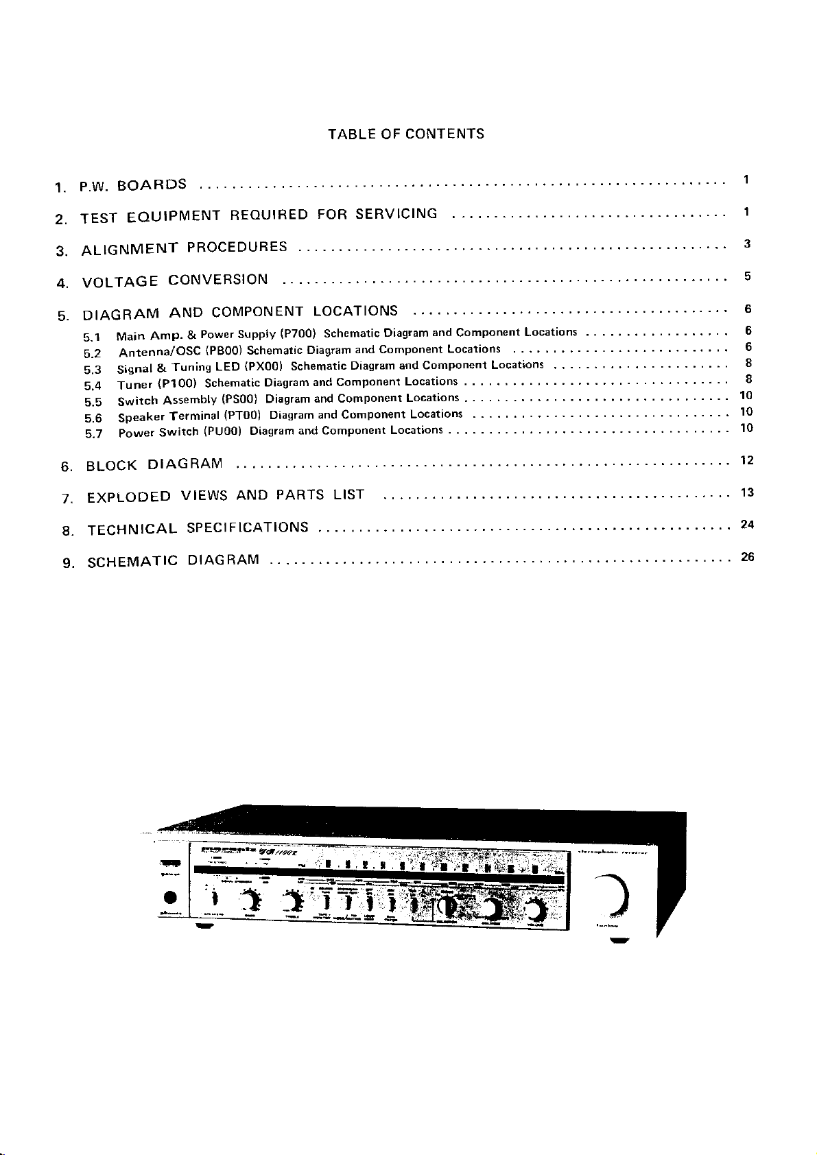
1.
2.
BOARDS
P.W.
TEST
EOUIPMENT
REOUIRED
FOR
TAB LE O
SERVICING
F CONT ENTS
...
'
ALIGNMENT
J.
VOLTAGE
4.
q
DIAGRAM
Main
5.1
Antenna/Osc
5.2
Signal
5.3
Tuner
5.4
switch
5.5
Speaker
5.6
Power
5,7
BLOCK
6.
EXPLODED
TECHNICAL
8.
9.
SCHEMATIC
PROCEDURES
CONVERSION
AND COMPONENT
Power suppty
&
Amp.
{PBOO)
Tuning
&
{P100)
Assembly
Switch
DIAG
Schematic
Terminal
(PUOo)
RAM
VIEWS
SPECIFICATIONS
DIAG
Schematic
(PX00)
LED
(PS00)
(PTO0)
. .
AND
RAM
Diagram
Diagram
Diagram
Diagram
.
LOCATIONS
(P700)
Schematic
Diagram
Schematic
and Component
and component
and Component
and Component
Diagram
and Component
PARTS LIST
Diagram
Locations
and
Component
Locations
and Component
Locations
Locations .
Locations
.
Locations
.
Locations
'
- - " ' 6
"'---
" " "
"
" " '
" " "
. .
"' 6
8
I
10
10
l0
13
26
1
"-
a
Page 4
INTRODUCTION
't.
P.w. BoABDS
service
This
Warranty Stations
lMarantz
Servicing
manual
perienced
carefully.
good understanding
a
parts
The
parts
may
description
tained
TEST
2.
table
This
Alvl Signal
manual
SF1
lvlodel
information
intended
are
technician
atternpt
No
{urnishes
list
ordered
be
included
is
through
local
EOUIPMENT
the
lists
Item
Generator
Test Loop
FIM Signal
Oscilloscope
FrequencY
Circuit
DC
AC
Generator
Cou
Tester
VTVM
Wattmeter
AC Ammeter
Voltmeter
Line
Variable
Shorting
Output
Autotransformer
Plug
Load
r0.5%, 100w)
Output
10.5%,
Load
100w)
prepared
was
and contains service
100L
Stereophonic
and
for use by the knowledgeable and ex
All instructions should be
only-
should be made to
of the operation of
information by which replacement
Jrom the N4aranlz Company. A simple
parts
for
suPPliers
test equipment
nter
for
use by Authorized
information for
Receiver.
voltage
which
REOUIRED
required for servicing
Sound
Tektronix Model T932
Philips l,.4odel 3232
Fluke Model 19004
Flukp l\,4odel
f\4odel 313, Triplet Model 801
included in this
data
proceed
the receiver.
can usually be ob'
FOR SERVICING
Manufacturer and Model
Technology
8000
Simpson Model
Commercial Grade
Simpson
Model 1359
Superior Electronic Co.,
Powerstat
Use
across center
Commercial Grade
Commercial Grade
l\4odel 1 168-10A
phono plug
pin
read
without
the N4odel SR
No.
"Dig.tal"
Simpson
1379
(1-10A)
with 600-ohm
and shell
As can be seen from the
l4odel SR1100L
mounted
square enclosed by a bold dotted line on the circuit diagram.
1. Tuner . . - mounted on P-W. Board P100
2.
3. Volume/Balance Push
4.
5. Tuning LED . . . .. .. mounted on P.W. Board PX00
6. Antenna Coil mounted on P.W. Board PB00
7. Power
on
Main
Amp/Power Supply
Speaker
100L Receiver'
1
cons]sts of the
printed
a
Terminal
Switch
Signal
Use wlth
Signal source
Stereo
shootrng
Distortion measurements
Sinewave
Voltage measurements
Waveform
ASO
MPX Oscillator adjLrstment
Trouble shooting
circuit
. mounted on
Switch
. . . . mounted on P.W. Baord
source for AM alignment
AM
Signal Generator
for FM
separation alignment and troLrble
and squarewave signaJ sourc-"
analysis and trouble
alignment
Voltage measurements
lvlonitors
lMonitors amplifier
cond ition
Monitors
am
Adjusts'evel ot
Shorts
p
rcKLr
Provides 8-ohm
termrnar ron
Provides 4 ohm oad for amplifier output
rermtna( ton
primary power
potential
p
lifier
pr
amplifier input to eliminate
p
load Jor
diagram the chassis of
circuit
following
board
mounted on P.W. Board PS00
mounted on P.W. Board PU00
Use
alignment
lAC)
units. Each
is described within the
P.W. Board P700
PT00
shooting and
(VCO
)
(DC)
to amplif
output
of
mary
under short crrcu t
primary power
power
amplifier
ier
to
to dmp
norse
output
if er
unit
Page 5
SRl1OOL
TUNER
BOARD
P.W.
g
@
Mwlw
@@
[.]
I l@*
Mw
Lw
I I
wl--lw
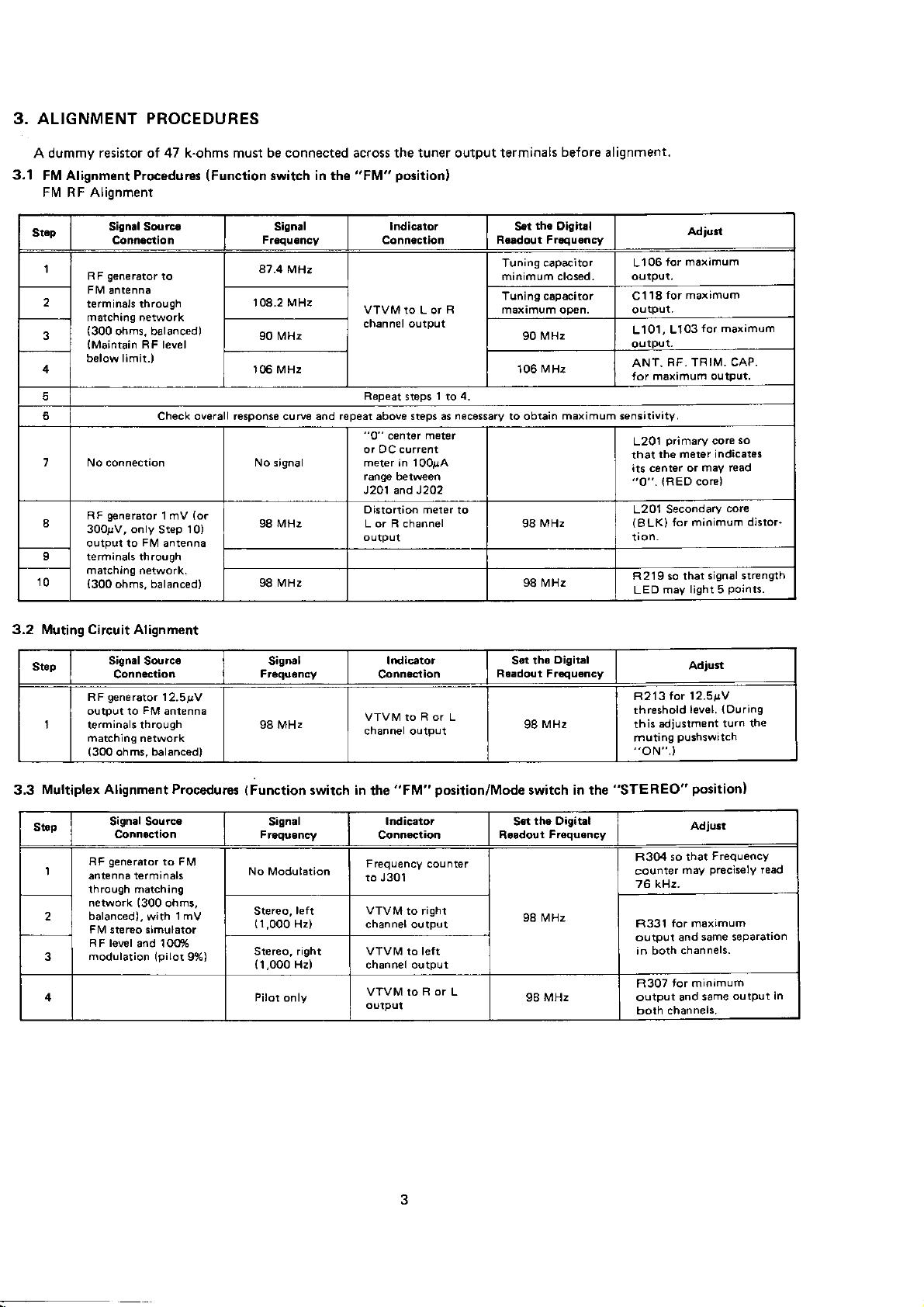
Figure 2.
Adjustment
Point
Locations
Page 6
3. ALIGNMENT
PROCEDURES
A dummy
3.1
FM Alignment Procedures
resistor
47 k-ohms
of
must
(Function
be connected across the tuner output terminals
"FM"
switch in the
position)
Flvl RF Alignment
St€p
I
2 108.2 MHz
4 106 MHz 106
Signal So0rc6
Conneclion
generalor
RF
terminals through
matching network
(300
lMaintain
below limit.)
to
ohms, balanced)
RF lev6l
Signal
87.4
MHz
90 lvlHz 90 lvlHz
5
6 Check overall response curve and repeat above steps as
1 No signal
g€nerator
8
10
RF
300pV, only
outpul lo
terminals th.ough
matching
ohms, balanced)
{300
1mV
Step
Flvl
antenna
network,
{or
10)
98 MHz
98 lvtHz 98 MHz
Indicttor
Connoction
channel output
Repeat
steps 1 to
"0"
or DC current
merer in 100pA
J2O1
Distortion meter
L or R channel
ourpur
center
J2O2
and
meter
4.
necessarv
to
before alignment.
rhe
oigitll
s€(
Roadout
Frrquonry
Tuning capacitor
minimum closed.
Tuning cepacitor C
M
Hz
98 MHz
maximum
sensirivaty,
to obtain
Adrurt
for maximum
L106
outpui.
maximum
118lor
outpur,
for maximum
L103
L101,
RF. TRIM. CAP.
ANT.
maximum output,
tor
primery
L2O1
the meter indacales
thal
its center or
"O".
(RED
L201 Secondary
(BLK)
R219 so that
may light 5
LED
core
may read
core)
for minimum
sign6l strength
so
core
distor-
points.
3.2 Muting Circuit Alignment
Stop
Multiplex Alignment Procedures
3,3
Stop
2
Signal Source
Connection
generator
RF
output to
terminals through
matching network
(30O
Sign.l Source
Connoction
generator
RF
antenna termrnals
through matching
network
balanced),
Fl!4
stereo simulator
RF level
modulation
FM
ohrns,
(300
and 1 0096
12.5pV
antenna
balancedl
to Flvl
ohms,
with
{pilor
1mV
9%)
Sign.l
98 MHz
(Function
Signal
left
Stereo,
(1,00O
Hz)
Stereo, right
Hz) channel output
{1,0O0
Pilot
only
switch in
lrdicator
Connection
channel output
"FM"
the
Indicator
Connoclion
Frequency
to J301
VTVM
output
counter
to right
Set ths
R€adoul FrGqu€ncy
98
position/Mode
$t
R@doui
98 MHz
98 MHz
Digiral
MHz
switch in the
rha oigit.l
Frequency
tor 12.5pV
F.213
threshold
adjustment
this
pushswitch
muting
"oN".)
"STEREO"
so that
R304
counter
76 kHz.
lor maximum
R331
outpul and
in both channels.
tor minimum
R307
output and
both channels,
Adiun
(During
level.
turn the
position)
Adjust
Frequency
preciselY
may
same separatlon
output in
same
re6d
Page 7
3.4 AM
'1
. AM
Alignment Procedures
(Function
lF Alignment
iwitch in the
"AM"
position)
Stop
1
Sign.l So(l
Conn6ction
Sweep
OSC Variable
rc.
generator
Cap.
to
2. MW RF Alignment
Signal
St.p
Apply the signalto
the AM bar antenn€
from rhe RF
using
as
4 1,400
Conmction
the test
per
the
Sourca
generator,
loop.
Figure
2.
Sign.l lndicator
450
kHz marker Oscilloscope
Signal lndic.tor
kHz
520
1,630 kHz
600 kHz
Connsction
Connoction
channel
to T.P. Ouiet
Reado0t
Tuning capacitor
minimum
Tuning capacitor
output
kHz
Rep€at steps 1to 4 d necessary to obtain maximum
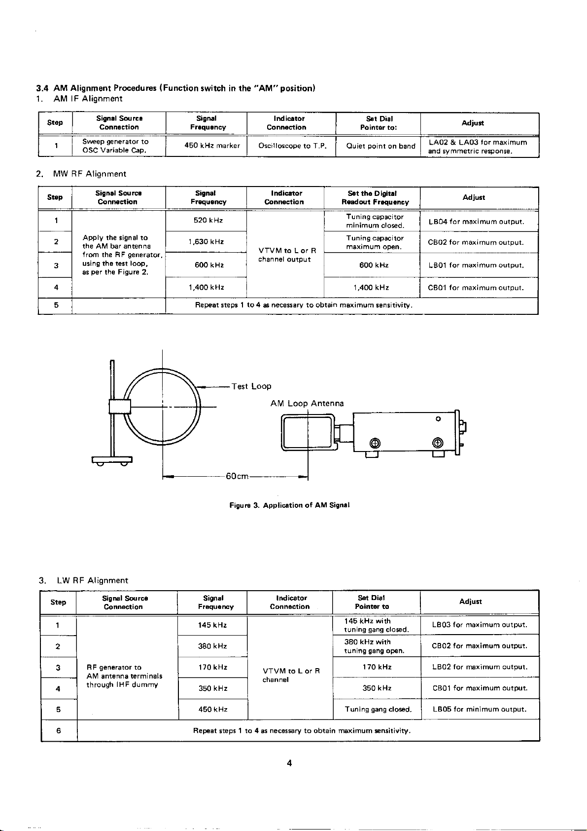
Test Loop
Al\4
Loop Antenna
Sor Dbl
Pointer toi
point
on
S€t tho Dioir.l
Fr€qu6ncy
closed.
kHz
600
kHz
1,400
sensitivity.
band
LA02 & LAO3
ano symmetflc response.
for maximum output,
LB04
CBO2 for maximum output.
for maximum output.
LB01
for
CB01
Adiun
for m6ximum
Adjust
maximum output.
LW RF Alignment
3.
Stop
I
Sigrul SoU
C,onn€ction
rce
2
g€norator
RF
Alvl an'tenna
4
through
IHF
to
t6rminals
dumrrry
5 450 kHz
Signal
FigurB
3. Application
Connection
of AM Signtl
lndic€tor
145 kHz
kHz
380
't70
kHz
kHz 350
350
Rep€at
steps
1 to 4
necossary to obtain maximum senritivity.
as
ohl
Set
Pointor to
'l45
kHz
tuning
kHz with
380
tuning
wirh
gang
gang
closed.
op€n.
Adjun
L803 for maximum output.
for maximum output.
CB02
170 kHz LB02 for rmximum outpul.
Tuning
kHz
geng
clos6d. LB05 for minimum output.
CBo1
for
maximum
output.
Page 8
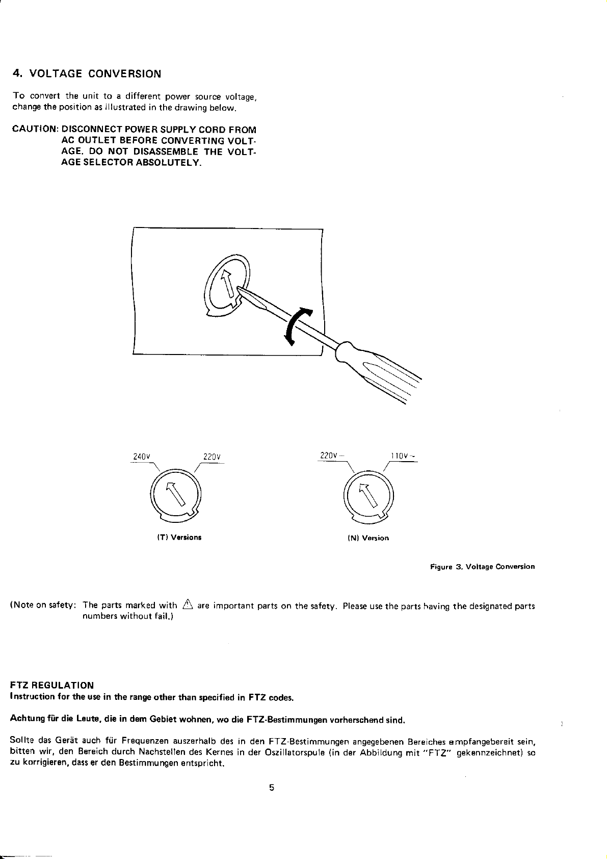
4. VOLTAGE
To
convert the unit
change
position
the
CONVERSION
to a djfferent
illustrated
as
power
in
the drawing
source
below.
voltage,
CAUTION: DISCONNECT POWER
AC OUTLET
AGE. DO
AGE SELECTOR
BEFORE
NOT DISASSEMBLE
ABSOLUTELY.
SUPPLY CORD
CONVERTING
THE
FROM
VOLT.
VOLT-
(Note
on safety: The
numbers
FTZ REGULATION
Instruction
Achtung
for
the use in the range
fiir die Leute,
Sollte das Gerat auch
bitten
wir, den Bereich
zu korrigieren,
dass er den Bestimmungen
220v
(T)
V€rsions
parts
marked with A are important
without
die in dem
fiir Frequenzen
durch Nachstellen
fail.
)
other
than specified in FTZ
Gebiet wohnen,
auszerhalb
des Kernes
entspricht.
?2AV
parts
on the safety. Please use
codes,
wo die FTZ-Bestimmungen
des in den
in der
FTZ-Bestimmungen angegebenen
Oszillatorspule
-
vorherschend
(in
der Abbildung
the
parts
Figure
having the
Voltage Convstsion
3,
designated
sind.
Bereiches empfangebereit
mit
"FTZ"
gekennzeichnet)
parts
sein,
so
Page 9
DIAGRAM
5.
AND COMPONENT
LOCATIONS
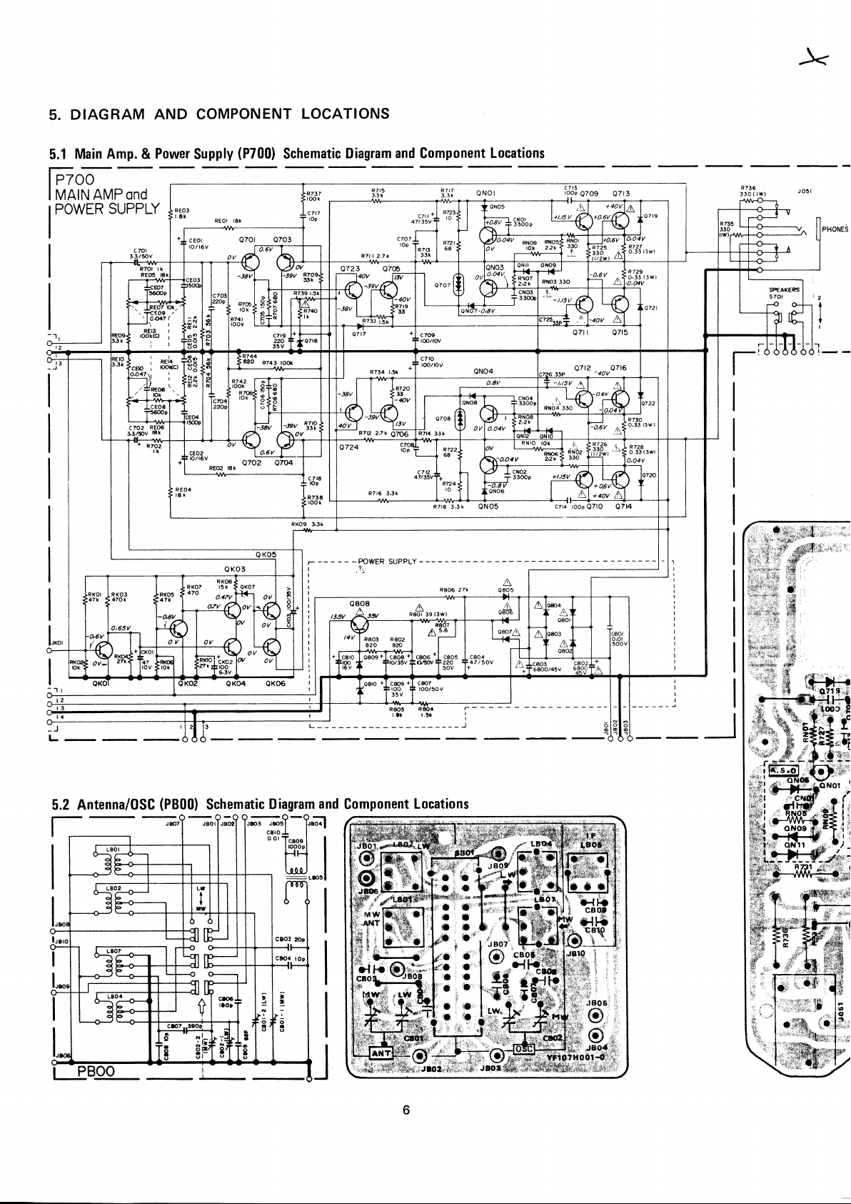
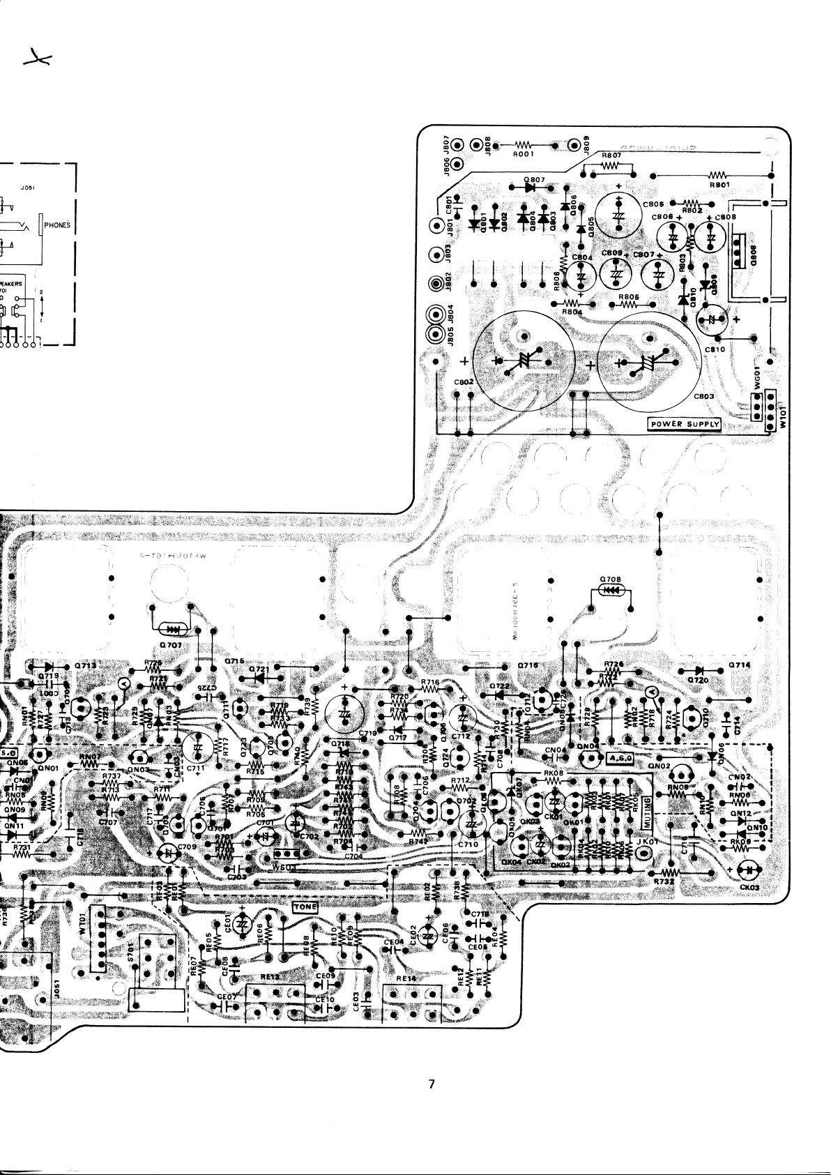
Main Amp. &
5.1
Woo
I MAIN
AMP
POWER
Power
ond
SUPPLY
c 71rl
3,3/fiv
Supply
(P700)
QKO3
Schematic Diagram
Q723 Q705
and Component Locations
POWER
SUPPLY
R 7t7
3,3
RzrB
r
3,3x
oNol
QNO5
c713
roop
e7O9
,\
+t,p v
fr
o7r r 0715
czrq roop
QTIO O7l4
07t3
R736
330
(
lw)
5.2 Antenna/Os0
(P800)
Schematic
Diagram
and
Component
A
(3W)
R80t
39
Locations
j
Page 10
j<
1
tT
-'ll
l--a I
'l
I
-l
Page 11
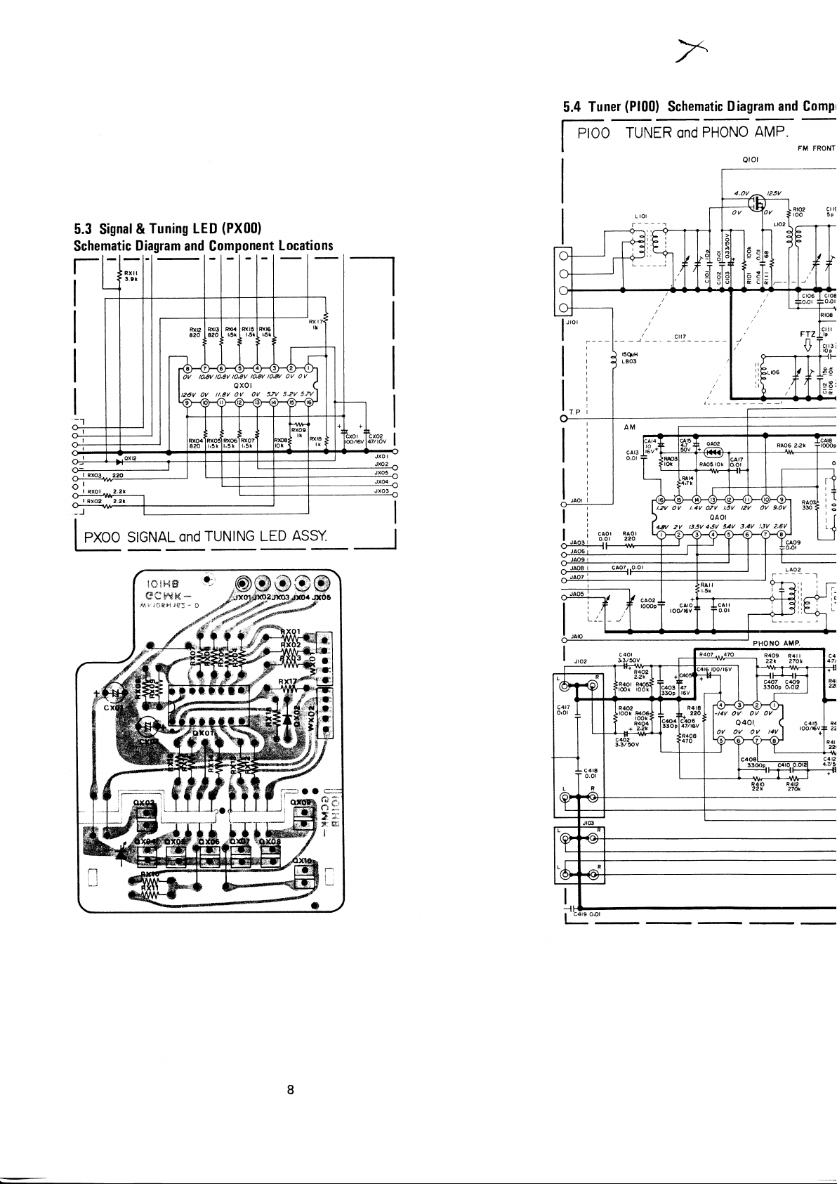
Tuner
5.4
l-----
PIOO
I
I
(P100)
TUNER ONd
Schematic
PHONO
Diagram and Compr
AMP.
FM
FRONT
5.3 Signal
Schematic
&
Diagram and
SIGNAL
Tuning LED
Component
to,8v
toav
ov
t26V
il,8v
Ot/
TUNING
ond
(PX00)
to,w to'av ov ov
to,8v
OXOI
OV OV
LED
Locations
I
5,2V 5,7V
5?V
ASSY
Lzv ov
48V 2V
t,4v
t3.5V
+
t,sv tzv OV
o7v
4,5V 54V
3.4V
g,OV
/3V 2'6V
OV
OV OV
I4V
Page 12

l0) Schematic D iagram
and
Component
Locations
NER ond
Lzv
t,4v
oy
/J,5V 46V 54V 3,4V
4AV 2V
PHONO
oc,
a
t,sv
tzv
o7y
AMP.
9l-
l-
clc
g,ov
ov
tJV
2,6V
FM
FRONT
END
.LIfi
Fzor
6
|
(\I
|
c
ov 3av 2,6v 2,6v
IJV
30v 5.4v
J
tci
:
n
o
ol
c
2.4V z6V 23V
&4v &4v
//,2v
ov 23v
OAV
FM
IF
o,4v 5v ov 5,6v
v 2,7V 2,7V 0V
Rstr
^^^zn
MUTIXG A.O.J
5v
Q204
t.gy
t4v
55V
x
o
g
o
s
A'
C!
o
E
5,6v 56v
5.6V 5.6V
O3O5
19
R2
3k
SIGNAL LED
A
F.220
k
2tl
-ti
\,
JzOI
OJ
ffi_53"112
ov ov ov
PI{ONO
t4v
AMP.
R328
3,3k
0306
FM_l
POSITION
fPHoNol
SELECTOR
+
3
,!
ro
t2
lrl
1
ws02
r!
TAM_l f
I-AUXI
,.rrtrau
-L
!r
3
r
wtot
Page 13

x
lf llo
l
,f.'
,:
! ;: i.
,1f,,1
|
f
il
,++l#
*
lo*'q.ot
;:r.$is?s.s?,i1;#r.iii"r!F+":ii,-q:.sq,.:.!;l#ff&'11#+,
,r-Q|{l/
fffil
Hi
#
i
,6rrii
=;-I*p
ffi#
5.5
iOr
l-
lL_
lrAP€
Assembly
Switch
I
TAP€
I
I
souRcE
rcLrroR
PSOO
n****r*o@*
(PS00)
ST N,,T./UOT€
Schematic
IUT.
LOUDNESS
10
Diagram
and Component
Hi-FILTER
I
I
MW/
I
I
I
I
..--r..,! -
Locations
LW
-l
Page 14

>{
5.6
Speaker
Schematic Diagram
Terminal
and Component
(PT00)
Locations
Switch
(PU00)
and Component
Power
5.7
Schematic
Diagram
l-Fh--l
tSEryed
Locations
11
Page 15

BLOCK
6.
DIAGRAM
H
I
c)
Lrj
o
u
J
5
(c
0
=
J
z
0
z
l
(9
F
6
0
a
t!
26
lrJ
-
-(L
I
)QACI OQQ
;l(
U_
F
Q
Lf_
a
N
=
ITJ
a
@
C
Z
gJ
F
S;
f,E
tu
6
(r
IJ
J
JF
E93
i35
(L
o-
J
lJ.l
lr)
=
u,
E
o
o
Lr,,
J
FI
JJ
fiF
Xu
UJJ
o.r!
aa
5;
t
f
u
\
g
u
UJ
I
\
z
o
l-
IE--]
(9F
z_=
F(J
>c
=6
E€
3r
(J
UJ
zl-
3=
ffK-/
l*=
l@E
-J- lrr
t_J4i;
I
H
=
a
lrj
o
o
=
t
o
F
z*.
(L
=
5
=
(L
=f;
is
otr
=t
il(/)
F
(r
o
26
=p
c
o
F
|J
t!
J
t!
a
-
L)
Efr
(l:C
trF
o
g
=
l.L
o
z
ttJ
F
z
=8
lI- ll
Lgls l;J
(L
=
ll-
(r
=
c
=
o
z
o
I
(L
oi
7,xoz
Yf,IrJllI
E
1-
FF
12
Page 16

7. EXPLODED
VIEWS
AND
PARTS
LIST
7.1
[C01-99]
Front Panel
o02B
ffi_
ooau-\
REF,
DESIG.
A
o01 B
o02B
B
oo4B
oo5B
O'TY
N
I
1
2
1
1
1
PART
T
1
105H063400
1
1 05H06301 0
2
403H06701 0
t
1 07H063400
1
1
07H06301 0
1
105H1580tO
oilB
NO. DESCRIPTION
Front
Panel, Assembly
Escutcheon, Front Panel
Cap, Panel Side
Dial Panel Assembly
Escutcheon, Dial Panel
Window
orsa
REF.
DESIG.
0B
01
01 1B
48
01
01 8B
9B
01
003G
I
O'TY
N T
4
1
I
2
2
'l
mh
o
o
PART NO. DESCRIPTION
4
1
1
2
2
3
1 54020
1 05H
403H 1 54020
1 05H 1 54060
51 30030680
51
30030680
28030880
51
Knob, Bass, Treble,
Knob, Tuning
Knob,
Selector
P.H. Tapped
P.H. Tapped
B.H.Tapped
(
N
(T):
):
Screw
Screw
Screw
for Europe
for
United
Vol., Bal.
P3 x 6
P3
83 x 8
Kingdom
x
6
13
Page 17

7.2
[C02-99]
ToP
Gover
REF.
DESIG.
O'TY
N T
?
ot4D
PART
oo3D
oozD I -.-'
-\@@Y{,-
Y N
ooSD
ooz*ASg-oo6D
NO.
DESCRlPTION
ooSD
r4D
REF.
DESIG.
*-->'a{-oozo
."'
O'TY
N T
NO. DESCRIPTION
PART
.2
r
o
,a
(N):
for Europe
(T):
for
00rR
United
o07D
Kingdom
D
001
002D
003D
004D
005D
o06D
007D
008D
014D
R
I
4
z
'|
4
a
2
K
208H257010
1
4
51
2
2991259110
1 05H25701
1
403H
4
51
29651
2
208H05601
2
R
51
260408U0
0
05701 0
28030880
18010
0
28030880
Top Cover
Lid,
B.T. Screw
Bushing
Lid, Buttom Cover
Leg
Tapped Screw
B.H.
Spacer
B uffer
Tapped Screw 83 x 8
B.H.
84x8
83 x
001
002R
2932861
1
1
25788610t0
1 1 0
Top
Label,
Label, Bottom Cover
Cover
14
Page 18

7.3
[C03-99]
JO9l
Panel
Bear
005E
s't{
REF,
DESIG.
E
001
E
001
oo2E
003E
004E
005E
007E
008E
009E
0E
01
012E
4E
01
O'TY
N
o
4
4
2
2
2
2
1
1
1
sry
NO.
PART
T
1 07H 1 6021
'107H160220
1
51 280308UO
b
51
4
51
4
51
z
51
2
51
51
2
2112265010
1
29'12259020
1
4581 86
1
280308UO
280308U0
280308UO
280308UO
420308TO
280308UO
0
1 01 0
PTOO
DESCRIPTION
Bracket.
Bracket,
B.H.
B.H.
B.H. Tapped Screw
B.H. Tapped Screw
B.H.
O.C.H.
B.H. Tapped Screw
lndicator
Bushing
Rear Panel
Rear Panel
Tapped Screw
Tapped Screw
Tapped Screw
Tapped Screw
Made in Japan
Label,
83 x 8
x 8
83
83 x
83 x
83 x 8
03 x I
83 x 8
E
oo3E
ige'r/':/
oo3R
'--
o/ogE
ot2E
-
A1 owe
rE
oo
LOs1
O'TY
N
1
1
1
I
1
PART
T
1
4204A61020
I
FS
YJ08000290
1
Y L0301
1
YP04000590
1
8Y05060040
I
8Y05030030
LA0001 501 0
1
NO.
1 0080800
0250
Label
Fuse T800mA
Fuse
Jack,
Terminal,
AC Inlet
Plug,
Voltage Selector
Voltage Selector
Ant.
Loop
REF.
DESIG.
003R
AFOOl
8
8
AJOOl
JO31
AJ043
AJ091
AJOg1
\
oo2E
(N):
o
for Europe
(T):
o
for
United
DESCRIPTION
Holder
GND.
Kingdom
t5
Page 19

7.4
[P01-99]
,\\
orle
General Parts
Front
Ghassis
and
o05G
r}Nf'&44\
)\_
K"W
\\-r\
\
^.{-oo4i
t6
ob4F
>)\S/.-'
tJ./.
v,/ ,,
{i./ .'
"ii'."
IG
,mS- \
Y,
*../q
6g
or4G
REF,
DESIG.
0078
0088
004F
G
001
002G
o05G
006G
008G
009G
010G
1G
01
2G
01
3G
01
O'TY
N T
I
6
2
1
I
2
2
t
2
1
1
1
I
I
PART
208H
I
05H
o
1
28030680
51
05H
1
1
1 05H
1
5't
2
51
2
105H1
1
260308B0
sl
2
1 05H
1
51
1
,
22760,05050
105H118020
1
NO.
1 54060
0
1 5401
1
0
6001
0
1 2001
100306A9
100306A9
18010
1 60020
28030880
DESCRIPTION
Knob, Power Switch
Knob, Push Switch
B.H. Tapped Screw 83 x 6
Bracket,
I
B.H.M.
B.H.M. Screw
Spacer,
B.T. Screw
Bracket
B.H.
Clamper
Spacer
Front Chassis
nsu
lator
Screw
LED
Tapped Screw 83 x 8
83x6
83x6
83x8
REF.
DESIG.
014G
5G
01
017G
018G
019G
o21 G
i
001
002i
i
003
004i
sv02
O'TY
N T
1
J
I
z
I
1
I
I
1
1
1
PART
1
2259262500
2276262500
1 05HO5301 0
1
2
2912259020
1
1 05H
I
1 05H2730
403H 1 0301 0
1
403H118010
1
1
403H303020
1
403H303030
1
sR00040080
(N):
o
for Europe
(T):
r
for
NO. DESCRlPTION
Pulley
Pu lley
Pointer
Cover,
Bushing
t 0
nsu
I
lator
Flywheel
Pointer
Spacer
Mask
Mask
Rotary
Switch, Selector
1 20020
United
Kingdom
16
Page 20

?.5
[P02-991
oosL
Chassis
g
and 0ther
Parts
K.'
l---\
.-lororr
\-r
r5F
or5
(N):
r
(T):
I
REF.
DESlG.
oo1
oo2F
003F
004F
007F
008F
009F
01
01
012F
01
014F
01
01
01
01 9F
020F
o21F
o24F
o25F
026F
o27F
038F
039F
o40F
01 6E
01
ool
{or
for
F
0F
1F
3F
5F
7F
8F
7E
F
Europe
United
O'TY
N T
1
1
1
1
1
3
3
4
4
4
4
1
1
1
1
1
1
1
1
2
2
2
2
4
4
1
1
1
1
1
1
I
1
I
1
2
2
'l
1
1
1
I
1
'|
1
2
2
2
2
I
1
1
1
Kingdom
NO.
PART
1 2601 0
1 05H
1 26020
05H
1
't
126030
05H
28030680
51
26030880
51
26030880
51
805601
221
202H267030
2803088O
5't
1 05H00401
28030880
51
2603088O
51
260408UO
51
28030680
51
1 00501 0
287
72040805AO
59010
403H1
12115020
21
09040
22591
28030680
51
62030049W0
28030880
51
1 07H 1 6001
2803088O
51
26030880
51
1 2001 0
208H
1 0901
1 05H
DESCRIPTION
Left
Stay,
Right
Stay,
Center
Stay,
Tapped
B.H.
B.T. Screw
B.T. Screw
0
Buffer
Heatsin k
B.H.
0
Table,
B.H.
B.T. Screw
B.T. Screw
B.H. Tapped Screw
Clamper
String
Drum, Dial
Spring
ield
Sh
B.H. Tapped Screw 83 x 6
Lug
B.H.
racket
0
B
B.H.
B.T. Screw
nsu lator
I
ield
0
Sh
Screw
Tapped Screw
Transformer
Tapped Screw
(
1 35)
Tapped Screw 83 x 8
Tapped
Screw
P700
ooTF
83x6
bJ x d
83x8
83 x 8
83 x 8
83 x 8
84 x 8
83 x 6
83 x 8
83 x
f
8
l-\ &
-l
\-oozr.-'
q
002L
\---
REF.
DESIG.
001
002L
003
LOOl
A
ALOOl
or7\
o,rr/"r_
\
oll
O'T\
N T
I
L
4
4
L
PART
1
1 05H26701 0
4
51 28031080
4
51 28030880
TS1
,|
TSl
NO. DESCRIPTION
k
Heatsi n
B.H. Tapped Screw 83
B.H. Tapped Screw 83 x 10
Power
6626020
6626060
Transformer
Power Transformer
x 10
17
Page 21

7.6
[H01'99]
Packing
Materials
o02T
<-
\-/
oolT
REF.
DESIG.
s
001
003s
006s
0s
01
35
01
95
01
0017
0027
0037
0037
0047
O'TY
N
1
2
I
1
4
I
I
1
t
PART
T
1 07H801
001
2
9090909040
291
1
9526019060
2731821010
1
1
105H851
I
1 05H851
07H85601
1
I
9630000200
a
1 07H85601
NO.
0
01
H809010
07350
81
310
320
0
0
DESCRIPTION
Case
Packing
ion
Cush
Polyethylene
Sheet
Serial
Sil
nstructi
I
nstru cti
I
Circuit
Guarantee
Circuit
No.
icagel
Card
on s
ons
Diagram
Card
Diagram
Sheet
^,,"o13t
DESIG.
AWOOl
AWOOl
REF.
v
o01
O'TY
N T
1
1
oo3s
PART
1
2A02000070
zco1
1
zc01
NO.
805030
804030
at
//'-\</oo4T
\>
(N):
r
(T):
o
DESCRIPTION
EXT. Antenna
Cord
Power
AC
AC
Power
Cord
o03T(N)
003T(T)
Europe
for
for
United
Kingdom
18
Page 22

ELECTBICAL
7.7
REF.
DESIG.
O'TY
N
T
PARTS
NO. DESCRIPTION
PART
REF.
DESIG.
O'TY
N
(N):
o
for Europe
(T):
r
for
United Kingdom
NO.
PART
T
DESCRIPTION
P100
cAo1
cA02
cA07
cA09
cA10
cA1
cA12
cA13
cA14
cA15
cA16
cA1
cA18
cA19
cA20
cA21
c101
c102
03
c1
04
c1
05
c1
cl06
07
c1
08
c1
09
c1
10
c1
11
c1
c112
c1 13
c1'14
c115
c116
c1't7
ct 18
c119
c201
c202
c203
c205
c206
c207
c208
c209
c21o
c21
c212
c213
c214
c21 5
c216
c217.
c301
c302
PlOO.TUNER
I
1
1
I
1
1
1
1
1
1
1
t
I
1
I
1
1
1
I
1
1
1
1
YG 1 05H001 0
zz107Haol0
DA17103010
DK16102300
DA17103010
71 0301 0
DA1
EA1 0701 630
71
DA1
0301 0
D 1 5680370
D
DA17103010
EA 1 0601 630
EA47505030
EA33601
K1 81 03320
D
DK16t02300
D F 1
6333300
F 1 7333300
D
DF17103300
DD11100300
71
DAl
0301 0
I
1
1
1
1
1
1
1
1
1
1
1
7
1
1
1
1
1
EA33405030
71
DA1
I
1
1
1
1
1
1
1
1
1
I
1
1
1
I
1
1
1
I
1
1
1
I
1
I
1
I
1
1
1
'|
1
1
I
I
1
1
1
1
I
1
1
1
1
1
t
1
1
1
1
'l
1
,|
1
1
1
I
I
I
1
1
1
1
1
1
1
0301
DD15150300
DAl 71 0301 0
DD15301360
DDl 5200300
DA 1 71 0301 0
EA10701630
DD10010370
5200340
DD1
DD11100300
DD15300310
DD15150300
t 7103010
DA
cA32200060
cT1 1000080
D 1 0050370
D
DA17103010
7103010
DA1
71 03010
DA1
71
DA1
0301 0
EA22505030
71
DA1
0301 0
DAt7103010
EA 1 0505030
DA 1 71
0301 0
DA17103010
D K 1 8403320
DK 1 8403320
EA22505030
DD 1 5300370
e447405030
DA17103010
EA 1 0601
DA17103010
P.W.
Board. Tuner
P.W. Board Assembly
PlOO€APACITORS
Ceramic 0.O1uF
Ceramic
Ceramic 0.01pF
Ceramic
Elect
Ceramic 0.01pF t2oo/o
Ceramic
Ceramic
Elect
Elect
Elect
630
Ceramic
Ceramic 100OpF
Film
Film
Film
Ceram ic l Op F t0.5p F
Ceramic 0.OlpF x2Oo/o
Elect
0
Ceramic
Ceramic 15pF +5o/o
Ceramic
Ceramic
Ceramic 2OpF
Ceramic
Elect
Ceramic
Ceramic 20pF x5o/o
Ceramic 10pF ro.spF
Ceram ic
Ceramic 1SpF
Ceramic
Variable FM-3,
Trimming 10pF
Ceramic
Ceramic 0.01pF
Ceramic
Ceramic
Ceram ic
Elect
Ceramic
Ceramic 0.01pF
Elect
Ceramic
Ceramic
Ceramic
Ceram ic
Elect
Ceramic
Elect
Ceramic
630
Elect
Ceramic
CI RCUIT BOARD
x2Oo/o
100OoF
0.01uF
100uF 16V
0.01sF
0.01pF
0.033pF
0.033pF
0.01pF
0.33pF 50V
0.01pF +2Oo/o
0.O1pF
3O0pF
0.O1pF
100pF
0.01pF
0.01pF
0.01pF
0.01pF
0.01pF
0.01pF
0.01pF
O.O
Q.O4qF
2.2pF
O.47
0.01pF
0.01r^lF
tloo/o
x2Oo/o
t2oo/o
x15o/o
68pF
t2O%
OpF
l
4.7 p.F
33pF 16V
+80o/o-2OYo
{e/,
+1Oo/"
t2Oo/o
x2Oo/o
t2oo/o
t5o/o
+5%
x2O%
t0.25pF
1pF
30p F +5o/o
t,o/o
+2Oo/o
AM-2
to.2spF
SpF
!2oo/o
!2oo/o
tzOo/o
x2Oo/o
2.2pF
x2Oo/o
t2Oo/o
1pF 50V
*2Oo/o
t2oo/o
pF +8Oo/o-2Oo/o
+8O%-2Oo/o
!5o/o
30pF
pF
!2O%
10pF
t2oo/o
16V
50v
l6V
50V
50V
50V
16V
c303
c304
c305
c306
c307
c308
c309
0
c31
c31
c312
c313
c314
c31 5
c316
7
c31
8
c31
c31 9
c320
v5z I
vSzz
c323
c324
c401
c402
c403
c404
c405
c406
c407
c408
c409
c410
c411
c412
c413
c414
c415
c416
c417
c41A
c419
RAOl
RA03
RA04
RAO5
RA06
RAOT
RAOS
RAO9
RA1 O
RA1
RA12
RA1
R101
R102
R 103
R 104
R105
I
1
I
1
I
I
1
1
1
1
I
1
1
1
I
1
1
1
I
1
1
1
I
1
1
1
1
1
I
1
1
1
1
1
1
1
1
1
1
1
1
1
I
1
I
1
1
1
1
1
1
1
1
1
'|
1
1
1
1
1
I
1
1
1
1
I
1
1
1
1
1
1
1
1
a
I
I
1
I
1
I
1
1
1
1
1
I
1
I
1
I
1
GDOs1 04140
I
1
GD051
I
1
1
GD051 521 40
1
1
1
1
1
1
1
I
1
I
I
1
1
GD051 01 140
GD05332 1 40
GD05104140
GD05101 140
GD05223140
GDO5472140
GD051 021 40
3
1090
DF5551
DFs5821 090
EA47503530
EA 1 0505030
EO10505010
EA
1 0505030
EA22701
630
EA 1 0505030
DF16153300
DF16153300
EA47405030
E447405030
EAl 0601
630
EA10601630
DF 1
6332300
DF 1 6332300
DA161 81 01 0
DA16181010
EA22505030
EA22505030
DF 1
02300
61
DK16102300
EA33505030
EA33505030
DA1 633 1 01 0
DA16331010
EA47501
630
EA47601 630
DF
1 6332300
D F
1 6332300
DF16123300
DF16123300
E447505030
EA47505030
DD
1 51 01 370
51 01
DD1
370
EA1 0701630
EA 1 0701
630
DA17103010
DAl 710301 0
DAI 710301 0
GDO5221140
GD051 031 40
GD05103140
GDO5221140
GD05222140
GD05331
140
GDO5223140
04140
Film
Film
Elect 4.7y.F
Elect
Elect 1pF 50V
Efect
Elect 22OpF
Elect 1pF
Fif m
Fif
m
Ef
ect
Elect
Elect
Elect
Film
Fif m
Ceramic
Ceramic 18OpF t'llYo
Elect
Elect
Ceramic
Ceramic loOOpF
Elect
Elect
Ceramic
Ceramic
Elect
Elect
Fif
m
Fif
m
Fif
m O.O12qF
Fif
m
Elect
Ef
ect 4.7
Ceramic
Ceramic
Elect
Elect
Ceramic 0.01pF
Ceramic
Ceramic
P100-RESTSTORS
(Af
510pF
82OpF
0.01
0.0'l
O.47
O.47
330OpF
330OpF
100OpF
33OpF
330pF
330OpF
330OpF
O.O12pF
0.01pF
0.OlpF
f Resistors
220n
10KO
10Ko
220a
2.2Kn
330f'
22Kdt
'tooKo
100KC}
1.5KC}
100f,l
3.3Ks|
100Ka
100a
22Kn
4.7KA
1Ko
t5o/o
!5"/"
1pF 50V
1pF 50V
SpF
SpF
p.F
pF
lOpF
1 OpF 16V
18OpF
2.2p.F 50V
2.2pF 50V
3.3pF
3.3pF 50V
47pF 16V
47pF
4.7pF 50V
pF
1OOpF
100pF
10OpF 16V
lOOpF 16V
x5lo
are
35V
(NP)
16V
50V
!1io/o
tloo/"
50V
50V
16V
tlOo/o
*.1Oo/o
x'lO%
tlOo/o
!1oo/o
50V
t18/o
tlOo/o
16V
tloo/o
xlOo/o
!1Oo/o
tloo/o
50V
xiY"
x5Vo
+2O%
t2O%
t2O%
and 7"W)
19
Page 23

REF.
DESIG.
O'TY
NIT
PART
NO,
(N):
r
for Europe
(T):
o
for
United
DESCRIPTION
Kingdom
R106
R107
R108
R109
R110
1
R11
R 112
R113
R201
R202
R203
R204
R205
R206
R207
R208
R209
R21
R21
nzlz
nztJ
R2't4
R21
R21
R217
R21
R219
R220
R221
R301
R302
R303
R304
R305
R306
R307
R308
R309
R31
R31
R3l2
R31 3
R31
F31
R31
R318
R319
R320
2.2Ka
100Ko
100Ko
470a
470f|
22KA
22KA
270KO
270KO
220Kn
220K{r
220A
220A
220A
220dr
PlOO€EMlCONDUCTORS
tc
Varistor
Diode
F.E.T.
Transistor
Transistor
Transistor
Diode
Diode
tc
Diode
Diode
f c
Diode
0
Diode
Diode
ransistor
T
Transistor
tc
PlOGMISCELLANEOUS
Ceramic
Ceramic
Ceramic
Ceramic
Terminal,
Terminal,
Terminal,
LF.T. Coil
l.F.T.
Antenna Coil,
Coil, FM
FM
Coil,
Choke
0
l.F.T. Coil
OSC Coil,
0
Choke
LF.T. Coil,
Switch
Slide
Rotary Switch
Jumper
LA1240
MV2O3
152473
3SK45B
2SC1047(C)
25C829(C)
2SC829(Cl
152473
152473
LA1231
152473
152473
K84437
152473
152473
152473
2SC945(O
2SC945{O
JRC4558
Filter, 450kHz
Filter,
SFE
Filter, SFE
Filter,
SFE
Antenna
RCA
RCA Pin Jack
Coil
FM
RF
RF
O.75pH
Coil,
FM
3.3pH
Coil,
FM Det
(4P)
Lead,
or
or R}
10.7MHz
10.7MHz
10.7MHz
Pin Jack
R)
(4P)
(4Pl
1
1
1
1
I
1
I
1
1
1
1
1
1
1
I
1
I
I
1
1
1
1
1
1
1
1
1
1
t
1
'l
1
I
1
'l
1
1
1
1
1
1
1
GDO5222140
04140
GD051
GDOs1
GD05471
GDO5471
GD05223
GD05223
GD052741
041
140
140
1 40
1 40
40
40
GD05274'!40
GDO5224140
GDO5224140
GD05221
140
GDO5221140
GG05221
140
GGO5221140
HC1 0041
HV000061
HD20001
HF400451
030
20
210
B0
HT310471C0
HT308291C0
HT308291
HD20001
HD20001
C0
21 0
21 0
HC10028030
HD20001
HD20001
HC 1 0001
HD20001
210
21 0
420
210
HD20001 21
HD20001
210
HT309452A0
HT30945240
HC10008090
F F
1 0045200
FFl 1070530
FF1 t070570
FF11070570
YTo1040230
YT02040260
YT02040260
0730
1 001
Lr
Lt10015060
LA12026170
LL24800030
LK 1 1 800030
LC175100'|0
001 601
Lt 1
LO 1 203601
LC1 3320050
4030020
Ll 1
ss04040040
sR00040080
YUO412026C
40
40
40
1oKs,
5.6KO
47 S7
10KO
100sl
10A
47A
27Ka
330rt
2.7Kn
1 sKA
560s-,
330s}
220d2
1 50Ksl
2.2KA
10Krl
330sl
22KS'L
100Ka
50Ko(BlTrimming
120Kf,
56Kn
18Ks}
820C}
12Ks}
2.7Kc"
22Kdt,
10Kn
47KO
220Ks].
15KO
820s}
4.7K[l"
4.7Ks}
150Ksl
47K',
3.9Ko
10KA
220A
220{t
100Ko
1 00Ksl
10KO
10KO
18KO
18Ko
1oKo
1oKsl
3.3Ko
3.3Ko
390a
20no
100Ko
'l00Ko
100Ko
100Ko
2.2Kd2
Trimming
5Ka(Bl
5Kf,2(B)
5Ka(Bl
Trimming
Trimming
1KO
39s,
R404
11 l1
R40s
l1 ll
R406
ll l1
R4o7
11 ll
R4o8
11 I1
R4oe
l1 l1
R410
l1 l1
R411
l1 l1
R412
11 |
R413
l1 l1
tt
R414
11 |
R415
l1 l1
R416
l1 l1
R417
11 I
R418 l1 l1
oA01
oA02
oAo3
0101
o102
0103
o201
0'202
o203
o204
0205
o206
0301
0302
0303
0304
0305
0306
o401
FAOl
F201
F202
F203
J 101
J102
J103
LAO2
LA03
L1 01
L102
Ll 03
L1 04
L1 05
L 106
L 107
L201
sv01
sv02
w101
40
031
GDOs1
GDO5562140
GDO5470140
GDOs1
GDO4101
03
40
1
'|40
GD05100140
GD05470140
GDO5273140
GD05331
140
GD05272140
53140
GDOs1
GDO5561
GD05331
GD05221
GDOs1
GD05222140
GD051
0
1
GD05331
GDO5223140
GD051
140
140
140
54140
40
031
140
40
041
RAO5030090
24140
GD051
5
6
I
GDO5563140
83140
GDOs1
GD05821
GD051
RA050201
140
23140
60
GD05272140
GD05223140
03140
GDO51
GDO5473140
GDO5224140
RAO5020160
53140
GD051
GDO5821
RA050201
GD051
140
60
02140
RF05390140
0
1
GDO5472140
GDO5472140
GDOs1
541
40
GD05473140
4
5
7
GD05392140
40
031
GD051
GDO5221140
GDO5221140
04140
GD051
04140
GD051
03140
GD051
031
GD041
DOs1
G
GDOs1
1 40
83
83140
GD05103140
03140
GD051
GD053321
GD053321
GD05391
GD05391
GD051
GD051
140
140
04140
04140
GD05104140
04140
GDOs1
GDO5222140
Page 24

REF.
DESIG.
O'TY
N T
NO. DESCRIPTION
PART
REF.
DESlG.
O'TY
N
(N):
r
for
(T):
o
NO.
PART
T
DESCRIPTION
Europe
for
United Kingdom
P700
cE01
cEo2
cE03
cE04
cEoS
cE06
cE07
cE08
cE09
cE'10
cK01
cK02
cK03
cNol
cN02
cN03
cN04
c701
c702
c703
c704
c705
c706
c707
c708
c709
c710
11
c7
12
c7
13
c7
c714
17
c7
c718
c719
c725
c726
c801
c802
c803
c804
c805
c806
c807
c808
c809
c81
PTOO-MAIN AMP. & POWER
YKl05H1610
I
1
22105H1610
1
1
0601 630
EAI
1
1
1
1
I
1
1
1
1
1
1
I
1
1
1
'l
1
1
1
I
1
1
1
I
I
2
2
1
1
1
1
,|
1
'l
I
1
1
1
1
I
I
1
I
1
1
1
I
1
I
1
1
l1
,|
I1
1
lr
1
1
ll
1
lr
1
l1
,|
l1
1
1
I
1
1
1
I
1
1
1
I
I
a
1
,|
1
I
1
I
1
0
0601 630
EA1
DF16152300
52300
DF 1 61
DF16153300
DF16153300
DF 16562300
D F t 6562300
F 1
D
6473300
F 1 6473300
D
EA47601030
EA10700630
E A 1 0703530
7332300
D F 1
7332300
F 1
D
7332300
DF 1
1 7332300
DF
EA33505030
EA33505030
DD1522'1370
DD15221370
51 51 370
DD1
DD't 51 51370
DD11100370
DD11100370
EA1 0701 030
EA1 0701
EA47603530
EA47603530
51 01 560
DD 1
01 560
1 51
DD
1 100370
DD1
1 100370
DDl
E422703530
D 1 5330370
D
5330370
DD 1
DKt8103560
EB68804540
E868804540
EA47505030
E422705030
EA 1 0605030
EA 1 0705030
EA33603530
EA1 0703s30
EAI 0701630
SUPPLY
P.W.
Power Supply
P.W. Board
PTOO.CAPACITORS
E lect
Elect
Film l5OOoF
Film
Film
Fif
Film
Film
Film
Film
Elect
Elect
EIECI
Film
Film
Film 0.033pF
Fif
Elect
Elect
Ceramic 22OpF
Ceramic 22OpF
Ceramic 150pF
Ceramic
Ceramic
Ceramic
Elect
030
Elect
Ef
Ef
Ceram ic 100p F
Ceramic IOOpF
Ceram
Ceramic 1OpF t0.5pF
Elect
Ceramic 33pF
Ceramic 33pF
Ceramic
Elect
Elect
Elect
Elect
Elect
Elect IOOpF
Elect
Elect
Elect 100pF
CIRCUIT BOARD
Board, Main Amp.
Assemblv
lOpF 16V
lQpF 16V
1500pF
0.01SpF
m O.O1SpF
56O0pF
5600pF
pF
O.Q47
yF
O.O47
pF
47
100prF
1 00pF
0.033pF
O.033pF
m 0.O33pF
3.3p.F 50V
3.3pF
150pF
lOpF
1OpF
100pF 10V
1O0pF 10V
ect 471.rF
ect 471rF
ic
10p
22OpF
0.01pF
6800pF
68O0pF
pF
4.7
22Op.F
10prF
33pF
100pF
F 10.5p F
&
t1o"/o
tlOo/o
!1O%
+1Oo/o
x1O%
!1O%
tlQo/o
+1Oo/o
t2O%
r2O%
t2Oo/o
t2Oo/o
t5o/o
t5o/o
t5%
+5o/o
10.spF
r0.spF
t5o/o
t5%
x5%
+5o/o
10v
6.3V
?tr\/
50V
35V
35V
35V
45V
45V
50v
50v
50v
50v
35V
35V
16V
REOl
E02
R
R EO3
R EO4
R E05
R EO6
R EO7
R EO8
R EOg
RE1 O
RE1 1
R E12
RE13
RE14
RKO.I
RKO2
RKO3
R KO4
RKOS
RKO6
R
KO7
KO8
R
RKOg
RK 1O
ARNOl
A,RN02
ARN03
AFN04
RNOS
RN06
RNOT
RNOS
RNOg
RNlO
R701
R702
R703
R704
R705
R706
R707
R708
R709
R71 0
1
R71
R712
R713
R714
R71 5
n/ to
R717
R71 8
R71 I
R720
1
1
GD051
'|
1
1
1
1
1
1
1
,|
1
1
1
1
1
I
1
I
1
1
I
1
1
1
I
1
1
1
'|
I
1
1
1
1
1
1
1
1
1
1
1
1
'l
I
1
1
1
I
I
1
1
1
I
I
I
1
1
1
'l
I
'|
1
1
1
I
I
'l
1
1
1
'l
1
I
1
I
I
I
I
1
1
1
1
1
1
1
1
1
1
1
1
1
1
1
1
83140
GD051
83140
GD051 83140
GD051 83140
GD05183140
GD051 83 140
GD051 03140
GD051 03140
GD05332140
GD053321 40
GDO5222140
GDO5222140
RM01040290
RM01 040290
GD05473 140
GD051 03 1 40
GD05474140
GD05273 1 40
GD054731 40
GD05103140
GDO5474140
GD051 53140
GD053321
GD052731 40
GG05331 140
GG05331't40
GG05331 140
GG0533't 140
GDO5222'\40
GDO5222140
GDO5222140
GDO5222140
GD05103'r
GD051 03140
GD051 021
GD051 021 40
GD05563140
GD05563
GD051 03140
GD051
031
GD05681 140
GD05681
GD05333 1 40
GD05333 140
GDO5272140
GDO5272140
GD05333
G D05333 1 40
GD053321
GDO53321 40
GD05332
GD053321
GG053301 40
GGO53301 40
PToo"REStSTORS
(Af
f Resistors are
18Ks2
18KO
18Ka
18KO
18KO
18KO
10KO
1oKo
3.3KO
3.3KO
22KA
2.2KA
100KO(C) Variable
100Ko(C)
47Ko
10Kfl
470Kf,,
27KA
47KA
10Kf}
470Ko
15K'}
40
3.3Ksl
27Ka
33osl
330s}
330f,
330'rl
2.2K{r
2.2Kr,
2.2KI-]"
2.zKn
40
1oKO
10Ks}
40
56Kfi
1 40
56Kf,}
10Kr}
40
10Kr}
680s,
140
680f}
33KO
33KA
2.7K[l.
2.7Kc'
1 40
33Ks,
33Kfi
40
3.3KC,
3.3Ks}
1 40
40
3.3KO
3.3KO
1KO
1KO
33c}
33s}
tSTo
Variable
and
%Wl
21
Page 25

r
r
(N):
(T):
for Europe
for United
Kingdom
REF.
DESIG,
R72'l
R722
R723
R724
R725
R726
,R727
,P'728
R729
,
R73O
r
R733
R734
R735
R736
R737
R738
R739
\
R740
R741
R742
R743
R744
AR801
R802
R803
R804
R805
R806
A,R8O7
oKol
oK02
oKo3
oK04
oK05
oKo6
oKoT
oNol
oN02
oN03
oN04
oN05
oN06
oN07
oN08
oN09
oN10
oN1
oN12
o701
o702
0703
o704
0705
0706
0707
o708
I0709
ao71
O'TY
NIT
1
1
1
I
1
1
1
1
1
'l
1
1
I
1
I
I
1
1
1
1
1
1
1
1
1
0
PART
1
GD0547o140
1
GD05470140
GDo5100140
1
GDo5100140
I
GGO5331
1
GG05331
1
GO1O33203O I
1
cotos:zoeo
I
GO
I
GO10332030
1
GD051
1
GD051
1
GA0533
1
GA05331010
1
'l
GD051
1
GD051
GD051
1
'l
GD051
GDO51
1
GDO51
1
GD051
I
GD05821
GA05390030
1
GGO5821
1
GG0582'l
1
GG051
I
I
'l
GD051
1
GD05273140
I
1
RF05056140
I
1
HT3O9452A0
1
1
1
1
I
1
I
1
I
1
1
1
1
1
I
1
,|
I
I
1
1
1
1
1
1
1
1
1
1
1
1
1
I
1
I
1
1
1
1
I
1
I
1
1
1
I
1
I
1
1
1
1
1
I
1
'l
1
HT309452A0
HT309452A0
HT309452A0
HT309452A0
HT309452A0
HD30007090
HT309452AO
HT309452A0
HT10733240
HT107332A0
HD20001
NO.
|
|
I
I
120
|
120
|
1 0332030
I
52'|40
52140
1010
04140
04140
52140
02140
04140
40
041
04140
140
140
140
82140
40
521
210
HD20001
HD20001
HD20001
HD20001
HD20001
HD20001
HD20001
HT1
HT1
HT1
21 0
0
21
21 0
21 0
0
21
0
21
0
21
0750240
07502AO
07502A0
HT107502A0
s092C0
HT31
5092C0
HT31
HV000061
HV000061
HT31
HT31
20
20
5092C0
5092C0
DESCRIPTION
47A
47s]"
10s}
10o
330fl
'
JJUT
0.330
0.330
0.330
0.330
1.5KO
1.5Kr|
330f,}
330s,
'tooKs2
x1O%
x10P/o
+1oo/o
t1tr/o
%w
%w
3W
3W
3W
3W
1W
1W
100Kc,
1.5KO
'lKo
00Ka
1
't
00Ks)
100KC}
820c}
39sl
820s}
820s,
1.8Ks|
'1.5Ks}
27Kdt
F usible
5.6'fl.
P?OO.sEMICONDUCTORS
Transistor
l
Transistor
Transistor
Transistor
Transistor
Transistor
Zener
Transistor
Transistor
Transistor
Transistor
Diode
Diode
Diode
Diode
Diode
Diode
Diode
Diode
Transistor
Transistor
Transistor
Transistor
Transistor
Transistor
Varistor
Varistor
Transistor
Transistor
2SC945(O
2SC945(O
2SC945(O
2SC945(O
2SC945(O
2SC945(O
WZ44O
2SC945(Q
2SC945(O
2SA733(O
2SA733(Q
152473
'152473
152473
152473
152473
'152473
152473
152473
2SA750(F
2SA750(F
2SA750(F
2SA750(F
2SC1509(R
2SC1509(R
MV203
MV203
509(R
2SC1
2SC1
3W
or
or R)
or R)
or
or R)
or
or R)
or R)
or
or
509(R
R)
R)
R)
R)
R)
or
or E)
or
or
or
or Sl
or S)
or S)
E)
E)
E)
S)
4o711
PBOO
cB01
cB02
cBo3
cB04
cB05
cB06
cB07
cB08
cB09
cB10
LBOl
LBO2
LB03
LB04
LBOS
LB06
LBOT
NO.
PART
HI107772CO
HI10777zCO
HT32665280
HT32665280
1 135280
HT1
1 1 35280
HT1
5030
HD2001
HD30047090
HD2001
HD2001
HD2001
7752DO
HT31
7752D0
HT31
5030
5030
5030
5030
HD2001
HD20009290
HD20009290
HD20009290
HD20009290
5030
HD2001
5030
HD2001
5030
HD2001
HT40313100
HD30027090
H D30027090
YJ01 001
sP020'l
YF 1
420
o590
07H001
zz107HOO10
60001
cT21
cT21600010
DD11100300
1 5200300
DD
5680330
DD1
DF551
DF 55391
DD1
090
81
090
1 00390
1
DK16102300
DK17103300
029501
LA1
0295020
LA 1
0480
1 001
Lo
0570
1 001
LO
LO10010480
1 3320050
LC
LO1 001 0480
ss06020490
205001
sB1
Transistor
Transistor
Transistor
Transistor
Transistor
Transistor
Diode
Zener
Diode
Diode
Diode
Diode
Transistor
Transistor
Diode
Diode
Diode
Diode
Diode
Diode
Diode
Transistor
Zener
Zener
PTOO.MISCELLANEOUS
Jack,
Push Switch,
PBO0-ANT./OSC
CIRCUIT
P.W.
0
P.W.
PBOO-CAPACITORS
Trimming
0
Trimming
Ceramic
Ceramic
Ceramic
Film
Film
Ceramic
Ceramic
Ceramic
PBOO.MISCE
Ant.
0
Ant. Coil,
OSC
OSC
OSC
Choke
OSC
siide
Switch
0
2SA777(R
2SA777(R
2SC2665(O
2SC2665(O
2SA1135(O
2SA1135(O
DS135D
W2192
DS135D
DS135D
DS135D
DS135D
2SC1775(D
2SC1
S2V-20
S2V-20
Headphone
SPeaker
BOARD
Ant./OSC
Board,
AssemblY
Board
15PF
15PF
1OPF
2OPF
68PF
180PF
390pF
1OPF
10O0pF
0.01pF
LLANEOUS
MW
Coil,
LW
MW
Coil,
LW
Coil,
lF TraP
Coil,
3.3pH
Coil,
MW
Coil,
switch,
Band,
S2V'20
S2V-20
DS
DS135D
DS135D
2SD313(El
WZ14O
WZ14O
LW/MW
FLX
775(D
135D
x2
x 2
+0.5PF
t5ot6
!5%
t5%
+5%
:0.5PF
t1O/o
!2O%
A/B
or S)
or S)
or
or
or
or
or
or C)
Y)
Y)
Y)
Yl
C)
22
Page 26

REF.
DESIG.
O'TY
N
PART NO. DESCRIPTION
T
REF.
DESIG.
O'TY
N
(N):
o
for
for
Europe
United
Kingdom
(T):
e
NO.
PART
T
DESCRIPTION
PSOO
csol
cs02
cso3
cso4
cso5
cs06
RSOl
RSO2
RSO3
RSO4
RS05
R506
RSOT
RS08
RSO9
RSlo
I
Rs11
I
I
ssol
I
wsor
I
wso2
I
ws03
I
I
I
proo
I
I
I
cT01
I
cr02
I
cr03
I
cro4
I
CT05
I
croe
I
I
Rr01
I
Rr02
I
Rro3
I
nroa
I
I
PJ01
I
wrol
I
I
I
PU00
I
lacoot
lasool
I
PSOO€WITCH ASSEMBLY
YF
1
1
1
1
1
1
1
I
1
1
1
1
1
1
1
1
1
1
1
1
1
1
1
1
1
1
1
1
1
1
1
1
1
1
1
1
1
1
1
1
1
I
1
I
1
1
I
1 07H0020
zz107Hoo20
DF17103300
DF 1
DF 1 71 02300
DF17102300
DF 1
DF1 7563300
1
GD051 02140
1
GDOsl
G D05273 1 40
1
1
GD05273140
1
GD05562140
1
GD05562140
GD0s102140
1
1
GD051
I
GD05222140
RMOl 040270
1
RK020401 20
1
1
sP0405021
,|
YU06140260
YU061 40260
1
YU03220260
I
YK105H1
1
22105H1650
1
I
DF17t04500
I
DF 1
1
DF 1 71 04500
DF 1 71 04500
1
D K 1
1
1
DK18403320
GJ051 0001
1
GJosl o001 0
1
GJOs1 000 1 0
1
1
GJ051 000
YT0308001 0
1
YU06500240
1
YK105H1660
1
1
z,2105H1660
1
DK18103840
1
sPo1 01 0390
71 03300
7563300
021 40
021 40
71 04500
8403320
CIRCUIT
P.W. Board, Switch
P.W. Eoard Assembly
PSOO-CAPACITORS
Fif m
Film
Fifm
Film 1OOOpF
Film
Film
PSOo-RESISTORS
(Alf
PSOO-MISCE LLANEOUS
0
Push Switch
Jumper
Jumper
Jumper Lead,
PTOOSPEAKER TERMINAL
CIRCUIT BOARD
650
P.W. Board, Speaker Terminal
P.W.
PTOO.CAPACITORS
Film
Fifm
Film
Fifm
Ceramic 0.O4pF
Ceramic O.O41rF
PTOO.RESISTORS
0
1 0
PTOO.MISCE LLANEOUS
Terminal,
Jumper Lead,
PUOO.POWER
CIRCUIT
P.W. Board, Power
P.W. Board Assembly
Ceramic Cap. 0.01pF
Push Switch, Power
BOARD
0.01pF
0.01pF
10O0pF
0.056pF
0.056pF
Variable
(6P)
(6P)
(6P)
Assembly
o.1pF
0.1pF
0.1pF
0.1pF
tgo/o
!5o/o
x|/o
(8P)
SPK.
(6P)
SWITCH
BOARD
tST"
Resistors are
1Ka
1Kf,,
27Kn
27Ka
5.6Ko
5.6Ka
1Ko
1Ko
2.2Ka
100KO. Variable
2OOKC},
Lead,
Lead,
Board
10O
10O
10fi
10'r| t5o/"
Assembly
+2Qo/o
t2Oo/"
+2oo/o
+2Oo/o
!2oo/o
!2OVo
and %Wl
140mm
140mm
22Omm
t2oo/o
x2Oo/o
t2O%
t2Oo/o
+8e/o-2O%
18Oo/o-2Oo/o
't
W
1W
1W
1W
500mm
Switch
PX00
cx01
cx01
RXOl
RX02
RX03
RXO4
RXOS
RX06
RXOT
RXOS
RX09
RX 1O
1
RXl
RX 12
RX 13
RX14
RX
15
RX 16
RX1 7
RX1
8
oxol
ox02
ox03
ox04
ox05
ox06
ox07
ox08
ox09
ox10
WXOl
WX02
P001
o001
't
I
1
1
I
1
I
1
I
1
1
1
I
1
1
I
1
1
I
1
1
1
I
1
1
1
1
1
'l
1
1
1
I
1
1
1
1
1
1
1
1
1
1
I
I
I
1
1
1
1
I
I
,|
1
I
1
I
1
1
1
1
1
I
1
,|
1
1
1
I
I
1
1
YK1
05H 1 620
22105H1620
EA1070'l630
EA47601 030
GD05102140
GD051 021 40
GDO5221140
GDO5821 140
521 40
GD051
GD051 52140
GD051 52140
GD05104140
GDO51 03140
GD053921
GD053921
GD05821
GD05821
52140
GD051
521 40
GD051
GDOsl
521
GDO5102140
GDO5222140
HC 1 0003320
HD20001
H | 1 0007320
H |
1 0007320
H | 1 0007320
H | 1 0007320
H l 1 0006320
H | 1 0006320
H | 1 0007320
H | 1 0007320
YU05240260
YU05240260
YF403H001
zz403Hoo10
Ht10014300
Assembly
Adjustment
Corr€ction
PXOO-SIGNAL
CIRCUIT
LED
P.W. Board,
P.W. Board Assembly
PXOO-CAPACITORS
Elect
Elect
PXOO.RESISTORS
(Alf
Resistors
1KO
1Ka
220dr
82of,l
1.5Kf}
1.sKsl
1.5KO
100Ko
10KO
40
40
140
140
3.9Kfi
3.9KO
820f}
820c}
1.5Ks}
1.5KO
40
1.5Ks|
lKA
2.2Kdt
PXOO-sEMlCONDUCTORS
tc
210
Diode
L.E.D.
L,E.D.
L.E.D.
L.E.D.
L.E.D.
L.E.D.
L.E.D.
L.E.D.
PXOO-MISCELLANEOUS
Jumper Lead,
Jumper Lead,
POOl-LED CIRCUIT
0
P.W. Board, LED
P.W. Board Assembly
L.E.D.
Wiring
and
& TUNING
BOARD
Tuning LED
&
Signal
lOOpF
47pF
x5%"
ate
tR2E11
152473
GL-9PR9, Red
GL-9PR9,
GL-9PR9,
GL-9PR9, Red
GL-9NG9, Green
GL-9NG9,
GL-9PR9, Red
GL-9PR9, Red
(5P)
240mm
(5P)
240mm
BOARD
16V
10v
and%Wl
Red
Red
Green
23
Page 27

8. TECHNICAL
SPECI
FICATIONS
AUDIO
POWER
TOTAL
DAMPING
Frequency
Signal-to-Noise
SECTION
OUTPUT
4 OHMS
4 OHMS
8
8
Phono {R
Aux
Phono
Aux
Input
Phono:
Aux:
TUNER
FM
F requency
Usable
DIN
DIN
Alternate
Signal'to-Noise
Unweighted:
Weightedr
DIN
RMS
OHMS
OHMS
DIN
BMS
HARMONIC
FACTOR
Response
(!1
. .
.
inals
Term
Input
Input
SECTION
Range
SensitivitY
lvlono
Stereo
Channel
IAA)
dB)
Ratro
(S/N
(S/N
R CHANNEL
PE
DISTORTION
SOHMS
.
.
sitivity/
sen
sitivity/l
Sen
d8,75 ohms)
26
d8,75
46
Selectivity,9S
Ratio,98
lvl
Mono
Stereo
Mono
Stereo
Hz
. .
AT RMS 8
.
nce
I mpeda
nce '
mpeda
ohms)
MHz . . .
. .
.
'
'
'
OHMS
.........48W
33W
. ... ...
.........35W
. .. ....
. -... '.
..........30
. . . . . .
.20Hz-20kHz
........70dB
........90d8
2.7
'l
60
. 87.5
.......1.5pV
' "
........
.""
.......50d8
.... ..70d8
..-. ..65dB
..
.. 30w
' . 0.3'/6
1'1.0
.
mV/47
mV/20
-
108 MHz
dB
kohms
kohms
' 25
/'tV
65dB
' 65d8
TUNER
MW
Frequency
Sensitivity
Usable
SelectivitY
TUNER
LW
Frequency
Sensitivitv
Usable
GENERAL
Requirements
Power
Consumption
Power
Dimensions
Weight
Width
Panel
Height
Panel
Depth..
alone
Unit
SECTION
.
.
Range
(20
dB
SECTION
.
Range
.
(20
dB S/N
at Rated
SOecifications
S/N
. -
Mod.,
30%
30% 250
Output,
and
I MHz) '
kHz)
(E
and N
Other
Borh Channels
apperance
are subtect
versions are
versions can
Operating
to change
teaturing
converted
be
an external
voltage selector
qualified
by a
for modification
for use
technician
without
notice.
-
1630 kHz
525
' .'
. . . . . . .
150 - 350
.
......
220V
on other
to operate
._.....160W
......416mm
'.....73mm
......302mm
10
25 dB
100
AC, 50
voltages.
240V.)
on
/tV
kHz
l]V
Hz
6ks
24
Page 28

Page 29

9.
SCHEMATIC
DIAGRAM
I
rrt
TUNER
ond
tzf
ov t,4y Qv t.sy
PHONO
AMP.
t2y
FM FRONT
Lov
oy
L G'
EtD
ilT
I
;
I
FM IF
CA2l
ool
t3y
30v ,tv
&.u e4/ u.2v
ov 23y
PHONO AMP
|
,,o.
c4re
ool
I
c9ro
o.ol
calt
4t/9V
- i!91l-
;l
l-.
R4r5
220
A.
-t
)l
'l-
rt
J
r
l1
,l-
a
I
t-
fatr--l
SELECIOR
f-FM
-l
m.-,1
LO!l
TAP€
I
t
SOURCE
I r<I tt
ttdJu
ll sr
.!
lt I
t-t t
t I l()fao
o
o
G
tl
o(
il[
(
Page 30

FM
pxso
I
IF
L20l
T--------t
R22O
t--
h*&d
cr4 !o,
inoT
'atl
aav 5v oy
,6v 5v tly
2,7v OV Lg
55V
5,6v5,6y
5.6V 5.6V
iisF
R2r9
5t
SIOXAL
LED
ADJ
.1201
LrT-1.
P?oo
I
I MAIN
AMP
POWER
SUPPLY
ond
w il,av
/o8v
0xol
oy
oy
:ffi
R4r3
22A
c ?]cl
t/9v
c>
l-
SELECTOR
-l
aM
TTM-I t-FHoirol
POSITION
TAUx I
.:-i'
+ff93"
REO4
le t
J:
7
I
t-aJ
a
l--
-lr*"
TTP€
+
t
souncE
i
:Ga
da
83
ct
o(
flfi
lai
I r:t tt
tt|Ju
tt-;ll I
5 | roxo
ll
!
HHI
n#l
Page 31

Model
SRll00t
q
,lAL
ond TUNING
tLav
-l
-J
-l
ol
ot/ 5"v
5,2v
5.7V
LED
ASSY
I
0rol
HF40045tBO
35K458
Qto2
HT3t407tco
25CtO47
ot03,Q20l
HT30829tCO
(C
2SC829
Q204
HCtOO28030
l23l
LA
Q205,0206
HD2000l2to
ts2473
Q30l
HCrOOOr420
K84437
Q3O2,r,Q304
HD2000r2to
I
s2473
0305,Q3O6
HT309452AO
25C945(
tl*
f
Q
(c)
)
orR)
Q40l
HCrOOO3090
45580
Q7Ol1Q/94
HTto7502AO
(EorF)
2SA75o
Q7O5,O706
HT3t5092CO
go9
(
zsct
o7o7,o7o8
HVOOOO6t20
MV2O3
0709,Q7tO
HT3t5092CO
(Ror
2sct5o9
Q7n,O7t2
HTtO777zCO
25A777(Ror
Q7t3,Q7t4
HT326552
(Oory)
zSc2655
Q7r5,O7t6
HT |
il
35280
(OorY
2SAl
135
Ror s)
Sl
BO
o2o4,
s)
)
(
TOP
Q30'
Q717,
HD200t5030
DS r35D
Q7t8
HO30047090
vtz 192
Q723,Q724
HT3t400tEo
zsct40o(E)
Q8Olr,Q8O4
HD200t5030
s2v-20
Q6OOr,Q8O7
HD200t5030
DS t35t)
oaoS
HT403t3tOo
2SO3 13
o8o9,Q8rO
HD30027090
wzt40
oAol
HCtOO4
r240
LA
VIEIV'
,OAOt,
Q7t9l.e72?
(E
)
tO30
oxot
QGOI
HC|OOO3090
4558
QKOI
HT309452AO
zSC943
QKOT
HD30027090
wzt40
QNOt,
HT30945
2SC945(eorR
oNO3,ONO4
H TtO7332
2SA733
QNO5
HD2000t2
ts2473
oxol
HCtOOO3320
rR2Ell
QXO2
HD2000t2lo
ts2473
(
TOP
VIET')
e3
o4ol
oGot(F oiJLy)
,
D
r,QKoG
(OorR)
QNOz
(eorR)
r,Ql'll2
2AO
)
AO
to
or02,oto3
ozot,o305,0306
Q7Ol,r,Q706
O7O9r,Q7l2
ONOI^"QNO4
QKOIt
NO MARKING
ilO
(BOTTOX
u3
321
I:
EXITTER
?: COLLECTOR
!:9ASE
QK06
QXO3r,QXO6,
Ht
tooo7320
GL- 9PRg(RED)
ox07,QxO6
Hr
looo6320
(GRI{)
GL€PG9
MARKII{G
(EOTrOr
V|EWI
'6-x
.q/
:
I
DRAIil
? : SOURCE
3:
GAT€
.:
GATE
Qlol
OXO9,
OXK)
RESISTOR
CAPACTTOR;
(sto€
vtEy'
|
I
2:
2
3:
O7l3,r.Q7t6
o808
OHM,I/4W
i
!F.5OV
vlEw)
|
23
:
8AS€
CoLTECTO€
EXITTER
\MP
ond
? SUPPLY
-1
,-*f€ttE
ffi'f'r--;-l
--
- -
- -PO|VER
ri,\
t_
A
I
t@l
SUPPLY
RAO9
r.tr
A
.roal
R80r
c 713
roop
o7o9
e7t3
RTre
k
3.3
ONos
A
(3tV)
39
---
I
jL______
"eo-f--?
,rt
rc?FTl
6Rfa
.r,o",ooo
A
LOOI
ll
e ll
ORC
6zto
Oiii
R736
330(
rwl
'?-Y'
I
9
t
F
E
:
o
G
o
E
9
Y
c
o
o
PTOO;
PJOI I
srsrar
I
I
iror I
s6TEr
2
Page 32

cill
FTZ
/e
r3
cr
0
toD
t^3
0v t,4y
ltEv
2v
|
,,o,
Ev
tt,'v a,sy
t,sv tzv
oy
51v t,4v tsv 2,6v
PHONO
ATP
t,v
30v
51v
&a
ttzv
et1/
ov 23y
c3{
o,/o!
cll!
lofir
RS|E
2t0
sl
fAM_-l
I
PBOO
ov ov ov
tlv
!
t
a
-
To
*fl
nx)|
lt
A
v
I
I
i
Ir_
mr
TOR
sT
J
lrenc
L_.
tT./l|Or€
PSOO
IuT.
LOUDT{ESS
Hi-FILTER
-
I
MU
I
I
I
I
I
Note
on
safety:
parts
The
parts
on
having
without
marked
safety.
the
the
designated
fail.
with
Please
are important
A
use
the
parts
number
parts
Page 33

Itv
30y 5tv
&4v e,4f il,2v
ov 2Jy
L--p
l;"'
1-J
rr.t
I
SIGNAL
[*oo
MAIN
I
POWER SUPPLY
t26V
ond TUNING
AMP
ond
W lt,CV Oy
0x0l
0y
I
tlsot
SELECTOR
c)
!
A.
AM
T
I
POSITION
f-ru__l ITHoNol I-AUx I
_L(
rro
-
t3
.
t-J
+l
I
L
REOra
r8r
!-
ll__
PE
rcrtrof,
lr
L__
-----Jl9Il--------
mportant
parts
the
number
d
of J
g gll
c
cl
ST
PSOO
rotao
I
:,T./HOIO IUT.
csoa
Doa
LOUDNESS
E
gtr"L
Hi-FILTER
_________J
flB#l
I
I
MW/LW
I
I
I
I
I
I
I
\
\
-J
*4,
==8
26
Page 34

SIGNAL
700
lAlN
AMP
CWER
SUPPLY
ov Eav
w il,8v
ond
TUNING
ond
taay
toav
QXOI
OV
p,8v
OV 5"V
toSv
ov
o
5,2y 5,ru
y
LED ASSY
zJttS[t
tE,
Q3O2r,0304
HD2000t2to
I s2473
I
Q3O5,03O6
HT309452AO
2SC945(QorR)
Q7t3,Q7t4
HT32665280
2SC2665
07t5,o7t6
HT |
il
2SAl
-l
(OorY)
3528O
(OorY
135
)
(
TOP
V|EW)
169
o8o9,08rO
HO30027090
WZ!4O
QAOI
HCtOO4
tO30
LAtZ4O
fPloo
o2o4,o3ol,OAot,oxot
lJdl
5'i'P
g,'Jl
oNol
rS24?3
oxol
HCtOOO3320
rR2Etl
QX02
HD2000t2to
ts2473
(
loP VIE
Wl
a5
o4ot,ocot(FoNLy)
(BOTIOX
V|EWI
f,21
I:
ETITTER
?: COLLECTM
r:gASE
ot02,Qto3
o2ot,0305,0306
Q70l,r,Q7O6
O7Ogr,Q7l2
QNOI'r,QNO4
QKOlr,
OK06
(Borrot
R735
5!O ( rWl
vt€w,
(sto€
vtEst
r
z3
t:
8ls€
COLTECTOP
2:
3:
EMITTER
Q7l3r,Q7t6
o808
iil*;
I llF
I llFgr*r".reoa
I
IIF
llF"*
-
,","o.
-t
R603
l.ar
AA
w@r Joal
A
Reor
9
t
ts
E
:
o
!
o
F
Rzr6
k
3.3
39
ONo5
(3W)
czr4"roop
6710
OiA
9
6
c
:
o
o
F
o
'lJ-Y'
t.
A
LOO|
ORil
ETEqLTTIVERSIoN
I
Gomponents
and
wiring are
For
subiect
to
(N)
VERSION
change
for
modification
without
notice.
Page 35

V6AJ
-rr.a.rpa.Irt-
107H855020
1981 /5
 Loading...