

Page 1
SERVICE
MANUAL
Page 2
..........
....
";;i//L
TABLE
OF CONTENTS
SECTION PAGE
Introduction
AM
Tuner.
FM
Tuner. . . . . . . . . . . . . . . . . . . . . . . . . . . . . . . . . . . . . . . . . . . . . . . . . . . . . . . . . . . . . . . .
AM
Alignment Procedure
FM
Alignment Procedure. . . . . . . . . . . . . . . . . . . . . . . . . . . . . . . . . . . . . . . . . . . . . . . . . . . .
Test Equipment Required
Parts List
Technical Specifications
...............................................................
. . . . . . . . . . . . . . . . . . . . . . . . . . . . . . . . . . . . . . . . . . . . . . . . . . . . . . . . . . . . . .
.....................................................
for
Servicing. . . . . . . . . . . . . . . . . . . . . . . . . . . . . . . . . . . . . . . . .
.........
.
....................................................
....................................................
LIST
OF
ILLUSTRATIONS
1
..
1
..
1
3
..
3
..
4
13 ~ 17
.18
FIGURE PAGE
1.
Dial Stringing
2.
Front
Panel
3. Main
4.
5. Main
6.
7. FM,
Chassis
Rear
Panel Adjustment and Component Locations . . . . . . . . . . . . . . . . . . . . . . . . . . . .
Chassis
FM/
AM Tuner Assembly P100 Component Locations. . . . . . . . . . . . . . . . . . . . . . . . . .
AM,
8. Power Supply Assembly P400 Component Locations
9. Schematic Diagram
10. Exploded Mechanical Diagram. . . . . . . . . . . . . . . . . . . . . . . . . . . . . . . . . . . . . . . .
..........................................................
Adjustments and Component Locations. . . . . . . . . . . . . . . . . . . . . . . . . . .
Component Locations (Top View)
Component Locations
(Bottom
................................
View)
.............................
Mono and Muting Switch Assembly P300 Component Locations. . . . . . . . .
..........................
...................................................
..
5
..
6
6
..
7
7
..
8
..
8
" 8
9, 10
11, 12
TABLE
1.
Test Equipment Required
for
Servicing. . . . . . . . . . . . . . . . . . . . . . . . . . . . . . . . . . . . .
..
4
Page 3
I
NTRODUCTI
This
service man
i
nf
ormation
Servicing in
k
no
wledgeable and experienced technician only.
at
tempt shou ld be m
t uner.
The
part
Marantz Com
th
roug h local suppliers .
The Mod
sam
e circu
supply
1.
H113
H113
base-emitter junctio
is applied
t
detect audible signal through the
and the final audio
th
c
H
stre
circuit.
AM
Tuner
All com ponents ex ce
T
he
AM
thro ugh a capacitor
through a capacitor C172. Bo
The o
ra
nsist
or
rou
gh
The DC c
urr
ent
of
124 through a capac
ng
th meter M001.
ON
ual w
as
prepared f
for
Marantz
for
mation and volta
lists furnish
pa
ny. A simple descrip
el 1058
itr
y as used in the Model
signals induced in a
to th
e f irst I F transformer L 116 consisting
utp
ut
of L11 6
of
next stage
the
funct ion switch.
om
ponent
H 104 through the resistor R 185. A part
Mod
el
ade
to proc
infor
is a tu
ner version
pt
ferri te bar antenna
of
C171,
n and converted
is led
Hl05. The full y ampli f ied IF
out
pu t
is
obtained
of
the det ected I F
itor
C1BO
or use
l 05B Stereophonic Tuner.
ge
data included in this manual
eed
without
mation by which replacement part may
tion is
of
the Marantz
201
ferrite
to
bar antenna
whil
e t
th
int
o 45 5KHz intermediate frequency. The resulting I F signal
the transistor H 1
det
ector transf
from
and rectified to obtain
by
Authoriz
a good understanding
included for parts which can
5 is employed except
are
mounted on a printed
he
local o
AM signa
ormer
pin terminal J118 and applied:
signal
ed
Warranty Stations and contains service
are
All
instruction
's
Model 2015 Tuner/Amplifier
are
appli ed
sci
llat
or
ls
and oscillating voltage
of
one ceramic
04
which in
output
L 117. The detected audio signal
is
used
as
of
I F signal
DC
should
the
audio
to
the
voltage
filter
turn
is
then applied
a AGC voltage
output
current
intended
be
read
of
the operation in the
be
be
usually
Amplifier,
circuit
base
is
is
for
board
of
converter transistor
injected
and
two
apply its
to
to
to
also applied
energizing the
for
use
by
carefully. No
ordered
to
are
the diode H123
the
from
be
obtained
and
almostthe
and power
Pl00.
the
emitter
mixed
tuned circuits.
output
control
is
filtered
output
emitter
to
the diode
AM
at
to
jacks
signal
the
the
of
the
the
to
1.1 Suggestions
Che
ck
for broken A M bar anten n
slowly
me
preceding final I F transf
check
deflect, check the local
osci
me
local osci llato r
VTVM
2.
next
same tim
transisto
and observe the
ter gives a
for
llator
asu
rin g oscillating voltage
and compare the measur
FM
Tuner
All components
FM signals induce d by a FM
These signals are then applied to t he FET RF
transi stor mixer
The
mixer
e.
r, t
for
AM
Tuner
AM
deflection
audio signals wit h the
tuning cap
convert its in
The H103
he
acitor
volt
age
is
are mou
Hl02 through a hi
inj ect ion voltage
trouble
signal
at sever
ormer
osc
illa
is
about 2
use
normal, check all voltage dist
nted on a printed circ
an
put
sign
is
a local oscillator
shooting
a,
next
streng
th
al frequencies received, no failure may exist in the
L 117. N
tor
ed
tenna are l
is abo
ext
tuning
a RF VTVM, no
values
al
meter deflected.
circuit. No rm
or
with
gh Q tuned
into 10.71V1
ut
40mV.
try
to
tune station
meter whether
connect a oscilloscope
al
oscillating voltage at the
3 volts, varying
circuit
ribution
those given in the schematic diagram.
uit
board P100.
ed
to
FM antenna coil L 101.
amplifier
circuit.
Hz
intermediate frequency and amplifies
and its
output
by
rotating fly-wheel
it
deflects
If
the signal strength meter does
with
tester gives correct indication. Ifthe
which in
is
or
not.
to
the pin terminal J118 and
tuning
in
injected
capacitor position. When
the
AM
turn
applies its
into
tuning
If
the signal strength
stages
at least
hot
end
of
circuits by using a
the
output
base
it
of
to
at the
mixer
knob
not
the
DC
the
1
Page 4
---
.........:.:.
The 10.7
stage
of
I F
to
obtain
limiting
H 1
05
FET
2.1
The
Mode1105B.
The DC vo Itage
base
threshold
When
emitter
ampl
When
and can
transistor
the
threshold
The
The
on
and
high
characteristics,
output
RF
amplifier
Muting
muting
of H11
level).
H110
collector
ifier
H1 08.
the
not
keep H111
muting
DC voltage
off.
MHz
front
amplifier
is
and
0 and
input
turn
level are
and one stage
selectivity, a pair
rectified
to
decrease the gain
Auto-Stereo
circuit
turns
threshold
consisting
obta
i ned
turns
on,
resistance
signal
on the
turn
muted
obtained
end
output
improved
by the
Switching
by
on
it,
the
to
is
lower
H110,
off,
out.
level can be varied
is
is
led
of
sub I F
of
symmetrical
capture
diode
of
rectifi
if the sub I F
muting
near zero
thus
then
also used
H 115, H
with
Circuits
all solid-state electrical
ng
switch
than
the
the
no
to
the
next
IF section .
amplifier.
ratio
and good
116
increased signal strength.
the
su
b I F
output
transistor
ohm
and
predetermined
H110
keeps its
emitter
to
current
by
adjusting
make
Two
diode
and
output
is
greater than
H111
allowing
is
the
the
Auto-Stereo
limiters
AM
its
switching has
signal
level, the
turn
supplied
The
pieces
DC
emitter
trimming
of
ceramic
are also
suppression. A
output
from
predetermined
is
turned
current
DC
off
state and
to
the
resistor R 153.
switching
IF section consists
filters
are also used
employed
part
is
fed back
been
incorporated
the H109
on,
thus
path
output
this
H108
transistor H112
for
of
I F
to
the gate
is
app I ied
level
decreasing
to
the
obtained
makes the switch
and signals
of
five
the
best
amplifier
of
in the
to
the
(muting
the
Final
IF
is
small
below
turn
2.2
MPX
Stereo
A Non-equaliz ed
network
decoder
channel signals decoded
QJ)
de-emphasis
postamplifier
ampl
®
terminals
(j])
transistor
automatically
or
25~V.
of
Ie
(left
ified
(right
channel) and
on
the
Hl12,
off
in accordance
2.3 Suggestion
2.3.1
Symptom:
First
turn
slowly
frequencies received, the
When
The
the
distribution
the
circuits,
and observe
no
reading
normal
tuning
circuit
using high sensitive oscilloscope.
Decoding
audio
C148
consists
channel), respectively. These signals are
in
Jl14
MPX
local
capaCitor
and R161
of
networks
input
the
switching
for
on
in
the
diagram. When
to
pin ® (right
postamplifiers
pin ® (left
and
Jl15,
IC
Hl14
which
with
Trouble
No
FM Reception
the
power
the
is
obtained
oscillator
position.
FM
Front
Circuit
signal
a stereo decoder and postampl
by
eliminate
turns
between
FM
tuner
voltage
from
to
input
termin
the
stereo decoder H
undesira ble residual
channel) and
to
the
channel), and are
hence,
is
whether
Shoo
switch
in
through
connected
on
or
off
the
stereophonic
the
ting
of
and
TU NIN
circuits
the
meter, check FM local
is
one
If
the
End and I F
TUN
I NG
the
FM
detect
or
al
pin
CD
11
4,
pin
(j)
required
through R163
acc
FM signal strength
FM
try
G meter.
preceding t he
or
local
meter
level·
fu nction
ording
T
uner
to
tune FM
two
volts
oscillator
amplifier
deflects
then
to
and
If
(rms)
unit
is
applied
on
the
ifier
appear
passed
switching
(left
(approximately
passed
switches
to
the
the
incoming
monaural
stations
the
TUNING
discriminator
oscillator
at
voltage
and
but
through
MPX decoder IC
for
the output.
at
pin
through
signals and are
channel), respectively.
through
to
the
collector
operations. The H112
is
more
. R
otate
circuit,
the
tuning
is
normal, next
compare
no sound is
the
phase
Hl14.
The
right
@
(right
channel) and
the
low-pass
then
10
dB)
are delivered
C169 and
"OUTPUT"
of
the
autostereo
FM
signal
strength,
or
less
than
the
fly-wheel
cir
meter
cuit
them
deflect
may
usi
ng
capacitor, depending on
check all voltage
wit
h those shown in
obtained,
filters
delivered
The
C168
terminal.
approximately
tuning
have no fai lure.
a RF
VTVM.
check
adjuster
The
MPX
and
left
pin
and
to
signals
to
pin
to
pin
Pin
switch
thereby
turns
on
knob
at several
audio
2
Page 5
2.3.2
Symptom:
First check the
output
beacon
signal, usi,
3.
3.1
1. Connect a sweep generator
2.
3.2
1. Set
2.
3. Repeat the step 1 and 2
4. Set the generator
5.
6. Repeat the step 4 and 5
Note :
modulated
is
turned
ng
AM
Alignment
AM
I F
point
@.
Rotate
symmetrical response.
pointer
Set
adjust the oscillator
output.
core
Set the generator
trimming
each
AM
Frequency Range and
AM
signal generator
at the
the
signal generator
of
AM
During
action.
No
Stereo Separation
"MONO"
by
a stereo
on
or
not.
If
an
oscilloscope.
Procedure
Alignment
core
of
I F transformer L
to
low
end.) and adjust the
to
trimmer
until
to
600
ferrite
capacitors
rod antenna
to
1400
of
Antenna (CA-1)
until
tracking alignment reduce the signal generator
switch
KHz and
is
in normal
modulator
not
turned
to
the
Tracking
525
KHz.
1650 KHz. Place the
on
no
further
for
KHz and tune the receiver
no
further
to
on, check
test
Alignmen
Turn
oscillator
the
oscillator
tune
maximum
for
out
the rear FM antenna terminals, and check the stereo
for
point
adjustment
adjustment
®
116
and L
t
the
tuning
coil L 115
tuning
tuning
the receiver
output.
maximum
position. Connect a FM R F signal generator
19 KHz
or
J 1 07 and
117
is
necessary.
to
output.
is
necessary.
pilot
signal and 38 KHz switching
an
alignment scope
for
maximum
capacitor
for
pointer
capacitor (CA-2)
the
to
maximum
in
same
the
same
output
fully
closed (place the
the
frequency and adjust a slug
frequency and adjust the
as
to
the test
height and
audio
output.
high frequency end and
for
maximum
necessary
to
flat
avoid
top
tuning
audio
AGC
FM
4.
2.
3. Set the FM
4. Repeat the step 2 and 3
5.
6. Set the
Alignment
1.
Connect a FM signal generator
distortion
Set the
frequency end
obtain
place the
Maximum
Set the FM
generator
Adjust
distortion.
capacitor
7.
Repeat the step 5 and 6
8. Connect a DC
secondary core (upper)
obtained on the
Next
to
Adjust
maximum
FIVI
maximum
the antenna coil
FM
set the FM
the
same
primary
Procedure
analyzer
SG
to
by
audio
SG
to
tuning
output.
output
CF-l,
reading on
pointer
SG
SG
to
CF-2
VTVM
VTVM
frequency
core
to
the tape
87.5
MHz and provide
rotating
output.
108.5
MHz
until
to
90
until
the audio
106 MHz and tune the receiver
for
until
with
at
SG
to
98
so
(bottom)
the
to
the FM antenna terminals and a oscilloscope and
output
the
and provide
at the high frequency end and adjust the
no
MHz and tune the receiver
L101,
minimum
no
±0.5
of
discriminator
no signal.
MHz
that
no
of
VTVM
jacks on the rear panel.
about 3 to 5 J.lV.
tuning
further
output
RF coil
further
volt
and increase the
connected
knob
about 3 to 5 J.lV
adjustment
level decreases
L102
distortion.
adjustment
range selected
deflection
L 107
for
and adjust the core
and IF
transformer L 107
is
obtained on the
minimum
to
the J109.
is
necessary.
to
to
the
is
necessary.
to
output
distortion,
Place the
output.
the
same
with
the decreasing generator
transformer
same
frequency.
the test
level
point
so
to 1 KJ.lV,
VTVM.
an
audio
tuning
of
Rotate the tuning
trimming
frequency . Decrease signal
L105
pointer
oscillator coil L 103
capacitor C187
for
Adjust
at
knob
minimum
the
trimming
the
output.
audio
® (J'120) and adjust the
that
no voltage reading
then tune the receiver
and adjust the L 108
for
low
to
and
for
is
the
Page 6
..
_--
........... .
4.1
STEREO
1. Set the FM
Tune the receiver
point
2. Modulate
course a
Adjust
composite
maximum
Separation
SG
to
provide 1 K/-lV at
to
® gives no reading) .
the
FM
pilot
signal must
the core
of
signal consisting
and equal separation in
Alignment
the
SG
with
L 110
98
MHz
.
same
frequency
stereo composite signal consisting
be
included).
for
maximum
of L or
both
perfectely
audio
R channel
channels.
output,
only,
(so
then,
and adjust the
that
the
modulate
VTVM
of
connected
subchanged signal
the
FM
trimming
resistor R 161
SG
to
with
the test
only
(of
a stereo
for
Muting
4.2
1.
Set the FM
frequency.
Adjust
turn
5. Test
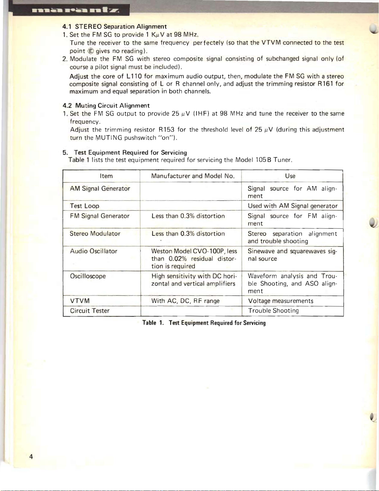
Table 1 lists the test
AM
Test
FM Signal Generator
I
Stereo Mod u
udio
A
Circuit
SG
the
trimming
the
MUTING
Equipment
Item
Signal Generator Signal
Loop
lator
Oscillator
I
Osc
ill
oscope
VTVM
Circuit
Tester
Alignment
output
to
resistor R153
pushswitch
Required
equipment
provide
for
Manufacturer
Less
Less
Weston Model CVOthan
tion
High sensitivity
zontal and vertical
With
25
/-lV
(lHF)
for
the threshold level
"on").
Servicing
required
than 0.3%
than 0.3 %
is
AC, DC, R F range Voltage measurements
0.02%
required
for
and Model No.
distortion
distortion
residual distor-
at
98
MHz and tune the receiver
of
25
/-lV
(during this
servicing the Model 105 B Tuner.
Use
source
ment
Used
with
AM
Signal source
ment
Stereo separation alignment
and
l00P,
with
DC
amplifiers
less
hori-
trouble
Sinewave and squarewaves
nal source
Waveform analysis and
ble Shooting, and ASO
ment
Trouble
shooting
Shooting
to
the
same
adjustment
for
Signal generator
for
align-
AM
FM align-
sig-
Trou-
align-
4
Table
1.
Test Equipment
Required
for
Servicing
Page 7

POINTER
Figure
1.
Dial
56
Stringing
5
Page 8

...
--
..
--
...
SOOl
~
~/A
~"",_C£-
Figure
2.
Front
Panel
wnod
Adjustments
..
• I ".
and
ion
Component
Locations
6
Figure
3.
Main
Chassis
Component
1
Locations
'-----
---
(Top
P400
l02
View)
Page 9

JO
3
LOOt
Figure
4.
J012
Rear
Panel
Adjustment
and
Component
locations
GOOt
ROOl
•
o
1 61
•
Figure
5.
Main
Chassis
Component
locations
(Bottom
View)
7
Page 10

...
--
..
--
...
~
Figure
6.
FM/AM
Tuner
Assembly
Pl00
Component
Locations
Figure
7.
A
sse
FM,
mbly
AM,
PlOO
Mono
and
Component
Muting
Locations
•
•
•
•
•
•
•
•
•
Switch
8
••
--:
=--
-"IVV\---.:.ee
Figure
_:--~'I/W1I,-.
8.
Power
P400
Component
Supply
------'
••
Assembly
Locations
Page 11

I'M
AM
LOCH
..
z
..
'"
<
HI02
Hr03"""
lOS
ti
II
0
HTl05361G
2SC536G
HlI!
•
HTl05361
2SC536E
nt:
H
E
113
ti1l4
H!l5.116.ll'9
H H 7
....
IZ5
,118
HD2001105
151555
TRANSISTOR
COf'HU':cTION
IBOTTOM
HIO
HIOZ_t·nI3
1-1401
O.ORAIN
S SOURCE
G
GATE
E;
EMITTER
VIEW)
fiflure
9.
Schematic
MOOI
COOl
Page 12

Page 13

PARTS
LIST
REF.
DESIG.
0103
01
0105
0106
0108
0427
0429
0431
0607
0609
0512
0513
0526
0527
0528
M007
0703
0821
J002
I
PlOD
Rl0l
Rl02
I
Rl03
Rl04
Rl05
Rl06
Rl07
Rl08
Rl09
Rll0
R
Rl12
Rl13
Rl14
Rl15
Rl16
Rl17
Rl18
Rl19
R120
R121
I
R122
R123
R124
R125
PART
284906340
A
284906301
282740101
04
282715801
281825905
284905301
285027340
B
257706302
257727301
285011201 Shaft
53110603E
54020601E
C
120200640
120225801 Ho
72080802A
285010341
D
281810301
285010301
281805301
IN1008030
E
284916040
284916001 Bracket
55060365S
YJ0400018
YD2886001
YD2849101
RT0510114
RT0556314
RT0510514
RT0510414
RT0510114
RT0510514
RT0510214
RT0510114
RT0510114
RT0510314
RT0510314
l1
1
RT0512214
RT0533314
RT0547114
RT0515114
RT0515114
RT0522214
RT0515214
RT0510114
RT0556214
Ri0512314
RT0510214
RT0510114
RT0515114
RT0533114
NO.
DESCRIPTION
Front
Panel Assembly
Es
cutcheon
Frame
Window
Bush
x 5
Cover
Fly Wheel Assembly
Escu
tcheon
Fly
Wheel
Hexagon Nu t
Flat Washer P
S
tri
ng
ok
Stri
ng
ointer
P
Pointer
Pointer
Cover
Lamp
Rear Pane
T.R. Riv
Jack
P.W.
Boar d,
P.W.
Board Assembly
RESISTORS
All
resistors
unless otherwise indicated.
lOOn
56Kn
lMn
100Kn
100n
lMn
1
Kn
loon
lOon
10Kn
10Kn
1.
2Kn
33Kn
470n
150n
150n
2.
2Kn
1.
5Kn
loon
5.6Kn
12Kn
lKn
loon
150n
330n
x2
Asse
mbl
Assembly
l Assembly
et x 2
Tuner
are ±5%
y
and '!.W,
I
I
REF.
DESIG.
R126
R127
R128
R129
.
R130
R131
R132
R133
Rl34
R135
R136
R137
Rl38
R139
R140
R141
R142
R143
R144
R145
R146
R147
R148
R149
R150
R151
R152
R153
R154
R155
R156
R157
R158
R159
R160
R161
R162
R163
Rl64
R165
R166
R167
R168
R169
R170
R171
Rl72
R173
R174
R175
R176
Rl77
R178
R179
R180
R181
R182
R183
R184
R185
R186
R187
PART
NO.
RT0533214
RT
0510214
RT0533214
RT0515314
RT0527214
RT0515114
RT0533114
RT0515114
RT0510114
RT0510414
'RT0515114
RT05822
RT0515314
RT0510214
RT0522114
RT0582114
RT0582114
RT0510114
RT0568214
RT0568214
RT0518314
RT
RT0522314
RT0582214
RT0515314
RT0510114
RT0533314
RA0104015
RT0522314
'
RT0522314
RT0547314
RT0533214
RT0510114
AT0518314
RT0510014
RA0103020
RT0547214
RT0515214
RC1033412
RT0568414
RT051
RT0568414
RT0510414
RT0543214
RT0543214
RT0510214
RT
RT0522414
RT0522414
RT051
RT0515214
RT0568214
RT0515314
RT0527214
RT0515214
RT0582314
RT0522114
RT0556214
RT0582314
RT0515314
RT0513314
RT0522214
14
0510314
0414
0510214
oj
14
3.
3Kn
lKn
3.3Kn
15Kn
2.
7Kn
150n
330n
150n
lOOn
100Kn
150n
8.2Kn
15Kn
lKn
220n
820n
820n
loon
6.
8Kn
6.
8Kn
18K
n
10Kn
22Kn
8.2Kn
15Kn
loon
33Kn
Trimming,
22Kn
22Kn
47Kn
3.
3Kn
lOOn
18K
n
10n
Trimming,
4.7Kn
1.
5Kn
330Kn ± 10
680Kn
100Kn
680Kn
100Kn
4.
3Kn
4.
3Kn
lKn
lKn
220Kn
220Kn
100n
1.5Kn
6.
8Kn
15Kn
2.7Kn
1.5Kn
82Kn
220n
5.
6Kn
82Kn
15Kn
13Kn
2.
2Kn
DESCRIPTION
100Kn
(B)
10Kn
(B)
%,
'h
I
W
I
13
Page 14

.....
--
..
--
...
~
RE F.
DESIG.
R188
R189
R190
R191
R192
R193
R194
Cl0l
Cl02
Cl03
Cl04
Cl 05
C
l06
Cl07
C10B
Cl09
Cll0
Cl
Cl12
Cl13
Cl14
C115
Cl16
Cl17
Cl18
Cl19
C120
C121
Cl22
C123
C124
C125
C126
C127
C128
C129
C130
C131
C132
C133
Cl34
C135
C136
C137
C138
C139
C140
C141
C142
C143
C144
C145
C146
C147
C148
C149
C150
C151 OF 161-0201
C152
C153
PART NO.
RT05472
RT0522214
RT0522314
RT0533214
RT0515214
RT0527414
RT0510414
CA3240007
001210001
OK1710201
OK
1820302
EM2240251
OK1820302
OK1820302
OK1840302
0012
10001 Ceramic,
001105001
ll
001530101
001615003
OK 1710201 Ceramic,
OK 1
840302
OK1820302
001102004
001615003
001520001
001207003
001525003
OK1820302
001650101
OK1840302
OK1820302
EA
1060169
OK1840302
OK1840302
001620001
EA
1060169
001610101
OK1820302
OK1840302
OK1820302
OK1820302
OK1820302
OK1840302
OK1840302
EA1060169
001650101
EA1060169
001620101
001620101
OK1840302
001610101
OK1820302
EA1050509
EA1050509
OFl722201
EA3350509
EA
1060169
EA
1060169
EA3360109
14
4.7K!1.
2.2K!1.
22K!1.
3.3K!1.
1.5K!1.
270K!1.
100K!1.
CAPACITORS
Variable,
Ceramic, 10PF ± 10%
Ce
ramic,
Ceramic,
Electroly,
Ceramic,
Ceramic,
Ceramic,
Ceramic,
Ceramic,
Ceramic, 15PF ± 10%
Ceramic,
Ceramic, 0.02,uF
Ceramic,
Ceramic,
Ceramic,
Ceramic, 7PF ±
Ceramic, 25PF ±
Ceramic,
Ceramic,
Ceramic,
Ceramic,
Electroly, 1O,uF,
Ceramic,
Ceramic,
Ceramic, 20PF ±
Electroly,
Ceramic, 10PF ± 10%
Ceramic,
Ceramic,
Ceramic,
Ceramic,
Ceramic,
Ceramic,
Ceramic,
El e
ctroly,
Ceramic, 500P F ± 1
Electroly,
Ceramic,
Ceramic,
Ceramic,
Ceramic,
Ceramic,
Electroly,
Electroly,
Film,
Electroly,
Elec
troly,
Film,
Electroly,
Electroly,
DESCRIPTION
AM-2,
FM-3,
O.OOl,uF ± 20%
0.02,uF
0.22,uF,
0.02,uF +100%,
0.02,u F +100%, -O"
O.04,uF
10PF ±
5PF ± 0.5PF
300PF ±
O.OOl,uF
O.D4,uF
2PF ± 0.5PF
15PF±10
20PF ±
0.02,uF +100%, -0%
500PF ± 1
D4,uF
O.
0.02,uF +100%,
O.D4,uF
0.04,uF
1
O,uF,
0.02,uF +100%,
O.D4,uF
0.02,uF
0.02,uF
0.02,uF +100%,
O.D4,uF
O.D4,uF
1
O,uF,
1
O,uF,
200PF ±
200PF
0.04,uF
100PF±10%
0.02,uF
l,uF,
l,uF,
0.0022,uF ± 20%
3.3,uF,
1
O,uF,
O.OOl,uF ± 10%
1
O,uF,
33,uF,
Gang
+100
%,
25V
+80
%,
10
%
5%
±20
%
+80%,
+100
%, -0%
%
5%
lPF
5%
0%
+80
%,
16V
+80%,
+80
%,
10"
'{'
16V
+80"/0,
+100
%,
+100
%, -0%
+80"'{',
+80%, -20%
16V
O"
'{'
16V
10
%
±10
%
+80
%,
+100
%, -0%
50V
50V
50V
16V
16V
10V
-0%
-O"
-20%
-20
-20%
-0%
-20%
-20%
-0
-20
-0%
-0
-20"
-20"
%
%
'{'
%
%
REF.
DESIG.
C154
C155
C156
C157
C158
C159
C160
C161
C162
C163
Cl64
C165
C166
'{'
'{'
'{'
C167
C168
C169
C170
C171
Cl72
C173
C174
C175
C176
Cl77
C178
C179
C180
C181
C182
C183
C184
C1
C186
C187
C188
Hl01
Hl02
Hl03
H1D4
Hl05
Hl06
Hl07
Hl08
Hl09
Hl10
H 111
Hl12
Hl13
H114
Hl
Hl16
Hl17
Hl18
Hl19
H120
H121
H122
H123
H124
H125
H126
PART
OF1627201
OF1627201
EA4740501
EA4740501
OFl647201
OFl647201
OF1533205
OF1533205
OF5582101
OF5582101
OF1618205
OF1618205
OF1615301
OF1615301
EA4740501
EA4740501
EA2270169
OF1768201
OFl722301
OF1740301 . Film,
OF6539101
001620001
OF1740301
EA476010Q
OK1840302
001530101
001620101
OFl647201
DFl64720
840302 Ceramic,
DK l
EA
85
15
4740501
DK
1840302
EA1050509
CTll00008
OK1710301
HF20D411 B F.E .T.,
HT306681C
HT309301C
HT309301C
HT309301C
HT309301C
HT309301C
HT309301C
HT309301C
HT305361G
HT305361
HT305361
HT309291C
HC1001703
H01000303
H01000303
H02001105
H02001105
H01000303
H01000303
H01000303
H01000303
H01000303
H01000303
HD1000303
H02000121
NO.
1
E Tran s
E
DESCRIPTION
Film,
Film,
Electroly,
Electroly,
Film,
Film,
Fi
lm,
Film,
Film,
Film,
Film,
Film,
Film,
Film,
Electroly,
Electroly,
Electroly,
Film,
Film,
Film,
Ceramic, 20PF ± 10%
Film,
Electroly,
Ceramic,
Ceramic,
Ceramic,
Film,
Film,
Electroly,
Ceramic,
Elec
troly,
Trimming,
Ceramic,
SEMICONDUCTORS
Transis
Transistor,
Transistor , 2SC930 (C)
Transistor, 2SC930 (C)
Transis
Tr
ansistor,
Trans
Tran sistor, 2SC930 (C)
Transi s
Tran sistor, 2SC536 (E)
Transis
I.C.,
Oiode,
Oiode,
Oiod
e,
Oiode,
Oiod e,
Diode,
Oiode,
Diode,
Oiode,
Oiode,
Oiode,
Oiode,
0.0027,uF ± 10%
0.0027,uF ± 10%
OA7,uF,
OA7,uF,
0.0D47,uF ±
0.0047,uF ± 10%
0.0033,u F ±
0.0033,uF ± 5%
820PF ±
820PF ± 5%
0.OO18,uF ± 10%
0.0018,uF ± 10%
0.015,uF ± 10%
0.015,uF ± 10%
OA
OA
220,uF,
0.0068,uF ± 20%
0.022,uF ± 20%
O.D4,u
390PF ± 5%
0.04,uF ± 20%
47,uF,
0.04,uF
300PF ± 5%
200PF ± 10%
0.0D47,uF ± 10%
0.0047,uF ± 10%
O.D4,uF
OA7,uF,
O.
l,uF,
10PF,
O.Ol,uF ± 20%
2SK41 (E)
tor,
2SC668 (C)
2SC930 (C)
tor,
2SC930 (C)
2SC930(C)
istor,
2SC930 (C)
tor,
2SC536 (G)
istor,
2SC536 (E)
tor
, 2SC929 (C)
LA3310
lS188FM2
lS188FM2
lS1555
lS1555
lS188FM2
lS188FM2
1
lSl88FM2
lS188FM2
lS188FM2
lS188FM2
lS2473
7,uF
,
7,uF,
F ± 20%
+80"
+80%,
D4,uF
+80
S188FM2
-C
5%
50V
50V
10"
5%
50V
50V
16V
10V
'{' , -20"
50V
%,
50V
NPO
'{'
-20%
-20
'{'
%
I
14
Page 15

REF.
DESIG
. .
PART
NO.
DESCRIPTION
REF.
I
DESIG.
PART
NO.
DESCRIPTION
I
Jl0l
Jl03
I
J126
0906
0907
0908
1110
P400
R401
R402
R403
R404
C401
C402
C403
C404
C405
C406
C407
C408
H401
H402
H403
H404
H405
J401
I
J409
YP10ool13
YP10ool13
282110901
288610904
285010902
62031650W
YD2849004
ZZ
2849
004
GJ1025
102
GJl
0251
RT0533314
RT0533314
DK
DK1810351
EA3370509
EA4770109
EA3370359
EA1070160
EA2270169
DK1840301
HT311751
HD2001003
HD2001oo3
HD2001003
HD3002109
YPloo0099
02
181 0351
MISCELLANEOUS
Plug
Plug
Shield
Shield
Shield
Lug
PW
. Board,
PW
. Board A sse
RESISTORS
250n
± 10%,
250n
± 10%,
33Kn
±5%.
33Kn±
CAPACITORS
Ceramic,
Ceramic,
Electroly
Electroly,
Electroly,
Electroly,
Electroly,
Ceramic,
SEMICONDUCTORS
E
Transistor,
Diode,
Diode,
Diode, DS130
Diode,
MISCELLANEOUS
Plug
Power
mbly
5%,
O.Ol,uF +100%,
O.Ol,uF +100%, -0%,
,
330,uF,
470,uF,
330,uF,
1
OO,uF,
220,uF,
O.04,uF
+100
2SCl175
(YD)
DS130
(YD)
DS130
(YD)
BZ140
2W
2W
YO
W
YOW
50V
10V
35V
16V
16V
(E)
%,
-0"10,
-0"10
500V
500\1
P300
R301
R302
R303
R304
R305
R306
C301
S301
J301
J302
Sool
MOOl
COOl
0417
1438
1439
0501
0503
0505
0502
1436
1437
0414
0631
J005
J006
J007
J008
M002
MOO3
MOO4
M005
1537
1538
YD2849OO3
ZZ2849703
RT0510214
RT0510214
RT0518314
RT0518314
GT0515212
RT0539214
EA4760169
SP0604oo3
YP.l00oo99
YP1000099
SP0301001
IM1104208
EA1070109
285011801
285012003
289105305
285016009
263711203
257726201
285016008
263711203
257726201
281827101
51570306B
YJ0800013
YJ0800013
YJ0800013
YJ0800013
IN1008007
IN1008007
IN1008007
IN1008007
289110106
51570315B
PW
. Board
P.
W.
Board Assembly
Resistor,
Resistor,
Resistor,
Resistor,
Resistor,
Resistor,
Electroly
Push
Plug
Plug
Push
DC Meter, Signal
Electroly
Spacer
Insulator
Cover
Bracket
Shaft
Pulley
Bracket
Shaft
Pu
lley
Holder
P.H.
Tapt
Socket
Socket
Socket
Socket
Lamp
Lamp
Lamp
Lamp
Support
P.H .
Tapt
Cap.,
Switch,
Switch
Cap.,
Screw x 4
Screw
lKn
lKn
18Kn
'
18Kn
1.5Kn
3.9Kn
Band Selector
±5%,
±5%,
±5%,
± 5%,
±5%,
±5%,
47}..LF,
loo,uF,
YOW
YOW
YOW
YOW
Y.W
YOW
16V
10V
0403
0408
0409
0410
0412
0421
0422
0507
0611
0615
0618
0621
0623
0625
0626
282716050
285020101
285016003
285016004
285012201
257710602
141511801
285016051
51040306A
51100306A
51100306A
511oo306A
51100306A
51100306A
51100306A
Bracket K
Partitioner
Bracket
Bracket
Sticker
Bearing
Spacer
Bracket K
F.
H.M
. Screw x 2
B.H.M . Screw
B.H.M. Screw
B.H.M. Screw
B.H.M. Screw
B.H .M. Screw
B.H.M . Screw
x4
x4
x6
x2
x3
R003
0415
0518
1536
P200
M201
M202
M203
J201
I
J205
RC1002012
282716003
282710701
51570306B
I
YD2849002
ZZ2849OO2
IN1006301
IN1006301
IN1006301
YP1000099
I
Resistor,
Bracket
Sheet
P.H.
Tapt
P.w
. Board
P.W. Board Assembly
lamp,
Lamp,
Lamp, 6.
Plug
2n
± 10%,
Screw x 2
6.
3V,
6.
3V.
3V,
40mA
40mA
40mA
Y.
W
15
Page 16

......
__
....
a';"JJL
REF.
DESIG.
R002
0413
0619
0630
0418
0718
0814
0819
0826
0827
0832
0833
JOOl
J003
JOO4
J010
WOOl
GOOl
FOOl
J011
J012
L003
LOOl
0710
0714
0806
0807
0808
0810
0811
ROOl
1133
0903
0904
0915
2236
W002
W003
PART
NO.
RC1018012
282727401
51570306B
51570305B
282705101 Guide
145525903
51100306S
54050400R
51100308S
53110303E
5'1100308S B.H.M. Screw
53110303E
YJ0800012
YT0104004
YT0202007
YT010l003
YC0240010
BF1040001 Printed
FSl
01
0008
YL0102003
YT0201006
LCl154004
LFl120024
257816052
281927103
51100308S
54050300R
53110303E
51100310S
53110303E
GT0522512
62031650W
282715901
71101569M
51064019A
138200503
YW2849001 Wire Material
YX2849001
Resistor,
Reflector
P.H.
P.H.
Bush x 2
B.H .M. Screw
T.
l.
B.H.M. Screw
Hexagon
Hexagon
Socket, Fuse Holder
Terminal,
Terminal,
Terminal,
AC
Fuse,
Terminal
Terminal,
Choke
Ant.
Bracket K
Holder
B.H.M. Screw
T.L. Washer OR
Hexagon
B.H .M. Screw
Hexagon
Resistor, 2.
Lug
Drum
Spring
Screw
Clamper
Wire Material
DESCRIPTION
Tapt
Screw x 2
Tapt
Screw x 4
Washer OR
Nut
Nut
Cord
Compo
Coil,
Coil
Nut
Nut
x2
x3
18n
± 10%,
x3
x 2
x2
x4
x4
Ant.
Output
Ground
.,
lA
(ULl
Quadradial
150f.LH
x2
x2
x 2
x2
x 2
2Mn ±5%,
O.lf.LF
+
'hW
120n
'hW
REF.
DESIG.
1033
1103
1104
1108
1113
1122
1124 51100306S B.H.M. Screw
1126
1127
1131
1132
1135
1-117
2836
2837
0112
0118
0119
0120
0202
0203
0207
0211 257886101
0212
0213
0214
0219
0220
0224
0225
3037
0302
0304
0306
0432
0433
3038
0532
0604
0634
0635
PART
NO.
138200503
51570408B
54040402N
51570306B
51570306B
51570306B
51570306B
54050300R
51570306B
54050300R
54050300R
53110303E
51570306B
54050300R
281815401
284925701
257711803
282825702
284926501
284926502
284926506
257886102
257886103
250626506
951091101 Label,
282186102
951110103
245786104
951091102
51122608E
51100406S
51480406S
285011202
284912001
288686101 Label
282626901
54040402N
51100304S
56382540G
Clamper
P.H .
Spri
P.H.
P.H.
P.H .
P.
H.
T.l.
P.H . Tapt Screw
T.l.
T.l.
Hexagon
P.H.
T.L.
Knob
Lid,
Spacer
Lid
Indicator,
Indicator,
Indicator
Label,
Label,
Label,
For
Indicator,
Label,
Label,
Label,
Label,
T.H.M
B.H.M. Screw
B.H.M.
Shaft
Insulator
Protector
Spring Washer
B.H.M. Screw
Eyelet
Tapt
ng
Washer
Tapt
Tapt
Tapt
Tapt
Washer OR x 2
Washer OR
Washer OR
Tapt
Washer OR
x 5
Do
U.S.A.
. Screw
Screw F
DESCRIPTION
x4
Screw x 2
x2
Screw x 6
Screw x 3
Screw x 8
x6
Screw x 7
Nut
Screw
Caution
Marking
Not
Use
x4
x8
4,
x
x 2
For
For
For
For
on
as
For
For
For
For
For
For
x 3,
UL
Not
Remove Cover, For U.S.A.
See
Do
LL
NO,
Caution,
UL,
CSA,
U.S.A.
U.S.
A.
U.S.A.
CANADA
Bottom,
Handle
CANADA
CANADA
U.S.A.
CANADA
U.S.A.
U.S.A.
I
I
I
I
16
PZOl
MZOl
MZ02
JZOl
JZ02
0521
0523
0423
0603
2737
0605
0121
0310
1026
YD2891007
ZZ2891
007
IN1006302
IN1006302
YP1000113
YP1000113
284930201
282705302
281810650
516404120
54040402N
53l10403E
275905701
51490410S
285010502
P.
W.
Board
P.W
. Board Assembly
Lamp
Lamp
Plug
Plug
Dial
Cover
Bearing K
Set Screw C.
Spring Washer
Hexagon
Leg
B.H .M. Screw F.S.
Chassis
P.
Nut
0613
0614
0824
3137
3141
3142
1202
1209
3236
1217
1219
1221
1302
1303
1305
1306
4,
x
For
For
U.S.A.
U.S.A.
x
4,
1308
1309
1312
1313
51100306A
54050300R
51100306S B.H.M. Screw
288506450
52010420A
54080400R
284985101
284985601
288785108
288585107
281885104
257785450
284980105
284980106
284980102
284980112
289180301
288280303
901383033
901433533 1Polyethylen
B.H.M . Screw
T.l.
Washer OR
Case
K,
H. Head
T.l. Washer
Instructions
Schematic Diagram
Instructions
Instructions
Instructions
Guarantee Card K
Packing
Packing
Pack
Pack
Partitioner
Partitioner
Polyethylen
ing
ing
Bolt
Case,
Case,
Case,
Case,
RR
x 2,
x 2,
Bag,
Bag,
x 2
x 2
x2
x 4,
x4
For
For
For
For
For
For
For
For
For
For
CANADA
CANADA
I
U.S.A.
U.S.A.
CANADA
CANADA
U.S.A.
CANADA
U.S.A.
CANADA
I
Page 17

REF.
DESIG
PART
.
NO.
DESC
RIPT ION
1314
1317
1319
1320
1323
1324
1332
1333
1334
901302501
102980401
273182101
281905601
952281501
952301512
ZA0200007
Z00200010
Z00120006
Polyethy
Sleeve
Silicagel
Buffer
Serial No Card
er
ial
No
S
Ext.
Antenna
Connective
Connective
I
len
Card
Bag
Cord
Cord
x 2
x2
x4,
x
4, For
For
U.S.A .
CANADA
17
Page 18

..............
"1'.
TECHNICAL
FM
SECTION
Tuning Frequency
I H FM Usable
IHFMSelectivity
SPECIFICATIONS
Range
Sensitivity.
...............................................
. . . . . . . . . . . . . . . . . . . . . . . . . . . . . . . . . . . . . . . . . . . . . . . . . . . . . . . .
.............
,.,
.........
.. . ..
..
.... . ... . .. . ..
....
. .
.
.....
...
88 - 108MHz
......
.. 3,011
Capture Ratio . . . . . . . . . . . . . . . . . . . . . . . . . . . . . . . . . . . . . . . . . . . . . . . . . . . . . . . . . . . . . . . . . . .
Impage Rejection Ratio at 1 06MHz . . . . . . . . . . . . . . . . . . . . . . . . . . . . . . . . . . . . . . . . . . . . . . . . .
to
Signal
Signal
Total Harmonic
Toral Harmonic
Frequency Response (ref.
Stereo Separation
Noise Ratio (Mono) . . . . . . . . . . . . . . . . . . . . . . . . . . . . . . . . . . . . . . . . . . . . . . . . . . . . . 65dB
to
Noise Ratio (Stereo) . . . . . . . . . . . . . . . . . . . . . . . . . . . . . . . . . . . . . . . . . . . . . . . . . . . . . 55dB
Distortion
Distortion
at
1 KHz
(Mono) . . . . . . . . . . . . . . . . . . . . . . . . . . . . . . . . . . . . . . . . . . . . . . . . . 0.5%
(Stereo) . . .
7511
sec.
de-emphasis)
......................
...
.......
..
.
. . . .
..
....
. . .
.....
...............
............
.....
.
.....
..
............
. .
...
... ±2dB
. . ..........
..
..
.....
, 30Hz·15K
AM SECTION
Tuning Frequency
Usable Sensitivity
Selectivity
Image Rejection Ratio at
to
Signal
Noise Ratio
Frequency Response,
Total Harmonic
Range
..............
.... . .............
1400KHz
............
-3dB
Distortion
....................
.
.........................
.
...........
...
...
..
.........
down
..........
....
.....
. . . .
. . . .
......
...
...
...
........
....
..
. .
..
..
..
... . .....
....
......
.......
_ . . . . . . . . . . . . . . . . . . . .
.....
. . . . . . .
. .
.....
....
. .
...
. . . . . . . . . . . . . . . . . . . . . . . . . . . . . . . . . . . . . . . .
. . .
.........
..
...........
.. . ..
... . .....
...............
........
. . . .
.. ......
540-1605 K
..
..
....
..
..
50 Hz-3.3
... ...
V
4
8dB
3dB
50dB
0.
8%
Hz
40dB
Hz
2511
V
. 20dB
40dB
45dB
KHz
..
1%
GENERAL
Power Requirements
Power Consu
Dimensions -
mption
Panel
Panel
-
Width
Height
-Depth
Weight -
Unit
along
- Packed
* These specifications and
............
.....
...
...........
...........
...................
for
Shipment
exterior
..........
...
...
designs
. .
....
..
...........
..
.....
..
.........
may
be
changed
..
....
.
... . ........
............
........
.... . .. . ........
__
.
.....
..
....
. .
.........
....
..
. _
.....
.
...
. .
... . ...........
for
improvement
..............
...
..
..
...
.. _...
....
...........
. . .
with
out
..
. . .
..
..
...
_
..
..
....
.....
..
14-11/
. _ . . . . . . . . . 4
. . .
..
. 11-1/
. .
...
..
. _
.....
advance notice.
.. _... . 17.6Ibs-SKg
..
. . .
..
120 V AC
50
...
. . . _ 15 Watts
64"-
23/
32"
-120
32"-2S0rnm
. 12.1I
bs-5.5Kg
to 60Hz
360
mm
mm
18
Page 19

~
7l'
-iii
-
MARANTZ
A
WHOllY-OWNED
CO.,
INC.·
SUBSIDIARY OF
P.O.
BOX
99·
•
SUPERSCOPE
SUN
INC.
VALLEY,
, SUN
CALIFORNIA·
VAllEY
, CALIFORNIA 91352
91352
28498550
4-0
 Loading...