Page 1
µ
µ
PSD
PSD
It’s All You Need.
Feb 2003 www.st.com/micropsd
1
Page 2
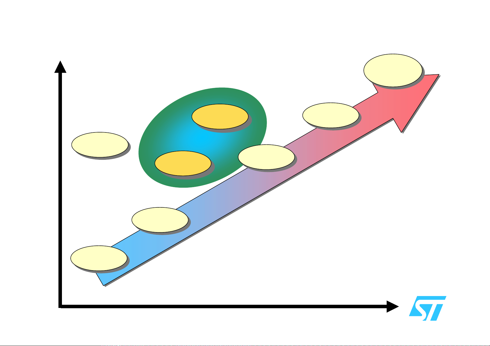
ST’s New 8051--
ST’s New 8051
!
!
W
W
E
N
N
E
Q303
Q303
µPSD
Turbo
Performance
8051 World
ST5
NOW
NOW
8051 World
µPSD
-
-
-
8
8
8
ST7
m
o
C
m
S
t
s
y
ST6
S
i
m
p
F
u
i
d
e
M
l
o
r
t
n
o
C
e
l
n
u
s
n
o
i
t
c
based MCU Family
based MCU Family
ST40 &
STPC
t
t
t
i
i
i
b
b
b
-
-
-
2
2
2
3
3
3
r
o
f
r
e
S
e
t
s
y
)
.
P
h
g
i
H
t
s
n
,
n
a
n
h
C
…
l
e
s
b
b
b
e
p
m
ST10
t
t
t
i
i
i
b
b
b
-
-
-
6
6
6
1
1
ST9
t
t
t
i
i
i
y
t
i
x
e
l
s
c
i
l
p
A
p
r
M
(
o
m
e
e
t
x
E
o
i
t
a
O
,
I
/
y
1
e
m
i
T
-
l
a
e
s
q
m
g
n
i
s
e
m
e
r
i
u
t
a
i
n
o
i
n
u
c
R
e
v
i
s
P
C
r
R
o
o
c
m
e
e
n
n
,
s
m
m
e
c
n
a
s
www.st.com/micropsd
2
Page 3
What is
What is
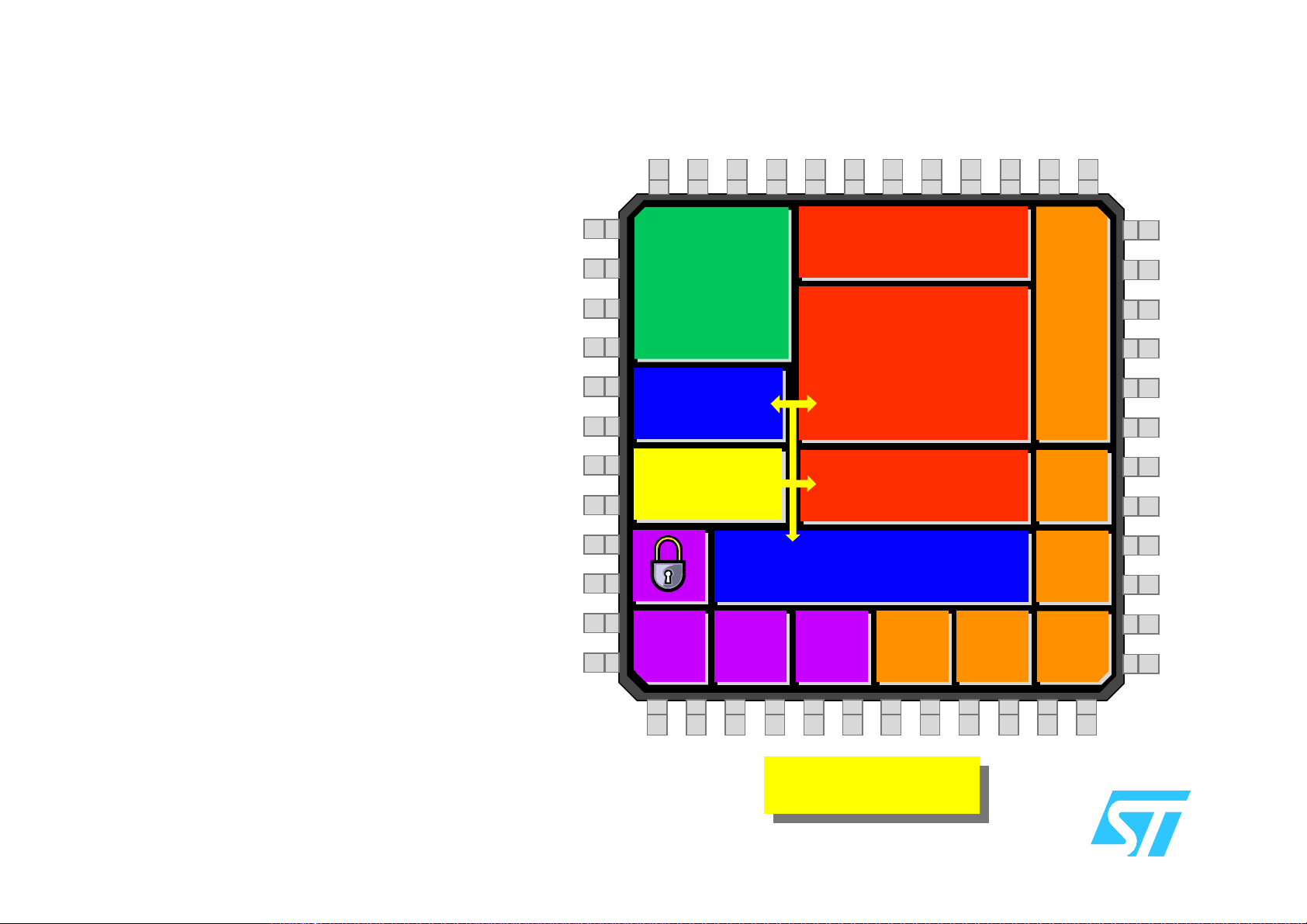
• Standard 8032 MCU Core
– (3) 16 bit timers
µ
PSD
µ
PSD
?
?
– (2) Ext Interrupts
• Large Dual Bank Flash
• Large SRAM
• Programmable Logic
• USB, Dual UARTs, I2C
• PWM, ADC, DDC
• Many I/O
• Built-in Supervisor
8032
8032
8032
8032
CORE:
CORE:
CORE:
CORE:
w/UART&
w/UART&
w/UART&
w/UART&
WDOG TMR
WDOG TMR
WDOG TMR
WDOG TMR
DECODE &
DECODE &
DECODE &
DECODE &
MEM MNGR
MEM MNGR
MEM MNG R
MEM MNG R
JTAG ISP
JTAG ISP
JTAG ISP
JTAG ISP
PROGRAMMABLE
PROGRAMMABLE
PROGRAMMABLE
PROGRAMMABLE
Vcc
Vcc
Vcc
PWR
PWR
PWR
PWR
MNG
MNG
MNG
MNG
Vcc
MON
MON
MON
MON
2K, 8K, or
2K, 8K, or
2K, 8K, or
2K, 8K, or
32K Byte SRAM
32K Byte SRAM
32K Byte SRAM
32K Byte SRAM
64K, 128K, or
64K, 128K, or
64K, 128K, or
64K, 128K, or
256K Byte
256K Byte
256K Byte
256K Byte
MAIN FLASH
MAIN FLASH
MAIN FLASH
MAIN FLASH
16K or 32K Byte
16K or 32K Byte
16K or 32K Byte
16K or 32K Byte
nd
nd
nd
nd
FLASH
FLASH
FLASH
FLASH
DDC
DDC
DDC
DDC
LOGIC
LOGIC
LOGIC
LOGIC
ADC
ADC
ADC
ADC
2
2
2
2
I2C
I2C
I2C
I2C
I/O
I/O
I/O
I/O
PWM
PWM
PWM
PWM
USB
USB
USB
USB
1.1
1.1
1.1
1.1
nd
nd
nd
nd
2
2
2
2
UART
UART
UART
UART
• ISP
– In-System Programming
• IAP
– In-Application Programming
www.st.com/micropsd
Just add power
Just add power
and crystal!
and crystal!
3
Page 4

What makes
What makes
• PSD Architecture … enhances capability of 8051
– PSD = Programmable System Device
– Dual bank Flash Memory … Superior IAP
– Memory Management … Seamless paging and memory placement
– Programmable Logic … Consolidate external logic chips
– JTAG ISP … perfect for lab and manufacturing
• Some µPSDs have Big Memory up to 288K bytes…
When is larger Flash and SRAM needed?
– The use of C language
µ
PSD
µ
PSD
different?
different?
– Elaborate user interfaces … menus, graphics, screens
– Multiple languages and fonts, data tables
– Faster data transfers
– Data recording
• Low Cost
– Save $ compared to other 8051 and 8-bit MCU devices with
www.st.com/micropsd
larger SRAM and Flash Memories
4
Page 5

Unique
Unique
• Excellent Memory Management
• Flexible Memory Allocation
• Remote Field Updates
• JTAG In System Programming
µ
PSD
µ
PSD
features
features
www.st.com/micropsd
• Programmable Logic
PSD
PSD
Architecture !!!
Architecture !!!
5
Page 6
Excellent Memory Management
Excellent Memory Management
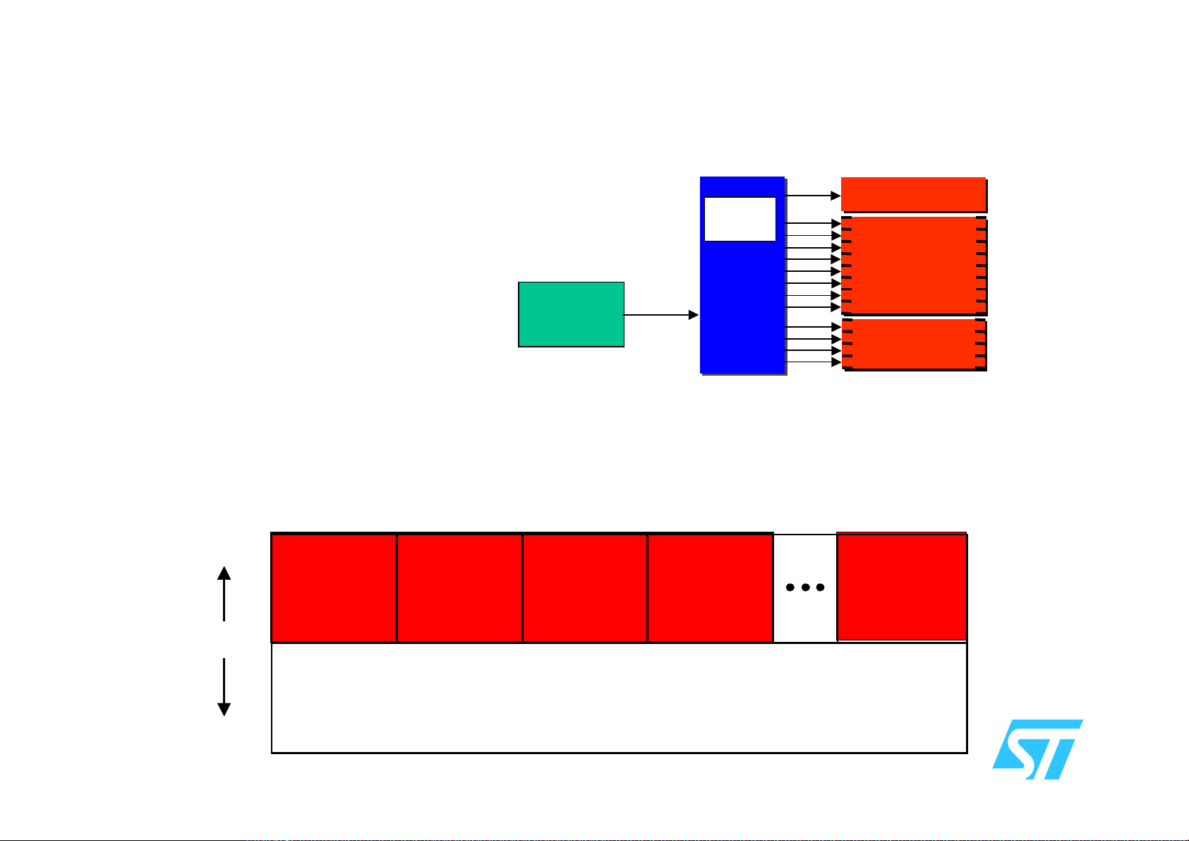
• Built-in Address Decoding PLD
– Map any µPSD memory sector to any address
– Easily convert existing 8051 designs into µPSD
– Total memory mapping flexibility for new designs
8032
8032
8032
MCU
MCU
MCU
• Memory Paging is Easy using Decode PLD
– Break traditional 8051 64K Byte address limit imposed by only 16 address lines
– 8-bit page register is built into Decode PLD … it’s like having 8 more address lines
– Paging (or banking) is directly supported by most 8051 C compilers
FFFF
Page 0
Page 0
Page 1
Page 1
Page 2
Page 2
Address
Page 3
Page 3
Page
Register
DECODE
DECODE
DECODE
PLD
PLD
PLD
Sector
Selects
Sector
Selects
SRAM
SRAM
SRAM
MAIN FLASH
MAIN FLASH
MAIN FLASH
MA I N FLAS H
MA I N FLAS H
MA I N FLAS H
MAIN FLASH
MAIN FLASH
MAIN FLASH
nd
nd
nd
nd
nd
nd
FLASH
FLASH
FLASH
2
2
2
FLASH
FLASH
FLASH
2
2
2
2ndFLASH
2ndFLASH
2ndFLASH
Page 7
Page 7
1
Sector
8
8
Sectors
Sectors
4
4
Sectors
Sectors
64K
0000
www.st.com/micropsd
32K Main
32K Main
Flash
Flash
32K Main
32K Main
Flash
Flash
Map here: SRAM, 2ndFlash, I/O, etc
32K Main
32K Main
Flash
Flash
32K Main
32K Main
Flash
Flash
Common to All Pages
32K Main
32K Main
Flash
Flash
6
Page 7
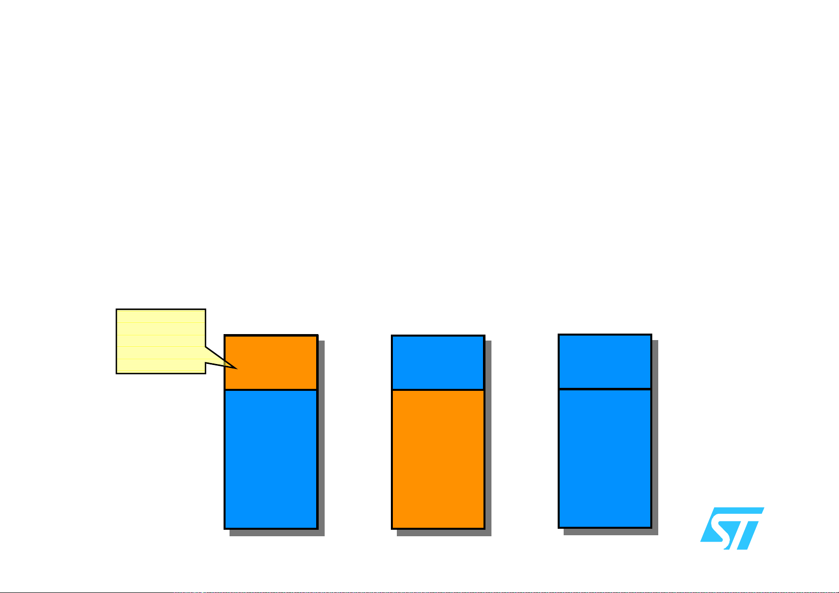
Flexible Memory Allocation
Flexible Memory Allocation
• 8051 Architecture uses a separate address space for code and for data
• Allocate dual banks of Flash to meet A pplicat ion De mands
– The Decode PLD controls where Flash memory resides
• You decide how to split the Flash memory
Can use
EEPROM
Emulation
Big Code
(complex
algorithms)
nd
nd
nd
FLASH
2
FLASH
2
FLASH
2
DATA
DATA
DATA
MAIN FLASH
MAIN FLASH
MAIN FLASH
CODE
CODE
CODE
-OR -
Big Data
(printers, big
GUI, tables)
nd
nd
nd
FLASH
2
FLASH
2
FLASH
2
CODE
CODE
CODE
MAIN FLASH
MAIN FLASH
MAIN FLASH
DATA
DATA
DATA
-OR -
All Code
(like typical
flash 8051s)
nd
nd
nd
FLASH
2
FLASH
2
FLASH
2
CODE
CODE
CODE
MAIN FLASH
MAIN FLASH
MAIN FLASH
CODE
CODE
CODE
www.st.com/micropsd
7
Page 8
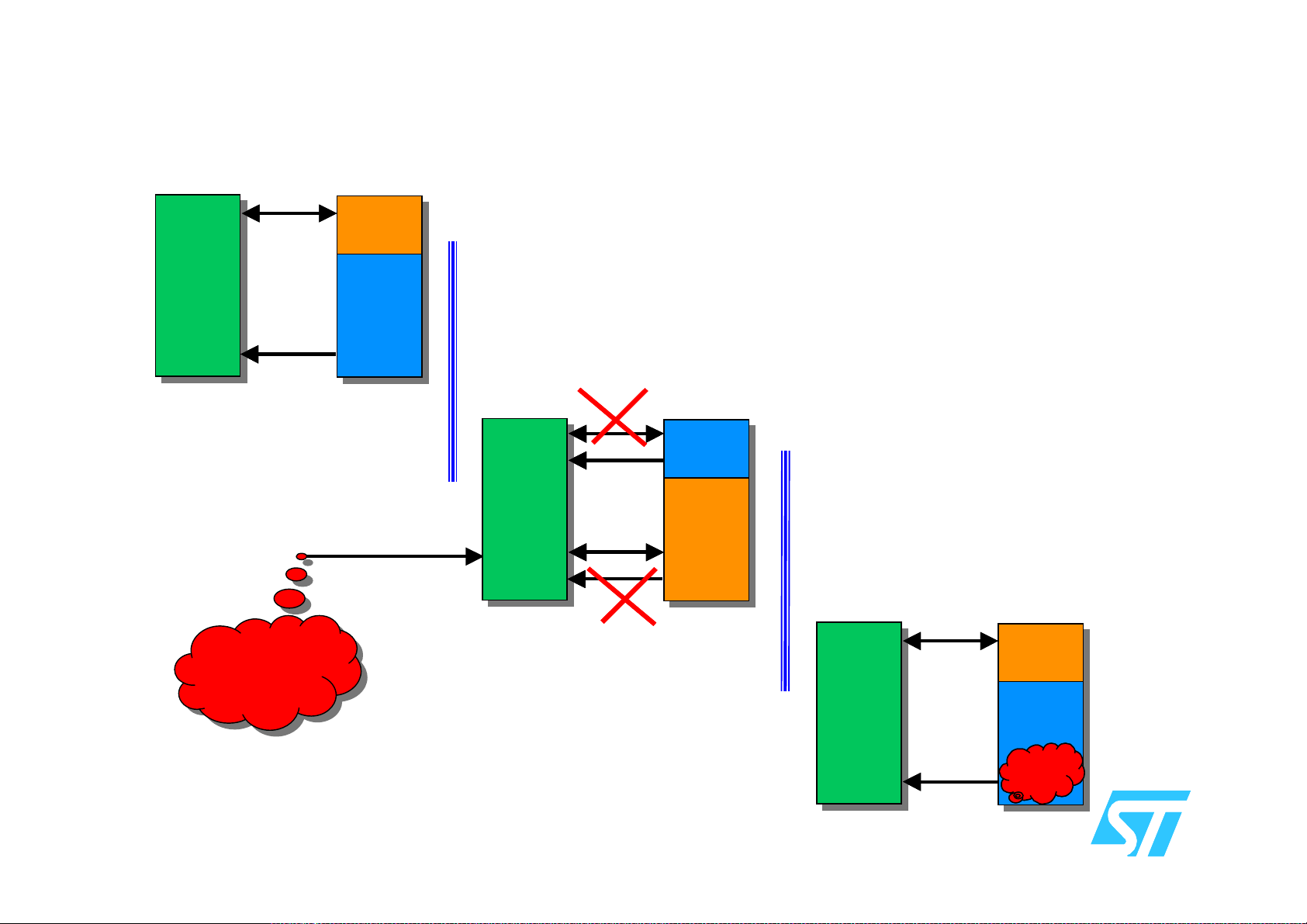
Remote Field Updates with IAP
Remote Field Updates with IAP
1. Before IAP
READ &
READ &
WRITE
WRITE
8032
8032
8032
8032
MCU
MCU
MCU
MCU
READ
READ
READ
ONLY
ONLY
ONLY
• MCU reading program
from Main Flash
Updated
Updated
Program
Program
nd
nd
nd
nd
2
2
Flash
Flash
2
2
Flash
Flash
DATA
DATA
DATA
DATA
MAIN
MAIN
MAIN
MAIN
FLASH
FLASH
FLASH
FLASH
OLD
OLD
OLD
OLD
CODE
CODE
CODE
CODE
USB, UART,
2
I
C, Modem…
• 8051s typically cannot write to “code” space
– Special µPSD register eliminates this limitation
• Typical Flash memory cannot be read and written
at the same time
– Dual Banks of Flash eliminate this limitation
– Read program from one bank while writing to the other bank
2. During IAP
READ &
READ &
READ &
WRITE
WRITE
WRITE
READ
READ
READ
ONLY
ONLY
8032
8032
8032
8032
MCU
MCU
MCU
MCU
ONLY
READ &
READ &
READ &
WRITE
WRITE
WRITE
READ
READ
READ
ONLY
ONLY
ONLY
• Special Register temporarily reclassifies Main Flash as Data
• MCU now reads IAP program
from 2ndFlash while receiving
bytes of new program from
USB, UART, Modem, I2C, etc.
and writes the new program to
Main Flash
nd
nd
nd
nd
Flash
Flash
2
2
Flash
Flash
2
2
CODE
CODE
CODE
CODE
MAIN
MAIN
MAIN
MAIN
FLASH
FLASH
FLASH
FLASH
TREAT
TREAT
TREAT
TREAT
AS DATA
AS DATA
AS DATA
AS DATA
• Special Register classifies
Main Flash as Code again
• MCU now reading new
program from Main Fla sh
3. After IAP
READ &
READ &
WRITE
8032
8032
8032
8032
MCU
MCU
MCU
MCU
WRITE
READ
READ
READ
ONLY
ONLY
ONLY
nd
nd
nd
nd
Flash
Flash
2
2
Flash
Flash
2
2
DATA
DATA
DATA
DATA
MAIN
MAIN
MAIN
MAIN
FLASH
FLASH
FLASH
FLASH
NEW
NEW
NEW
NEW
NEW
NEW
CODE
CODE
CODE
CODE
CODE
CODE
www.st.com/micropsd
8
Page 9
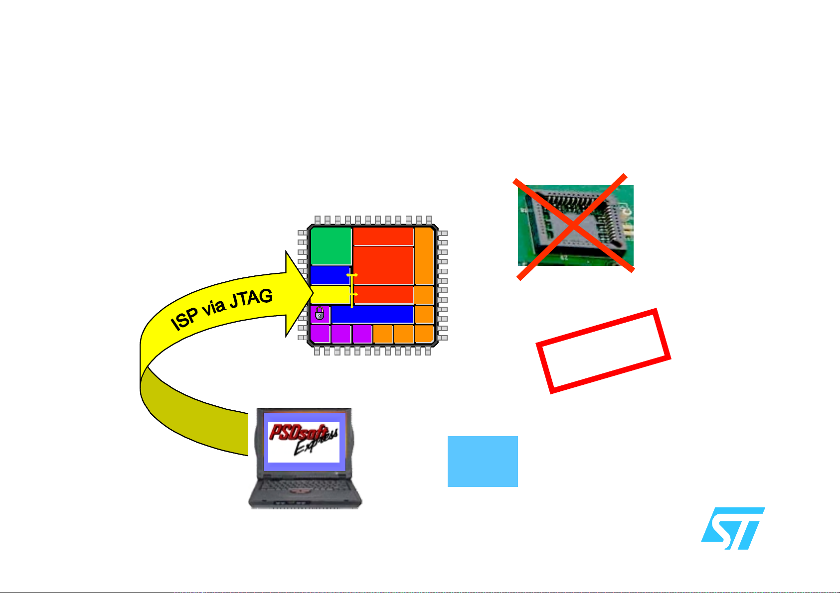
In--
In
• Program blank device, no interaction of 8032 MCU required
• Entire chip programs in 10-25 seconds
• JTAG serial connection is industry standard
• Speedy lab development and manufacturing
System Programming (ISP)
System Programming (ISP)
µ
PSD
µ
PSD
µ
PSD
µ
PSD
g
n
E
a
h
C
n
No soc kets or
pre-programmed
parts needed
g
n
i
r
e
e
n
i
O
e
g
r
e
d
r
Last minute
www.st.com/micropsd
JIT
changes are
OK
Just-In-Time
Inventory
Management
9
Page 10

Programmable Logic
Programmable Logic
• Built-in 16 MacroCell PLD for General Purpose Logic
• Similar to standard 22V10 architecture
PAL
• Eliminate small PLDs, PALs, 74XXX series discrete logic
• Easy Point-and-Click PLD configuration with PSDsoft Express
• Build:
– Glue logic
– State-machines
– Shifters
– Counters
– Chip-selects for extern al device s
– Keypad interfaces
Easy interface to external devices
PLD
74XXX
– Delay generators
– Clock dividers
– Decoders
– Multiplexers
www.st.com/micropsd
State 3
State 0
State 1
State 2
10
Page 11

A Unique Combination
A Unique Combination
• ST is the only large manufacturer that can bring:
- so much memory
- so many perip herals
- and programmable logic
In a cost effective device
• Excellent Flexibility to adapt designs and
grow wi th future product requirements
• Versatile, easy to use Programmable Logic
16 macrocells today, 32 coming in 2003
• 1 and 2Mbits Flash today …
4Mbits coming in 2003
www.st.com/micropsd
11
Page 12

Consolidate Devices
Consolidate Devices
• What common devices can uPSD eliminate from
your circuit board?
Sockets – not needed using J T AG ISP
Glue-logic chips – Use on-chip PLD
EEPROM chip – Emulate EEPROM using the second Flash memory
Supervisor chip – Low Vcc Detect and Watchdog included!
www.st.com/micropsd
12
Page 13

Broad Variety of Connectio ns
Broad Variety of Connectio ns
8032
8032
CORE
CORE
w/UART
w/UART
& WDOG
& WDOG
DECODE &
DECODE &
MEM MNGR
MEM MNGR
JTAG ISP
JTAG ISP
Vcc
PWR
PWR
PWR
PWR
MNG
MNG
MNG
MNG
Vcc
MON
MON
SRAM
SRAM
MAIN FLASH
MAIN FLASH
nd
nd
2
FLASH
2
FLASH
PROGRAMMABLE
PROGRAMMABLE
LOGIC
LOGIC
ADC
ADC
ADC
ADC
DDC
DDC
DDC
DDC
I2C
I2C
I2C
I2C
I/O
I/O
PWM
PWM
USB
USB
1.1
1.1
nd
nd
nd
nd
2
2
2
2
UART
UART
UART
UART
Keypads, Displays, LEDs, Relays,
Contol Panels, Sensors, Acuators
Glue Logic, Clock Dividers, State
Machine Sequencers, Simple
Counters, Shifters, Chip-Selects
Motor Control, Brightness Control, Position
Control, Simple DAC, Tone Generation
Widely used serial connection bus
supporting plug-and-play operation.
USB 1.1 Peripheral, 1.5Mbps, Control
Endpoint 0 and Intr Endpoi nts 1 and 2
Reduce PLD
Current for
Battery
Operation
www.st.com/micropsd
Connect Modems, Terminals, Displays, GPS Unit, Debug
Connect Displays, Communication Chips, Many Industry Peripherals
Data Display Chan for LCD Projector (DDC1, DDC2B)
Monitor Environment, Data Acquisition, Closed-Loop Control Feedback
13
Page 14

Development Support
Development Support
• µPSD C Compiler, Simulator, De bugger, Monitor
– Supported by Keil Software, #1 vendor for 8051 architecture
– Excellent UART ISD51 background debugger for breakpoints,
single-step, display memory and registers, etc.
$149 USD
– Standard 8051 compilers from other vendors are also
completely compatible with µPSD.
• DK3200 development board from ST, US$149
– Everything needed: hardware, software, JTAG programmer
– Firmware driv ers, exam pl e code, and U S B dem onst ratio n
TM
– Windows
– See Application Note AN1560 for guide
application example programs Flash over USB
• In-Circuit Emulator (ICE) from Nohau Inc and Manley
– Full speed real-time debugging, deep tracing, memory banking
– As low as US $250.00 (Manley)
• PSDsoft ExpressTMfor rapid configuration of µPSD
www.st.com/micropsd
– Point and click design for PLD logic, memory mapping, and pin
configuration, free from www.st.com/micropsd
14
Page 15

Keil Software Tools
Keil Software Tools
• Integrated Development Environment (IDE)
– PK51 and DK51
– Optimized C Compiler
– Simulator for standard 8032
functions
– ISD51 Debugger
• Only takes 700 bytes,
no royalties, leave in prod uct
• Set Breakpoints
•Single-Step
• Step though C
and Assembly Code
• Overwrite Variables,
• Display Memory
• Watch Variables
• Display Registers
– All in One Environment
– See www.keil.com/c51 for details
www.st.com/micropsd
Registers, Memory
15
Page 16

DK3200 Development Kit
DK3200 Development Kit
• Includes
– DK board, FlashLINK JTAG
programming cable, RS-232 serial
debugger cable, Power Supply
– Includes CD with:
• PSDsoft Express with uPSD
project templates and example
program
• Keil 8051 evaluation compiler and
ISD51 debugger (limited to 2K
bytes code)
• 8032 firmware for USB, I2C,
PWM, ADC, IAP, LCD, UARTs,
TIMERS
• Windows PC USB progra m to
demonstrate USB capabilities
including IAP (program flash).
• Visual C++ source code for
Windows USB program is
included.
• App note/Users guide and uPSD
data sheets
www.st.com/micropsd
16
Page 17

Nohau
Nohau
• In-Circuit Emulator
– Hardware Em ula t ion, repl aces uP S D chi p
– Full Speed Operation , 5V and 3.3V
– Supports Memory Paging and uPSD architecture
– Connects directly to DK3000 with no TQFP adapter
– Hardware Breakpoints
– 256K Deep Trace
– Filtered Triggers
–Timestamps
– Mixed Source Support
• C and Assembly
– Performance Analysis
– USB, Parallel, or ISA
In--
In
Circuit Emulator
Circuit Emulator
interface to PC
www.st.com/micropsd
17
Page 18

Manley In--
Manley In
• In-Circuit Emulator
– Hardware Em ula t ion, repl aces uP S D chi p
– Full Speed Operation , 5V and 3.3V
– Supports Memory Paging and uPSD architecture
– ICE operates from it’s own SRAM (up to 288K Bytes) or
directly from uPSD Flash Memory.
– Breakpoints from hardware compare or external signal
– 128K trace events (optional)
– PC Parallel support port today, USB in Q303
– Includes proprietary 8051 A51 assembler and L51 linker.
– Supports source code debugging for 3
Assembler
Circuit Emulator
Circuit Emulator
rd
party C and
– Low cost … US$250.00
– See www.manley.com.cn and www.st.com/micropsd for
more detail s
www.st.com/micropsd
18
Page 19

Programming Support
Programming Support
• FlashLINK JTAG ISP Programming Cable, ST
– Plugs into an PC/Notebook Parallel Port
– Driven by PSDsoft Express
– Programs entire part in 10-25 seconds
– Included in DK3200 Kits, or sold US$59 individually
• Gang JTAG Insertion Programmers, Needham’s Electonics
USB
USB
– Inexpensive solution for lab or manufacturing
– Gang many EMP-21 programmers together on USB hub
– 1 for US$680, 4 for $2200, 8 for $4000, adapters included
– Low cost EMP-11 for $425 for PC parallel port (no gang)
• Single-Site In serti on Programmers, BP Micro and HiLo/Tr ibal
www.st.com/micropsd
– Industry Standard Insertion Programmers
– Tribal ALL-11P2 is US$1195 + adapter (~$300)
– All BP Microsystems Engineering programmers support uPSD, contact
BP Micro for model and price
• Gang JTAG ISP Programmer, JTAG Technologies
– 4-way gang JTAG In-System Programmer for high volume manufacturing
– Supports many buses: ISA, PCI, VXI, PXI, USB and Agilent (HP) ATE
– Contact JTAG Technologies for pricing
HP3070
19
Page 20

µ
µ
CPU
CPU
CPU
CPU
PSD
PSD
Family Growth
Family Growth
SRAM
SRAM
SRAM
SRAM
• Up to 32K byte SRAM
• Turbo 4-cycle 8032 Core
• 10+ MIPs at 40MHz
• Up from 3 MIPs, 12-cycle core
• Enhanced timer block with six
16-bit capture/compare,
timer/counters, or PWM units
• JTAG Debug and Emulation
• Eliminate external In-Circuit
Emulation Hardware
ANALOG
ANALOG
ANALOG
ANALOG
•10-bit ADC channels
• Greater accuracy
µPSD
µPSD
INTERFACE
INTERFACE
INTERFACE
INTERFACE
• USB 1.1 Full-Speed
• 12 Mbits/sec, 5V and 3V
• FIFOs for rapid transfer of bulk data
• 5V tolerant general I/O
• Size supports: C/C++, fast math, buffer
for large fast communication packets
FLASH
FLASH
FLASH
FLASH
• Up to 512K byte Main Flash
• Size supports: C/C++, RTOS, GUI,
data recording, look-up tables, load
FPGAs, multi-national products
PLD
PLD
PLD
PLD
• Up to 32 MacroCell PLD
• 12 nsec propagation
• Eliminate external CPLDs
• Build custom peripherals
• B uild complex glue logi c
www.st.com/micropsd
• 3V system connects to 5V peripherals
20
Page 21

p
p
µ
PSD Product Roadmap
µ
PSD Product Roadmap
Main Flash
Density
(bytes)
512K
256K
Available Now
3200 Family
µPSD
3.3 MIPS Peak
(3.0 Effective)
PSD3234
µµµµ
PSD3234
• 256K + 32KB Flash
• 8KB SRAM
• Low-Speed USB
PSD3233
µµµµ
PSD3233
PSD3254
µµµµ
PSD3254
• 256K + 32KB Flash
• 32KB SRAM
• Low-Speed USB
PSD3253
µµµµ
PSD3253
Aug 2003
3300 Family
Turbo µPSD
10 MIPS Peak
(6.4 Effective)
PSD3334
µµµµ
PSD3334
• 256K + 32KB Flash
• 8KB SRAM
• 10-bit ADC, PCA
• JTAG Emulation
PSD3333
µµµµ
PSD3333
PSD3354
µµµµ
PSD3354
• 256K + 32KB Flash
• 32KB SRAM
• 10-bit ADC, PCA
• JTAG Emulation
Dec 2003
3400 Family
Turbo µPSD
10 MIPS Peak (9.0 Eff.)
• 512K + 32KB Flash
• 32KB SRAM
• Full-Speed USB
• 32 Macrocells
PSD3434
µµµµ
PSD3434
• 256K + 32KB Flash
• 8KB SRAM
• Full-Speed USB
• 16 Macrocells
PSD3433
µµµµ
PSD3433
• 256K + 32KB Flash
• 32KB SRAM
• Full-Speed USB
• 32 Macrocells
lus
lus
PSD3455
µµµµ
PSD3455
PSD3454
µµµµ
PSD3454
128K
64K
www.st.com/micropsd
• 128K + 32KB Flash
• 8KB SRAM
• Low-Speed USB
• 64KB + 16KB Flash
• 2KB SRAM
PSD3212
µµµµ
PSD3212
• 128K + 32KB Flash
• 32KB SRAM
• Low-Speed USB
e
t
i
L
• 128K + 32KB Flash
• 8KB SRAM
• 10-bit ADC, PCA
• JTAG Emulation
PSD3312
µµµµ
PSD3312
• 64K + 16KB Flash
• 2KB SRAM
• 10-bit ADC, PCA
• JTAG Emulation
L
i
t
• 128K + 32KB Flash
• 8KB SRAM
• Full-Speed USB
• 16 Macrocells
e
Performance
21
Page 22

Competition: Flash Density & Effective MIPS*
Competition: Flash Density & Effective MIPS*
Main Flash
Density
(bytes)
512K
µPSD
3.3 MIPS Peak (3.0 Eff .)
uPSD typically exceeds competition in one or more of: Flash, SRAM,
uPSD typically exceeds competition in one or more of: Flash, SRAM,
peripherals, or flexibility. And no other MCU has Flash PLD logic.
peripherals, or flexibility. And no other MCU has Flash PLD logic.
PSD3234/54
µµµµ
3.0
PSD3234/54
Turbo µPSD
10 MIPS Peak (6.4 Eff.)
PSD3334/54
µµµµ
6.4
PSD3334/54
Turbo µPSD
plus
plus
10 MIPS Peak (9.0 Eff.)
PSD3455
µµµµ
9.0
7.2
9.0
PSD3455
Hitachi (16-bit)
HD8/3069F
PSD3434/54
µµµµ
PSD3434/54
256K
PSD3333
µµµµ
PSD3333
3.0
PSD3233/53
µµµµ
PSD3233/53
6.4
128K
5.3
Winbond
W77E532
PSD3312 ( Tur bo Lite)
µµµµ
6.4
Hitachi
H8/3437
Dallas
DS80C320
PSD3312 ( Tur bo Lite)
6.4
Winbond
W77E516
6.4
PSD3212 (Lit e)
µµµµ
3.0
64K
3.0
1.8
*
Effective MIPS based on typical mix of instructions using 1, 2, 3, and 4 or more MCU clock cycles at maximum clock frequency.
www.st.com/micropsd
Winbond
W78E365
NEC
µPD780078
PSD3212 (Lit e)
3.0
3.0
Philips
89C668
Philips/Atmel
89C51RD2
4.7
5.8
5.2
13.4
8.4
13.4
8.4
Motorola (16-bit)
MC9S12DJ256B
Hitachi (16-bit)
H8/3022F
µµµµ
9.0
Atmel
ATmega128
Microchip
PIC18F6720
Atmel
ATmega64
Microchip
PIC18F6620
14.9
14.9
Effective MIPS
PSD3433
PSD3433
5.2
Hitachi
(16-bit)
H8/3039F
Cygnal
8051F022
Cygnal (USB)
8051F320
22
Page 23

Current
Current
µ
PSD3200
µ
PSD3200
Series
Series
µµµµPSD3212CV-24T6
µµµµPSD3212C-40T6
s
e
e
i
t
i
r
µµµµPSD3212CV-24U6
e
L
S
µµµµPSD3212C-40U6
µµµµPSD3233BV-24T6
µµµµPSD3233B-40T6
d
µµµµPSD3233BV-24U6
r
s
a
e
i
d
µµµµPSD3233B-40U6
r
n
e
a
S
t
µµµµPSD3234BV-24U6
S
µµµµPSD3234A -40T6
µµµµPSD3234A-40U6
µµµµPSD3253BV-24T6
M
A
µµµµPSD3253B-40T6
s
R
e
i
S
r
µµµµPSD3254BV-24U6
e
e
g
S
r
µµµµPSD3254A -40T6
a
L
µµµµPSD3254A-40U6
r
e
b
m
u
N
t
r
a
P
D
S
P
u
z
f
H
r
M
e
P
k
c
k
o
a
l
e
C
P
@
a
M
s
e
t
y
b
h
s
a
l
F
n
i
n
2
s
e
t
s
y
b
h
s
a
l
F
d
e
t
y
b
M
A
R
S
P
s
l
d
l
e
e
e
c
p
o
r
S
c
1
a
.
1
M
B
D
S
L
U
A
s
l
e
n
n
a
h
C
C
D
T
s
r
e
t
n
u
o
h
C
C
/
r
e
M
m
W
i
P
U
5
5
s
s
l
l
e
e
n
n
n
a
T
R
A
l
n
a
h
C
h
C
C
2
I
l
e
n
n
a
C
I
P
S
N
N
c
e
o
n
t
n
o
a
r
h
P
A
d
D
r
W
I
Y
Y
t
e
s
l
e
o
R
u
c
c
m
V
E
/
g
G
o
A
s
i
T
J
D
N
N
N
N
Y
Y
N
Y
Y
Y
Y
Y
Y
N
Y
Y
Y
Y
n
n
h
o
i
C
t
a
a
l
t
a
O
D
I
P
y
a
G
l
p
x
3
a
0
8
M
N37NYNN1253(4)8bitN162K16K64K2 MIP/24
N37NYNN1253(4)8bitN162K16K64K3.3 MIP/40
Y46NYNN1253(4)8bitN162K16K64K2 MIP/24
Y46NYNN1253(4)8bitN162K16K64K3.3 MIP/40
N37NYNN1253(4)8bitN168K32K128K2 MIP/24
37N123(4)8bit168K32K128K3.3 MIP/40
NN
Y46NYNN1253(4)8bitN168K32K128K2 MIP/24
Y46NYNN1253(4)8bitN168K32K128K3.3 MIP/40
Y46NYNN1253(4)8bitN168K32K256K2 MIP/24
N37NYNN1253(4)8bitLow168K32K256K3.3 MIP/40
Y46NYNN1253(4)8bitLow168K32K256K3.3 MIP/40
N37N123(4)8bitN1632K32K128K2 MIP/24
N37NYNN1253(4)8bitN1632K32K128K3.3 MIP/40
Y46NYNN1253(4)8bitN1632K32K256K2 MIP/24
N37NYNN1253(4)8bitLow1632K32K256K3.3 MIP/40
Y46NYNN1253(4)8bitLow1632K32K256K3.3 MIP/40
s
u
B
2
3.0-3.6
4.5-5.5
3.0-3.6
4.5-5.5
3.0-3.6
4.5-5.5
3.0-3.6
4.5-5.5
3.0-3.6
4.5-5.5
4.5-5.5
3.0-3.6
4.5-5.5
3.0-3.6
4.5-5.5
4.5-5.5
s
s
e
c
c
A
r
e
p
O
e
g
a
t
l
o
V
g
n
i
t
a
o
t
0
4
-
p
m
e
P
T
52-TQFPInd
52-TQFPInd
80-TQFPInd
80-TQFPInd
52-TQFPInd
Ind 52-TQFP
80-TQFPInd
80-TQFPInd
80-TQFPInd
52-TQFPInd
80-TQFPInd
Ind
52-TQFP
52-TQFPInd
80-TQFPInd
52-TQFPInd
80-TQFPInd
C
5
8
+
e
g
a
k
c
a
www.st.com/micropsd
23
Page 24

µ
PSD3300 Turbo
µ
PSD3300 Turbo
Series
Series
µµµµPSD3312DV-40T6
3
µµµµPSD3312D-40T6
0
0
µµµµPSD3333DV-40T6
2
g
µµµµPSD3333D-40T6
u
A
µµµµPSD3334DV-40U6
s
e
µµµµPSD3334D-40U6
i
r
e
µµµµPSD3354DV-40T6
S
o
µµµµPSD3354D-40T6
b
r
u
µµµµPSD3354DV-40U6
T
µµµµPSD3354D-40U6
r
e
b
m
u
N
t
r
a
P
D
S
P
u
z
f
H
r
M
e
P
k
c
k
o
a
l
e
C
P
@
a
M
s
e
t
y
b
h
s
a
l
F
n
i
2
s
e
t
s
y
b
h
s
a
l
F
d
n
e
t
y
b
M
A
R
S
P
s
l
d
l
e
e
e
c
p
o
r
S
c
1
a
.
1
M
B
D
S
L
U
A
s
l
e
n
n
a
h
C
C
D
T
s
r
e
t
n
u
o
h
C
C
/
r
e
M
m
W
i
P
U
s
s
l
l
e
e
n
n
n
a
T
R
A
l
n
a
h
C
h
C
C
2
I
l
e
n
n
a
C
I
P
S
c
e
o
n
t
n
o
a
r
h
P
A
d
D
r
W
I
t
e
s
l
e
o
R
c
u
c
m
V
/
E
g
G
o
A
s
i
T
J
D
n
n
h
o
i
C
t
a
a
l
t
a
O
D
I
P
y
a
G
l
p
x
3
a
0
8
M
N36NYY111269(8)10bitN162K16K64K8 MIP/40
N36NYY111269(8)10bitN162K16K64K10 MIP/40
N36NYY111269(8)10bitN168K32K128K8 MIP/40
N36NYY111269(8)10bitN168K32K128K10 MIP/40
Y45NYY111269(8)10bitN168K32K256K8 MIP/40
N36NYY111269(8)10bitN168K32K256K10 MIP/40
N36NYY111269(8)10bitN1632K32K256K8 MIP/40
N36NYY111269(8)10bitN1632K32K256K8 MIP/40
Y45NYY111269(8)10bitN1632K32K256K8 MIP/40
Y45NYY111269(8)10bitN1632K32K256K8 MIP/40
s
u
B
2
3.0-3.6
4.5-5.5
3.0-3.6
4.5-5.5
3.0-3.6
4.5-5.5
3.0-3.6
4.5-5.5
3.0-3.6
4.5-5.5
s
s
e
c
c
A
r
e
p
O
e
g
a
t
l
o
V
g
n
i
t
a
m
e
T
C
5
8
+
o
t
e
0
g
4
-
a
k
p
c
a
P
52-TQFPInd
52-TQFPInd
52-TQFPInd
52-TQFPInd
80-TQFPInd
80-TQFPInd
52-TQFPInd
52-TQFPInd
80-TQFPInd
80-TQFPInd
www.st.com/micropsd
24
Page 25

3
0
0
2
c
e
D
µµµµPSD3433EV-40U6
s
e
µµµµPSD3434EV-40U6
i
r
e
µµµµPSD3434FV-40H6
S
s
s
µµµµPSD3454FV-40U6
u
u
l
l
µµµµPSD3455FV-40H6
p
p
o
b
r
u
T
u
S
P
µ
PSD3400
µ
PSD3400
r
e
b
m
u
N
t
r
a
P
D
z
f
H
r
e
M
P
k
c
k
o
a
l
e
C
P
@
M
e
t
y
b
h
s
a
l
F
n
i
a
Turbo
Turbo
s
n
2
s
e
t
s
y
b
h
s
a
l
F
d
e
t
y
b
M
A
R
S
P
s
l
l
e
c
o
r
c
a
M
D
L
U
d
e
e
p
S
1
.
1
B
S
a
h
C
C
D
A
plus
plus
s
l
e
n
n
T
s
r
e
t
n
u
o
C
/
C
r
e
M
m
W
i
P
U
Series
Series
e
)
g
A
s
u
B
2
O
3.0-3.6*
3.0-3.6*
3.0-3.6*
3.0-3.6*
3.0-3.6*
s
s
e
c
c
n
i
t
a
r
e
5
p
=
*
(
O
a
t
l
t
o
n
V
a
r
g
e
l
o
T
V
m
e
T
Ind
Ind
/
I
o
t
0
4
-
p
P
80-TQFPInd
80-TQFPInd
100-TQFP
80-TQFPInd
100-TQFP
C
5
8
+
e
g
a
k
c
a
t
s
s
l
l
e
e
n
n
n
a
h
T
R
A
l
n
a
h
C
h
C
C
2
I
l
e
e
n
n
a
I
P
S
o
n
t
n
o
a
r
h
P
C
A
D
r
W
I
e
s
l
e
o
R
c
o
d
u
c
c
m
V
/
E
g
G
A
s
i
T
J
D
n
n
h
o
i
C
t
a
a
l
t
a
O
D
I
P
y
a
G
l
p
x
3
a
0
8
M
N62NYY111269(8)10bitFull168K32K128K10 MIP/40
N62NYY111269(8)10bitFull168K32K256K10 MIP/40
Y62NYY111269(8)10bitFull328K32K256K10 MIP/40
N62NYY111269(8)10bitFull3232K32K256K10 MIP/40
Y62NYY111269(8)10bitFull3232K32K512K10 MIP/40
www.st.com/micropsd
25
Page 26

µ
PSD
µ
PSD
Part Numbering Scheme
Part Numbering Scheme
uPSD32/33/34
Device Family
uPSD32 – St andard uPSD
uPSD33 – Turbo uPSD
uPSD34 – Turbo uPSD Plus
SRAM Size
1 = 2K Byte
3 = 8K Byte
5 = 32K Byte
Peripheral Set
A = Std Periphs w/USB
B = A minus USB
C = B minus DDC
D = Enhanced Periphs
E = D with full spd USB
3 4
Main Flash Size
2 = 64K Byte
3 = 128K Byte
4 = 256K Byte
5 = 512K Byte
B
MCU Frequency
24 = 24 MHz
40 = 40 MHz
V
-
Vcc
blank = 5V
V = 3.3V
24 U 6
Operating Temp
6 = -40 to 85C
Packaging Options
T = Tape & Reel
T
Package Type
T = TQFP52
U = TQFP80
H = TQFP100
www.st.com/micropsd
F = E with 32 macrocells
26
Page 27

µ
PSD
µ
PSD
Web Site
Web Site
• Visit µµ
software
• www.st.com/micropsd
– Data Sheets
– Application Note
– Development Software
– Firmware U pda tes
– Application Block Diagrams
– Product Presentation
–3
PSD web site for the l atest i n fo and
PSD
rd
Party Tools
www.st.com/micropsd
27
Page 28

Ordering Information for T ools
Ordering Information for T ools
µPSD3200 Development Tools Ordering Information
Tool Vendor Part Number
DK3200-110
Development Kit ST
Configuration Soft ware ST PSDsoft Express
8051 C Compiler/Soft ware
Debugger
In-Circuit Emulator for real-time
debugging.
FlashLINK JT AG P rogrammer
for lab and medium volum e m f g.
ISP programmi ng with chip
soldered to circui t board.
JTAG Gang Programmer for
very high volume mfg. ISP
programming with chip soldered
to circuit board.
Low-cost gang Insertion
Programmer for med-hi volume
mfg. For pre-programming
individual chips before soldering.
Single-Site Insertion
Programmer. For pre-
programming individual chips
before soldering.
Single-Site Insertion
Programmer. For pre-
programming individual chips
before soldering.
Keil Software
Inc
(See Note
Below *)
Nohau Corp. EMUL51-PC for uPSD3200 Many options depending on features $995 - $6900 www.nohau.com
ST FL-101
JTAG
Technlogies
Inc.
Needhams
Electronics
Tribal/HiLo
BP Micro
(110VAC power supply)
0K3200-220
(220VAC power supply)
PK51 or DK51
PSDPROG
EMP-21 or EMP-11
Socket: E1121-TQ80A (80 pi n)
Socket: E1121-TQ52A (52 pin)
ALL-11P2
80-pin Adapter: 80-PIN-QFP
52-pin Adapter: 52-PIN-QFP
All BP Micro Engine ering
programmers will program
80-pin socket modul es:
Automated …. FAS M80QD
Manual … FSM80QD
52-pin socket adaptors:
Automated … FASM52QBM
Manual FSM52QBM
Includes board, cables, FlashLINK JTAG
programmer, PS Ds oft Express, Keil demo
compiler w/ISD51 debugg er, uPSD firmware
For configuring uPSD program able logic,
memory map, I/ O. A l s o drives F lashLINK.
Either includes IS D51 UAR T debugg er.
PK51 has RTOS and extended support fo r
Connects to PC parallel port. Included in
PC card performs ISP on 4 products
containing a uPSD simultaneously. Also
works in HP3070 ATE equipm ent .
Gang many EMP-21 units on USB Hub for
simultaneous programming. EMP-11 is
single site only for PC parall el port
Common Insersion programmer. 8-way gang
uPSD.
Common Insersion programmer
Comment Retail Price (US$)
Order from local ST sales
drivers, USB Windows demo
memory banking (paging).
DK3200 kits.
programmer coming in future.
distribution office.
Download for Free www.st.com/micropsd
$2,595 for PK51/$2,095 for DK51
Free upgrade supports uPSD if
already own a licenced copy
Order from local ST sales
distribution office.
Contact JTAG Technologies Inc. www.jtag.com
EMP-11 is $425
(qty 1) EMP-21 for $680
(qty 4) EMP-21 for $2200
(qty 8) EMP-21 for $4000
Prices include one adaptor for
ALL-11P2 is $1195
80-PIN-QFP is $300
52-PIN-QFP is $260
Contact BP Micro for
$149
or
$59
each unit.
pricing.
* 8051 C language compilers or 8051 assembly compilers from any tool vender will work as long the tool complies to standard 8051 architecture. However, tools from Keil support the uPSD 3200
family directly, and all example uPSD firmware supplied by ST will compile directly with Keil tools with no modifications required.
Contact
www.st.com/micropsd
www.keil.com
www.st.com/micropsd
www.needhams.com
www.tribalmicro.com
www.bpmicro.com
www.st.com/micropsd
28
Page 29

PSD Features
µµPSD
Summary
Summary
PSD Benefits
µµPSD
Large Integrated SRAM and Flash Memories
Programmable Memory Management
Dual Bank Flash Memories
General Purpose Programmable Logic
Broad Peripheral Set
Large Firmware Library and Excellent Tools
Low Cost Relative to other Flash 8051/8bit MCU
Rich
µµµµPSD Roadmap
Single Secure Device Fulfills Memory Requirements
Flexibility for New Designs, Easily Convert 8051 Designs
Robust and Flexib le IAP, Enables EEPROM Emulation
Eliminate External Logic Devices
Accommodates Wide Variety of Applications
Get Designs to Market Very Quickly, Even if New to 8051
Cost Reduce Your Product in Very Short Time
Extend the life of your 8051 Investment for Years to Come
www.st.com/micropsd
29
Page 30

µ
µ
PSD
PSD
www.st.com/micropsd
Thank You.
Thank You.
Visit Us Soon
Visit Us Soon
www.st.com/micropsd
…
…
30
 Loading...