

Page 1

LCD TV/BD
chassis FL9.5
SERVICE MANUAL
Contents
42” LD427SSX SYLVANIA Limited
42” LD427SSX SYLVANIA Limited
42” 42MD459B/F7 MAGNAVOX
42” 42MD459B/F7 MAGNAVOX
(Serial No. : DS1A**********)
(Serial No. : YA2A**********)
(Serial No. : DS1A**********)
(Serial No. : YA2A**********)
© 2009 Funai Electric Co., Ltd.
All rights reserved. No part of this manual may be reproduced, copied, transmitted, disseminated, transcribed,
downloaded or stored in any storage medium, in any form or for any purpose without the express prior written
consent of Funai. Furthermore, any unauthorized commercial distribution of this manual or any revision hereto
is strictly prohibited.
Information in this document is subject to change without notice. Funai reserves the right to change the content
herein without the obligation to notify any person or organization of such changes.
with the design is a registered trademark of Funai Electric Co., Ltd and may not be used in any way
without the express written consent of Funai. All other trademarks used herein remain the exclusive property of
their respective owners. Nothing contained in this manual should be construed as granting, by implication or
otherwise, any license or right to use any of the trademarks displayed herein. Misuse of any trademarks or any
other content in this manual is strictly prohibited. Funai shall aggressively enforce its intellectual property rights
to the fullest extent of the law.
A94H1UH/A94H0UH/A94H3UF/A94H2UF
090806
Page 2

IMPORTANT SAFETY NOTICE
Proper service and repair is important to the safe, reliable operation of all
Funai Equipment. The service procedures recommended by Funai and
described in this service manual are effective methods of performing
service operations. Some of these service special tools should be used
when and as recommended.
It is important to note that this service manual contains various CAUTIONS
and NOTICES which should be carefully read in order to minimize the risk
of personal injury to service personnel. The possibility exists that improper
service methods may damage the equipment. It also is important to
understand that these CAUTIONS and NOTICES ARE NOT EXHAUSTIVE.
Funai could not possibly know, evaluate and advice the service trade of all
conceivable ways in which service might be done or of the possible
hazardous consequences of each way. Consequently, Funai has not
undertaken any such broad evaluation. Accordingly, a servicer who uses a
service procedure or tool which is not recommended by Funai must first
use all precautions thoroughly so that neither his safety nor the safe
operation of the equipment will be jeopardized by the service method
selected.
The LCD panel is manufactured to provide many years of useful life.
Occasionally a few non active pixels may appear as a tiny spec of col
This is not to be considered a defect in the LCD screen.
Manufactured under license from Dolby Laboratories.
Dolby and the double-D symbol are trademarks of Dolby Laboratories.
Page 3

TABLE OF CONTENTS
Specifications . . . . . . . . . . . . . . . . . . . . . . . . . . . . . . . . . . . . . . . . . . . . . . . . . . . . . . . . . . . . . . . . . . . . . . . . . . . 1-1
Laser Beam Safety Precautions . . . . . . . . . . . . . . . . . . . . . . . . . . . . . . . . . . . . . . . . . . . . . . . . . . . . . . . . . . . . . 2-1
Important Safety Precautions . . . . . . . . . . . . . . . . . . . . . . . . . . . . . . . . . . . . . . . . . . . . . . . . . . . . . . . . . . . . . . . 3-1
Standard Notes for Servicing . . . . . . . . . . . . . . . . . . . . . . . . . . . . . . . . . . . . . . . . . . . . . . . . . . . . . . . . . . . . . . . 4-1
Cabinet Disassembly Instructions . . . . . . . . . . . . . . . . . . . . . . . . . . . . . . . . . . . . . . . . . . . . . . . . . . . . . . . . . . . . 5-1
Electrical Adjustment Instructions . . . . . . . . . . . . . . . . . . . . . . . . . . . . . . . . . . . . . . . . . . . . . . . . . . . . . . . . . . . . 6-1
How to Initialize the LCD TV/BD . . . . . . . . . . . . . . . . . . . . . . . . . . . . . . . . . . . . . . . . . . . . . . . . . . . . . . . . . . . . . 7-1
Firmware Renewal Mode . . . . . . . . . . . . . . . . . . . . . . . . . . . . . . . . . . . . . . . . . . . . . . . . . . . . . . . . . . . . . . . . . . 8-1
Troubleshooting . . . . . . . . . . . . . . . . . . . . . . . . . . . . . . . . . . . . . . . . . . . . . . . . . . . . . . . . . . . . . . . . . . . . . . . . . . 9-1
Block Diagrams. . . . . . . . . . . . . . . . . . . . . . . . . . . . . . . . . . . . . . . . . . . . . . . . . . . . . . . . . . . . . . . . . . . . . . . . . 10-1
Schematic Diagrams / CBA and Test Points . . . . . . . . . . . . . . . . . . . . . . . . . . . . . . . . . . . . . . . . . . . . . . . . . . . 11-1
Waveforms . . . . . . . . . . . . . . . . . . . . . . . . . . . . . . . . . . . . . . . . . . . . . . . . . . . . . . . . . . . . . . . . . . . . . . . . . . . . 12-1
Wiring Diagram . . . . . . . . . . . . . . . . . . . . . . . . . . . . . . . . . . . . . . . . . . . . . . . . . . . . . . . . . . . . . . . . . . . . . . . . . 13-1
System Control Timing Charts . . . . . . . . . . . . . . . . . . . . . . . . . . . . . . . . . . . . . . . . . . . . . . . . . . . . . . . . . . . . . 14-1
Lead Identifications . . . . . . . . . . . . . . . . . . . . . . . . . . . . . . . . . . . . . . . . . . . . . . . . . . . . . . . . . . . . . . . . . . . . . . 15-1
Exploded Views. . . . . . . . . . . . . . . . . . . . . . . . . . . . . . . . . . . . . . . . . . . . . . . . . . . . . . . . . . . . . . . . . . . . . . . . . 16-1
Mechanical Parts List . . . . . . . . . . . . . . . . . . . . . . . . . . . . . . . . . . . . . . . . . . . . . . . . . . . . . . . . . . . . . . . . . . . . 17-1
Electrical Parts List . . . . . . . . . . . . . . . . . . . . . . . . . . . . . . . . . . . . . . . . . . . . . . . . . . . . . . . . . . . . . . . . . . . . . . 18-1
Revision History . . . . . . . . . . . . . . . . . . . . . . . . . . . . . . . . . . . . . . . . . . . . . . . . . . . . . . . . . . . . . . . . . . . . . . . . 19-1
Page 4

SPECIFICATIONS
< LCD TV Section >
< TUNER / NTSC >
ANT. Input ---------------------- 75 Ω Unbal., F type
Description Condition Unit Nominal Limit
1. AFT Pull-In Range --- MHz ±2.3 ±2.1
2. Synchronizing Sens.
TV.ch.4
CA.ch.31
CA.ch.87
dBµ
dBµ
dBµ
18
18
21
20
20
23
< TUNER / ATSC >
Description Condition Unit Nominal Limit
1. Received Freq. Range (-28dBm) --- kHz --- ±100
2. ATSC Dynamic Range (min / max)
ch.4
ch.10
ch.41
dBm
dBm
dBm
---
---
---
-76/0
-76/0
-76/+4
< LCD PANEL >
Description Condition Unit Nominal Limit
1. Native Pixel Resolution
2. Brightness (w / filter) --- cd/m
3. Viewing Angle
Horizontal
Verti cal
Horizontal
Verti cal
pixels
pixels
°
°
1920
1080
2
450 ---
-88 to 88
-88 to 88
---
---
---
---
< VIDEO >
Description Condition Unit Nominal Limit
1. Over Scan
2. Color Temperature
3. Resolution (composite video)
Horizontal
Verti cal
--x
y
Horizontal
Verti cal
%
%
°K 12000
line
line
5
5
0.272
0.278
400
350
5±3
5±3
--±3%
±3%
---
---
< AUDIO >
All items are measured across 8 Ω load at speaker output terminal with L.P.F.
Description Condition Unit Nominal Limit
1. Audio Output 10% Distortion
(ATSC 0 dBfs)
2. Audio Distortion (NTSC) 500mW: Lch/Rch % 0.5/0.5 2.0/2.0
3. Audio Freq. Response (NTSC)
Lch/Rch W 10.0/10.0 8.0/8.0
-
6dB: Lch
-
6dB: Rch
1-1 FL9.5SP
Hz
Hz
70 to 10 k
70 to 10 k
100 to 8 k
100 to 8 k
Page 5

<BD Section>
< BD/DVD >
All items are measured Line Out.
Description Condition Unit Nominal Limit
1.
Horizontal Resolution (QVDB-1003 TIT.2 CHP.2)
--- Line 1000 800
2. Audio Distortion (LPCM 48 kHz, W/LPF)
(BLX-204 TIT.14)
3. Audio freq. response (LPCM 48 kHz)
(BLX-204 TIT.13, 16, 18)
4. Audio S/N (LPCM 48 kHz, W/LPF, A-WTD)
(BLX-204 TIT.14, 10)
Note: Nominal specifications represent the design specifications. All units should be able to approximate these.
Some will exceed and some may drop slightly below these specifications. Limit specifications represent
the absolute worst condition that still might be considered acceptable. In no case should a unit fail to meet
limit specifications.
L
R
L, 20 Hz
R, 20 Hz
L, 20 kHz
R, 20 kHz
L
R
% 0.03 0.07
dB 0 +4/-5
dB 85 75
1-2 FL9.5SP
Page 6

LASER BEAM SAFETY PRECAUTIONS
This BD player uses a pickup that emits a laser beam.
Do not look directly at the laser beam coming
from the pickup or allow it to strike against your
skin.
The laser beam is emitted from the location shown in the figure. When checking the laser diode, be sure to keep
your eyes at least 30 cm away from the pickup lens when the diode is turned on. Do not look directly at the laser
beam.
CAUTION: Use of controls and adjustments, or doing procedures other than those specified herein, may result in
hazardous radiation exposure.
Drive Mechanism Assembly
Laser Beam Radiation
Laser Pickup
Turntable
Location: Top of LCD module.
2-1 LB7LBSP
Page 7

IMPORTANT SAFETY PRECAUTIONS
Prior to shipment from the factory, our products are strictly inspected for recognized product safety and electrical
codes of the countries in which they are to be sold. However, in order to maintain such compliance, it is equally
important to implement the following precautions when a set is being serviced.
Safety Precautions for LCD TV
Circuit
1. Before returning an instrument to the
customer, always make a safety check of the
entire instrument, including, but not limited to, the
following items:
a. Be sure that no built-in protective devices are
defective and have been defeated during
servicing. (1) Protective shields are provided
on this chassis to protect both the technician
and the customer. Correctly replace all missing
protective shields, including any removed for
servicing convenience. (2) When reinstalling
the chassis and/or other assembly in the
cabinet, be sure to put back in place all
protective devices, including but not limited to,
nonmetallic control knobs, insulating
fishpapers, adjustment and compartment
covers/shields, and isolation resistor/capacitor
networks. Do not operate this instrument or
permit it to be operated without all
protective devices correctly installed and
functioning. Servicers who defeat safety
features or fail to perform safety checks
may be liable for any resulting damage.
b. Be sure that there are no cabinet openings
through which an adult or child might be able to
insert their fingers and contact a hazardous
voltage. Such openings include, but are not
limited to, (1) spacing between the Liquid
Crystal Panel and the cabinet mask, (2)
excessively wide cabinet ventilation slots, and
(3) an improperly fitted and/or incorrectly
secured cabinet back cover.
c. Antenna Cold Check - With the instrument AC
plug removed from any AC source, connect an
electrical jumper across the two AC plug
prongs. Place the instrument AC switch in the
on position. Connect one lead of an ohmmeter
to the AC plug prongs tied together and touch
the other ohmmeter lead in turn to each tuner
antenna input exposed terminal screw and, if
applicable, to the coaxial connector. If the
measured resistance is less than 1.0 megohm
or greater than 5.2 megohm, an abnormality
exists that must be corrected before the
instrument is returned to the customer. Repeat
this test with the instrument AC switch in the off
position.
d. Leakage Current Hot Check - With the
instrument completely reassembled, plug the
AC line cord directly into a 120 V AC outlet. (Do
not use an isolation transformer during this
test.) Use a leakage current tester or a
metering system that complies with American
National Standards Institute (ANSI) C101.1
Leakage Current for Appliances and
Underwriters Laboratories (UL) 1410, (50.7).
With the instrument AC switch first in the on
position and then in the off position, measure
from a known earth ground (metal water pipe,
conduit, etc.) to all exposed metal parts of the
instrument (antennas, handle brackets, metal
cabinet, screw heads, metallic overlays, control
shafts, etc.), especially any exposed metal
parts that offer an electrical return path to the
chassis. Any current measured must not
exceed 0.5 milli-ampere. Reverse the
instrument power cord plug in the outlet and
repeat the test.
READING SHOULD
NOT BE ABOVE 0.5 mA
LEAKAGE
DEVICE
BEING
TESTED
TEST ALL EXPOSED
METAL SURFACES
ALSO TEST WITH
PLUG REVERSED
USING AC
ADAPTER PLUG
AS REQUIRED
ANY MEASUREMENTS NOT WITHIN THE
LIMITS SPECIFIED HEREIN INDICATE A
POTENTIAL SHOCK HAZARD THAT MUST
BE ELIMINATED BEFORE RETURNING THE
INSTRUMENT TO THE CUSTOMER OR
BEFORE CONNECTING THE ANTENNA OR
ACCESSORIES.
2. Read and comply with all caution and safety-
related notes on or inside the receiver cabinet, on
the receiver chassis, or on the Liquid Crystal
Panel.
CURRENT
TESTER
+
EARTH
GROUND
_
3-1 LTVN_ISP
Page 8

3. Design Alteration Warning - Do not alter or add
to the mechanical or electrical design of this TV
receiver. Design alterations and additions,
including, but not limited to circuit modifications
and the addition of items such as auxiliary audio
and/or video output connections, might alter the
safety characteristics of this receiver and create a
hazard to the user. Any design alterations or
additions will void the manufacturer's warranty and
may make you, the servicer, responsible for
personal injury or property damage resulting
therefrom.
4. Hot Chassis Warning a. Some TV receiver chassis are electrically
connected directly to one conductor of the AC
power cord and maybe safety-serviced without
an isolation transformer only if the AC power
plug is inserted so that the chassis is
connected to the ground side of the AC power
source. To confirm that the AC power plug is
inserted correctly, with an AC voltmeter,
measure between the chassis and a known
earth ground. If a voltage reading in excess of
1.0 V is obtained, remove and reinsert the AC
power plug in the opposite polarity and again
measure the voltage potential between the
chassis and a known earth ground.
b. Some TV receiver chassis normally have 85V
AC(RMS) between chassis and earth ground
regardless of the AC plug polarity. This chassis
can be safety-serviced only with an isolation
transformer inserted in the power line between
the receiver and the AC power source, for both
personnel and test equipment protection.
c. Some TV receiver chassis have a secondary
ground system in addition to the main chassis
ground. This secondary ground system is not
isolated from the AC power line. The two
ground systems are electrically separated by
insulation material that must not be defeated or
altered.
5. Observe original lead dress. Take extra care to
assure correct lead dress in the following areas: a.
near sharp edges, b. near thermally hot parts-be
sure that leads and components do not touch
thermally hot parts, c. the AC supply, d. high
voltage, and, e. antenna wiring. Always inspect in
all areas for pinched, out of place, or frayed wiring.
Check AC power cord for damage.
6. Components, parts, and/or wiring that appear to
have overheated or are otherwise damaged
should be replaced with components, parts, or
wiring that meet original specifications.
Additionally, determine the cause of overheating
and/or damage and, if necessary, take corrective
action to remove any potential safety hazard.
7. Product Safety Notice - Some electrical and
mechanical parts have special safety-related
characteristics which are often not evident from
visual inspection, nor can the protection they give
necessarily be obtained by replacing them with
components rated for higher voltage, wattage, etc.
Parts that have special safety characteristics are
identified by a # on schematics and in parts lists.
Use of a substitute replacement that does not
have the same safety characteristics as the
recommended replacement part might create
shock, fire, and/or other hazards. The product's
safety is under review continuously and new
instructions are issued whenever appropriate.
Prior to shipment from the factory, our products
are strictly inspected to confirm they comply with
the recognized product safety and electrical codes
of the countries in which they are to be sold.
However, in order to maintain such compliance, it
is equally important to implement the following
precautions when a set is being serviced.
3-2 LTVN_ISP
Page 9

Precautions during Servicing
A. Parts identified by the # symbol are critical for
safety.
Replace only with part number specified.
B. In addition to safety, other parts and assemblies
are specified for conformance with regulations
applying to spurious radiation. These must also be
replaced only with specified replacements.
Examples: RF converters, RF cables, noise
blocking capacitors, and noise blocking filters, etc.
C. Use specified internal wiring. Note especially:
1) Wires covered with PVC tubing
2) Double insulated wires
3) High voltage leads
D. Use specified insulating materials for hazardous
live parts. Note especially:
1) Insulation Tape
2) PVC tubing
3) Spacers
4) Insulators for transistors.
E. When replacing AC primary side components
(transformers, power cord, etc.), wrap ends of
wires securely about the terminals before
soldering.
F. Observe that the wires do not contact heat
producing parts (heat sinks, oxide metal film
resistors, fusible resistors, etc.)
G. Check that replaced wires do not contact sharp
edged or pointed parts.
H. When a power cord has been replaced, check that
5~6 kg of force in any direction will not loosen it.
I. Also check areas surrounding repaired locations.
J. Use care that foreign objects (screws, solder
droplets, etc.) do not remain inside the set.
K. When connecting or disconnecting the internal
connectors, first, disconnect the AC plug from the
AC supply outlet.
L. When installing parts or assembling the cabinet
parts, be sure to use the proper screws and
tighten certainly.
3-3 LTVN_ISP
Page 10

Safety Check after Servicing
Examine the area surrounding the repaired location for damage or deterioration. Observe that screws, parts and
wires have been returned to original positions. Afterwards, perform the following tests and confirm the specified
values in order to verify compliance with safety standards.
1. Clearance Distance
When replacing primary circuit components, confirm
specified clearance distance (d) and (d') between
soldered terminals, and between terminals and
surrounding metallic parts. (See Fig. 1)
Table 1: Ratings for selected area
Chassis or Secondary Conductor
Primary Circuit
AC Line Voltage Region
110 to 130 V
Note: This table is unofficial and for reference only. Be
sure to confirm the precise values.
U.S.A. or
Canada
Clearance
Distance (d), (d’)
≥ 3.2 mm
(0.126 inches)
2. Leakage Current Test
Confirm the specified (or lower) leakage current
between B (earth ground, power cord plug prongs) and
externally exposed accessible parts (RF terminals,
antenna terminals, video and audio input and output
terminals, microphone jacks, earphone jacks, etc.) is
lower than or equal to the specified value in the table
below.
Measuring Method: (Power ON)
Insert load Z between B (earth ground, power cord plug
prongs) and exposed accessible parts. Use an AC
voltmeter to measure across both terminals of load Z.
See Fig. 2 and following table.
d' d
Fig. 1
Exposed Accessible Part
Z
AC Voltmeter
(High Impedance)
Earth Ground
B
Power Cord Plug Prongs
Fig. 2
Table 2: Leakage current ratings for selected areas
AC Line Voltage Region Load Z Leakage Current (i) Earth Ground (B) to:
110 to 130 V
Note: This table is unofficial and for reference only. Be sure to confirm the precise values.
U.S.A. or
Canada
0.15 µF CAP. & 1.5 kΩ
RES. Connected in parallel
3-4 LTVN_ISP
i ≤ 0.5 mA rms
Exposed accessible
parts
Page 11

STANDARD NOTES FOR SERVICING
Circuit Board Indications
1. The output pin of the 3 pin Regulator ICs is
indicated as shown.
Top View
Out
2. For other ICs, pin 1 and every fifth pin are
indicated as shown.
Pin 1
3. The 1st pin of every male connector is indicated as
shown.
Input
In
Bottom View
5
10
Pb (Lead) Free Solder
Pb free mark will be found on PCBs which use Pb
free solder. (Refer to figure.) For PCBs with Pb free
mark, be sure to use Pb free solder. For PCBs
without Pb free mark, use standard solder.
Pb free mark
How to Remove / Install Flat Pack-IC
1. Removal
With Hot-Air Flat Pack-IC Desoldering Machine:
1. Prepare the hot-air flat pack-IC desoldering
machine, then apply hot air to the Flat Pack-IC
(about 5 to 6 seconds). (Fig. S-1-1)
Pin 1
Instructions for Connectors
1. When you connect or disconnect the FFC (Flexible
Foil Connector) cable, be sure to first disconnect
the AC cord.
2. FFC (Flexible Foil Connector) cable should be
inserted parallel into the connector, not at an
angle.
FFC Cable
Connector
CBA
* Be careful to avoid a short circuit.
Fig. S-1-1
2. Remove the flat pack-IC with tweezers while
applying the hot air.
3. Bottom of the flat pack-IC is fixed with glue to the
CBA; when removing entire flat pack-IC, first apply
soldering iron to center of the flat pack-IC and heat
up. Then remove (glue will be melted). (Fig. S-1-6)
4. Release the flat pack-IC from the CBA using
tweezers. (Fig. S-1-6)
CAUTION:
1. The Flat Pack-IC shape may differ by models. Use
an appropriate hot-air flat pack-IC desoldering
machine, whose shape matches that of the Flat
Pack-IC.
2. Do not supply hot air to the chip parts around the
flat pack-IC for over 6 seconds because damage
to the chip parts may occur. Put masking tape
4-1 TVDVDN_SN
Page 12

around the flat pack-IC to protect other parts from
damage. (Fig. S-1-2)
3. The flat pack-IC on the CBA is affixed with glue, so
be careful not to break or damage the foil of each
pin or the solder lands under the IC when
removing it.
Hot-air
Flat Pack-IC
Desoldering
CBA
Machine
With Soldering Iron:
1. Using desoldering braid, remove the solder from
all pins of the flat pack-IC. When you use solder
flux which is applied to all pins of the flat pack-IC,
you can remove it easily. (Fig. S-1-3)
Flat Pack-IC
Desoldering Braid
Soldering Iron
Fig. S-1-3
Masking
Tape
Tweezers
Flat Pack-IC
Fig. S-1-2
2. Lift each lead of the flat pack-IC upward one by
one, using a sharp pin or wire to which solder will
not adhere (iron wire). When heating the pins, use
a fine tip soldering iron or a hot air desoldering
machine. (Fig. S-1-4)
Sharp
Pin
Fine Tip
Soldering Iron
3. Bottom of the flat pack-IC is fixed with glue to the
CBA; when removing entire flat pack-IC, first apply
soldering iron to center of the flat pack-IC and heat
up. Then remove (glue will be melted). (Fig. S-1-6)
4. Release the flat pack-IC from the CBA using
tweezers. (Fig. S-1-6)
Fig. S-1-4
4-2 TVDVDN_SN
Page 13

With Iron Wire:
1. Using desoldering braid, remove the solder from
all pins of the flat pack-IC. When you use solder
flux which is applied to all pins of the flat pack-IC,
you can remove it easily. (Fig. S-1-3)
2. Affix the wire to a workbench or solid mounting
point, as shown in Fig. S-1-5.
3. While heating the pins using a fine tip soldering
iron or hot air blower, pull up the wire as the solder
melts so as to lift the IC leads from the CBA
contact pads as shown in Fig. S-1-5.
4. Bottom of the flat pack-IC is fixed with glue to the
CBA; when removing entire flat pack-IC, first apply
soldering iron to center of the flat pack-IC and heat
up. Then remove (glue will be melted). (Fig. S-1-6)
5. Release the flat pack-IC from the CBA using
tweezers. (Fig. S-1-6)
Note: When using a soldering iron, care must be
taken to ensure that the flat pack-IC is not
being held by glue. When the flat pack-IC is
removed from the CBA, handle it gently
because it may be damaged if force is applied.
Hot Air Blower
2. Installation
1. Using desoldering braid, remove the solder from
the foil of each pin of the flat pack-IC on the CBA
so you can install a replacement flat pack-IC more
easily.
2. The “●” mark on the flat pack-IC indicates pin 1.
(See Fig. S-1-7.) Be sure this mark matches the
pin 1 on the PCB when positioning for installation.
Then presolder the four corners of the flat pack-IC.
(See Fig. S-1-8.)
3. Solder all pins of the flat pack-IC. Be sure that
none of the pins have solder bridges.
Example :
Pin 1 of the Flat Pack-IC
is indicated by a " " mark.
Fig. S-1-7
To Solid
Mounting Point
CBA
Tweezers
Iron Wire
Soldering Iron
Fig. S-1-5
Fine Tip
Soldering Iron
Flat Pack-IC
or
Presolder
Flat Pack-IC
CBA
Fig. S-1-8
Fig. S-1-6
4-3 TVDVDN_SN
Page 14

Instructions for Handling Semiconductors
Electrostatic breakdown of the semi-conductors may
occur due to a potential difference caused by
electrostatic charge during unpacking or repair work.
1. Ground for Human Body
Be sure to wear a grounding band (1 MΩ) that is
properly grounded to remove any static electricity that
may be charged on the body.
2. Ground for Workbench
Be sure to place a conductive sheet or copper plate
with proper grounding (1 MΩ) on the workbench or
other surface, where the semi-conductors are to be
placed. Because the static electricity charge on
clothing will not escape through the body grounding
band, be careful to avoid contacting semi-conductors
with your clothing.
<Incorrect>
<Correct>
1MΩ
CBA
Grounding Band
1MΩ
CBA
Conductive Sheet or
Copper Plate
4-4 TVDVDN_SN
Page 15

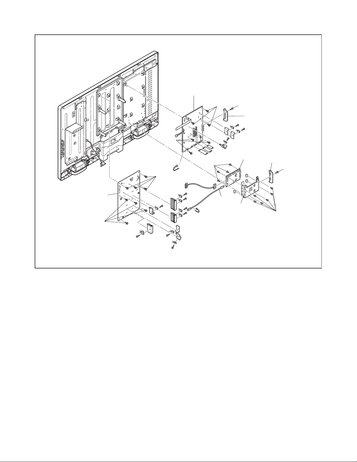
CABINET DISASSEMBLY INSTRUCTIONS
[LD427SSX (Serial No. : DS1A**********),
42MD459B/F7 (Serial No. : DS1A**********)]
1. Disassembly Flowchart
This flowchart indicates the disassembly steps for the
cabinet parts, and the CBA in order to gain access to
item(s) to be serviced. When reassembling, follow the
steps in reverse order. Bend, route and dress the
cables as they were.
[1] Stand
Assembly
[24] Junction
CBA
[3] EMI Shield
[4] BD Loader
Shield
[5] SD CBA
[6] BD Main CBA
& BD Mechanism
Assembly
[7] BD Loader
Retainer
[8] BD Power
CBA
[9] Motor DC Fan
[2] Rear Cabinet
[11] Jack Holder
(D)
[12] Digital Main
CBA Unit
[13] Jack Holder
(A)
[14] Jack Power
CBA
[17] PCB Holder
[19] AC Inlet
Holder
[20] Speaker
Box(es) [B]
[25] Function
CBA
[15] Inverter
Power CBA
[16] Wall Mount
Bracket
2. Disassembly Method
Removal
Step/
Loc.
No.
[1]
[2]
Part
Stand
Assembly
Rear
Cabinet
Fig.
[3] EMI Shield D2 4(S-6) ---
BD Loader
[4]
Shield
[5] SD CBA
BD Main
CBA & BD
[6]
Mechanism
Assembly
BD Loader
[7]
Retainer
BD Power
[8]
CBA
Motor DC
[9]
Fan
BD Loader
[10]
Holder
Remove/*Unhook/
Unlock/Release/
No.
Unplug/Unclamp/
Desolder
D1 4(S-1), 4(S-2) ---
D1 11(S-3), 2(S-4), (S-5) ---
4(S-7), 6(S-8),
D2
*CN2401, *CN2402,
D6
HDMI Cable
D2D62(S-9), *CN2801, SD
Card
2(S-10), (S-11),
D2
4(S-12), 4(S-13),
D6
*CN501, *CN6001,
*CN7101
D2 --------------- ---
D2
5(S-14), *CN2501 ---
D6
D2 2(S-15) ---
D2 --------------- ---
Note
---
---
1
[10] BD Loader
Holder
[18] BD Loader
Bracket
[21] Speaker(s)
[26] IR Sensor
CBA
[22] Stand
Bracket
[23] LCD Module
Assembly
[27] Front
Cabinet
Jack
[11]
Holder(D)
D3 (S-16) ---
6(S-17), 4(S-18),
Digital Main
[12]
CBA UnitD3D6
*CN201, *CN202,
*CN903, *CN3901,
HDMI Cable, Shield
---
Box
Jack
[13]
Holder(A)
Jack Power
[14]
CBA
Inverter
[15]
Power CBAD3D6
Wall Mount
[16]
Bracket
D3 (S-19) ---
6(S-20), *CN203,
D3
*CN801, *CN802,
D6
*CN902, *CN1501
8(S-21), *CN1601,
*CN1803, *CN1804
---
---
D4 4(S-22) ---
5-1 FL9.5-1DC
Page 16

Removal
Step/
Loc.
No.
[17] PCB Holder D4 4(S-23) ---
[18]
[19]
[20]
[21] Speaker(s) D4 Speaker Box(es) [F] ---
Part
BD Loader
Bracket
AC Inlet
Holder
Speaker
Box(es) [B]
Remove/*Unhook/
Fig.
No.
D4 6(S-24), 2(S-25) ---
D4 2(S-26) ---
D4 4(S-27), 10(S-28) ---
Unlock/Release/
Unplug/Unclamp/
Desolder
Note
Stand
[22]
Bracket
LCD
[23]
Module
Assembly
Junction
[24]
CBA
Function
[25]
CBA
IR Sensor
[26]
CBA
Front
[27]
Cabinet
↓
(1)
Note:
(1) Order of steps in procedure. When reassembling,
follow the steps in reverse order. These numbers
are also used as the Identification (location) No. of
parts in figures.
(2) Parts to be removed or installed.
(3) Fig. No. showing procedure of part location
(4) Identification of parts to be removed, unhooked,
unlocked, released, unplugged, unclamped, or
desoldered.
P = Spring, L = Locking Tab, S = Screw,
H = Hex Screw, CN = Connector
* = Unhook, Unlock, Release, Unplug, or Desolder
e.g. 2(S-2) = two Screws (S-2),
2(L-2) = two Locking Tabs (L-2)
(5) Refer to the following "Reference Notes in the
Ta bl e ."
↓
(2)
2(S-29), 2(S-30),
D4
4(S-31), 2(S-32)
D5 6(S-33) ---
D5
Desolder ---
D6
D5
*WH1301B ---
D6
D5
--------------- ---
D6
D5 --------------- ---
↓
(3)
↓
(4)
---
(5)
↓
Reference Notes
1. The BD Main CBA & BD Mechanism Assembly
is adjusted as a unit at factory. Therefore, do
not disassemble it. Replace the BD Main CBA
& BD Mechanism Assembly as a unit.
5-2 FL9.5-1DC
Page 17

(S-3)
[2] Rear Cabinet
(S-3)
[1] Stand Assembly
(S-1)
(S-2)
(S-3)
(S-5)
(S-4)
(S-3)
Fig. D1
5-3 FL9.5-1DC
Page 18

(S-8)
[4] BD Loader Shield
[5] SD CBA
(S-9)
(S-8)
SD Card
(S-12)
[6] BD Main CBA &
BD Mechanism Assembly
[9] Motor DC Fan
[7] BD Loader Retainer
(S-10)
(S-13)
(S-6)
[3] EMI Shield
HDMI Cable
(S-14)
(S-15)
[10] BD Loader Holder
(S-14)
[8] BD
Power CBA
(S-11)
(S-7)
Fig. D2
5-4 FL9.5-1DC
Page 19

[14] Jack Power CBA
[15] Inverter
Power CBA
(S-21)
(S-20)
(S-21)
(S-18)
HDMI Cable
(S-20)
(S-19)
[13] Jack Holder(A)
[12] Digital Main
CBA Unit
Shield Box
[11] Jack Holder(D)
(S-16)
(S-17)
Fig. D3
5-5 FL9.5-1DC
Page 20

[20] Speaker
Box [B]
[21] Speaker
(S-29)
(S-28)
[17] PCB Holder
Speaker
Box [F]
(S-27)
(S-23)
[21] Speaker
(S-29)
(S-28)
(S-32)
[20] Speaker
Box [B]
Speaker
Box [F]
(S-27)
(S-31)
(S-30)
(S-30)
(S-32)
(S-25)
(S-31)
[19] AC Inlet
Holder
(S-26)
(S-25)
[22] Stand
Bracket
(S-22)
[18] BD Loader
Bracket
[16] Wall Mount Bracket
(S-24)
Fig. D4
5-6 FL9.5-1DC
Page 21

[27] Front Cabinet
[25] Function CBA
[26] IR Sensor
CBA
[24] Junction
(S-33)
CBA
[23] LCD Module
Assembly
(S-33)
Fig. D5
5-7 FL9.5-1DC
Page 22

3. TV Cable Wiring Diagram
Function
CBA
Inverter Power CBA
CN1901
CN1902
CN1601
CN1803
CN1804
To LCD Module
Assembly
CN1802
CN1501
*1 This part is directly soldered
on CBA.
Jack Power CBA
CN902
*1
CN601
CN801
CN802
CN203 CN202 CN201
CN903
CN2402
CN2102
*1
WH1301B
CN2401
CN2501
CN2103
CN2101
To AC Inlet
IR Sensor CBA
*1 *1 *1
WH1301A
WH1302B
BD Power CBA
To Fa n
CN7101
To Speaker
Junction
CBA
CN1302WH1302A
SD Card Slot
CN6001
CN501
SD CBA
CN2803
CN7601
JK7501
CN3702
CN3901
JK3804
CN4001
CN3701
Digital Main CBA Unit
To LCD Module
Assembly
CN2801
HDMI Cable
BD Main CBA
5-8 FL9.5-1DC
Fig. D6
Page 23

4. How to Eject Manually
Note: When rotating the gear, be careful not to damage the gear.
1. Remove the BD Main CBA & BD Mechanism Assembly, as shown in Fig. D2.
2. Remove the 4 connectors (CN101, CN601, CN602, CN603) & the 11 screws.
3. Remove the BD Main CBA & Loader cover.
4. Rotate the gear in the direction of the arrow as shown below.
5. Remove a disc.
View for A
BD Main CBA
Loader Cover
A
Rotate this gear in
the direction of the arrow
5-9 FL9.5-1DC
Page 24

CABINET DISASSEMBLY INSTRUCTIONS
[LD427SSX (Serial No. : YA2A**********),
42MD459B/F7 (Serial No. : YA2A**********)]
1. Disassembly Flowchart
This flowchart indicates the disassembly steps for the
cabinet parts, and the CBA in order to gain access to
item(s) to be serviced. When reassembling, follow the
steps in reverse order. Bend, route and dress the
cables as they were.
[1] Stand Base
Assembly
[3] Stand Sub
Cover
[27] Function
CBA
[17] Inverter
Power CBA
[18] Wall Mount
Bracket
[26] Junction
CBA
[5] EMI Shield
[6] BD Loader
Shield
[7] SD CBA
[8] BD Main CBA
& BD Mechanism
Assembly
[9] BD Loader
Retainer
[10] BD Power
CBA
[11] Motor DC
Fan
[12] BD Loader
Holder
[20] BD Loader
Bracket
[2] Stand Hinge
[4] Rear Cabinet
Assembly
[13] Jack Holder
(D)
[14] Digital Main
CBA Unit
[15] Jack Holder
(A)
[16] Jack Power
CBA
[19] PCB Holder
[21] AC Inlet
Holder
[22] Speaker
Box(es) [B]
[23] Speaker(s)
[28] IR Sensor
CBA
[24] Stand
Bracket
[25] LCD Module
Assembly
[29] Front Cabinet
Assembly
2. Disassembly Method
Removal
Step/
Loc.
No.
[1]
[2]
[3]
Part
Stand Base
Assembly
Stand
Hinge
Stand Sub
Cover
Fig.
Rear
[4]
Cabinet
Assembly
[5] EMI Shield D2 4(S-6) ---
BD Loader
[6]
Shield
[7] SD CBA
BD Main
CBA & BD
[8]
Mechanism
Assembly
BD Loader
[9]
Retainer
BD Power
[10]
CBA
Motor DC
[11]
Fan
BD Loader
[12]
Holder
Jack
[13]
Holder(D)
Digital Main
[14]
CBA UnitD3D6
Jack
[15]
Holder(A)
Remove/*Unhook/
Unlock/Release/
No.
Unplug/Unclamp/
Desolder
D1 4(S-1) ---
D1 4(S-2a) ---
D1 2(S-2b) ---
D1 11(S-3), 2(S-4), (S-5) ---
4(S-7), 6(S-8),
D2
*CN2401, *CN2402,
D6
HDMI Cable
D2D62(S-9), *CN2801, SD
Card
2(S-10), (S-11),
D2
4(S-12), 4(S-13),
D6
*CN501, *CN6001,
*CN7101
D2 --------------- ---
D2
5(S-14), *CN2501 ---
D6
D2 2(S-15) ---
D2 --------------- ---
D3 (S-16) ---
6(S-17), 4(S-18),
*CN201, *CN202,
*CN903, *CN3901,
HDMI Cable, Shield
Box
D3 (S-19) ---
Note
---
---
1
---
5-10 FL9.5-2DC
Page 25

Removal
Step/
Loc.
No.
[16]
[17]
[18]
[19] PCB Holder D4 4(S-23) ---
[20]
[21]
[22]
[23] Speaker(s) D4 Speaker Box(es) [F] ---
Part
Jack Power
CBA
Inverter
Power CBAD3D6
Wall Mount
Bracket
BD Loader
Bracket
AC Inlet
Holder
Speaker
Box(es) [B]
Remove/*Unhook/
Fig.
No.
D3
D6
D4 4(S-22) ---
D4 6(S-24), 2(S-25) ---
D4 2(S-26) ---
D4 4(S-27), 10(S-28) ---
Unlock/Release/
Unplug/Unclamp/
Desolder
6(S-20), *CN203,
*CN801, *CN802,
*CN902, *CN1501
8(S-21), *CN1601,
*CN1803, *CN1804
Note
---
---
e.g. 2(S-2) = two Screws (S-2),
2(L-2) = two Locking Tabs (L-2)
(5) Refer to the following "Reference Notes in the
Ta bl e ."
Reference Notes
1. The BD Main CBA & BD Mechanism Assembly
is adjusted as a unit at factory. Therefore, do
not disassemble it. Replace the BD Main CBA
& BD Mechanism Assembly as a unit.
Stand
[24]
Bracket
LCD
[25]
Module
Assembly
Junction
[26]
CBA
Function
[27]
CBA
IR Sensor
[28]
CBA
Front
[29]
Cabinet
Assembly
↓
(1)
Note:
(1) Order of steps in procedure. When reassembling,
follow the steps in reverse order. These numbers
are also used as the Identification (location) No. of
parts in figures.
(2) Parts to be removed or installed.
(3) Fig. No. showing procedure of part location
(4) Identification of parts to be removed, unhooked,
unlocked, released, unplugged, unclamped, or
desoldered.
P = Spring, L = Locking Tab, S = Screw,
H = Hex Screw, CN = Connector
* = Unhook, Unlock, Release, Unplug, or Desolder
↓
(2)
2(S-29), 2(S-30),
D4
4(S-31), 2(S-32)
D5 6(S-33) ---
D5
Desolder ---
D6
D5
*WH1301B ---
D6
D5
--------------- ---
D6
D5 --------------- ---
↓
(3)
↓
(4)
---
(5)
↓
5-11 FL9.5-2DC
Page 26

(S-3)
[4] Rear Cabinet
Assembly
(S-3)
[1] Stand Base
Assembly
(S-1)
(S-5)
(S-4)
(S-3)
(S-2a)
[2] Stand Hinge
[3] Stand Sub Cover
(S-2b)
(S-3)
Fig. D1
5-12 FL9.5-2DC
Page 27

(S-8)
[6] BD Loader Shield
[7] SD CBA
(S-9)
(S-8)
SD Card
(S-12)
[8] BD Main CBA &
BD Mechanism Assembly
[11] Motor DC Fan
[9] BD Loader Retainer
(S-10)
(S-13)
(S-6)
[5] EMI Shield
HDMI Cable
(S-14)
(S-15)
[12] BD Loader Holder
(S-14)
[10] BD
Power CBA
(S-11)
(S-7)
Fig. D2
5-13 FL9.5-2DC
Page 28
[16] Jack Power CBA
[17] Inverter
Power CBA
(S-21)
(S-20)
(S-21)
(S-18)
HDMI Cable
(S-20)
(S-19)
[15] Jack Holder(A)
[14] Digital Main
CBA Unit
Shield Box
[13] Jack Holder(D)
(S-16)
(S-17)
Fig. D3
5-14 FL9.5-2DC
Page 29

[22] Speaker
Box [B]
[23] Speaker
(S-29)
(S-28)
[19] PCB Holder
Speaker
Box [F]
(S-27)
(S-23)
[23] Speaker
(S-29)
(S-28)
(S-32)
[22] Speaker
Box [B]
Speaker
Box [F]
(S-27)
(S-31)
(S-30)
(S-30)
(S-32)
(S-25)
(S-31)
[21] AC Inlet
Holder
(S-26)
(S-25)
[24] Stand
Bracket
(S-22)
[20] BD Loader
Bracket
[18] Wall Mount Bracket
(S-24)
Fig. D4
5-15 FL9.5-2DC
Page 30

[29] Front Cabinet Assembly
[27] Function CBA
[28] IR Sensor
CBA
[26] Junction
(S-33)
CBA
[25] LCD Module
Assembly
(S-33)
Fig. D5
5-16 FL9.5-2DC
Page 31

3. TV Cable Wiring Diagram
Function
CBA
Inverter Power CBA
CN1901
CN1902
CN1601
CN1803
CN1804
To LCD Module
Assembly
CN1802
CN1501
*1 This part is directly soldered
on CBA.
Jack Power CBA
CN902
*1
CN601
CN801
CN802
CN203 CN202 CN201
CN903
CN2402
CN2102
*1
WH1301B
CN2401
CN2501
CN2103
CN2101
To AC Inlet
IR Sensor CBA
*1 *1 *1
WH1301A
WH1302B
BD Power CBA
To Fa n
CN7101
To Speaker
Junction
CBA
CN1302WH1302A
SD Card Slot
CN6001
CN501
SD CBA
CN2803
CN7601
JK7501
CN3702
CN3901
JK3804
CN4001
CN3701
Digital Main CBA Unit
To LCD Module
Assembly
CN2801
HDMI Cable
BD Main CBA
5-17 FL9.5-2DC
Fig. D6
Page 32

4. How to Eject Manually
Note: When rotating the gear, be careful not to damage the gear.
1. Remove the BD Main CBA & BD Mechanism Assembly, as shown in Fig. D2.
2. Remove the 4 connectors (CN101, CN601, CN602, CN603) & the 11 screws.
3. Remove the BD Main CBA & Loader cover.
4. Rotate the gear in the direction of the arrow as shown below.
5. Remove a disc.
View for A
BD Main CBA
Loader Cover
A
Rotate this gear in
the direction of the arrow
5-18 FL9.5-2DC
Page 33

ELECTRICAL ADJUSTMENT INSTRUCTIONS
General Note: “CBA” is abbreviation for
“Circuit Board Assembly.”
Note: Electrical adjustments are required after
replacing circuit components and certain
mechanical parts. It is important to perform
these adjustments only after all repairs and
replacements have been completed.
Also, do not attempt these adjustments unless
the proper equipment is available.
Test Equipment Required
1. NTSC Pattern Generator (Color Bar W/White
Window, Red Color, Dot Pattern, Gray Scale,
Monoscope, Multi-Burst)
2. Remote control unit
3. Color Analyzer
How to make the Service remote
control unit:
Cut “A” portion of the attached remote control unit as
shown in Fig. 1.
How to set up the service mode:
Service mode:
1. Use the service remote control unit.
2. Turn the power on.
3. Press the service button on the service remote
control unit. The following screen appears.
"*" differs depending on the models.
Code :
***********-***
Pic code :
**-***-**-*****-***
MIPS :
Push 0key
Press "Power" key to exit.
Tuner :
****-*****-****
safety_Non
Safety :
service button
A
Fig. 1
6-1 FL9.5EA
Page 34

1. Purity Check Mode
2. VCOM Adjustment
This mode cycles through full-screen displays of red,
green, blue, and white to check for non-active pixels.
1. Enter the Service mode.
2. Each time pressing [7] button on the service
remote control unit, the display changes as
follows.
Purity Check Mode
White mode
[7] button
[7] button
Black mode
[7] button
Red mode
[7] button
Green mode
[7] button
Blue mode
Test Point Adj. Point
Screen
[CHANNEL UP/DOWN ]
buttons
M. EQ. Spec.
Color analyzer See below
Figure
To avoid interference from ambinent
light, this adjustment should be
performed in a dark room.
Perpendicularity
L = 3 cm
Color Analyzer
1. Operate the unit for more than 20 minutes.
2. Set the color analyzer and bring the optical
receptor to the center on the LCD-Panel surface
after zero point calibration as shown above.
Note: The optical receptor must be set
perpendicularly to the LCD Panel surface.
3. Enter the Service mode.
4. Press [3] button on the service remote control unit.
5. Press [CHANNEL UP/DOWN] buttons on the
service remote control unit so that the color
analyzer value becomes minimum.
[7] button
White 20% mode
Note:
When entering this mode, the default setting is White mode.
6-2 LC7NEA
Page 35

The white balance adjustment should be
performed when replacing the LCD Panel
or Digital CBA.
3. White Balance Adjustment
Purpose: To mix red, green and blue beams correctly
for pure white.
Symptom of Misadjustment: White becomes bluish
or reddish.
Test Point
Screen
Adj. Point Mode Input
[VOLUME
DOWN]
button
[VIDEO1]
C/D
M. EQ. Spec.
White Raster
(APL 70%)
or
(APL 40%)
5. [CUTOFF]
Press [1] button to select “COR” for Red Cutoff
adjustment. Press [3] button to select “COB” for
Blue Cutoff adjustment.
[DRIVE]
Press [4] button to select “DR” for Red Drive
adjustment. Press [6] button to select “DB” for Blue
Drive adjustment.
6. In each color mode, press [CHANNEL UP/DOWN]
buttons to adjust the values of color.
7. Adjust Cutoff and Drive so that the color
temperature becomes 12000°K (x
=
0.272 / y
=
0.278 ±0.005).
Pattern Generator,
Color analyzer
x= 0.272 ± 0.005
y= 0.278 ± 0.005
Figure
To avoid interference from ambinent
light, this adjustment should be
performed in a dark room.
Perpendicularity
L = 3 cm
INPUT: WHITE 70%, 40%
Color Analyzer
1. Operate the unit for more than 20 minutes.
2. Input the White Raster(70%=70IRE, 40%=40IRE).
INPUT SIGNAL
0IRE 0IRE
Low
Hight
Light
Light
100IRE
40%=40IRE
70%=70IRE
100IRE
3. Set the color analyzer to the CHROMA mode and
bring the optical receptor to the center on the
LCD-Panel surface after zero point calibration as
shown above.
Note: The optical receptor must be set
perpendicularly to the LCD Panel surface.
4. Enter the Service mode. Press [VOLUME DOWN]
button on the service remote control unit and select
“C/D” mode.
6-3 LC7NEA
Page 36

HOW TO INITIALIZE THE LCD TV/BD
The purpose of initialization is to place the set in a new out of box condition. The customer will be prompted to
select a language and program channels after the set has been initialized.
To put the program back at the factory-default, initialize the LCD TV/BD using the following procedure.
< BD Section >
1. Turn the power on.
2. To enter the service mode, press the service
button on the service remote control unit.
- To cancel the service mode, press [POWER]
button on the service remote control unit.
3. To put the LCD TV/BD into the BD mode, press
[CH RETURN] or [PREV CH] on the service
remote control unit.
4. To put the LCD TV/BD into the Flash clear mode,
press [INPUT SELECT] or [SOURCE] buttons on
the service remote control unit in that order within
five seconds.
The following screen appears.
"*******" differs depending on the models.
7. SD CARD TEST
Write Protect : OK
SD Card Format : OK
SD Capacity : ***
Model Name ******* Region A-1
Release Ver. *.***
When “SD Card Format : OK” appears on the
screen, press [BACK] button on the service
remote control unit.
5. If screen returns to "BD Test Mode", press [8]
button.
"*******" differs depending on the models.
TEST MODE
1: MECHA TEST
2: VFD/LED TEST
3: ERROR RATE MEASURE
4: LD TEST
5: CHANNEL TEST
6: ETC TEST
7: SD CARD TEST
8: DEFAULT SETTING
When “Default Setting : OK” appears on the
screen, the factory default will be set.
"*******" differs depending on the models.
8: DEFAULT SETTING
Default Setting : OK
Model Name ******* Region A-1
Release Ver. *.***
6. To exit this mode, press panel [POWER] button to
turn the power off.
Note: The name of buttons may vary with the brand
of unit.
< LCD TV Section >
1. Turn the power on.
2. To enter the service mode, press the service
button on the service remote control unit.
- To cancel the service mode, press [POWER]
button on the service remote control unit.
3. Press [INFO] button on the service remote control
unit to initialize the LCD television.
4. "INITIALIZED" will appear in the upper right of the
screen. "INITIALIZED" color will change to green
from red when initializing is complete.
Model Name ******* Region A-1
Release Ver. *.***
7-1 FL9.5INT
Page 37

FIRMWARE RENEWAL MODE
)
< BD Section >
1. Turn the power on and press [EJECT] button on
the remote control unit to put the LCD TV/BD into
BD mode. Then remove the disc.
2.
To put the LCD TV/BD into F/W version up mode,
press [9], [8], [7], [6], and [POP MENU] or [MENU/
EXIT] buttons on the remote control unit in that order.
Fig. a appears on the screen.
"
" differs depending on the models.
*******
F/W VERSION UP MODE F/W Name: ******* Ver. *.***
Now Loading...
(*1)
http://*******
Fig. a
•
URL as shown below is displayed in (*1) of Fig. a.
(URL is different depending on the models.)
[LD427SSX]:
http://sylvaniaconsumerelectronics.com
[42MD459B/F7]: http://www.magnavox.com
• The current F/W version of the BD is displayed in (*2).
• The current F/W version of the TV is displayed in (*3).
3. Insert the disc for version up into the disc slot.
4. Press [ENTER] or [OK] button to select “1. ALL”.
(Fig. b)
"
" differs depending on the models.
*******
F/W VERSION UP MODE F/W Name: ******* Ver. *.***
Please Select F/W Update Mode
1. ALL
2. FE
3. BE
http://*******
EXIT : POWER
Fig. b
5. The LCD TV/BD enters the F/W version up mode
automatically. Fig. c appears on the screen. Make sure
to insert the proper F/W for the state of this model.
"
" differs depending on the models.
*******
F/W VERSION UP MODE F/W Name: ******* Ver. *.***
1. ALL
Version: *.*** ***********XA1.b20
(*4)
Reading...
******_*.*
******_*.*
(*2)
(*3
The appearance shown in (*4) of Fig. c is
described as follows:
No. Appearance State
1 Reading... Sending files into the memory
2
See FL
Display
Erasing previous version data
and writing new version data.
6. After programming is finished, the disc will be
ejected automatically.
At this time, no button is available.
7. Remove the disc.
8. Unplug the AC cord from the AC outlet. Then plug
it again.
9. Press [EJECT] button on the remote control unit to
put the LCD TV/BD into BD mode again.
10. Press [1], [2], [3], [4], and [INFO] buttons on the
remote control unit in that order.
Fig. d appears on the screen.
"
" differs depending on the models.
Version Info
F/W Name : *******
Version : *.***
Region : A-1
*******
EXIT : POWEREEPROM CLEAR <STOP>
Fig. d
11. Press [STOP] button on the remote control unit.
Fig. e appears on the screen.
"
" differs depending on the models.
Version Info
F/W Name : *******
Version : *.***
Region : A-1
EEPROM CLEAR : OK
*******
EXIT : POWEREEPROM CLEAR <STOP>
Fig. e
When “OK” appears on the screen, the factory
default will be set. Then the firmware renewal
mode is complete.
12. Press [POWER] button to turn the power off.
Note: The name of buttons may vary with the brand
of unit.
http://*******
Fig. c
EXIT : POWER
******_*.*
8-1 FL9.5FW
Page 38

< LCD TV Section >
Equipment Required
a. USB memory
b. Remote Control Unit
Firmware Update Procedure
Note: There are two states (the User Upgrade and
the Factory Upgrade) in firmware update.
User Upgrade Upgrade the firmware only.
The setting values are not
initialized.
Factory upgrade Upgrade the firmware and
initialize the setting values.
The identification of User Upgrade and Factory
Upgrade are done by the filename.
1. Turn the power off and unplug the AC Cord.
2. Insert the USB memory to the USB port as shown
below.
Note: If the above screen isn’t displayed, repeat from
step 1.
The appearance shown in *1 is described as follows.
Appearance State
Downloading...
Writing...
Downloading the firmware from
the USB memory.
Writing the downloaded firmware
in flash memory.
Checking... Checking the new firmware.
5. When the firmware update is completed, the
following will appear on the screen.
Software Upgrade
The software upgrade is completed.
Remove USB storage device, unplug and replug power code.
USB port
USB Memory
Rear Cabinet
3. Plug the AC cord in the wall outlet and turn the
power on.
4. The update will start and the following will appear
on the screen.
Software Upgrade
Unplug the AC cord and kindly remove the USB
memory from the USB port. Plug the AC cord in
the wall outlet again and turn the power on.
Note:
When the Factory Upgrade is used, after
restarting TV, shift to initial screen menu in service
mode. "INITIALIZED" will appear on the upper
right of the screen. "INITIALIZED" color will
change to green from red when initializing is
complete.
*1
Software upgrade in progress. Please wait.
Do not remove the USB device or turn the TV off
while upgrade is in progress.
Downloading...
0%
8-2 FL9.5FW
Page 39

TROUBLESHOOTING
[ Power Supply Section ]
( Inverter Power CBA, BD Power CBA )
FLOW CHART NO.1
The power cannot be turned on.
Is the fuse (F1601) normal?
Ye s
Is normal state restored when once un
power cord is plugged again several seconds?
Ye s
Is the AL+5V line voltage normal?
Ye s
Is the PANEL+24V line voltage normal?
Ye s
Check each rectifying circuit of the secondary
circuit and service it if defective.
FLOW CHART NO.2
The fuse blows out.
Check the presence that the primary component
is leaking or shorted and service it if defective.
plugged
No
No
No
No
See FLOW CHART No.2 <The fuse blows out.>
Check if there is any leak or short-circuiting on the
primary circuit component, and service it if defective.
(D1205, D1206, D1207, D1208, Q1203, Q1204,
T1201)
Check if there is any leak or short-circuiting on the
primary circuit component, and service it if defective.
(D1601, IC1401, IC1702, Q1601, Q1602, Q1701,
Q1702, T1701)
Check the presence that the rectifying diode or circuit
is shorted in each rectifying circuit of secondar
and service it if defective.
y side,
After servicing, replace the fuse.
FLOW CHART NO.3
When the output voltage fluctuates.
Does the photocoupler circuit on the
secondary side operate normally?
Ye s
Check D1210, D1904, IC1202, IC1702, IC1704, IC1901
and their periphery, circuit and service it if defective.
FLOW CHART NO.4
When buzz sound can be heard in the vicinity of power circuit.
Check if there is any short-circuit on the rectifying diode and the circ
and service it if defective. (D1101, D1714, D1715, D1912, D1915, D1919, D1920, D1921, IC2201, IC2301, IC2401,
Q1101, Q1904, Q2402, Q2403, Q2405)
No
Check D1213, D1720, D1917, IC1202, IC1704,
IC1901 and their periphery circuit, and service it
if defective.
uit in each rectifying circuit of the secondary side,
9-1 FL9.5TR
Page 40

FLOW CHART NO.5
AL+5V is not output.
Is approximately +5V voltage supplied to the
cathode of D1101?
Ye s
Check if there is any leak or short-circuit on the loaded
circuit, and service it if defective.
FLOW CHART NO.6
AL+3.3V is not output.
Is approximately +5V voltage supplied to the collector
of Q1101?
Ye s
Is approximately +4V voltage supplied to the base
of Q1101?
Ye s
Replace Q1101.
FLOW CHART NO.7
+12V is not output.
Is approximately +12V voltage supplied to the cathod
of D1912?
Ye s
No
No
No
No
Check C1103, D1101, D1102 and their periphery
circuit, and service it if defective.
Check C1103, D1101, D1102 and their periphery
circuit, and service it if defective.
Check D1109 and their periphery circuit, and
service it if defective.
Check C1923, D1912, D1916 and their periphery
circuit, and service it if defective.
Check if there is any leak or short-circuit on the loaded
circuit, and service it if defective.
FLOW CHART NO.8
+10.5V is not output.
Is approximately +12V voltage supplied to the emitter
of Q1904?
Ye s
Is the "H" pulse inputted to the base of Q
Ye s
Check Q1904, Q1905 and their per
service it if defective.
FLOW CHART NO.9
P-ON+3.3V is not output.
Is approximately +5V voltage supplied to Pin(1) of
IC2401?
Ye s
Replace IC2401.
1905?
iphery circuit, and
No
No
No
Check C1923, D1912, D1916 and their periphery
circuit, and service it if defective.
Check DVD-P-ON1 line and their periphery circuit,
and service it if defective.
Check Q2401, Q2405, DVD-P-ON1 line and their
periphery circuit, and service it if defective.
9-2 FL9.5TR
Page 41

FLOW CHART NO.10
P-ON+1.2V is not output.
Is approximately +12V voltage supplied to Pin(3) of
IC2201?
Ye s
Is the "H" pulse inputted to Pin(8) of IC2201?
Ye s
Replace IC2201.
FLOW CHART NO.11
P-ON+1.8V is not output.
Is approximately +5V voltage supplied to Pin(3) of
IC2301?
Ye s
Is the "H" pulse inputted to Pin(8) of
Ye s
Replace IC2301.
FLOW CHART NO.12
P-ON+5V(1) is not output.
IC2301?
No
No
No
No
See FLOW CHART NO.7 <+12V is not output.>
Check Q2201, Q2202 and their periphery circuit,
and service it if defective.
Check C1924, D1915, D1919, D1921 and their
periphery circuit, and service it if defective.
Check Q2301, Q2302 and their periphery circuit,
and service it if defective.
Is approximately +5V voltage supplied to the emitter
of Q2402?
Ye s
Check D2402, Q2404, DVD-P-ON2 line and their
periphery circuit, and service it if defective.
FLOW CHART NO.13
P-ON+5V(2) / USB+5V / AUDIO+5V is not output.
Is approximately +5V voltage supplied to the emitter
of Q2403?
Ye s
Check D2403, Q2404, DVD-P-ON2 line and their
periphery circuit, and service it if defective.
No
No
Check C1924, D1915, D1919, D1921 and their
periphery circuit, and service it if defective.
Check C1924, D1915, D1919, D1921 and their
periphery circuit, and service it if defective.
9-3 FL9.5TR
Page 42

( Jack Power CBA )
FLOW CHART NO.14
When the output voltage fluctuates.
Does the photocoupler circuit on the
secondary side operate normally?
Ye s
Check D607, IC601 and their periphery, circuit and
service it if defective.
FLOW CHART NO.15
When buzz sound can be heard in the vicinity of power circuit.
Check if there is any short-circuit on the rectifying diode and the circuit in each re
and service it if defective. (D613, D615, D617, D618, D620, D621, D622, D623, D624, IC602, Q603, Q604, Q605)
FLOW CHART NO.16
TUNER+31V is not output.
Is approximately +40V voltage supplied to the
cathode of D618?
Ye s
Check D632, R640 and their periphery circuit, and
service it if defective.
No
No
Check D616, D637, IC601 and their periphery
circuit, and service it if defective.
ctifying circuit of the secondary side,
Check C617, D618, D619 and their periphery
circuit, and service it if defective.
FLOW CHART NO.17
P-ON+8.2V is not output.
Is approximately +16.5V voltage supplied to the
collector of Q603?
Ye s
Is approximately +9V voltage supplied to the
base of Q603?
Ye s
Replace Q603.
No
No
Check C622, C624, D617, D624 and their periphery
circuit, and service it if defective.
Check D627, D628 and their periphery circuit, and
service it if defective.
9-4 FL9.5TR
Page 43

FLOW CHART NO.18
P-ON+5V is not output.
Is approximately +6V voltage supplied to the
collector of Q604?
Ye s
Is approximately +6V voltage supplied to the
base of Q604?
Ye s
Replace Q604.
FLOW CHART NO.19
P-ON+3.3V is not output.
Is approximately +5V voltage supplied to the
collector of Q605?
Ye s
Is approximately +4V voltage supplied to the
base of Q605?
Ye s
Replace Q605.
No
No
No
No
Check C619, D620 and their periphery circuit,
and service it if defective.
Check D638 and their periphery circuit, and service
it if defective.
Check C621, D623 and their periphery circuit, and
service it if defective.
Check D631 and their periphery circuit, and service
it if defective.
9-5 FL9.5TR
Page 44

[ Video Signal Section ]
FLOW CHART NO.1
The key operation is not functioning.
Are the contact point and installation state of the key
switches (SW1351~SW1355, SW1357~SW1360)
normal?
Ye s
When pressing each switches (SW1351~SW1355,
SW1357~SW1360) do the voltage of Pin(3) of CN202
and Pin(2) of CN903 increase?
Ye s
Replace Digital Main CBA Unit.
FLOW CHART NO.2
No operation is possible from the remote control unit.
Operation is possible from the remote control unit.
Is 3.3V voltage supplied to Pin(2) terminal of the
remote control receiver (RS1301)?
Ye s
Is the "L" pulse sent out Pin(1) terminal of remote
control receiver (RS1301) when the infrared remote
control is activated?
Ye s
Is the "L" pulse supplied to Pin(1) of CN202?
Ye s
Replace Digital Main CBA Unit.
No
No
No
No
No
Re-install the switches (SW1351~SW1355, SW1357~
SW1360) correctly or replace the poor switch.
Check the switches (SW1351~SW1355, SW1357~
SW1360) and their periphery, and service it if
defective.
Check AL+3.3V line and service it if defective.
Replace the remote control receiver(RS1301)
or the remote control unit.
Check the line between Pin(1) terminal of remote
control receiver(RS1301) and Pin(1) of CN202,
and service it if defective.
9-6 FL9.5TR
Page 45

FLOW CHART NO.3
Picture does not appear normally. (EXT. input)
Are the video signals inputted to each pin of IC401? Check the line between video input terminal and
IC401 VIDEO-IN 13PIN
IC401 Y-IN 11PIN
IC401 C-IN 19PIN
IC401 VIDEO-IN 27PIN
IC401 Y-IN 2 5PIN
IC401 C-IN 2 11PIN
IC401 COMPONENT-Y-IN43PIN
IC401 COMPONENT-Pb-IN47PIN
IC401 COMPONENT-Pr-IN
Ye s
Are the video signals outputted to each pin of IC401?
IC401 CVBS/Y/S-Y-IN38PIN
IC401 Pb-IN36PIN
IC401 Pr/S-C-IN34PIN
Ye s
Replace Digital Main CBA Unit or LCD Module
Assembly.
No
each pin of IC401.
IC401 3PIN
IC401 1PIN
IC401 9PIN
IC401 7PIN
IC401 5PIN
IC401 11PIN
IC401 43PIN
IC401 47PIN
IC401 52PIN
No
Is 5V voltage supplied to the Pin(2, 29, 33, 39, 44) of IC401?
Is 8.2V voltage supplied to the Pin(12) of IC401?
Replace IC401.
→ JK703
→ JK702
→ JK702
→ JK707
→ JK706
→ JK706
→ JK717
→ JK718
→ JK719
Ye s
Check P-ON+5V, P-ON+8.2V line
and service it if defective.
VIDEO-IN 1
Y-IN 1
C-IN 1
VIDEO-IN 2
Y-IN 2
C-IN 2
COMPONENT-Y-IN
COMPONENT-Pb-IN
COMPONENT-Pr-IN52PIN
No
FLOW CHART NO.4
Picture does not appear normally. (Tuner input)
Are the DIF signal inputted to Pin(3, 4)
Ye s
Replace Digital Main CBA Unit or LCD Module
Assembly.
FLOW CHART NO.5
Picture does not appear normally. (BD PB)
Are the HDMI cable(CL3804) connected proper
Ye s
Replace the BD Main CBA & BD Mechanism
Assembly or HDMI cable(CL3804).
of CN201?
ly?
No
No
Check the line between Pin(3, 4) of CN201 and
Pin(12, 13) of TU101, and service it if defective.
Reconnected the HDMI cable(CL3804).
9-7 FL9.5TR
Page 46

[ Audio Signal Section ]
FLOW CHART NO.1
Audio does not appear normally. (EXT. input)
Are the audio(L/R) signals inputted to each pin of
IC401?
IC401 AUDIO(L/R)-IN 1
IC401 16,17PIN
IC401 20,21PIN
IC401 24,25PIN
Are the audio(L/R) signals outputted to Pin(27, 28) of
IC401?
14,15PIN
AUDIO(L/R)-IN 2
COMPONENT AUDIO(L/R)-IN
HDMI AUDIO(L/R)-IN
Ye s
Yes
(Output to audio
output terminal)
Are the audio(L/R) signals outputted to Pin(8, 10) of
CN202?
Ye s
Are the audio(L/R) signals inputted to Pin(1, 44)
of IC801?
Ye s
Are the audio(L/R) signals outputted to CN801 and
CN802?
Ye s
Ye s
(Output to speakers)
No
No
No
Check the line between audio input terminal and
each pin of IC401.
IC401
14,15PIN
IC401
16,17PIN
IC401
20,21PIN
IC401
24,25PIN
Is 5V voltage supplied to the Pin(2, 29, 33, 39, 44) of IC401?
Is 8.2V voltage supplied to the Pin(12) of IC401?
Replace IC401.
Replace Digital Main CBA Unit.
Check the line between Pin(8, 10) of CN202 and
No
Pin(1, 44) of IC801, and service it if defective.
No
Check IC801 and their periphery circuit, and
service it if defective.
→ JK704, JK705
→ JK708, JK709
→ JK712, JK713
→ JK720, JK721
Ye s
Check P-ON+5V, P-ON+8.2V line
and service it if defective.
AUDIO(L/R)-IN 1
AUDIO(L/R)-IN 2
COMPONENT AUDIO(L/R)-IN
HDMI AUDIO(L/R)-IN
No
Check SP801,SP802 and their periphery circuit,
and service it if defective.
Are the audio(L/R) signals outputted to Pin(4, 6) of
CN202?
Ye s
Are the audio(L/R) signals inputted to Pin(3, 5)
of IC803?
Ye s
Are the audio(L/R) signals outputted to Pin(1, 7)
of IC803?
Ye s
Check the line between Pin(1, 7) of IC803 and audio
output terminal(JK722, JK723) and service it if defective.
No
No
No
Replace Digital Main CBA Unit.
Check the line between Pin(4, 6) of CN202 and
Pin(3, 5) of IC803, and service it if defective.
Replace IC803
9-8 FL9.5TR
Page 47

FLOW CHART NO.2
Audio does not appear normally. (Tuner input)
Are the DIF signal inputted to Pin(3, 4) of CN201?
Yes
(Output to audio
output terminal)
Are the audio(L/R) signals outputted to Pin(8, 10) of
CN202?
Ye s
Are the audio(L/R) signals inputted to Pin(1, 44)
of IC801?
Ye s
Are the audio(L/R) signals outputted to CN801 and
CN802?
Ye s
Check SP801,SP802 and their periphery circuit,
and service it if defective.
Are the audio(L/R) signals outputted to Pin(4, 6) of
CN202?
Ye s
Are the audio(L/R) signals inputted to Pin(3, 5)
of IC803?
Ye s
Are the audio(L/R) signals outputted to Pin(1, 7)
of IC803?
Ye s
Check the line between Pin(1, 7) of IC803 and audio
output terminal(JK722, JK723) and service it if defective.
Ye s
(Output to speakers)
No
No
No
No
No
Check the line between Pin(3, 4) of CN201 and
Pin(12, 13) of TU101, and service it if defective.
Replace Digital Main CBA Unit.
Check the line between Pin(8, 10) of CN202 and
No
Pin(1, 44) of IC801, and service it if defective.
No
Check IC801 and their periphery circuit, and
service it if defective.
Replace Digital Main CBA Unit.
Check the line between Pin(4, 6) of CN202 and
Pin(3, 5) of IC803, and service it if defective.
Replace IC803
9-9 FL9.5TR
Page 48

FLOW CHART NO.3
Audio does not appear normally. (BD PB)
Are the HDMI cable(CL3804) connected properly?
Yes
(Output to audio
output terminal)
Are the audio(L/R) signals outputted to Pin(8, 10) of
CN202?
Ye s
Are the audio(L/R) signals inputted to Pin(1, 44)
of IC801?
Ye s
Are the audio(L/R) signals outputted to CN801 and
CN802?
Ye s
Check SP801,SP802 and their periphery circuit,
and service it if defective.
Are the audio(L/R) signals outputted to Pin(4, 6) of
CN202?
Ye s
Are the audio(L/R) signals inputted to Pin(3, 5)
of IC803?
Ye s
Are the audio(L/R) signals outputted to Pin(1, 7)
of IC803?
Ye s
Check the line between Pin(1, 7) of IC803 and audio
output terminal(JK722, JK723) and service it if defective.
Ye s
(Output to speakers)
No
No
No
No
No
Reconnected the HDMI cable(CL3804).
Replace Digital Main CBA Unit.
Check the line between Pin(8, 10) of CN202 and
No
Pin(1, 44) of IC801, and service it if defective.
No
Check IC801 and their periphery circuit, and
service it if defective.
Replace Digital Main CBA Unit.
Check the line between Pin(4, 6) of CN202 and
Pin(3, 5) of IC803, and service it if defective.
Replace IC803
9-10 FL9.5TR
Page 49

BLOCK DIAGRAMS
System Control Block Diagram
AL+3.3V
DVD
POWER
D1302
D1301
SENSOR
REMOTE
RS1301
WH1302B
WH1302A
JUNCTION
CBA
CN1302
CN203
STANDBY
REMOTE22
P-ON-H155
KEY-IN166
LED144
DVD-LED88
REMOTE27
P-ON-H154
KEY-IN163
LED145
DVD-LED81
D1303
IR SENSOR CBAFUNCTION CBA
WH1301A
KEY-IN133
KEY-IN277
KEY-IN272
KEY-IN144
WH1301B
KEY SWITCH
KEY SWITCH
TO
POWER SUPPLY 2
BLOCK DIAGRAM
TO
POWER SUPPLY 1
BLOCK DIAGRAM
P-ON-H2
P-ON-H1
PROTECT3
BACKLIGHT-SW
CN1802
15
PROTECT3
P-ON-H1321
P-ON-H2420
9
CN902
16
BACKLIGHT-SW
8
BACKLIGHT-ADJ
17
BACKLIGHT-ADJ
7
19
POWER-RESET
5
Q501
TO POWER SUPPLY 3
BLOCK DIAGRAM
PROTECT4
DVD-P-ON2
DVD-P-ON1
POWER-RESET
TO BD DIGITAL
SIGNAL PROCESS 1
BLOCK DIAGRAM
DISC-IN
DISC-OUT
IREDCONTV
DISC-OUT24
IREDCONTV51IREDCONTV77IREDCONTV13 11IREDCONTV77
DISC-IN15
CN2103
INVERTER POWER CBA
TXD1
RXD1
IC6001
(MAIN MICRO CONTROLLER)
V32
U34
CN7101
SUB-RXD77
SUB-TXD88
CN2102
BD MAIN CBA
RESET
RDY
E3
T34
SYS-RESET99
RDY10 10
BD POWER CBA
CN2401
DRIVE
Q202 Q201
DVD-LED33
KEY-IN222
CN4001
E5
DVD-LED
IC3301
(MAIN MICRO CONTROLLER)
PROTECT1
CN202CN3702
LED122
REMOTE11
KEY-IN133
F1
R22
AC5
AD6
LED1
KEY-IN1
KEY-IN2
REMOTE
TU101 (TUNER UNIT)
CN201CN3701
PROTECT1
P-ON-H1
P-ON-H2
BACKLIGHT-SW
BACKLIGHT-ADJ
RESET
77PROTECT3
88
66
10 10
AD5
PROTECT1
AUDIO-MUTE
DVD-SPD-EN
SHD-SPD-EN
V6
U6
AB9
R23
AB13
P-ON-H2
P-ON-H1
23 23
AE5
AB16
PROTECT3
BACKLIGHT-SW
25 25
AB23
BACKLIGHT-ADJ
11 11
CN3702 CN202
W26
RESET
SCL
9
28
SCL
28
AC18
SCL
CN1901
CN1802CN902 CN2402CN1902 CN501
JACK POWER CBA
SDA
8
27
SDA
27
IC3103
RESET
AC19
SDA
AL+3.3V
SCK
AB25
DISC-OUT14 10 DISC-OUT99
CN903CN4001
DISC-OUT88
E4
AB17
DISC-OUT
IREDCONTV
SIN
SOUTCSWP
E11
AB24
AC25
AC24
DVD-P-ON211 13
DVD-P-ON112 12
DISC-IN15 9 DISC-IN10 10
SUB-RXD18 6 SUB-RXD11 11
SUB-TXD19 5 SUB-TXD12 12
DVD-RESET20 4 DVD-RESET13 13
PROTECT422 2
DVD-P-ON166
DISC-IN99
PROTECT416 16
U23
AE6
AB18
DISC-IN
PROTECT4
DVD-P-ON1
CLKOUT
CLKIN
N1
N2
DVD-READY21 3 DVD-READY14 14
DVD-P-ON255
SUB-RXD12 12
SUB-TXD13 13
DVD-RESET14 14
DVD-READY15 15
F3
P22
N22
AB10
AC14
TXD1
RXD1
DVD-P-ON2
DVD-RESET
DVD-READY
AUDIO-MUTE
DVD-SPD-EN
SHD-SPD-EN
TO AUDIO
BLOCK
DIAGRAM
10-1
652
1
3
SI
CS
SO
WP
25MHz
SCK
IC3101 (MEMORY)
X3102
OSC
DIGITAL MAIN CBA UNIT
FL9.5BLS
Page 50

Video Block Diagram
TO DIGITAL
SIGNAL
PROCESS
BLOCK
AUDIO SIGNAL
DIAGRAM
TO DIGITAL
SIGNAL
PROCESS
BLOCK
DIAGRAM
VIDEO SIGNAL
DIGITAL MAIN CBA UNIT
Pb-IN
CVBS/Y/S-Y-IN
CVBS/Y/S-Y-IN18 18
CN202 CN3702
383634
Pr/S-C-IN
Pb-IN20 20
Pr/S-C-IN22 22
WF1WF2WF3
IF-AGC
DIF-OUT1
DIF-OUT2
IF-AGC11
DIF-OUT244
DIF-OUT133
CN201 CN3701
IC401
(INPUT SELECTOR)
JACK POWER CBA
VIDEO
SELECTOR
3
1
5
7
9
11414345475052
JK703
VIDEO-IN1
CY
JK702
S-VIDEO
-IN1
JK707
VIDEO-IN2
CY
JK706
S-VIDEO
-IN2
S-VIDEO-SW1
S-VIDEO-SW2
51
49
WITH TWO COMPONENT INPUT
JK714
JK715
COMPONENT
-Y-IN1
JK716
COMPONENT
-Pb-IN1
COMPONENT
-Pr-IN1
JK717
JK718
COMPONENT
-Y-IN2
JK719
COMPONENT
-Pb-IN2
COMPONENT
-Pr-IN2
12
DIF-OUT1
TU101
(TUNER UNIT)
13
14
IF-AGC
DIF-OUT2
10-2 FL9.5BLV
Page 51

Audio Block Diagram
TO BD
DIGITAL
SIGNAL
PROCESS
2 BLOCK
DIAGRAM
TO
DIGITAL
SIGNAL
PROCESS
BLOCK
DIAGRAM
TO
SYSTEM
CONTROL
BLOCK
DIAGRAM
TO
DIGITAL
SIGNAL
PROCESS
BLOCK
DIAGRAM
TO
SYSTEM
CONTROL
BLOCK
DIAGRAM
AUDIO SIGNAL
SPDIF
CN7101
CN2102
BD MAIN CBA
SPDIF55
BD POWER
CBA
DIGITAL MAIN CBA UNIT
DVD-SPDIF99
CN1901 CN2401
INVERTER
POWER CBA
DVD-SPDIF16 8
CN902 CN1802
WF4
AUDIO(L)
CN3702CN202
AUDIO(L)24 24
AUDIO(R)
AUDIO(R)26 26
AUDIO-MUTE
IC3501
(AUDIO DSP)
IC3503
(AUDIO D/A CONVERTER)
BCLK
LRCLK
35
8
(L-CH)
CN202 CN3702
ACLK
ADATA0
ADATA1
4402
39
DSP
373433
36
567
D/A
CONVERTER
(R-CH)
15
14
44
66
88
AUDIO(L)-OUT
AUDIO(R)-OUT
AMP(L)-OUT
3
8
IC3502
(AUDIO D/A CONVERTER)
1010
AMP(R)-OUT
D/A
(L-CH)
(R-CH)
15
567
CONVERTER
14
1313
SPDIF
CN202 CN3702
IC4002
(BUFFER GATE)
1111
AUDIO-MUTE
SHD-SPDIF
2
4
DVD-SPD-EN
SHD-SPD-EN
1
IC4001
(BUFFER GATE)
2
1
4
DVD-SPDIF10 10
CN903 CN4001
IC401
JACK POWER CBA
JK704
(INPUT SELECTOR)
14
AUDIO(L)-IN1
JK705
16
18
AUDIO(R)-IN1
20
24
JK708
28
AUDIO
AUDIO(L)-IN2
JK709
SELECTOR
151719
AUDIO(R)-IN2
27
21
COMPONENT
AUDIO(L)-IN1
JK710
JK711
25
WITH TWO COMPONENT INPUT
COMPONENT
AUDIO(R)-IN1
COMPONENT
JK712
AUDIO(L)-IN2
COMPONENT
JK713
AUDIO(R)-IN2
JK720
HDMI
AUDIO(L)-IN
JK721
HDMI
IC803
(OP AMP)
AUDIO(R)-IN
5
7
JK722
AUDIO(L)-OUT
3
1
MUTE
Q703
JK723
AUDIO(R)-OUT
DRIVE
Q802,Q804
MUTE
Q704
JK701
DIGITAL
BUFFER
Q702
AUDIO-OUT
(COAXIAL)
1
DRIVE1 PWM1
IC801 (AUDIO POWER AMP)
9,10
13,14
CN801
CL801
1
2
SP(L)-
SP(L)+
SP801
SPEAKER
35,36
L-CH
44
DRIVE2 PWM2
31,32
Q801
20
MUTE CONTROL
1
2
CN802
SP(R)-
SP(R)+
CL802
SP802
SPEAKER
R-CH
10-3
FL9.5BLA
Page 52

Digital Signal Process Block Diagram
/
LCD MODULE
ASSEMBLY
LVDS-D1E(+)21
LVDS-D1E(-)22
LVDS-D0E(+)23
LVDS-D0E(-)24
LVDS-D2E(+)19
LVDS-D2E(-)20
LVDS-D3E(+)13
LVDS-D3E(-)14
LVDS-D0O(+)39
LVDS-D0O(-)40
LVDS-D1O(+)37
LVDS-D1O(-)38
LVDS-D2O(+)35
AUDIO SIGNAL
CN3901
LVDS-CE(+)16
LVDS-CE(-)17
LVDS-CO(+)32
LVDS-CO(-)33
LVDS-D2O(-)36
LVDS-D3O(+)29
LVDS-D3O(-)30
IC3201
DATA(0-15)
(DDR2 SDRAM)
ADDESS(0-12)
VIDEO SIGNAL
IC3301 (DIGITAL SIGNAL PROCESS)
H1,H3,H7,H9
B1,B9,C2,C8,
F1,F9,G2,G8,
M2,M3,M7,M8,
N2,N3,N7,N8,
P2,P3,P7,P8,R2
D1,D3,D7,D9,
AF23
AE23
AD23
AD24
A/D
CONVERTER
DEMODULATOR
V3
/MPEG DECODER
AF2
AE2
DIF-OUT1
DIF-OUT2
IF-AGC
SW
V1
V2
AA3
U2
U1
U3
CVBS/Y/S-Y-IN
Pr/S-C-IN
Pb-IN
AF22
IF-AGC
AF7
AE22
AD21
AD22
AF24
AE24
LVD S
M2
M1
AUDIO(R)
AUDIO(L)
AF18
TX
AD9
BCLK
AE18
AD17
AD12
ACLK
LRCLK
AE17
AD18
AUDIO I/F
AD10
AD11
ADATA0
SHD-SPDIF
AC10
AF17
AD14
ADATA1
AF16
AE16
AE19
AF19
AUDIO
DECODER
D1
DIGITAL
SIGNAL
D2
PROCESS
HDMI
C1
C2
A13-15,A18,
A21-23,B13-15,
B17,B19-23
C15,C17-19,
C23,C24,D14,
D15,D17-19,
D22,D23
VIDEO
DECODER
I/F
A1
A2
B1
B2
DIGITAL MAIN CBA UNIT
IC3801 (HDMI SW)
222124232625201943
DATA0(+)
DATA0(-)
DATA1(+)
79461
DATA1(-)
DATA2(+)
JK3803
TO VIDEO
BLOCK DIAGRAM
CLOCK(+)
DATA2(-)
3
101216
HDMI-IN1
CLOCK(-)
HDMI-DATA
44
14131615181712
DATA0(+)
HDMI-CLOCK
79461
15
DATA0(-)
DATA1(+)
DATA1(-)
DATA2(+)
TO AUDIO
BLOCK DIAGRAM
DATA2(-)
CLOCK(+)
3
HDMI-IN2
JK3801
113940
HDMI-DATA
CLOCK(-)
101216
10-4
686770697271666529
HDMI-CLOCK
DATA0(+)
DATA0(-)
79461
15
56575859606162
HDMI
DATA1(+)
DATA1(-)
DATA2(+)
DATA2(-)
CLOCK(+)
3
101216
HDMI-IN3
JK3802
SW
HDMI-DATA
CLOCK(-)
63
30
HDMI-CLOCK
DATA0(+)
15
4365872
DATA0(-)
DATA1(+)
DATA1(-)
DATA2(+)
HDMI-IN
JK3804
DATA2(-)
3
TO BD
79461
1
CLOCK(+)
CLOCK(-)
101216
AUDIO
VIDEO
BLOCK
33
34
HDMI-DATA
HDMI-CLOCK
15
DIAGRAM
(JK7501)
FL9.5BLD
Page 53

Power Supply 1 Block Diagram
AL+3.3V
NOTE:
The voltage for parts in hot circuit is measured using
hot GND as a common terminal.
+3.3V REG.
Q1101
Q1202
Q1201
LCD MODULE
ASSEMBLY
PANEL+24V
1-5
CN1804
PANEL+24V
1-5
CN1803
PROTECT311BACKLIGHT-ADJ13BACKLIGHT-SW
14
BACKLIGHT-SW
BACKLIGHT-ADJ
TO SYSTEM CONTROL
BLOCK DIAGRAM
P-ON-H1
PROTECT3
P-ON-H2
9
8
10
T1201
4
For continued protection against risk of fire,
replace only with same type 4 A, 125V fuse.
CAUTION ! :
ATTENTION : Utiliser un fusible de rechange de même type de 4A, 125V.
BRIDGE
RECTIFIER
4A/125V
D1205-D1208
7
6
Q1203
INVERTER POWER CBA
1
2
SWITCHING
IC1202
(FEED BACK)
11
L1604
2
14
3 2
SWITCHING
Q1204
8
5
SWITCHING
Q1602
14
14
IC1703
(ISOLATOR)
COLD
Q1705
3 2
Q1404
Q1706
RL1201
CONTROL
L1603
11
2
8
5
SWITCHING
Q1601
11
+354V
1091112131415
T1701
8
7
SWITCHING
Q1701
9
534
8
SWITCHING
Q1702
12
2
5
16
1
14
IC1704
(FEED BACK)
4
13
3 2
3
14
IC1705
(ISOLATOR)
Q1703
14
Q1708
Q1707
3 2
Q1704
SWITCHING
LINE
FILTER
L1601
BRIDGE
RECTIFIER
F1601
8A/250V
HOT CIRCUIT. BE CAREFUL.
CN1601
HOT-GND2
ACL1
AC
INLET
CAUTION !
Fixed voltage (or Auto voltage selectable) power supply circuit is used in this unit.
If Main Fuse (F1601) is blown , check to see that all components in the power supply
circuit are not defective before you connect the AC plug to the AC power supply.
Otherwise it may cause some components in the power supply circuit to fail.
AC601
AC CORD
D1601
L1602
LINE
FILTER
IC1401
(SWITCHING CONTROL)
CONTROL
7
11612
IC1702
(HIGH-VOLTAGE
RESONANT CONTROL)
VCC
8
CN1501
+354V 1
HOT+22V 3
TO POWER
SUPPLY 2
BLOCK
DIAGRAM
CN601
HIGH-
VOLTAGE
RESONANT
CONTROL
HOT
Q1402
Q1401
10-5 FL9.5BLP1
Q1403
Page 54

Power Supply 2 Block Diagram
AL+13V
P-ON+8.2V
P-ON+11V
TUNER+31V
P-ON+5V
P-ON+3.3V
LCD+12V
P-ON+3V
P-ON+7V
P-ON+5V
P-ON+3.3V
TO SYSTEM
CONTROL
BLOCK
DIAGRAM
Q603
SW+8.2V
DIGITAL MAIN CBA UNIT
CN201 CN3701
15,16P-ON+3V15,16
27-29
LCD+12V27-29
18
P-ON+7V18
Q604
14
21,22
P-ON+3.3V21,22
P-ON+5V14
SW+5V
PROTECT1
SW+3.3V
Q605
9
10
2
T601
NOTE:
The voltage for parts in hot circuit is measured using
hot GND as a common terminal.
HOT CIRCUIT. BE CAREFUL.
3
16
CN601
TO
POWER
+345V1
SUPPLY 1
BLOCK
HOT-GND2
HOT+22V3
DIAGRAM
CN1501
11
14
15
13
128
14
(FEED BACK)
4
6
7
IC601
3 2
HOT COLD
CONTROL
Q602
SWITCHING
JACK POWER CBA
SWITCHING
Q601
10-6
FL9.5BLP2
Page 55

Power Supply 3 Block Diagram
FAN
TO BD MAIN CBA
CN6001
USB+5V1
P-ON+5V(1)2
P-ON+10.5V3,4
P-ON+3.3V5,6
P-ON+5V(2)23
P-ON+1.8V9-11
P-ON+1.2V17-20
TO BD MAIN CBA
CN7101
AUDIO+5V3,4
CN2501
FAN-POWER 1
FAN-GND 2
+5V
AL+3.3V
CN2101
IC2401
Q2405,
Q2401
+1.2V REG.
IC2201,
Q2201, Q2202
SW+5V
+1.2V REG.
IC2301,
CN2102
+1.8V REG.
Q2301, Q2302
Q2403
Q2402
SW+5V
SW+5V
Q2404
BD POWER CBAINVERTER POWER CBA
AL+3.3V
1
CN2402
+12V1
CN1902
2,3
+10.5V2,3
8
AL+3.3V812FAN-POWER1211FAN-GND11
Q1951
TO
SYSTEM
CONTROL
BLOCK
DIAGRAM
PROTECT4
DVD-P-ON1
DVD-P-ON2
POWER-RESET
1
CN2401
PROTECT41
CN1901
2
3
6,7
+5V6,7
DVD-P-ON12
DVD-P-ON23
HOT CIRCUIT. BE CAREFUL.
T1901
121119
5
SW+12V
Q1904,Q1905
18
171314
4
SWITCHING
Q1901
FAN
CONTROL
Q1906, Q1907
3
+345V
7
15
16
8
10-7
14
IC1901
(FEED BACK)
3 2
CONTROL
SWITCHING
Q1902
COLD
HOT
FL9.5BLP3
Page 56

BD Digital Signal Process 1 Block Diagram
VIDEO SIGNAL AUDIO SIGNAL
TO BD DIGITAL SIGNAL
PROCESS 2 BLOCK
DIAGRAM
(IC6001)
BD+
CSS
AACS
(MAIN MICRO CONTROLLER/DIGITAL SIGNAL PROCESS)
IC6001
A28
B28
ASENV
H34
G34
C33
STREAM
FE
DIGITAL
B34
CONTROL
SIGNAL
PROCESS
SDATA1
SCLK1
J34
J33
SDATA2
M31
SCLK2
M32
TRACKING-CONTROL
E23
COPY
FOCUS1-CONTROL
A24
PROTECT
FOCUS2-CONTROL
D23
CPRM
EXPA-CONTROL
B22
EXPB-CONTROL
D22
SLED1-CONTROL
C24
SLED2-CONTROL
D24
LOAD-CONTROL
C22
DISC-IN
INLIMIT
DISC-OUT
B3
E21
D21
CLAMPSW
SPINDLE-CONTROL
B2313E24
BD MAIN CBA
SPINDLE-FG
B25
20 SE02
18 SE01
MPX
IC201 (FRONT-END PROCESSOR)
97-100
CN101
59
WOB
MATRIX
102-105
A-D 21-24
61 WBL
/LPP
868588
107-110
E-H 26-29
RF(+) 17
666554
RF
EQUALIZER
RF
GENERATOR
87
RF(-) 18
BDRF(-) 15
BDRF(+) 14
53
SCLK1
SDATA2 40
TO SYSTEM CONTROL
P-ON+3.3V
Q504, Q505
SW
SDATA1
83 78 79
SCLK2 38
IC604 (OP AMP)
1 2
22
TRACKING
ACTUATOR
IC603 (MOTOR DRIVE)
212019
CN101
TD 3
DRIVE
TR 4
FOCUS 1
FD1 1
FR1 2
7 6
ACTUATOR
DRIVE
18
FD2 6
FOCUS 2
17
FR2 5
EXPA(+) 9
8 9
12
ACTUATOR
DRIVE
16
EXPA(-) 7
IC602 (MOTOR DRIVE)
EXPB(-) 8
EXPB(+) 10
132310
COLLIMATE
LENS
236
CN601
MOTOR DRIVE
5
SLD2(-) 3
SLD2(+) 4
SLD1(+) 2
4
SLED
IC603 (MOTOR DRIVE)
32
33
SLD1(-) 1
30
MOTOR DRIVE
2
1
CN602
LOADING
MOTOR DRIVE
14
15
LOAD(-) 6
LOAD(+) 5
SW
Q506, Q507
INLIMIT 4
DISC-IN 1
DISC-OUT 2
10
IC601 (MOTOR DRIVE)
242119131415161718
P-ON+3.3V
SW
Q503
CN603
V2
W1
LED-POW 8
CLAMPSW 7
U3
SPINDLE
MOTOR
DRIVE
HU(-) 6
HU(+) 5
HV(+) 7
BLOCK DIAGRAM
DISC-IN
DISC-OUT
IREDCONTV
4
12
HV(-) 8
HB(-) 11
HW(-) 10
HW(+) 9
BD MECHANISM
OEIC
(CD/DVD)
OEIC
(BD)
LASER
DIODE
DRIVE
10-8
SLED
MOTOR
LOADING
MOTOR
DISC-IN
INNER
DISC-OUT
CLAMP
SPINDLE
MOTOR
FL9.5BLBDD1
Page 57

BD Digital Signal Process 2 Block Diagram
TO BD
VIDEO
/AUDIO
BLOCK
DIAGRAM
SCL3
PRMY(0-11)
SDA3
2
SCL
IC6703
(CLOCK GENE.)
27MHz
OSC
X6701
3
1
SDA
CLOCK
GENE.
789
HDMI-DATA0
HDMI-DATA1
16
10
VIDEO SIGNAL AUDIO SIGNAL
PRMVS
PRMCLK
PRMHS
PRMC(0-11)
HDMI-DATA2
TO BD
VIDEO
HDMI-MCK
HDMI-DATA3
/AUDIO
BLOCK
DIAGRAM
HDMI-BCK
HDMI-LRCK
HDMI-SPDIF
TO
AUDIO
BLOCK
SPDIF
DIAGRAM
IC6001 (MAIN MICRO CONTROLLER/DIGITAL SIGNAL PROCESS)
SD I/F
AF32,AG34,
AH33,AJ34
SDCLK
AH34
A2B6B5
CLK
VSYNC
HSYNC
R33
A4,A8,A9,B4,B9,C5,C9,
C11,D8,D10,E10,E11
DIGITAL
MEDIA
PROCESSOR
U31
A3,A6,A7,B7,C4,C6,C7,
C8,D6,D9,E8,E12
SCL3
SDA3
VIDEO
OUT
FROM
BD DIGITAL
SIGNAL
PROCESS 1
BLOCK
DIAGRAM
(IC6001)
I/P CONVERTER
/SCALING
AL5
33M CLOCK
Java (BD-J)
MPEG-2
E20
A19
AL34
33M CLOCK
74M CLOCK
27M CLOCK
DiVX
VC-1
H.264
DECODER
ED (0-7)
D20
768K CLOCK
HD (TS)
SD (PS)
E13
B10
B11
A10
A11
D11
C12
C10
MEMORY
C0DQ (0-31)
C0A (0-12)
B12
DIGITAL
AUDIO
OUT
I/F
C1DQ (0-31)
C1A (0-12)
SD DATA(0-3)
CN7601CN2801
DDR2 SDRAM
NAND FLASH
(NAND FLASH MEMORY)
66SDDAT0
44SDDAT1
88SDCLK
16 16SDDAT2
14 14SDDAT3
IC6902
MEMORY (64M x 8bit)
(DDR2 SDRAM)
IC6501,IC6502
(1Gbit )
(DDR2 SDRAM)
IC6601,IC6602
DDR2 SDRAM
(512Mbit)
SD CBA
CN2803
SD
CARD
SLOT
BD MAIN CBA
10-9
FL9.5BLBDD2
Page 58

BD Video/Audio Block Diagram
TO DIGITAL
SIGNAL PROCESS
BLOCK DIAGRAM
JK3804
VIDEO SIGNAL AUDIO SIGNAL
HDMI-CONNECTOR
JK7501
118
DDC
AUTHENT
/CATION
KEY
EXCHANGE
REGISTER
IIC
I/F
113
116
CLKVSHS
121
IC7501 (HDMI INTERFACE)
DDC DATA
DDC CLOCK
HOT PLUG
DETECT
191516
120
119
I/F
83
84
T.M.D.S DATA2-
T.M.D.S DATA2+
T.M.D.S DATA1-
T.M.D.S DATA1+
T.M.D.S DATA0-
31649
23251921151713
TMDS
SERIALIZER
TMDS
ENCODER
HDCP
CIPHER/
ENCRYPTOR
AV
CONTROLLER
VIDEO
I/F
T.M.D.S DATA0+
7
AUDIO
I/F
46454442413936
T.M.D.S CLOCK+
T.M.D.S CLOCK-
10
12
11
35
70-73,75-78,
92,94,102,103
50,51,53-57,59,
87,88,90,91
BD MAIN CBA
SCL3
SDA3
PRMCLK
PRMVS
PRMHS
PRMC(0-11)
10-10
PRMY(0-11)
TO BD DIGITAL
SIGNAL
PROCESS 2
BLOCK DIAGRAM
HDMI-DATA0
HDMI-DATA1
HDMI-DATA2
HDMI-DATA3
HDMI-MCK
HDMI-BCK
HDMI-LRCK
HDMI-SPDIF
FL9.5BLBDV
Page 59

SCHEMATIC DIAGRAMS / CBA AND TEST POINTS
Standard Notes
WARNING
Many electrical and mechanical parts in this chassis
have special characteristics. These characteristics
often pass unnoticed and the protection afforded by
them cannot necessarily be obtained by using
replacement components rated for higher voltage,
wattage, etc. Replacement parts that have these
special safety characteristics are identified in this
manual and its supplements; electrical components
having such features are identified by the mark “#” in
the schematic diagram and the parts list. Before
replacing any of these components, read the parts list
in this manual carefully. The use of substitute
replacement parts that do not have the same safety
characteristics as specified in the parts list may create
shock, fire, or other hazards.
Notes:
1. Do not use the part number shown on these
drawings for ordering. The correct part number is
shown in the parts list, and may be slightly
different or amended since these drawings were
prepared.
2. All resistance values are indicated in ohms
(K = 10
3. Resistor wattages are 1/4W or 1/6W unless
otherwise specified.
4. All capacitance values are indicated in µF
(P = 10
5. All voltages are DC voltages unless otherwise
specified.
6. This schematic diagrams are masterized version
that should cover the entire FL9.5 chassis models.
Thus some parts in detail illustrated on this
schematic diagrams may vary depend on the
model within the FL9.5 chassis.
Please refer to the parts lists for each models.
7. The Circuit Board layout illustrated on this service
manual is the latest version for this chassis at the
moment of making this service manual.
Depend on the mass production date of each
model, the actual layout of each Board may differ
slightly from this version.
3
, M = 106).
-6
µF).
11-1 FL9_5_SC
Page 60

LIST OF CAUTION, NOTES, AND SYMBOLS USED IN THE SCHEMATIC DIAGRAMS ON
r
THE FOLLOWING PAGES:
1. CAUTION:
CAUTION: FOR CONTINUED PROTECTION AGAINST RISK OF FIRE, REPLACE ONLY WITH SAME
TYPE_A,_V FUSE.
ATTENTION: UTILISER UN FUSIBLE DE RECHANGE DE MÊME TYPE DE_A,_V.
2. CAUTION:
Fixed Voltage (or Auto voltage selectable) power supply circuit is used in this unit.
If Main Fuse (F1601) is blown, first check to see that all components in the power supply circuit are not
defective before you connect the AC plug to the AC power supply. Otherwise it may cause some components
in the power supply circuit to fail.
3. Note:
1. Do not use the part number shown on the drawings for ordering. The correct part number is shown in the
parts list, and may be slightly different or amended since the drawings were prepared.
2. To maintain original function and reliability of repaired units, use only original replacement parts which are
listed with their part numbers in the parts list section of the service manual.
4. Voltage indications on the schematics are as shown below:
Unit: Volts
Unit: Volts
The same voltage for
both TV & BD modes
5.0
231
5.0
< 0 >
Indicates that the voltage
is not consistent here.
TV mode
BD mode
5. How to read converged lines
1-D3
Distinction Area
Line Number
(1 to 3 digits)
Examples:
1. "1-D3" means that line number "1" goes to the line numbe
"1" of the area "D3".
2. "1-B1" means that line number "1" goes to the line number
"1" of the area "B1".
6. Test Point Information
: Indicates a test point with a jumper wire across a hole in the PCB.
: Used to indicate a test point with a component lead on foil side.
: Used to indicate a test point with no test pin.
: Used to indicate a test point with a test pin.
3
AREA D3
2
1
ABCD
AREA B1
1-D3
1-B1
11-2 FL9_5_SC
Page 61

Jack Power 1/3 Schematic Diagram
NOTE:
The voltage for parts in hot circuit is measured using
hot GND as a common terminal.
11-3
FL9.5SCJP1
Page 62

Jack Power 2/3 Schematic Diagram
11-4
FL9.5SCJP2
Page 63

Jack Power 3/3 Schematic Diagram
11-5
FL9.5SCJP3
Page 64

Inverter Power 1/3 Schematic Diagram
CAUTION !
Fixed voltage (or Auto voltage selectable) power supply circuit is used in this unit.
If Main Fuse (F1601) is blown , check to see that all components in the power supply
circuit are not defective before you connect the AC plug to the AC power supply.
Otherwise it may cause some components in the power supply circuit to fail.
8A 250V
CAUTION ! :
ATTENTION : Utiliser un fusible de rechange de même type de 8A, 250V.
For continued protection against risk of fire,
replace only with same type 8A, 250V fuse.
NOTE:
The voltage for parts in hot circuit is measured using
hot GND as a common terminal.
11-6
FL9.5SCIP1
Page 65

Inverter Power 2/3 Schematic Diagram
NOTE:
The voltage for parts in hot circuit is measured using
hot GND as a common terminal.
11-7
FL9.5SCIP2
Page 66

Inverter Power 3/3 Schematic Diagram
NOTE:
The voltage for parts in hot circuit is measured using
hot GND as a common terminal.
11-8
FL9.5SCIP3
Page 67

BD Power Schematic Diagram
11-9
FL9.5SCBDP
Page 68

IR Sensor & Junction Schematic Diagram
11-10
FL9.5SCIR
Page 69

Function Schematic Diagram
11-11
FL9.5SCF
Page 70

SD Schematic Diagram
11-12
FL9.5SCSD
Page 71

Digital Main 1/5 Schematic Diagram
1 NOTE:
The order of pins shown in this diagram is different from that of actual IC3301.
IC3301 is divided into five and shown as IC3301 (1/5) ~ IC3301 (5/5) in this Digital Main Schematic Diagram Section.
11-13
FL9.5SCD1
Page 72

Digital Main 2/5 Schematic Diagram
1 NOTE:
The order of pins shown in this diagram is different from that of actual IC3301.
IC3301 is divided into five and shown as IC3301 (1/5) ~ IC3301 (5/5) in this Digital Main Schematic Diagram Section.
11-14
FL9.5SCD2
Page 73

Digital Main 3/5 Schematic Diagram
1 NOTE:
The order of pins shown in this diagram is different from that of actual IC3301.
IC3301 is divided into five and shown as IC3301 (1/5) ~ IC3301 (5/5) in this Digital Main Schematic Diagram Section.
11-15
FL9.5SCD3
Page 74

Digital Main 4/5 Schematic Diagram
1 NOTE:
The order of pins shown in this diagram is different from that of actual IC3301.
IC3301 is divided into five and shown as IC3301 (1/5) ~ IC3301 (5/5) in this Digital Main Schematic Diagram Section.
11-16
FL9.5SCD4
Page 75

Digital Main 5/5 Schematic Diagram
1 NOTE:
The order of pins shown in this diagram is different from that of actual IC3301.
IC3301 is divided into five and shown as IC3301 (1/5) ~ IC3301 (5/5) in this Digital Main Schematic Diagram Section.
11-17
FL9.5SCD5
Page 76

BD Main 1/11 Schematic Diagram
1 NOTE:
The order of pins shown in this diagram is different from that of actual IC6001.
IC6001 is divided into nine and shown as IC6001 (1/9) ~ IC6001 (9/9) in this BD Main Schematic Diagram Section.
11-18
FL9.5SCBD1
Page 77

BD Main 2/11 Schematic Diagram
1 NOTE:
The order of pins shown in this diagram is different from that of actual IC6001.
IC6001 is divided into nine and shown as IC6001 (1/9) ~ IC6001 (9/9) in this BD Main Schematic Diagram Section.
11-19
FL9.5SCBD2
Page 78

BD Main 3/11 Schematic Diagram
1 NOTE:
The order of pins shown in this diagram is different from that of actual IC6001.
IC6001 is divided into nine and shown as IC6001 (1/9) ~ IC6001 (9/9) in this BD Main Schematic Diagram Section.
11-20
FL9.5SCBD3
Page 79

BD Main 4/11 Schematic Diagram
1 NOTE:
The order of pins shown in this diagram is different from that of actual IC6001.
IC6001 is divided into nine and shown as IC6001 (1/9) ~ IC6001 (9/9) in this BD Main Schematic Diagram Section.
11-21
FL9.5SCBD4
Page 80

BD Main 5/11 Schematic Diagram
1 NOTE:
The order of pins shown in this diagram is different from that of actual IC6001.
IC6001 is divided into nine and shown as IC6001 (1/9) ~ IC6001 (9/9) in this BD Main Schematic Diagram Section.
11-22
FL9.5SCBD5
Page 81

BD Main 6/11 Schematic Diagram
1 NOTE:
The order of pins shown in this diagram is different from that of actual IC6001.
IC6001 is divided into nine and shown as IC6001 (1/9) ~ IC6001 (9/9) in this BD Main Schematic Diagram Section.
11-23
FL9.5SCBD6
Page 82

BD Main 7/11 Schematic Diagram
1 NOTE:
The order of pins shown in this diagram is different from that of actual IC6001.
IC6001 is divided into nine and shown as IC6001 (1/9) ~ IC6001 (9/9) in this BD Main Schematic Diagram Section.
11-24
FL9.5SCBD7
Page 83
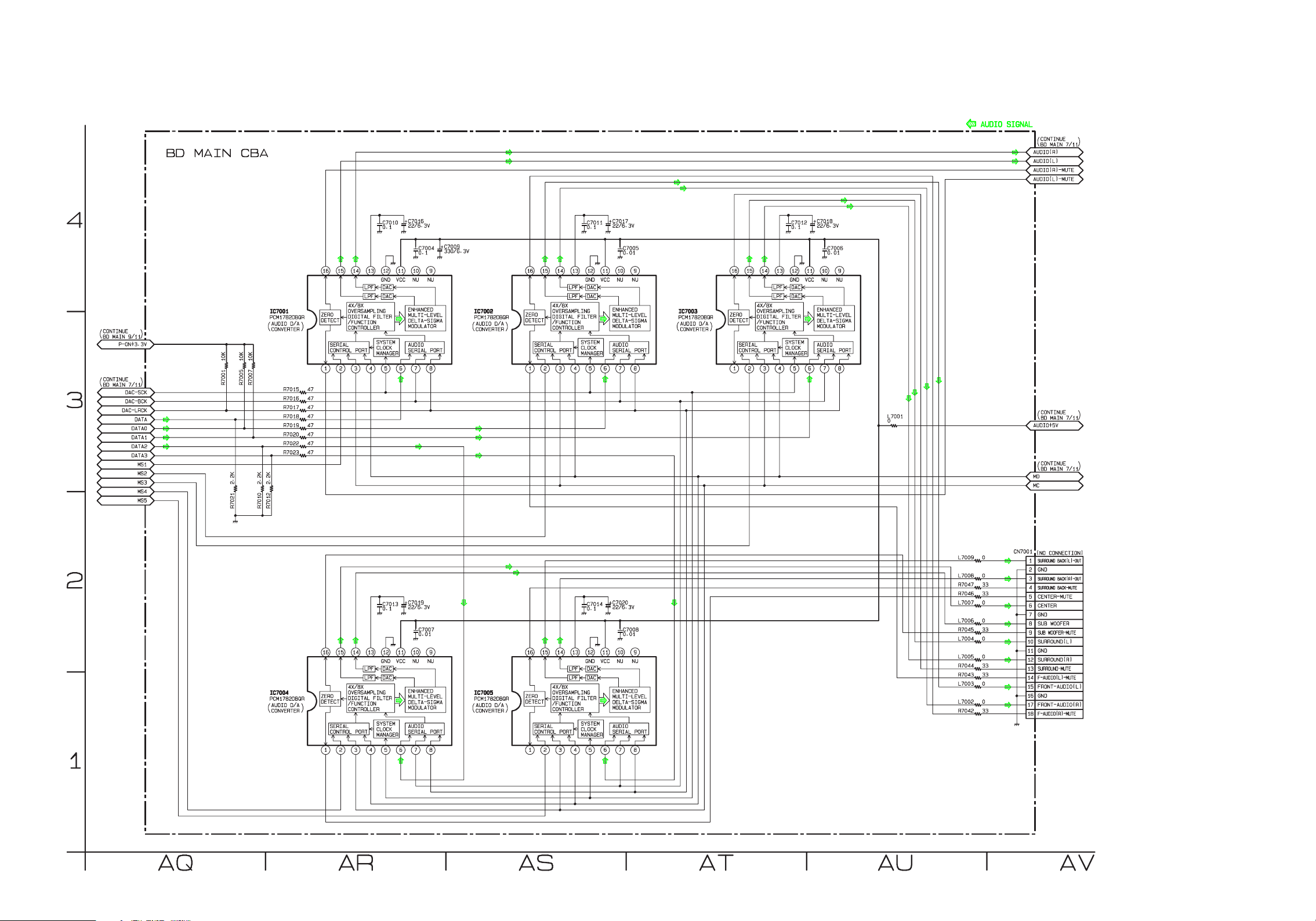
BD Main 8/11 Schematic Diagram
11-25
FL9.5SCBD8
Page 84

BD Main 9/11 Schematic Diagram
1 NOTE:
The order of pins shown in this diagram is different from that of actual IC6001.
IC6001 is divided into nine and shown as IC6001 (1/9) ~ IC6001 (9/9) in this BD Main Schematic Diagram Section.
11-26
FL9.5SCBD9
Page 85

BD Main 10/11 Schematic Diagram
11-27
FL9.5SCBD10
Page 86

BD Main 11/11 Schematic Diagram
1 NOTE:
The order of pins shown in this diagram is different from that of actual IC6001.
IC6001 is divided into nine and shown as IC6001 (1/9) ~ IC6001 (9/9) in this BD Main Schematic Diagram Section.
11-28
FL9.5SCBD11
Page 87

Jack Power CBA Top View
Because a hot chassis ground is present in the power
supply circuit, an isolation transformer must be used.
Also, in order to have the ability to increase the input
slowly,when troubleshooting this type power supply
circuit, a variable isolation transformer is required.
NOTE:
The voltage for parts in hot circuit is measured using
hot GND as a common terminal.
11-29
BA94H0F01012-A
Page 88

Jack Power CBA Bottom View
WF4
PIN 24 OF
CN202
Because a hot chassis ground is present in the power
supply circuit, an isolation transformer must be used.
Also, in order to have the ability to increase the input
slowly,when troubleshooting this type power supply
circuit, a variable isolation transformer is required.
NOTE:
The voltage for parts in hot circuit is measured using
hot GND as a common terminal.
WF3
PIN 22 OF
CN202
WF2
PIN 20 OF
CN202
WF1
PIN 18 OF
CN202
11-30
BA94H0F01012-A
Page 89

Inverter Power CBA Top View
NOTE:
The voltage for parts in hot circuit is measured using
hot GND as a common terminal.
Because a hot chassis ground is present in the power
supply circuit, an isolation transformer must be used.
Also, in order to have the ability to increase the input
slowly,when troubleshooting this type power supply
circuit, a variable isolation transformer is required.
CAUTION !
Fixed voltage (or Auto voltage selectable) power supply circuit is used in this unit.
If Main Fuse (F1601) is blown , check to see that all components in the power supply
circuit are not defective before you connect the AC plug to the AC power supply.
Otherwise it may cause some components in the power supply circuit to fail.
8A 250V
CAUTION ! :
ATTENTION : Utiliser un fusible de rechange de même type de 8A, 250V.
For continued protection against risk of fire,
replace only with same type 8A, 250V fuse.
11-31
BA94H0F01032-A
Page 90

Inverter Power CBA Bottom View
NOTE:
The voltage for parts in hot circuit is measured using
hot GND as a common terminal.
Because a hot chassis ground is present in the power
supply circuit, an isolation transformer must be used.
Also, in order to have the ability to increase the input
slowly,when troubleshooting this type power supply
circuit, a variable isolation transformer is required.
CAUTION !
Fixed voltage (or Auto voltage selectable) power supply circuit is used in this unit.
If Main Fuse (F1601) is blown , check to see that all components in the power supply
circuit are not defective before you connect the AC plug to the AC power supply.
Otherwise it may cause some components in the power supply circuit to fail.
8A 250V
CAUTION ! :
ATTENTION : Utiliser un fusible de rechange de même type de 8A, 250V.
For continued protection against risk of fire,
replace only with same type 8A, 250V fuse.
11-32
BA94H0F01032-A
Page 91

Function CBA Top View
IR Sensor CBA Top View
IR Sensor CBA Bottom View
Function CBA Bottom View
Junction CBA
Top View
BA94H0F01032-C
Junction CBA
Bottom View
11-33
BA94H0F01032-B BA94H0F01012-D
Page 92

BD Power CBA Top View
BD Power CBA Bottom View
11-34
BA94H0F01042-A
Page 93

SD CBA Top View
SD CBA Bottom View
11-35
BA94H0F01042-B
Page 94

WAVEFORMS
CVBS
0.2V
S-VIDEO-Y
0.2V
S-VIDEO-C
0.2V
AUDIO
1V
0.5m
COMPONENT-Pr
0.2V
ms
COMPONENT-Pb
0.2V
COMPONENT-Y
0.2V
WF1 ~ WF4 = Waveforms to be observed at
Waveform check points.
(Shown in Schematic Diagram.)
Input: NTSC Color Bar Signal (with 1kHz Audio Signal)
WF1
Pin 18 of CN202
(VIDEO IN)
CVBS
0.2V
(S-VIDEO IN)
S-VIDEO-Y
0.2V
(COMPONENT IN)
2020m
s
2020m
s
WF3
Pin 22 of CN202
(S-VIDEO IN)
S-VIDEO-C
0.2V
(COMPONENT IN)
COMPONENT-Pr
0.2V
2020m
2020ms
s
COMPONENT-Y
WF2
Pin 20 of CN202
COMPONENT-Pb
0.2V
0.2V
2020m
s
2020m
s
WF4
AUDIO
Pin 24 of CN202
1V
0.5m
s
FL9.5WF12-1
Page 95

Wiring 1/2 Diagram
4
2
3
1
WH1301BWH1301A
CL1301
KEY-IN2
GND
KEY-IN1
AL+3.3V
4
2
3
1
WH1302B
8
6
7
5
4
3
2
1
GND
REMOTE
LED1
P-ON-H1
KEY-IN1
KEY-IN2
4
5
4
5
LED1
P-ON-H1
4
5
CN902
3 HOT+22V
CL902
4HOT+22V
CN1802
1PANEL+24V
CN1803
CL1803
DVD-LED
6
7
8
6
7
8
KEY-IN1
KEY-IN2
DVD-LED
6
7
8
1
2
AL+5V
AL+5V
23
22
4PANEL+24V
3PANEL+24V
2PANEL+24V
WH1302A
CN1302 CL1302
CN203
CN1501
CN1601
AC
INLET
1
2
1
2
GND
REMOTE
1
2
CN601
1 +345V
2NU
1+345V
2
1
CL1601
3 AL+3.3V
3
3 AL+3.3V
2 HOT-GND
3HOT-GND
JUNCTION CBA IR SENSOR CBA FUNCTION CBA
3
4
P-ON-H2
21 P-ON-H1
20
6GND
5PANEL+24V
SP801
SPEAKER
1
2
SP(L)-
CN801
SP(L)+
5
6
7
8
POWER-RESET
GND
BACKLIGHT-ADJ
BACKLIGHT-SW
19
18
17
16
INVERTER
POWER CBA
9GND
8GND
7GND
WIRING DIAGRAM
9GND
10GND
CL203
1
2
3
4
5
6
7
8
9
10
11
12
13
14
15
16
17
18
19
20
21
22
23
24
25
26
27
28
29
1
2
3
4
5
6
7
8
9
10
11
12
13
14
15
16
17
18
19
20
21
22
23
24
25
26
27
28
29
S-VIDEO
-IN1
S-VIDEO
-IN2
VIDEO
-IN1
AUDIO(L)
-IN1
AUDIO(R)
-IN1
VIDEO
-IN2
AUDIO(L)
-IN2
AUDIO(R)
-IN2
AUDIO(L)
-OUT
AUDIO(R)
-OUT
DIGITAL
-AUDIO-OUT
COMPONENT
-AUDIO(L)-IN2
COMPONENT
-AUDIO(R)-IN2
COMPONENT
-Y-IN2
COMPONENT
-Pb-IN2
COMPONENT
-Pr-IN2
HDMI
-AUDIO(L)-IN
HDMI
-AUDIO(R)-IN
L-CH
CN802
9
10
GND
PROTECT3
14
15
11PROTECT3
10GND
12NU
SP802
SPEAKER
R-CH
1
2
SP(R)-
SP(R)+
11
12
DVD-P-ON2
DVD-P-ON1
13
12
14
13
BACKLIGHT-SW
BACKLIGHT-ADJ
13
14
15
16
IREDCONTV
DISC-OUT
DISC-IN
DVD-SPDIF
9
8
11
10
1PANEL+24V
CN1804
CL1804
17
18
GND
SUB-RXD
7
6
3PANEL+24V
2PANEL+24V
TUNER UNIT
19
20
21
SUB-TXD
DVD-RESET
DVD-READY
5
4
3
7GND
6GND
5PANEL+24V
4PANEL+24V
JACK POWER CBA
22
PROTECT4
2
1GND
2KEY-IN2
3DVD-LED
4GND
5DVD-P-ON2
6DVD-P-ON1
7IREDCONTV
8DISC-OUT
9DISC-IN
10DVD-SPDIF
11GND
12SUB-RXD
13SUB-TXD
14DVD-RESET
15DVD-READY
16PROTECT4
17GND
8GND
CN903
23
GND
1
CL202
REMOTE
LED1
KEY-IN1
AUDIO(L)-OUT
GND
AUDIO(R)-OUT
GND
AMP(L)-OUT
GND
AMP(R)-OUT
AUDIO-MUTE
GND
SPDIF
GND
AL+3.3V
AL+3.3V
GND
CVBS/Y/S-Y-IN
GND
Pb-IN
GND
Pr/S-C-IN
GND
AUDIO(L)
GND
AUDIO(R)
SDA
SCL
GND
CL201
IF-AGC
GND
DIF-OUT1
DIF-OUT2
GND
P-ON-H2
PROTECT3
P-ON-H1
PROTECT2
PROTECT1
RESET
GND
GND
P-ON+5V
P-ON+3V
P-ON+3V
GND
P-ON+7V
GND
GND
P-ON+3.3V
P-ON+3.3V
BACKLIGHT-SW
GND
BACKLIGHT-ADJ
GND
LCD+12V
LCD+12V
LCD+12V
CN4001
1 GND
2 KEY-IN2
3 DVD-LED
4 GND
5 DVD-P-ON2
6 DVD-P-ON1
7 IREDCONTV
8 DISC-OUT
9 DISC-IN
10 DVD-SPDIF
11 GND
12 SUB-RXD
13 SUB-TXD
14 DVD-RESET
15 DVD-READY
16 PROTECT4
17 GND
CN3702CN202
1
2
3
4
5
6
7
8
9
10
11
12
13
14
15
16
17
18
19
20
21
22
23
24
25
26
27
28
29
CN3701CN201
1
2
3
4
5
6
7
8
9
10
11
12
13
14
DIGITAL MAIN CBA UNIT
15
16
17
18
19
20
21
22
23
24
25
26
27
28
29
HDMI-
CONNECTOR
CN3902
1 USB+5V
2
3
4
1
2
3
4
5
6
7
8
9
10
11
12
13
14
15
16
17
18
19
20
21
22
23
24
25
26 NU
27 NU
28 NU
29 LVDS-D3O(+)
30 LVDS-D3O(-)
31 GND
32 LVDS-CO(+)
33 LVDS-CO(-)
34 GND
35 LVDS-D2O(+)
36 LVDS-D2O(-)
37 LVDS-D1O(+)
38 LVDS-D1O(-)
39 LVDS-D0O(+)
40 LVDS-D0O(-)
41 NU
42 NU
43 GND
44 P-ON+3.3V
45 NU
46 NU
47 NU
48 NU
49 NU
50 NU
51 NU
HDMICONNECTOR-1
HDMICONNECTOR-2
HDMICONNECTOR-3
CL3804
(TO BD MAIN CBA)
USB(-)
USB(+)
GND
CL3901CN3901
LCD+12V
LCD+12V
LCD+12V
LCD+22V
GND
GND
GND
GND
NU
NU
NU
NU
LVDS-D3E(+)
LVDS-D3E(-)
GND
LVDS-CE(+)
LVDS-CE(-)
GND
LVDS-D2E(+)
LVDS-D2E(-)
LVDS-D1E(+)
LVDS-D1E(-)
LVDS-D0E(+)
LVDS-D0E(-)
NU
USB JACK
LCD MODULE ASSEMBLY
AC CORD
AC601
13-1
FL9.5WI1
Page 96

Wiring 2/2 Diagram
*1 LD427SSX
42MD459B/F7 (Serial No. : YA2A**********)
*2 42MD459B/F7 (Serial No. :DS1A**********)
CL1902
CN1902 CN2402
+12V
+10.5V
+10.5V
GND
GND
GND
IREDCONTV
AL+3.3V
DISC-OUT
DISC-IN
FAN-GND
FAN-POWER
INVERTER POWER CBA
CL1901
CN1901 CN2401
PROTECT4
DVD-P-ON1
DVD-P-ON2
GND
GND
+5V
+5V
GND
DVD-SPDIF
GND
SUB-RXD
SUB-TXD
DVD-RESET
DVD-READY
FAN-POWER
FAN
FAN-GND
SD CARD SLOT
*2CL1901
*1
11
22
33
44
55
66
77
88
99
1010
1111
1212
11
22
33
44
55
66
77
88
99
1010
1111
1212
1313
1414
CN2501
1
2
CN2801 CN7601
GND
1
WP
2
CD
3
SDDAT1
4
GND
5
SDDAT0
6
GND
7
SDCLK
8
D+3.3V
9
SD CBA
BD POWER CBA
D+3.3V
10
GND
11
CMD
12
GND
13
SDDAT3
14
GND
15
SDDAT2
16
CL2103
CN2103
DISC-IN
DISC-OUT
GND
AL+3.3V
IREDCONTV
CN2102
CL2102
GND
1
NU
2
AUDIO+5V
3
AUDIO+5V
4
SPDIF
5
GND
6
SUB-RXD
7
SUB-TXD
8
SYS-RESET
9
RDY
10
GND
11
NU
12
GND
13
NU
14
GND
15
NU
16
GND
17
NU
18
GND
19
NU
20
GND
21
NU
22
GND
23
NU
24
NU
25
NU
26
CN2101 CN6001
P-ON+5V(2)
23
GND
22
GND
21
P-ON+1.2V
20
P-ON+1.2V
19
P-ON+1.2V
18
P-ON+1.2V
17
GND
16
GND
15
GND
14
GND
13
GND
12
P-ON+1.8V
11
P-ON+1.8V
10
P-ON+1.8V
9
GND
8
GND
7
P-ON+3.3V
6
P-ON+3.3V
5
P-ON+10.5V
4
P-ON+10.5V
3
P-ON+5V(1)
2
USB+5V
1
1
2
3
4
5
6
7
8
9
10
11
12
13
14
15
16
CN501
51
42
33
24
15
CN7101
1
2
3
4
5
6
7
8
9
10
11
12
13
14
15
16
17
18
19
20
21
22
23
24
25
26
23
22
21
20
19
18
17
16
15
14
13
12
11
10
9
8
7
6
5
4
3
2
1
BD MAIN CBA
CN602
CN101
FD1
FR1
FR2
FD2
EXPA(-)
EXPB(-)
EXPA(+)
EXPB(+)
SA-INT
PI-CONT
GND
BDRF(+)
BDRF(-)
GND
RF(+)
RF(-)
GND
+5V
VC-PD
GND
GND
+3.3V
GND
GND
+5V
+8V
THERMO
SCLK2
SEN-LDD
SDATA2
XRESET
LDEN
NU
TEST-V
NU
CN601
SLD1(-)
SLD1(+)
SLD2(-)
SLD2(+)
CN603
+5V
HU(+)
HU(-)
HV(+)
HV(-)
HW(+)
HW(-)
HB(-)
DISC-OUT
LOAD(+)
CLAMPSW
LED-POW
TD
TR
A
B
C
D
E
F
G
H
W
V
U
DISC-IN
INLIMIT
LOAD(-)
CL3804
HDMI-CONNECTOR
(TO DIGITAL MAIN CBA)
1
2
3
4
5
6
7
8
9
10
11
12
13
14
15
16
17
18
19
20
21
22
23
24
25
26
27
28
29
30
31
32
33
34
35
36
37
38
39
40
41
42
43
44
45
1
2
3
4
1
2
3
4
5
6
7
8
9
10
11
GND
11
22
33
44
55
66
77
88
CD/DVD
RELAY CBA
PICKUP
LENS DRIVE
-OEIC
BD-OEIC
BD-LD
CD-LD
PD-LD
DVD-LD
LASER DIODE DRIVE
M
SLED
MOTOR
M
SPINDLE
MOTOR
CLAMP
INNER
M
BD MAIN CBA & BD MECHANISM ASSEMBLY
SW
SW
LOADING
MOTOR
13-2
FL9.5WI2
Page 97

SYSTEM CONTROL TIMING CHARTS
Power on
SLED moves
Start
SLED position
initialization
Pick-up position
moves
Power on
SLED moves
End
Hand close
Start
Hand close
detection
Disc
Loading
SLED position
initialization
Pick-up position
moves
Hand Close
End
Eject
Start
SLED inner
around moves
Disc eject
Eject
End
14-1 LC7BD_TI
Page 98
Parameter
V*: Voltage T*: Event timer
V0: 3.5 V T0: 4.0 s
V1: 3.7 V T1: 0.2 s
V2: 3.5 V T2: 4.0 s
V3: 4.0 V T3: 0.2 s
T4: 0.5 s
T5: 4.0 s
Disc-in-sw
Disc-out-sw
Clump-sw
Disc-out direction
Motor voltage 0[V]
Disc-in direction
off
on
off
on
off
on
V0
Disc Out
Till Disc-out-sw
becomes ON.
Time-out (T0) Time-out (T2)
Brake mode (T1)
V1
V2
Time-out (T5)
0[V]
Disc In
Till Clump-sw
becomes ON.
Till Clump-sw
becomes ON.
Brake mode (T3)
T4
V3
14-2 LC7BD_TI
Page 99

LEAD IDENTIFICATIONS
ECB
PQ070XF01SZH
1234
KTA1267-GR-AT/P
KTC3199-GR-AT/P
1: Vin
2: Vout
3: GND
4: Vadj
ECB
2SA950-O(TE2 F T)
2SC2120-O(TE2 F T)
2SC5344O-AT
KTA1271-O-AT/P
KTC3198-Y-AT/P
LTV-817MBF
LTV-817MCF
1
2
1: A
4
2: K
3
3: E
4: C
2SK3561(Q)
2SK3757(Q)
2SK3798(Q.M)
GDS BCE
2SA1931(Q)
2SC4881F
BD9322EFJ-E2
BD9323EFJ-E2
BD9324EFJ-E2
NJM4558M(TE1)
8
1
5
4
TEA1611T/N1.518
20
1
UCC28060DR
16
1
11
10
BD5426EFS-E2
44
1
23
22
BH7645KS2
39
27
Note:
9
40
26
A: Anode
K: Cathode
E: Emitter
C: Collector
B: Base
R: Reference
52
14
8
1
13
S: Source
G: Gate
D: Drain
15-1 FL9.5LE
Page 100

EXPLODED VIEWS
Cabinet [LD427SSX (Serial No. : DS1A**********), 42MD459B/F7 (Serial No. : DS1A**********)]
Comparison Chart of Models and Marks
Model Mark
LD427SSX
42MD459B/F7
L1
L1
L4
L1
L3
L6
CL1601
B1
B19
L3
L4
L4
A
B
CL902
L3
Digital Main CBA Unit
B24
L3
L8
B20
L12
L4
L12
B17
L3
A1
A21
B28
A7
A29
CL1301
L4
L3
X2803
BD Main CBA &
BD Mechanism Assembly
Function CBA
A5
B28
CL1302
IR Sensor CBA
B15
L4
L4
See Electrical Parts List
for parts with this mark.
L3
L2
B12
SD CBA
CL2103
B16
L3
B11
CL802
SP802
B10
L1
LCD-1
L3
B28
L2
B28
Junction CBA
L1
[ B ]
CL3804
CL2102
L3
X2501
L9
L6
B27
L3
B12
SP801
B10
CL1901
L3
B25
B11
CL801
L1
L1
CL1804
L4
[ A ]
B24
CL1803
B2
L3
L6
CL1901
CL1902
BD Power CBA
L1
B9
B14
L3
B18
Inverter Power CBA
L4
B3
Jack Power CBA
L4
L3
CL3901
L3
B23
L8
L8
L8
CL201
CL202
B5
CL203
B22
B21
B28
A10
B24
L3
X3301
L8
L2
A14
B21
B13
B26
L8
B13
B4
L1
B6
L5
L1
AC601
L5
A4
X5
L1
L6
L1
L7
L5
A8
S5
A6
Stand Assembly
16-1 FL9.5-1CEX
 Loading...