MagnaChip HMS87C1808B, HMS87C1708B, HMS87C1608B, HMS87C1508B, HMS87C1404B User Manual
...
查询HMS87C1404B供应商
MAGNACHIP SEMICONDUCTOR LTD.
8-BIT SINGLE-CHIP MICROCONTROLLERS
HMS87C1808B/16B
HMS87C1708B/16B
HMS87C1608B/16B
HMS87C1508B/16B
HMS87C1404B/08B/16B
User’s Manual (Ver. 1.03)

REVISION HISTORY
VERSION 1.03 (SEP. 2004) This book
The company name, Hynix Semiconductor Inc. changed to MagnaChip Semiconductor Ltd.
VERSION 1.02 (MAR. 2004)
Correct the external RC oscillation characteristics
Fixed some errata.
VERSION 1.01 (MAY. 2003)
Fixed some errata.
Version 1.03
Published by
MCU Application Team
2004 MagnaChip Semiconductor Ltd. All right reserved.
Additional information of this manual may be served by MagnaChip Semiconductor offices in Korea or Distributors and Representatives.
MagnaChip Semiconductor reserves the right to make changes to any information here in at any time without notice.
The information, diagrams and other data in this manual are correct and reliable; however, MagnaChip Semiconductor is in no way responsible for any violations of patents or other rights of the third party generated by the use of this manual.

HMS87C1X04B/08B/16B
1. OVERVIEW .........................................................1
Description .........................................................1
Features .............................................................1
Development Tools ............................................2
Ordering Information ...................................3
2. BLOCK DIAGRAM .............................................4
3. PIN ASSIGNMENT .............................................5
4. PACKAGE DRAWING ........................................7
5. PIN FUNCTION .................................................10
6. PORT STRUCTURES .......................................12
7. ELECTRICAL CHARACTERISTICS ................17
Absolute Maximum Ratings .............................17
Recommended Operating Conditions ..............17
A/D Converter Characteristics .........................17
DC Electrical Characteristics ...........................18
AC Characteristics ...........................................19
Typical Characteristics .....................................20
8. MEMORY ORGANIZATION .............................23
Registers ..........................................................23
Program Memory .............................................25
Data Memory ...................................................28
Addressing Mode .............................................32
9. I/O PORTS ........................................................36
RA and RAIO registers ....................................36
RB and RBIO registers ....................................37
RC and RCIO registers ....................................39
RD and RDIO registers ....................................40
RE and REIO registers ....................................40
10. CLOCK GENERATOR ...................................41
Oscillation Circuit .............................................41
11. Basic Interval Timer .....................................43
12. TIMER / COUNTER ........................................44
8-bit Timer/Counter Mode ............................... 45
16-bit Timer/Counter Mode ............................. 46
8-bit Compare Output (16-bit) ......................... 47
8-bit Capture Mode ......................................... 47
16-bit Capture Mode ....................................... 50
PWM Mode ..................................................... 50
13. Serial Peripheral Interface ........................... 53
14. Buzzer Output function ................................ 55
15. ANALOG TO DIGITAL CONVERTER ........... 56
16. INTERRUPTS ................................................ 59
Interrupt Sequence .......................................... 61
BRK Interrupt .................................................. 62
Multi Interrupt .................................................. 62
External Interrupt ............................................. 64
17. WATCHDOG TIMER ...................................... 66
18. Power Saving Mode ..................................... 67
Stop Mode ....................................................... 67
STOP Mode using Internal RCWDT ............... 69
Wake-up Timer Mode ...................................... 70
Minimizing Current Consumption .................... 71
19. RESET ........................................................... 73
20. POWER FAIL PROCESSOR ......................... 75
21. COUNTERMEASURE OF NOISE ................. 77
Oscillation Noise Protector .............................. 77
Oscillation Fail Processor ................................ 78
Device Configuration Area .............................. 78
Examples of ONP ............................................ 79
22. OTP PROGRAMMING ................................... 80
EPROM Mode ................................................. 80
23. APPENDIX ........................................................ i
A. INSTRUCTION MAP ......................................i
B. INSTRUCTION SET ......................................ii
SEP. 2004 Ver 1.03


HMS87C1X04B/08B/16B
HMS87C1808B / 16B
HMS87C1708B / 16B
HMS87C1608B / 16B
HMS87C1508B / 16B
HMS87C1404B / 08B / 16B
CMOS SINGLE-CHIP 8-BIT MICROCONTROLLER
1. OVERVIEW
1.1 Description
The HMS87C1X04B/08B/16B is an advanced CMOS 8-bit microcontroller with 4K/8K/16K bytes of ROM. The MagnaChip semiconductor’s HMS87C1X04B/08B/16B is a powerful microcontroller which provides a highly flexible and cost effective solution to many embedded control applications. The HMS87C1X04B/08B/16B provides the following standard features: 4K/8K/16K bytes of ROM, 448
bytes of RAM, 8-bit timer/counter, 8-bit A/D converter, 10-bit high speed PWM output, programmable buzzer driving port, 8-bit serial
communication port, on-chip oscillator and clock circuitry. In addition, the HMS87C1X04B/08B/16B support power saving modes to reduce power consumption.
This document is only explained for the base HMS87C1816B, the other’s eliminated functions are same as below.
Device name EPROM RAM EXT.INT BUZ
HMS87C14XXB 4,8,16K bytes
HMS87C15XXB
HMS87C16XXB 35 40 PDIP
HMS87C17XXB 37 42 SDIP
HMS87C18XXB 39 44 QFP
8,16K bytes
448bytes 4 O 2.3 ~ 5.5V
Operating
Voltage
I/O Package
23 28 SKDIP or SOP
27 32 PDIP
1.2 Features
• 4K/8K/16 Bytes On-chip Program Memory
• 448 Bytes of On-chip Data RAM
(Included stack memory)
• Instruction Cycle Time:
- 250nS at 8MHz
• Programmable I/O pins
(LED direct driving can be source and sink)
- HMS87C14XXB : 23
- HMS87C15XXB : 27
- HMS87C16XXB : 35
- HMS87C17XXB : 37
- HMS87C18XXB : 39
• Operating Voltage & Frequency
- 2.3V ~ 5.5V (at 1 ~ 4.2MHz)
- 4.5V ~ 5.5V (at 1 ~ 8.0MHz)
• Eight 8-bit A/D Converter
• Four External Interrupt Ports.
• One 8-bit Basic Interval Timer
• Four 8-bit Timer / Counters
• Two 10-bit High Speed PWM Outputs
• Watchdog timer (can be operate with internal
RC-oscillation)
• One 8-bit Serial Peripheral Interface
• Twelve Interrupt sources
- External input: 4
- A/D Conversion: 1
SEP. 2004 Ver 1.03 1
HMS87C1X04B/08B/16B
- Serial Peripheral Interface: 1
- Timer: 6
• One Programmable Buzzer Driving port
- 500Hz ~ 130kHz
• Noise Immunity Circuit
- Power Fail Processor
- Oscillation Noise Protector
- Oscillation Fail Processor
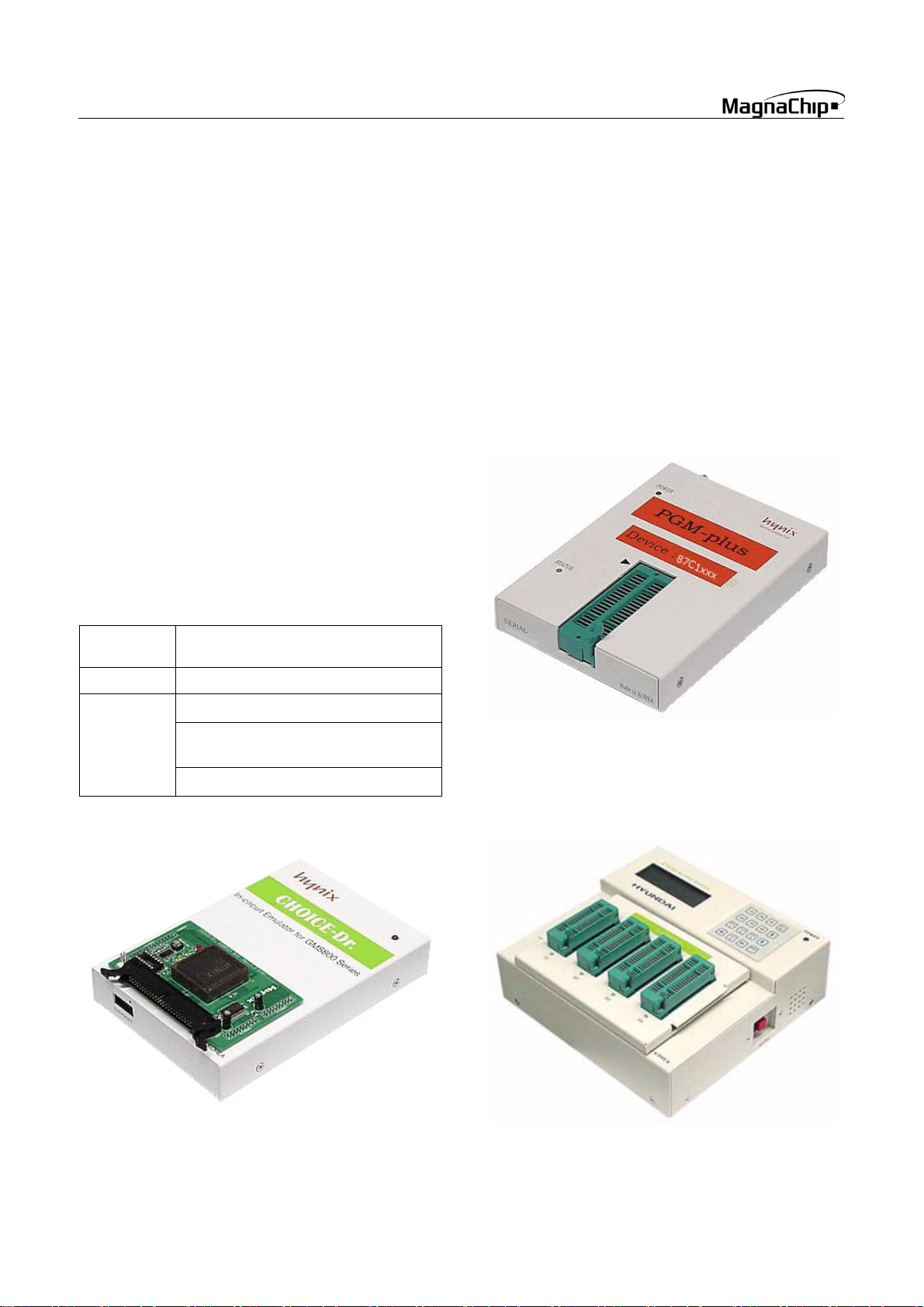
1.3 Development Tools
The HMS87C1X04B/08B/16B is supported by a full-featured
macro assembler, C compiler and an in-circuit emulator
CHOICE-Dr
The macro assembler and C compiler operate under the MS-Windows 95/98, 2000, XPTM.
The OTP programmer can be supplied three types of programmer
such as emulator add-on board type single programmer (PGMplus
(CHOICE-SIGMATM) and gang type programmer (CHOICEGANG4TM).
TM
and OTP programmers.
TM
), universal stand-alone type single programmer
• Oscillator Type
- Crystal
- Ceramic Resonator
- RC Oscillator ( C can be omitted )
- Internal Oscillator ( approx. 4MHz )
• Power Down Mode
- STOP mode
- Wake-up Timer mode
In Circuit
Emulators
Assembler
OTP
Programmer
CHOICE-Dr.
MagnaChip Macro Assembler
Single Programmer : PGM-plus
Universal Programmer : CHOICE-
SIGMA
Gang Programmer : CHOICE-GANG4
TM
TM
TM
TM
Figure 1-2 OTP Single Programmer PGM-plus
TM
Figure 1-1 In Circuit Emulator CHOICE-Dr.
TM
Figure 1-3 OTP Gang Programmer CHOICE-GANG4
TM
2 SEP. 2004 Ver 1.03

1.4 Ordering Information
ROM Size Package Type Ordering Device Code Operating Temperature
4K bytes (OTP) 28 SKDIP HMS87C1404B SK
8K bytes (OTP)
16K bytes (OTP)
28 SOP HMS87C1404B D
28 SKDIP HMS87C1408B SK
28 SOP HMS87C1408B D
32 PDIP HMS87C1508B
40 PDIP HMS87C1608B
42 SDIP HMS87C1708B K
44 MQFP HMS87C1808B Q
28 SKDIP HMS87C1416B SK
28 SOP HMS87C1416B D
32 PDIP HMS87C1516B
40 PDIP HMS87C1616B
42 SDIP HMS87C1716B K
44 MQFP HMS87C1816B Q
HMS87C1X04B/08B/16B
-40 ~ +85°C
SEP. 2004 Ver 1.03 3
HMS87C1X04B/08B/16B
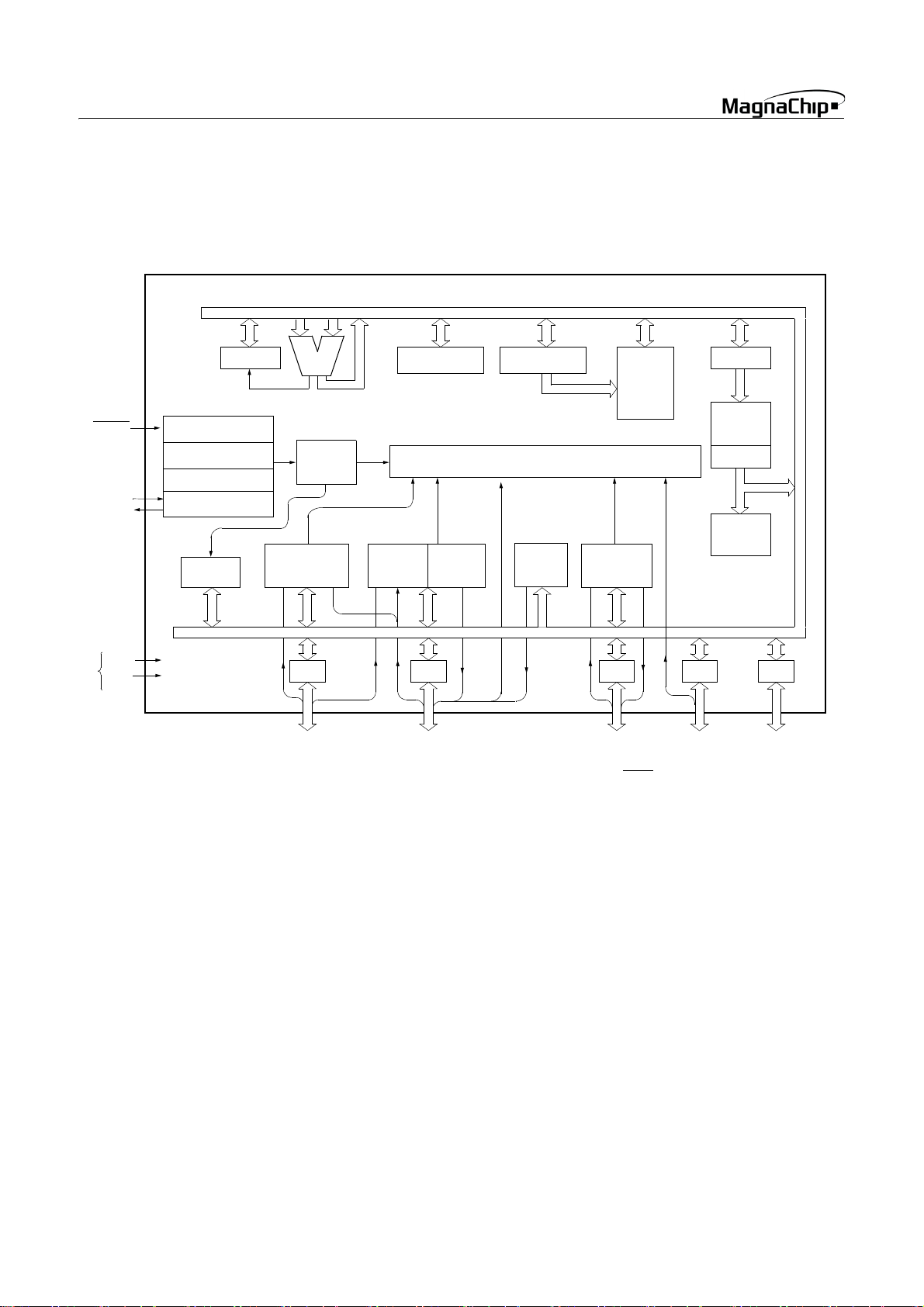
2. BLOCK DIAGRAM
RESET
Xin
Xout
V
DD
V
SS
Power
Supply
PSW
System controller
System
Clock Controller
Timing generator
Clock Generator
Watch-dog
Timer
ALU
8-bit Basic
Interval
Timer
8-bit
A/D
Converter
RA RB RC
RA0 / EC0
RA1 / AN1
RA2 / AN2
RA3 / AN3
RA4 / AN4
RA5 / AN5
RA6 / AN6
RA7 / AN7
Accumulator Stack Pointer
8-bit
Timer/
Counter
High
Speed
PWM
RB0 / AN0 / Avref
RB1 / BUZ
RB2 / INT0
RB3 / INT1
RB4 / CMP0 / PWM0
RB5 / CMP1 / PWM1
RB6 / EC1
RB7 / TMR2OV
Interrupt Controller
Buzzer
Driver
Data
Memory
SPI
RC0
RC1
RC2
RC3 / SRDY
RC4 / SCK
RC5 / SIN
RC6 / SOUT
RC7
PC
Program
Memory
Data Table
Instruction
Decoder
RD
RD0 / INT2
RD1 / INT3
RD2
RD3
RD4
RD5
RD6
RD7
RE
RE0
RE1
RE2
RE3
RE4
RE5
RE6
RE7
4 SEP. 2004 Ver 1.03
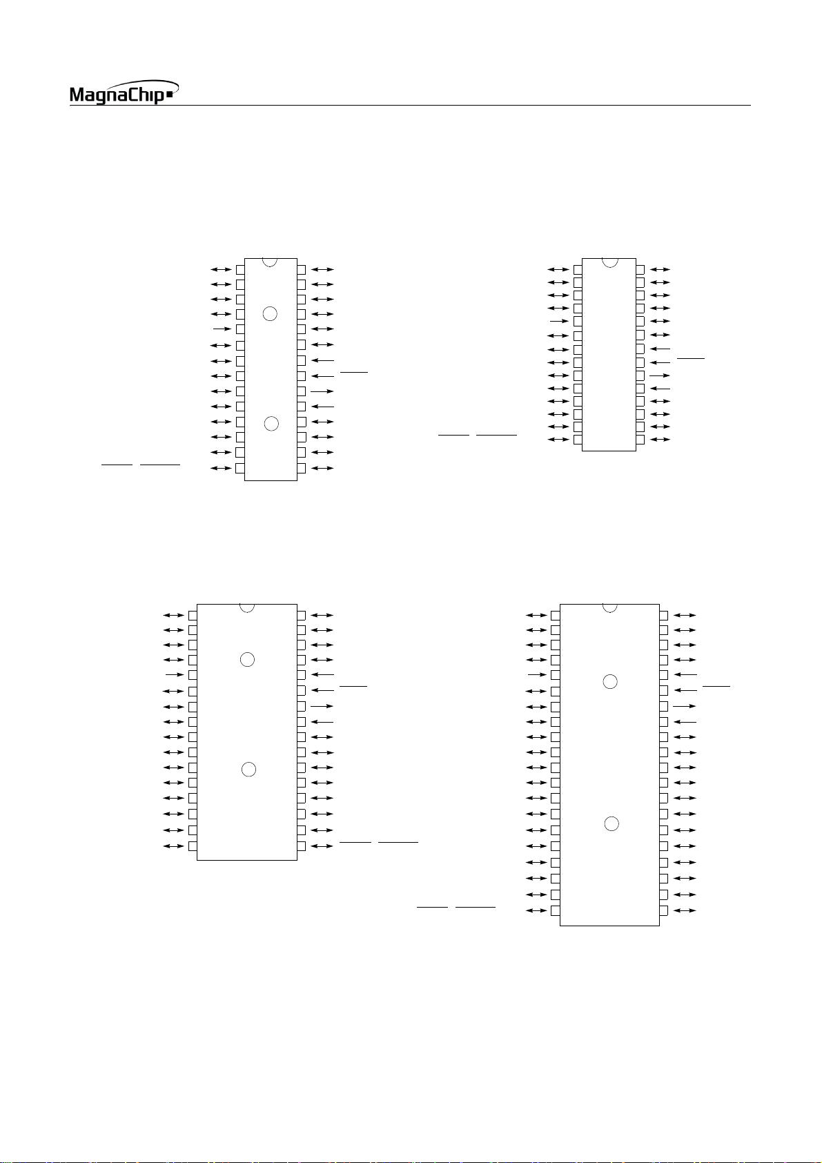
3. PIN ASSIGNMENT
HMS87C1X04B/08B/16B
HMS87C14XXB SK
AN5 / RA5
AN6 / RA6
AN7 / RA7
V
DD
AN0 / AV
PWM0 / COMP0 / RB4
PWM1 / COMP1 / RB5
SRDYIN / SRDYOUT / RC3
/ RB0
REF
BUZ / RB1
INT0 / RB2
INT1 / RB3
EC1 / RB6
TMR2OV / RB7
HMS87C15XXB
HMS87C14XXB D
28 SKDIP
2
27
3
26
4
25
5
24
23
6
22
7
8
21
9
20
10
19
11
18
12
17
13 16
14 15
RA3 / AN3AN4 / RA4 1 28
RA2 / AN2
RA1 / AN1
RA0 / EC0
RD1 / INT3
RD0 / INT2
V
SS
RESET
X
OUT
X
IN
RD2
RC6 / SOUT
RC5 / SIN
RC4 / SCK
AN4 / RA4
AN5 / RA5
AN6 / RA6
AN7 / RA7
V
AN0 / AV
PWM0 / COMP0 / RB4
PWM1 / COMP1 / RB5
SRDYIN / SRDYOUT / RC3
/ RB0
REF
BUZ / RB1
INT0 / RB2
INT1 / RB3
EC1 / RB6
TMR2OV / RB7
DD
28 SOP
1
28
2
27
3
26
4
25
5
24
23
6
22
7
8
21
9
20
10
19
11
18
12
17
13
16
14
15
HMS87C16XXB
32 PDIP 40 PDIP
RA3 / AN3
RA2 / AN2
RA1 / AN1
RA0 / EC0
RD1 / INT3
RD0 / INT2
V
SS
RESET
X
OUT
X
IN
RD2
RC6 / SOUT
RC5 / SIN
RC4 / SCK
AN4 / RA4
AN5 / RA5
AN6 / RA6
AN7 / RA7
V
AN0 / AV
PWM0 / COMP0 / RB4
PWM1 / COMP1 / RB5
/ RB0
REF
BUZ / RB1
INT0 / RB2
INT1 / RB3
EC1 / RB6
TMR2OV / RB7
RC0
RC1
RC2
1
2
3
4
DD
5
6
7
8
9
10
11
12
13
14
15
16
31
30
29
28
27
26
25
24
23
22
21
20
19
17
RA3 / AN332
RA2 / AN2
RA1 / AN1
RA0 / EC0
V
SS
RESET
X
OUT
X
IN
RD2
RD1 / INT3
RD0 / INT2
RC7
RC6 / SOUT
RC5 / SIN
RC4 / SCK18
SRDYIN / SRDYOUT / RC3
SRDYIN / SRDYOUT / RC3
AN4 / RA4
AN5 / RA5
AN6 / RA6
AN7 / RA7
V
AN0 / AV
PWM0 / COMP0 / RB4
PWM1 / COMP1 / RB5
/ RB0
REF
BUZ / RB1
INT0 / RB2
INT1 / RB3
EC1 / RB6
TMR2OV / RB7
RE2
RE1
RE0
RC0
RC1
RC2
1
2
3
4
DD
5
6
7
8
9
10
11
12
13
14
15
16
17
18
19
20
39
38
37
36
35
34
33
32
31
30
29
28
27
25
23
21
RA3 / AN340
RA2 / AN2
RA1 / AN1
RA0 / EC0
V
SS
RESET
X
OUT
X
IN
RD7
RD6
RD5
RD4
RD3
RD2
RD1 / INT326
RD0 / INT2
RC724
RC6 / SOUT
RC5 / SIN22
RC4 / SCK
SEP. 2004 Ver 1.03 5

HMS87C1X04B/08B/16B
HMS87C17XXB K
HMS87C18XXB Q
AN4 / RA4
AN5 / RA5
AN6 / RA6
AN7 / RA7
AN0 / AV
PWM0 / COMP0 / RB4
PWM1 / COMP1 / RB5
TMR2OV / RB7
V
/ RB0
REF
BUZ / RB1
INT0 / RB2
INT1 / RB3
EC1 / RB6
RE4
RE3
RE2
RE1
RE0
RC0
RC1
RC2
42 SDIP
1
2
3
4
DD
5
6
7
8
9
10
11
12
13
14
15
16
17
18
19
20
21
42
41
40
39
38
37
36
35
34
33
32
31
30
29
28
27
26
25
24
23
22
RA3 / AN3
RA2 / AN2
RA1 / AN1
RA0 / EC0
V
SS
RESET
X
OUT
X
IN
RD7
RD6
RD5
RD4
RD3
RD2
RD1 / INT3
RD0 / INT2
RC7
RC6 / SOUT
RC5 / SIN
RC4 / SCK
SRDYIN / SRDYOUT / RC3
44 MQFP
AN0 / AV
V
RA0 / EC0
RA1 / AN1
RA2 / AN2
RA3 / AN3
AN4 / RA4
AN5 / RA5
AN6 / RA6
AN7 / RA7
V
/ RB0
REF
OUTXIN
RESET
X
RD7
RD6
SS
DD
3332313029282726252423
34
35
36
37
38
39
40
41
42
43
44
1234567891011
BUZ / RB1
INT0 / RB2
INT1 / RB3
PWM0 / COMP0 / RB4
PWM1 / COMP1 / RB5
RD5
EC1 / RB6
RD4
TMR2OV / RB7
RD3
RE6
RD2
RE5
RD1 / INT3
RE4
RD0 / INT2
22
21
20
19
18
17
16
15
14
13
12
RE3
RC7
RC6 / SOUT
RC5 / SIN
RC4 / SCK
SRDYIN / SRDYOUT / RC3
RC2
RC1
RC0
RE0
RE1
RE2
6 SEP. 2004 Ver 1.03
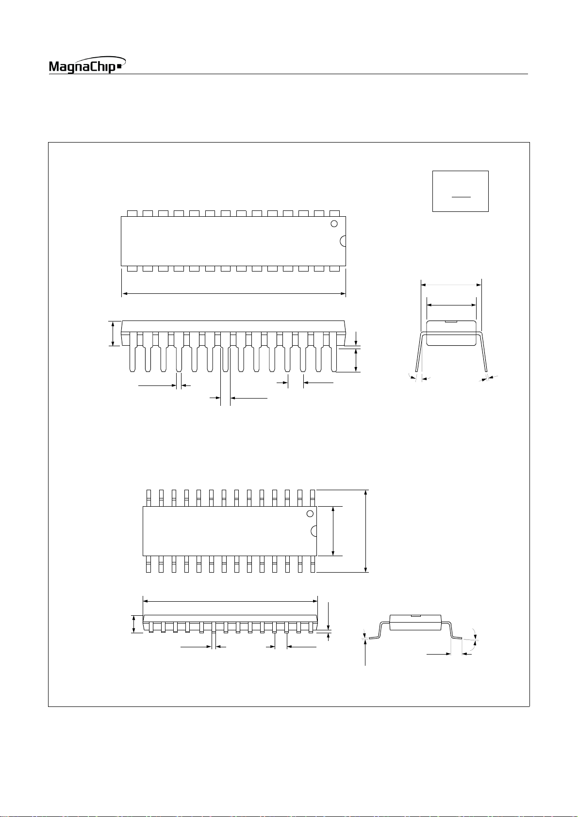
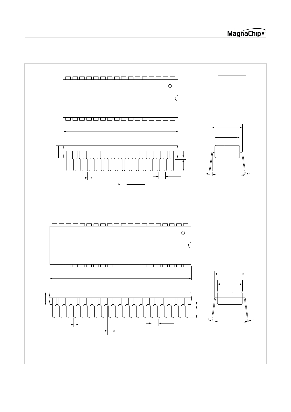
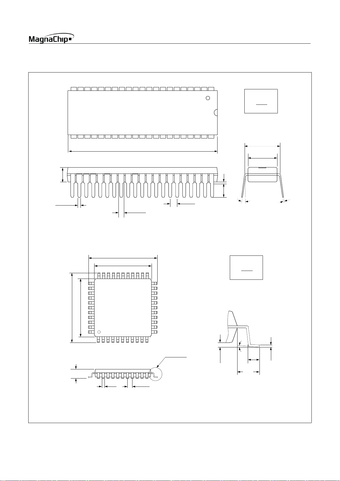
4. PACKAGE DRAWING
HMS87C1X04B/08B/16B
28 SKINNY DIP
MAX 0.180
0.021
0.015
1.375
1.355
0.055
0.045
TYP 0.100
0.140
MIN 0.020
0.120
0 ~ 15°
unit: inch
MAX
MIN
TYP 0.300
0.300
0.275
4
1
0
.
0
8
0
0
.
0
28 SOP
0.104
0.093
0.020
0.0138
0.713
0.697
TYP 0.050
0.299
0.004
0.0118
0.292
0.419
0.0125
0.398
0.009
0.042
0 ~ 8°
0.016
SEP. 2004 Ver 1.03 7
HMS87C1X04B/08B/16B
32 PDIP
MAX 0.190
1.665
1.645
unit: inch
MAX
MIN
TYP 0.600
0.550
0.530
MIN 0.015
40 PDIP
MAX 0.200
0.022
0.015
2.075
2.045
0.065
0.045
0.140
TYP 0.100
0.120
0 ~ 15°
TYP 0.600
0.550
0.530
MIN 0.015
2
1
0
.
0
8
0
0
.
0
2
1
0
.
0
8
0
0
.
0
0.022
0.015
0.065
0.045
TYP 0.100
0.120
0.140
0 ~ 15°
8 SEP. 2004 Ver 1.03
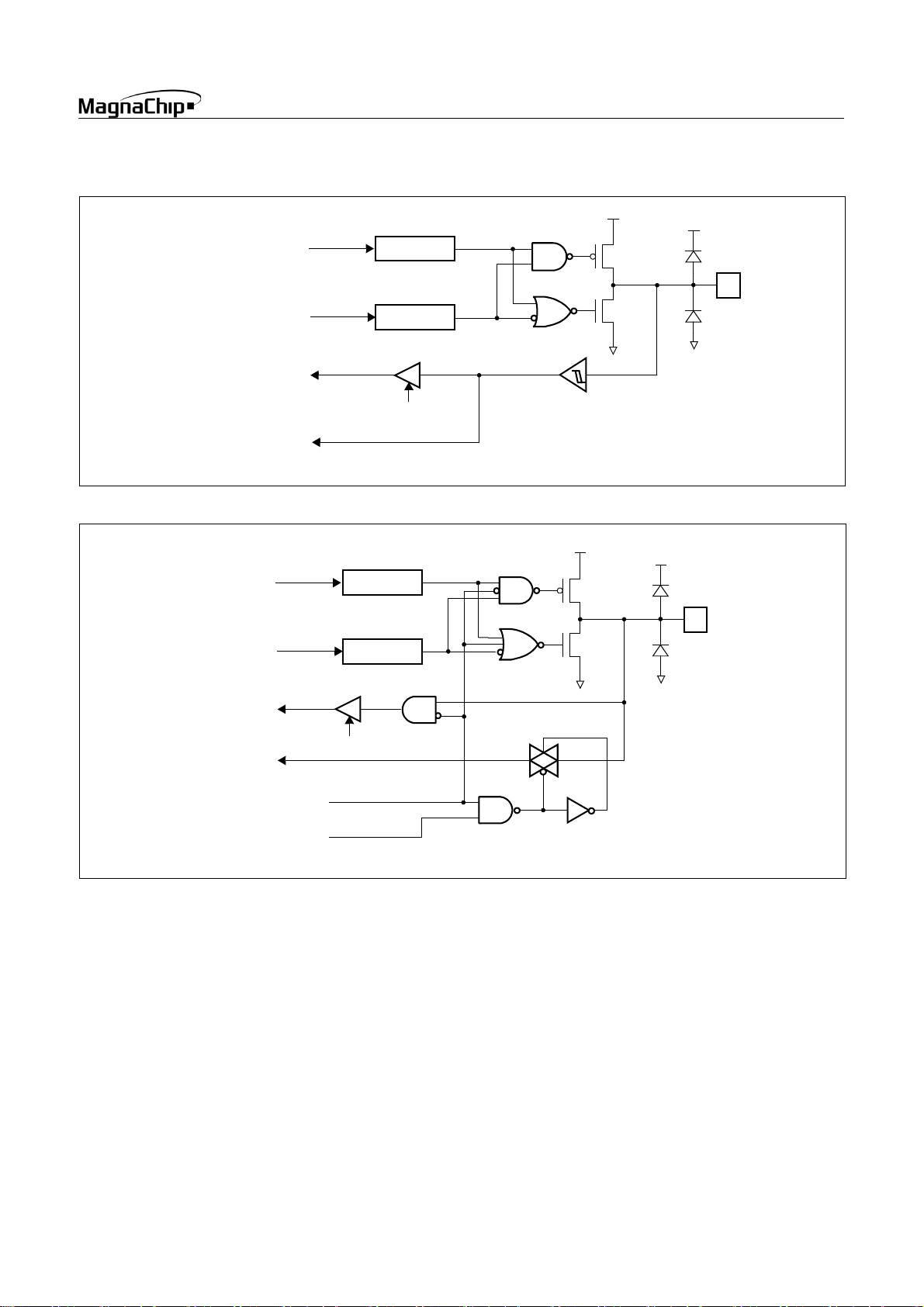
42 SDIP
MAX 0.190
1.470
1.450
HMS87C1X04B/08B/16B
unit: inch
MAX
MIN
TYP 0.600
0.550
0.530
MIN 0.015
44 MQFP
0.020
0.016
2
1
0
.
0
8
0
0
.
0
0.045
TYP 0.070
0.140
0.120
0 ~ 15°
0.035
13.45
12.95
10.10
09.90
unit: mm
MAX
MIN
13.45
12.95
10.10
09.90
0-7°
SEE DETAIL “A”
0.25
0.10
1.03
0.73
0.25
REF
2.35 max.
0.45
0.30
0.80 Typ.
1.60
REF
DETAIL “A”
SEP. 2004 Ver 1.03 9

HMS87C1X04B/08B/16B
5. PIN FUNCTION
VDD: Supply voltage.
V
: Circuit ground.
SS
RESET: Reset the MCU.
XIN: Input to the inverting oscillator amplifier and input to the in-
ternal main clock operating circuit.
X
: Output from the inverting oscillator amplifier.
OUT
RA0~RA7: RA is an 8-bit, CMOS, bidirectional I/O port. RA
pins can be used as outputs or inputs according to “1” or “0” written the their Port Direction Register(RAIO).
Port pin Alternate function
RA0
RA1
RA2
RA3
RA4
RA5
RA6
RA7
EC0 ( Event Counter Input Source )
AN1 ( Analog Input Port 1 )
AN2 ( Analog Input Port 2 )
AN3 ( Analog Input Port 3 )
AN4 ( Analog Input Port 4 )
AN5 ( Analog Input Port 5 )
AN6 ( Analog Input Port 6 )
AN7 ( Analog Input Port 7 )
Table 5-1 RA Port
In addition, RA serves the functions of the various special features in Table 5-1 .
RB0~RB7: RB is an 8-bit, CMOS, bidirectional I/O port. RB
pins can be used as outputs or inputs according to “1” or “0” written the their Port Direction Register (RBIO).
RB serves the functions of the various following special features
Table 5-2
in
Port pin Alternate function
RB0
AN0 ( Analog Input Port 0 )
AVref ( External Analog Reference Pin )
RB1
RB2
RB3
RB4
BUZ ( Buzzer Driving Output Port )
INT0 ( External Interrupt Input Port 0 )
INT1 ( External Interrupt Input Port 1 )
PWM0 (PWM0 Output)
COMP0 (Timer1 Compare Output)
RB5
PWM1 (PWM1 Output)
COMP1 (Timer3 Compare Output)
RB6
RB7
EC1 (Event Counter Input Source)
TMR2OV (Timer2 Overflow Output)
RC0~RC7: RC is an 8-bit, CMOS, bidirectional I/O port. RC
pins can be used as outputs or inputs according to “1” or “0” written the their Port Direction Register (RCIO).
RC serves the functions of the serial interface following special
features in Table 5-3 .
Port pin Alternate function
RC0
RC1
RC2
RC3
SRDYIN
(SPI Ready Input)
SRDYOUT (SPI Ready Output)
RC4
SCKI (SPI CLK Input)
SCKO (SPI CLK Output)
RC5
RC6
SIN (SPI Serial Data Input)
SOUT (SPI Serial Data Output)
RC7
Table 5-3 RC Port
RD0~RD7: RD is an 8-bit, CMOS, bidirectional I/O port. RC
pins can be used as outputs or inputs according to “1” or “0” written the their Port Direction Register (RDIO).
RD serves the functions of the external interrupt following special features in Table 5-4
Port pin Alternate function
RD0
RD1
INT2 (External Interrupt Input Port 2)
INT3 (External Interrupt Input Port 3)
RD2
RD3
RD4
RD5
RD6
RD7
Table 5-4 RD Port
RE0~RE6: RE is a 7-bit, CMOS, bidirectional I/O port. RC pins
can be used as outputs or inputs according to “1” or “0” written
the their Port Direction Register (REIO).
Table 5-2 RB Port
PIN NAME Pin No. In/Out Function
V
DD
V
SS
43
34
-
-
Supply voltage
Circuit ground
Table 5-5 Pin Description
10 SEP. 2004 Ver 1.03

HMS87C1X04B/08B/16B
PIN NAME Pin No. In/Out Function
RESET 33
X
X
IN
OUT
31
32
RA0 (EC0) 35
RA1 (AN1) 36 Analog Input Port 1
RA2 (AN2) 37 Analog Input Port 2
RA3 (AN3) 38 Analog Input Port 3
RA4 (AN4) 39 Analog Input Port 4
RA5 (AN5) 40 Analog Input Port 5
RA6 (AN6) 41 Analog Input Port 6
RA7 (AN7) 42 Analog Input Port 7
RB0 (AVref/AN0) 44
RB1 (BUZ) 1
RB2 (INT0) 2
RB3 (INT1) 3
RB4 (PWM0/COMP0) 4
RB5 (PWM1/COMP1) 5
RB6 (EC1) 6
RB7 (TMR2OV) 7
RC0 ~ RC2 15 ~ 17
RC3 (SRDYIN/SRDYOUT)18
RC4 (SCK) 19
RC5 (SIN) 20
RC6 (SOUT) 21
RC7 22
RD0 (INT2) 23
RD1 (INT3) 24
RD2 25
RD3 ~ RD7 26 ~ 30
RE0 ~ RE6 14 ~8
I
I
O
I/O (Input)
I/O (Input/Input)
I/O (Output)
I/O (Input)
I/O (Input)
I/O (Output/Output)
I/O (Output/Output)
I/O (Input)
I/O (Output)
I/O
I/O (Input/Output)
I/O (Input/Output)
I/O (Input)
I/O (Output)
I/O
I/O (Input)
I/O (Input)
I/O
Reset signal input
Oscillation Input
Oscillation Output
Normal I/O Ports
External Event Counter input 0
Analog Reference / Analog Input Port 0
Buzzer Driving Output
External Interrupt Input 0
External Interrupt Input 1
PWM0 Output or Timer1 Compare Output
PWM1 Output or Timer3 Compare Output
External Event Counter input 1
Timer2 Overflow Output
SPI READY Input/Output
SPI CLK Input/Output
SPI DATA Input
SPI DATA Output
External Interrupt Input 2
External Interrupt Input 3
Table 5-5 Pin Description
SEP. 2004 Ver 1.03 11

HMS87C1X04B/08B/16B
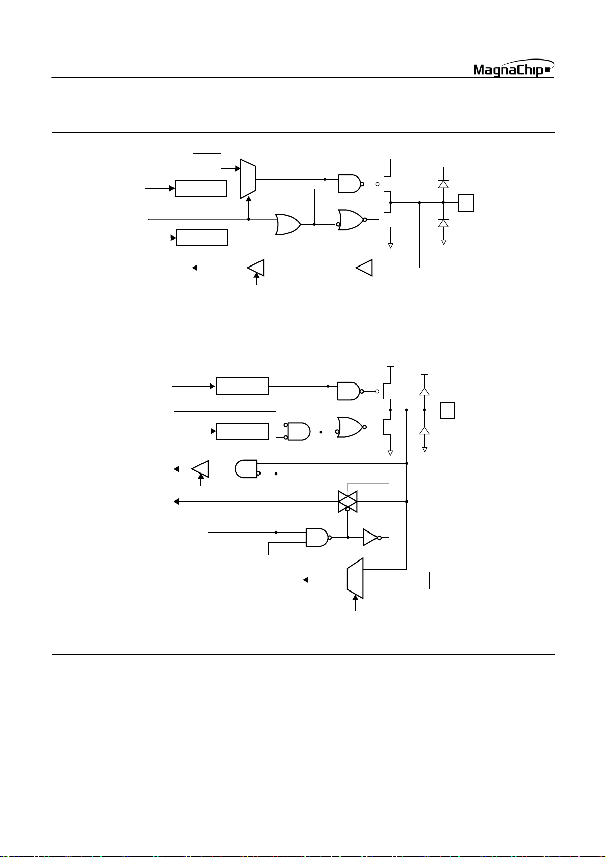
6. PORT STRUCTURES
• RESET
Internal RESET
• Xin, Xout (Crystal or Ceramic Resonator)
V
SS
STOP
To System CLK
• Xin, Xout (RC or R oscillation)
Internal Cap = 6.0pF
RC
OSC
V
V
DD
V
DD
DD
V
DD
Xout
V
SS
Xin
V
DD
V
DD
Xout
V
SS
STOP
To System CLK
Xin
12 SEP. 2004 Ver 1.03
• RA0/EC0, RB6/EC1
• RA1/AN1 ~ RA7/AN7
Data Bus
Data Bus
Data Bus
Data Bus
EC0, EC1
Direction Reg.
Data Reg.
Data Reg.
Read
HMS87C1X04B/08B/16B
V
DD
Direction Reg.
Data Bus
Data Bus
Read
To A/D Converter
Analog Input Mode
(ANSEL7 ~ 1)
Analog CH. Selection
(ADCM.4 ~ 2)
• RB1/BUZ, RB4/PWM0/COMP0, RB5/PWM1/
V
SS
SEP. 2004 Ver 1.03 13
HMS87C1X04B/08B/16B
COMP1, RB7/TMR2OV, RC6/SOUT
PWM/COMP
BUZ,TMR2OV,SOUT
Data Reg.
Data Bus
V
1
0
DD
Function
Select
Data Bus
• RB0 / AN0 / AVref
Data Bus
AVREFS
Data Bus
Data Bus
To A/D Converter
Data Bus
Direction Reg.
Read
Read
Data Reg.
Direction Reg.
V
SS
V
DD
V
SS
Analog Input Mode
(ANSEL0)
Analog CH0 Selection
(ADCM.4 ~ 2)
To Vref of A/D
1
0
AVREFS
Internal V
DD
14 SEP. 2004 Ver 1.03

• RB2/INT0, RB3/INT1, RD0/INT2, RD1/INT3
Pull-up
Select
HMS87C1X04B/08B/16B
Weak Pull-up
• RC5/SIN
Data Bus
Function
Select
Data Bus
Data Bus
INT0, INT1
INT2, INT3
Data Bus
Function
Select
Data Bus
Data Reg.
Direction Reg.
Data Reg.
Direction Reg.
Read
Schmitt Trigger
V
DD
V
SS
V
DD
Data Bus
SIN
Read
Schmitt Trigger
V
SS
SEP. 2004 Ver 1.03 15
HMS87C1X04B/08B/16B
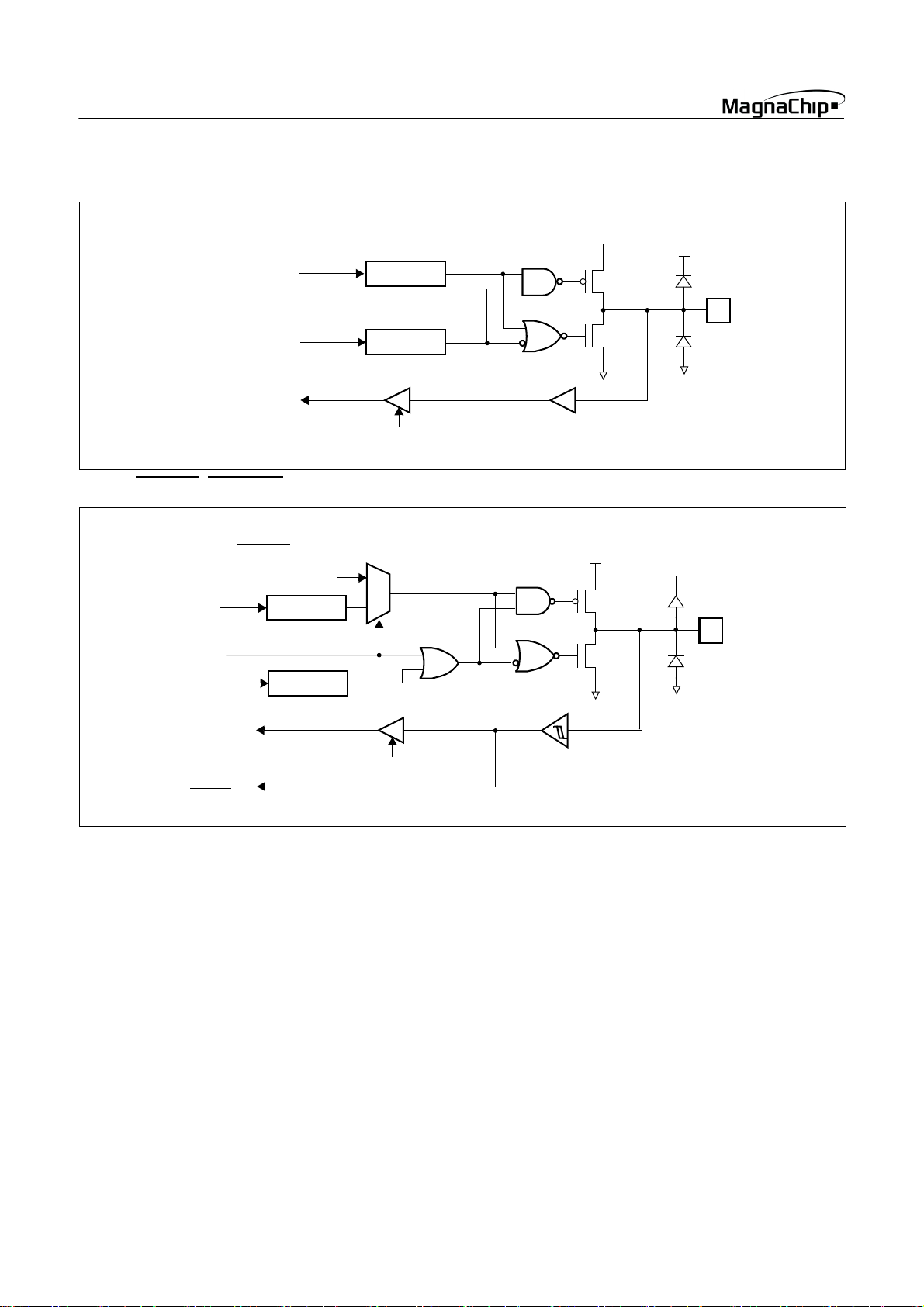
• RC0~2, RC7, RD2~7, RE0~6
Data Bus
Data Bus
Data Bus
Data Reg.
Direction Reg.
Read
V
DD
V
SS
• RC3 / SRDYIN
Data Bus
Function
Select
Data Bus
Data Bus
/ SRDYOUT, RC4 / SCKIN / SCK- OUT
SRDYOUT
SCKOUT
Data Reg.
Direction Reg.
SCKIN
SRDYIN
1
0
Read
Schmitt Trigger
V
DD
V
SS
16 SEP. 2004 Ver 1.03

7. ELECTRICAL CHARACTERISTICS
7.1 Absolute Maximum Ratings
Supply voltage......................................................-0.3 to +6.0 V
Storage Temperature .......................................... -40 to +125 °C
Voltage on any pin with respect to Ground (V
.......................................................................... -0.3 to VDD+0.3
Maximum current out of V
pin.................................. 200 mA
SS
Maximum current into VDD pin.................................... 150 mA
Maximum current sunk by (I
Maximum output current sourced by (I
......................................................................................... 15 mA
Maximum current (ΣI
OL
per I/O Pin) .................. 25 mA
OL
OH
) .............................................. 150 mA
7.2 Recommended Operating Conditions
)
SS
per I/O Pin)
HMS87C1X04B/08B/16B
Maximum current (ΣI
Note: Stresses above those listed under “Absolute Maximum Ratings” may cause permanent damage to the device. This is a stress rating only and functional operation of
the device at any other conditions above those indicated in
the operational sections of this specification is not implied.
Exposure to absolute maximum rating conditions for extended periods may affect device reliability.
).............................................. 100 mA
OH
Parameter Symbol Condition
T
V
f
XIN
OPR
DD
Supply Voltage
Operating Frequency
Operating Temperature
7.3 A/D Converter Characteristics
(TA=25°C, VSS=0V, VDD=5.12V @f
Parameter Symbol Condition
Analog Input Voltage Range
Analog Power Supply Input Voltage Range
Overall Accuracy
Non-Linearity Error
Differential Non-Linearity Error
Zero Offset Error
Full Scale Error
Gain Error
Conversion Time
AV
Input Current
REF
=8MHz, VDD=3.072V @f
XIN
f
=8MHz
XIN
f
=4.2MHz
XIN
VDD=4.5~5.5V
VDD=2.3~5.5V
XIN
V
AIN
V
REF
N
ACC
N
NLE
N
DNLE
N
ZOE
N
FSE
N
NLE
T
CONV
I
REF
Specifications
Unit
Min. Max.
4.5 5.5 V
2.3 5.5 V
18MHz
14.2MHz
-40 85 °C
=4MHz)
Specifications
Unit
Min. Typ. Max.
AVREFS=0
AVREFS=1
VDD=5V
V
=3V
DD
V
SS
V
SS
-
-
3-
2.4 -
V
DD
V
REF
V
DD
V
DD
- ±0.7 ±1.5 LSB
- ±0.8 ±1.5 LSB
- ±1.0 ±1.5 LSB
- ±1.0 ±1.5 LSB
- ±0.25 ±0.5 LSB
- ±1.0 ±1.5 LSB
f
f
XIN
XIN
=8MHz
=4MHz
--10
--20
AVREFS=1 - 0.5 1.0 mA
V
V
V
µS
SEP. 2004 Ver 1.03 17

HMS87C1X04B/08B/16B
7.4 DC Electrical Characteristics
(TA=-40~85°C, VDD=2.3~5.5V, VSS=0V),
Parameter Symbol Pin Condition
Min. Typ. Max.
V
Input High Voltage
V
V
V
Input Low Voltage
V
V
Output High Voltage
Output Low Voltage
V
V
Input Pull-up Current
Input High
Leakage Current
Input Low
Leakage Current
Hysteresis
PFD Voltage
Internal RC WDT
Period
Operating Current
Wake-up Timer
Mode Current
2
I
I
I
I
| V
V
T
RCWDT
I
I
WKUP
RCWDT Mode
Current at STOP
I
RCWDT
Mode
Stop Mode Current
INT Input Noise
Cancel Time
External RC
Oscillator Frequency
1. Hysteresis Input: RA0, RB2, RB3, RB6, RC3, RC4, RC5, RD0, RD1
2. This parameter is measured in internal EPROM operation at the all I/O port defined input mode.
I
STOP
T
INT_NC
f
RC-OSC
f
R-OSC
XIN, RESET
IH1
Hysteresis Input
IH2
Normal Input
IH3
XIN, RESET 0-
IL1
Hysteresis Input
IL2
Normal Input 0 -
IL3
All Output Port VDD=5V, IOH=-5mA
OH
All Output Port VDD=5V, IOL=10mA
OL
I
RB2, RB3, RD0, RD1 VDD=5V -150 - -70 µA
P
All Pins (except XIN)VDD=5V - - 5 µA
IH1
X
IH2
IL1
IL2
T
PFD
DD
IN
All Pins (except XIN)VDD=5V -5 - - µA
X
IN
|
Hysteresis Input
V
DD
X
OUT
V
DD
V
DD
1
1
VDD=5V - - 15 µA
VDD=5V -15 - - µA
1
VDD=5V 0.5 - - V
VDD=5.5V 30 - 100
=3.0V 60 - 180
V
DD
VDD=5.5V, f
=3.0V, f
V
DD
VDD=5.5V, f
V
=3.0V, f
DD
=8MHz - 4 6.5
XIN
=4MHz - 2 3
XIN
=8MHz - 1 2
XIN
=4MHz - 0.3 1
XIN
VDD=5.5V - 30 70
V
DD
V
DD
RB2, RB3, RD0, RD1
f
XOUT
f
XOUT
= f
= f
RC-OSC
R-OSC
/ 4
/ 4
V
=3.0V - 5 50
DD
VDD=5.5V, f
=3.0V, f
V
DD
=8MHz - 0.5 3
XIN
=4MHz - 0.2 1
XIN
VDD=5V 0.2 - 0.5 µS
V
=5.5V
DD
R=30kΩ, C=10pF
V
=5.5V
DD
R=30kΩ
0.8 V
0.8 V
0.7 V
V
Specifications
Unit
DD
DD
DD
-
-
-
0-
DD
-1
-
--V
-1V
V
V
V
0.2 V
0.2 V
0.3 V
DD
DD
DD
DD
DD
DD
V
V
2.1 - 3.1 V
µS
mA
mA
µA
µA
0.7 - 1.5 MHz
2-4MHz
18 SEP. 2004 Ver 1.03
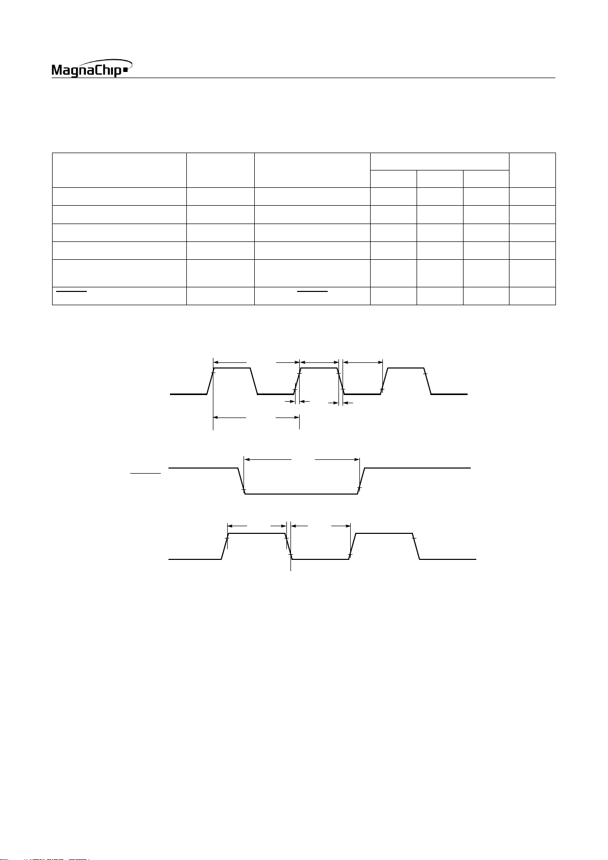
7.5 AC Characteristics
(TA=-40~+85°C, VDD=5V±10%, VSS=0V)
HMS87C1X04B/08B/16B
Parameter Symbol Pins
Operating Frequency
External Clock Pulse Width
External Clock Transition Time
Oscillation Stabilizing Time
External Input Pulse Width
RESET Input Width
X
IN
f
CP
t
CPW
t
RCP,tFCP
t
ST
t
EPW
t
RST
X
IN
X
IN
X
IN
XIN, X
OUT
INT0, INT1, INT2, INT3
EC0, EC1
RESET 8- -
t
t
1/f
SYS
CP
t
RCP
CPW
t
FCP
t
Specifications
Min. Typ. Max.
1-8MHz
50 - - nS
--20nS
--20mS
2--
CPW
V
0.5V
DD
-0.5V
Unit
t
SYS
t
SYS
RESET
INT0, INT1
INT3
INT2,
EC0,
EC1
t
RST
t
EPW
t
EPW
Figure 7-1 Timing Chart
0.2V
0.2V
DD
DD
0.8V
DD
SEP. 2004 Ver 1.03 19
HMS87C1X04B/08B/16B
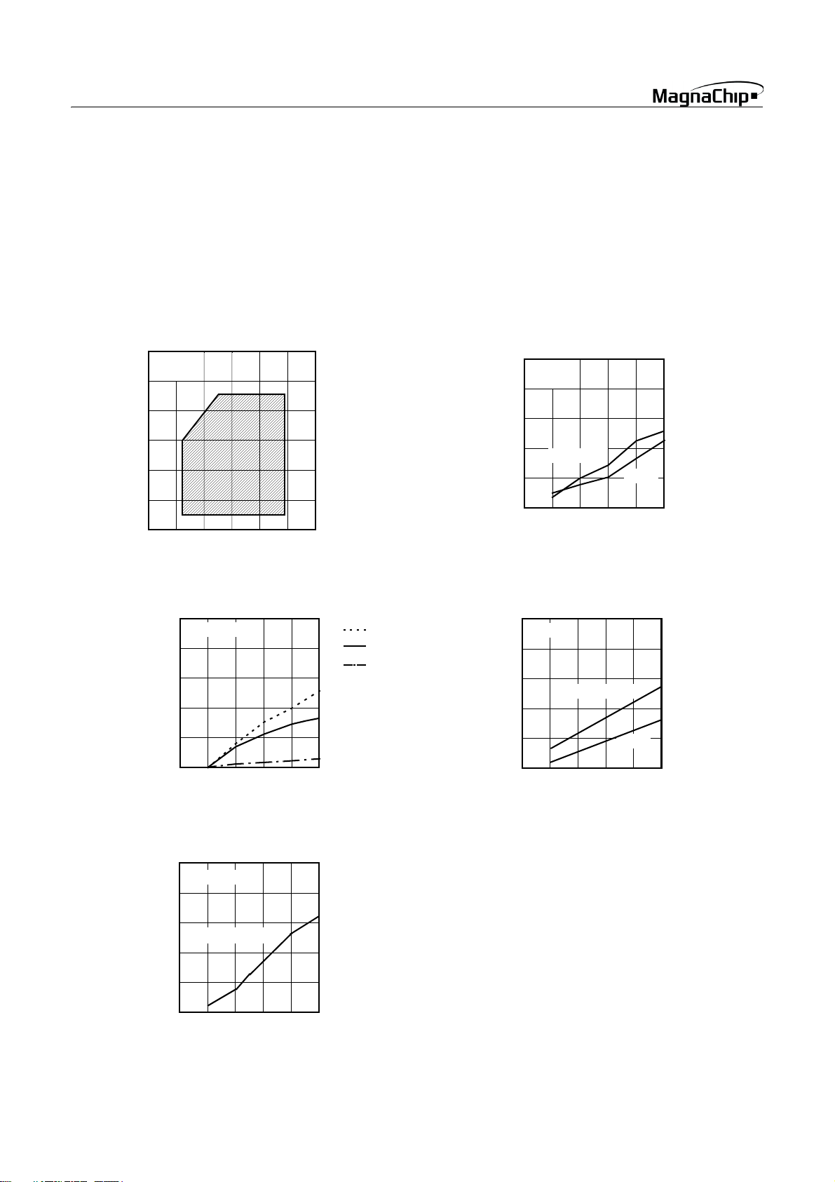
7.6 Typical Characteristics
These graphs and tables provided in this section are for design
guidance only and are not tested or guaranteed.
In some graphs or tables the data presented are outside specified operating range (e.g. outside specified
range). This is for information only and devices
V
DD
are guaranteed to operate properly only within the
specified range.
The data presented in this section is a statistical summary of data
collected on units from different lots over a period of time. “Typical” represents the mean of the distribution while “max” or
“min” represents (mean + 3σ) and (mean − 3σ) respectively
where σ is standard deviation
Operating Area
f
XIN
(MHz)
Ta= 25°C
10
8
6
4
2
0
23
I
DD
(µA)
0.8
0.6
0.4
45
STOP Mode
I
STOP−VDD
f
= 8MHz
XIN
Normal Operation
IDD−V
Ta=25°C
f
XIN
23
DD
= 8MHz
4MHz
45
V
DD
(V)
6
I
DD
(mA)
8
6
4
2
0
V
DD
(V)
6
Wake-up Timer Mode
I
WKUP−VDD
I
-25°C
25°C
85°C
DD
(mA)
2.0
1.5
1.0
Ta=25°C
f
XIN
= 8MHz
0.2
0
23
45
V
DD
(V)
6
0.5
0
23
4MHz
45
V
DD
(V)
6
RC-WDT in Stop Mode
I
RCWDT−VDD
I
DD
(µA)
Ta=25°C
20
15
T
= 80uS
5
RCWDT
23
45
V
DD
(V)
6
10
0
20 SEP. 2004 Ver 1.03

HMS87C1X04B/08B/16B
V
(V)
IH1
4
3
2
IOL−VOL, VDD=5V
I
OL
(mA)
40
30
20
10
0
12 345
VDD−V
f
=4MHz
XIN
Ta=25°C
IH1
XIN, RESET
IOH−VOH, VDD=5V
I
OH
-25°C
25°C
85°C
V
OL
(V)
VDD−V
IH2
V
IH2
f
=4kHz
XIN
(V)
Ta=25°C
4
3
2
(mA)
-20
-15
-10
-5
0
23 456
Hysteresis input
V
(V)
IH3
4
3
2
VDD−V
f
=4kHz
XIN
Ta=25°C
IH3
V
OH
(V)
-25°C
25°C
85°C
Normal input
V
IL1
(V)
1
0
1
VDD−V
f
XIN
Ta=25°C
4
3
2
1
0
1
23
IL1
XIN, RESET
=4MHz
23
45
45
1
V
(V)
0
IL2
4
3
2
1
0
23
VDD−V
f
=4kHz
XIN
Ta=25°C
23
45
IL2
Hysteresis input
45
V
DD
(V)
6
V
DD
(V)
6
V
DD
(V)
6
V
DD
(V)
6
V
(V)
1
0
IL3
4
3
2
1
0
23
VDD−V
f
=4kHz
XIN
Ta=25°C
23
IL3
Normal input
45
45
V
DD
(V)
6
V
DD
(V)
6
SEP. 2004 Ver 1.03 21

HMS87C1X04B/08B/16B
F
OSC
(MHz)
F
OSC
(MHz)
Typical RC Oscillator
Frequency vs V
6
No Cap
Ta = 25°C
5
4
R = 10K
3
2
1
0
2.5 3.0 3.5 4.0 4.5
Typical RC Oscillator
Frequency vs V
6
C
= 20p
EXT
Ta = 25°C
5
DD
R = 20K
R = 30K
DD
R = 51K
5.0 5.5
Typical RC Oscillator
Frequency vs V
F
OSC
6
(MHz)
V
DD
(V)
C
= 10p
EXT
Ta = 25°C
5
4
3
2
1
0
2.5 3.0 3.5 4.0 4.5
R = 10K
DD
R = 20K
R = 30K
R = 51K
5.0 5.5
V
DD
(V)
Typical RC Oscillator
F
OSC
(MHz)
6
5
Frequency vs V
C
= 30p
EXT
Ta = 25°C
DD
4
3
R = 10K
2
R = 20K
1
0
2.5 3.0 3.5 4.0 4.5
R = 30K
R = 51K
5.0
5.5
V
DD
(V)
Note: The external RC oscillation frequencies shown in
above are provided for design guidance only and not tested
or guaranteed. The user needs to take into account that the
external RC oscillation frequencies generated by the same
circuit design may be not the same. Because there are variations in the resistance and capacitance due to the tolerance of external R and C components. The parasitic
capacitance difference due to the different wiring length
and layout may change the external RC oscillation frequencies.
4
3
R = 10K
2
1
0
2.5 3.0 3.5 4.0 4.5
R = 20K
R = 30K
R = 51K
5.0
5.5
V
DD
(V)
Note: The external RC oscillation frequencies of the
HMS87C1X04B/08B/16B may be different from that of the
HMS81C1X04B/08B/16B. The user should modify the value of R and C components to get the proper frequency in
exchanging OTP device to mask device.
22 SEP. 2004 Ver 1.03
8. MEMORY ORGANIZATION
HMS87C1X04B/08B/16B
The HMS87C1X04B/08B/16B has separate address spaces for
Program memory and Data Memory. The Program memory can
only be read, not written to. It can be up to 4K /8K /16K bytes of
8.1 Registers
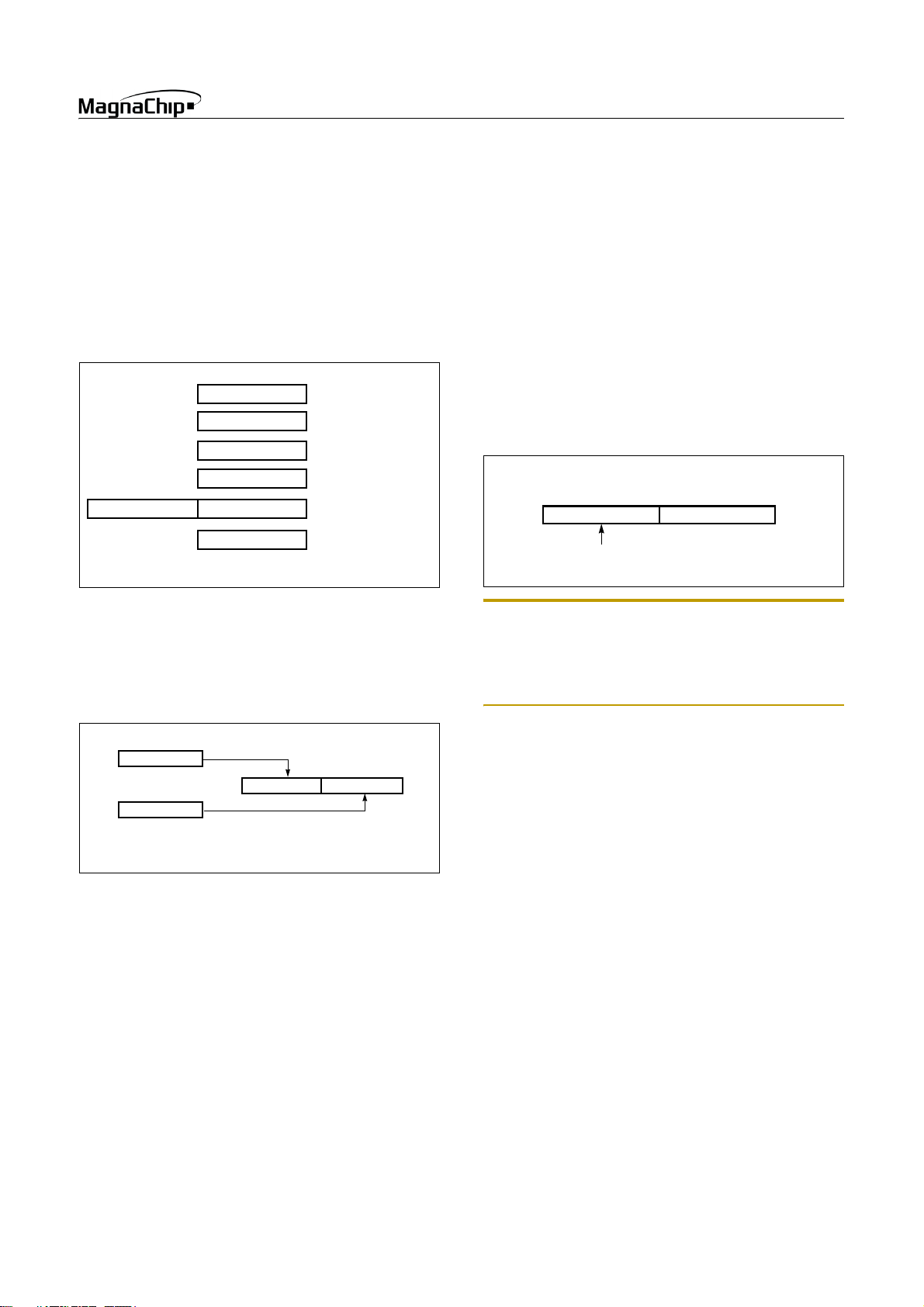
This device has six registers that are the Program Counter (PC),
a Accumulator (A), two index registers (X, Y), the Stack Pointer
(SP), and the Program Status Word (PSW). The Program Counter
consists of 16-bit register.
A
X
Y
SP
PCLPCH
PSW
Figure 8-1 Configuration of Registers
Accumulator: The Accumulator is the 8-bit general purpose register, used for data operation such as transfer, temporary saving,
and conditional judgement, etc.
The Accumulator can be used as a 16-bit register with Y Register
as shown below.
Y
A
Two 8-bit Registers can be used as a “YA” 16-bit Register
Figure 8-2 Configuration of YA 16-bit Register
X, Y Registers: In the addressing mode which uses these index
registers, the register contents are added to the specified address,
which becomes the actual address. These modes are extremely effective for referencing subroutine tables and memory tables. The
index registers also have increment, decrement, comparison and
data transfer functions, and they can be used as simple accumulators.
Stack Pointer: The Stack Pointer is an 8-bit register used for occurrence interrupts and calling out subroutines. Stack Pointer
identifies the location in the stack to be accessed (save or restore).
ACCUMULATOR
X REGISTER
Y REGISTER
STACK POINTER
PROGRAM COUNTER
PROGRAM STATUS
WORD
Y A
Program memory. The Data memory can be read and written to
up to 448 bytes including the stack area.
Generally, SP is automatically updated when a subroutine call is
executed or an interrupt is accepted. However, if it is used in excess of the stack area permitted by the data memory allocating
configuration, the user-processed data may be lost.
The stack can be located at any position within 00
to BFH of the
H
internal data memory. The SP is not initialized by hardware, requiring to write the initial value (the location with which the use
of the stack starts) by using the initialization routine. Normally,
the initial value of “BF
15 087
” is used.
H
Stack Address (00
00
Hardware fixed
~ BFH)
H
SP
Note: The Stack Pointer must be initialized by software because its value is undefined after RESET.
Example: To initialize the SP
LDX #0BFH
TXSP ; SP ← BFH
Program Counter: The Program Counter is a 16-bit wide which
consists of two 8-bit registers, PCH and PCL. This counter indicates the address of the next instruction to be executed. In reset
state, the program counter has reset routine address (PC
PC
:0FEH).
L
:0FFH,
H
Program Status Word: The Program Status Word (PSW) contains several bits that reflect the current state of the CPU. The
PSW is described in Figure 8-3 . It contains the Negative flag, the
Overflow flag, Direct page select flag, the Break flag, the Half
Carry (for BCD operation), the Interrupt enable flag, the Zero
flag, and the Carry flag.
[Carry flag C]
This flag stores any carry or borrow from the ALU of CPU after
an arithmetic operation and is also changed by the Shift Instruction or Rotate Instruction.
[Zero flag Z]
This flag is set when the result of an arithmetic operation or data
transfer is “0” and is cleared by any other result.
SEP. 2004 Ver 1.03 23

HMS87C1X04B/08B/16B
NEGATIVE FLAG
OVERFLOW FLAG
PSW
MSB LSB
N
V G B H I Z C
RESET VALUE: 00
CARRY FLAG RECEIVES
CARRY OUT
ZERO FLAG
H
DIRECT PAGE SELECT FLAG
BRK FLAG
Figure 8-3 PSW (Program Status Word) Register
[Interrupt disable flag I]
This flag enables/disables all interrupts except interrupt caused
by Reset or software BRK instruction. All interrupts are disabled
when cleared to “0”. This flag immediately becomes “0” when an
interrupt is served. It is set by the EI instruction and cleared by
the DI instruction.
[Half carry flag H]
After operation, this is set when there is a carry from bit 3 of ALU
or there is no borrow from bit 4 of ALU. This bit can not be set
or cleared except CLRV instruction with Overflow flag (V).
[Break flag B]
This flag is set by software BRK instruction to distinguish BRK
from TCALL instruction with the same vector address.
[Direct page select flag G]
INTERRUPT ENABLE FLAG
HALF CARRY FLAG RECEIVES
CARRY OUT FROM BIT 1 OF
ADDITION OPERLANDS
This flag assigned direct page for direct addressing mode. In the
direct addressing mode, addressing area is within zero page 00
to FFH when this flag is “0”. If it is set to “1”, addressing area is
100H to 1FFH.
It is set by SETG instruction, and cleared by CLRG instruction.
[Overflow flag V]
This flag is set to “1” when an overflow occurs as the result of an
arithmetic operation involving signs. An overflow occurs when
the result of an addition or subtraction exceeds +127(7F
) or -
H
128(80H). The CLRV instruction clears the overflow flag. There
is no set instruction. When the BIT instruction is executed, bit 6
of memory is copied to this flag.
[Negative flag N]
This flag is set to match the sign bit (bit 7) status of the result of
a data or arithmetic operation. When the BIT instruction is executed, bit 7 of memory is copied to this flag.
H
24 SEP. 2004 Ver 1.03
8.2 Program Memory
A 16-bit program counter is capable of addressing up to 64K
bytes, but these devices have 4K/8K/16K bytes program memory
space only physically implemented. Accessing a location above
will cause a wrap-around to 0000H.
FFFF
H
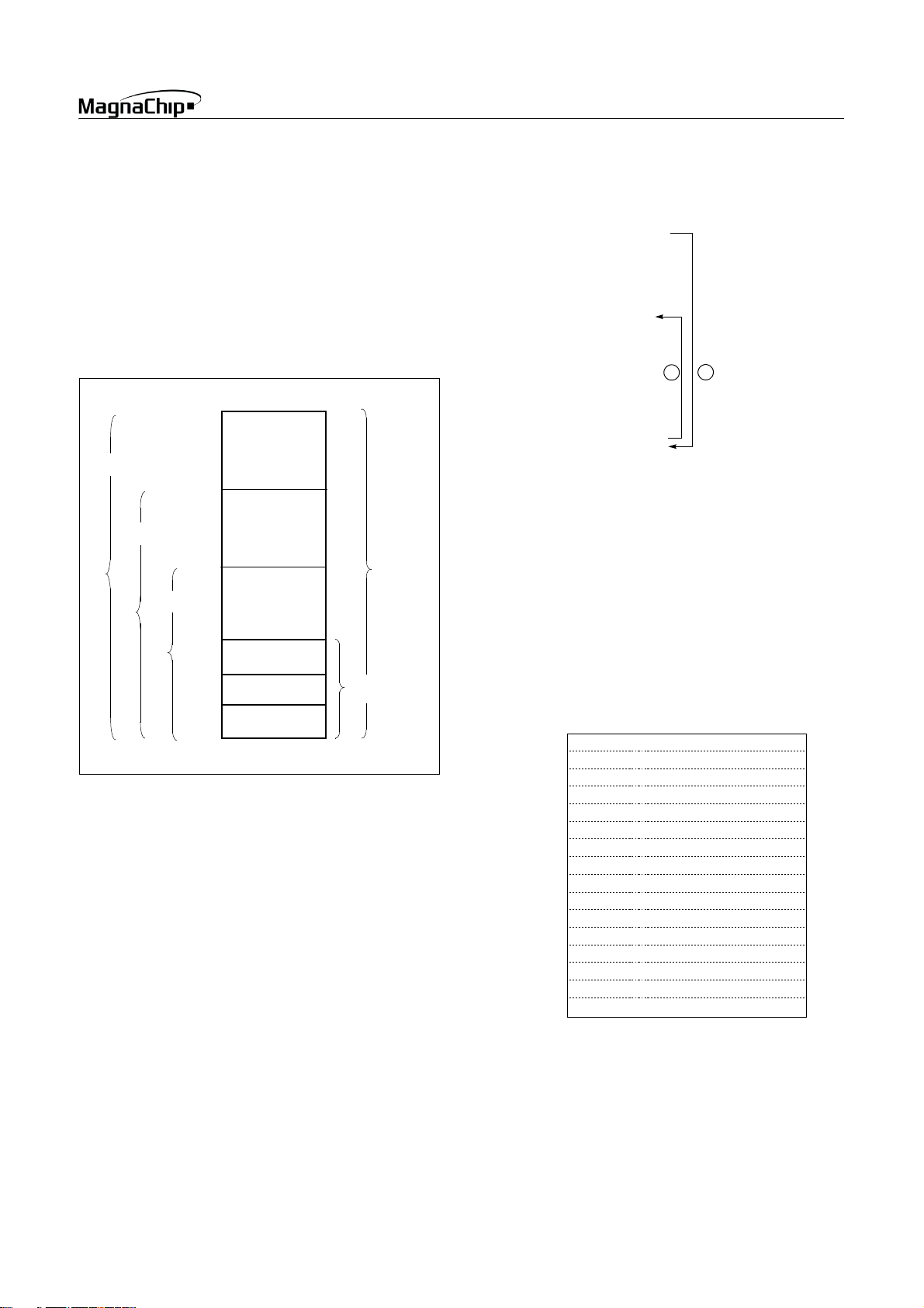
Figure 8-4 , shows a map of Program Memory. After reset, the
CPU begins execution from reset vector which is stored in address FFFEH and FFFFH as shown in Figure 8-5 .
As shown in Figure 8-4 , each area is assigned a fixed location in
Program Memory. Program Memory area contains the user program.
C000H
HMS87C1X16B
E000H
Example: Usage of TCALL
LDA #5
TCALL 0FH ;
:;
:;
;
;TABLE CALL ROUTINE
;
FUNC_A: LDA LRG0
RET
;
FUNC_B: LDA LRG1
RET
;
;TABLE CALL ADD. AREA
;
ORG 0FFC0H ;
DW FUNC_A
DW FUNC_B
HMS87C1X04B/08B/16B
1BYTE INSTRUCTION
INSTEAD OF 3 BYTES
NORMAL CALL
1
2
TCALL ADDRESS AREA
HMS87C1X08B
F000H
HMS87C1X04B
FEFFH
FF00H
FFC0H
FFDFH
FFE0H
FFFFH
TCALL
AREA
INTERRUPT
VECTOR AREA
PROGRAM
MEMORY
PCALL
AREA
Figure 8-4 Program Memory Map
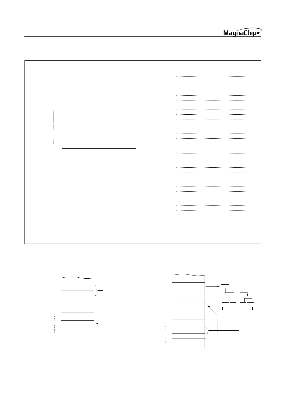
Page Call (PCALL) area contains subroutine program to reduce
program byte length by using 2 bytes PCALL instead of 3 bytes
CALL instruction. If it is frequently called, it is more useful to
save program byte length.
Table Call (TCALL) causes the CPU to jump to each TCALL address, where it commences the execution of the service routine.
The Table Call service area spaces 2-byte for every TCALL:
0FFC0
for TCALL15, 0FFC2H for TCALL14, etc., as shown in
H
Figure 8-6 .
The interrupt causes the CPU to jump to specific location, where
it commences the execution of the service routine. The External
interrupt 0, for example, is assigned to location 0FFFA
. The in-
H
terrupt service locations spaces 2-byte interval: 0FFF8H and
0FFF9H for External Interrupt 1, 0FFFAH and 0FFFBH for External Interrupt 0, etc.
As for the area from 0FF00H to 0FFFFH, if any area of them is not
going to be used, its service location is available as general purpose Program Memory.
Address Vector Area Memory
0FFE0
H
E2
E4
Serial Peripheral Interface Interrupt Vector Area
E6
E8
EA
EC
EE
F0
F2
F4
F6
F8
FA
FC
FE
Basic Interval Interrupt Vector Area
Watchdog Timer Interrupt Vector Area
A/D Converter Interrupt Vector Area
Timer/Counter 3 Interrupt Vector Area
Timer/Counter 2 Interrupt Vector Area
External Interrupt 3 Vector Area
External Interrupt 2 Vector Area
Timer/Counter 1 Interrupt Vector Area
Timer/Counter 0 Interrupt Vector Area
External Interrupt 1 Vector Area
External Interrupt 0 Vector Area
-
-
-
RESET Vector Area
NOTE:
“-” means reserved area.
Figure 8-5 Interrupt Vector Area
SEP. 2004 Ver 1.03 25
HMS87C1X04B/08B/16B
Address PCALL Area Memory
0FF00
H
0FFFF
H
PCALL Area
(256 Bytes)
Address Program Memory
0FFC0
H
C1
C2
C3
C4
C5
C6
C7
C8
C9
CA
CB
CC
CD
CE
CF
D0
D1
D2
D3
D4
D5
D6
D7
D8
D9
DA
DB
DC
DD
DE
DF
NOTE:
* means that the BRK software interrupt is using
same address with TCALL0.
TCALL 15
TCALL 14
TCALL 13
TCALL 12
TCALL 11
TCALL 10
TCALL 9
TCALL 8
TCALL 7
TCALL 6
TCALL 5
TCALL 4
TCALL 3
TCALL 2
TCALL 1
TCALL 0 / BRK *
Figure 8-6 PCALL and TCALL Memory Area
PCALL→ rel
4F35 PCALL 35H
~
~
0FF00H
0FF35H
0FFFFH
4F
35
NEXT
~
~
TCALL→ n
4A TCALL 4
4A
~
~
0F125H
0FF00H
0FFD6H
0FFD7H
0FFFFH
NEXT
25
F1
01001010
~
~
PC:
11111111
FHFHDH6
3
Reverse
1
11010110
2
H
26 SEP. 2004 Ver 1.03
 Loading...