

Page 1
Ⅰ
. SCOPE
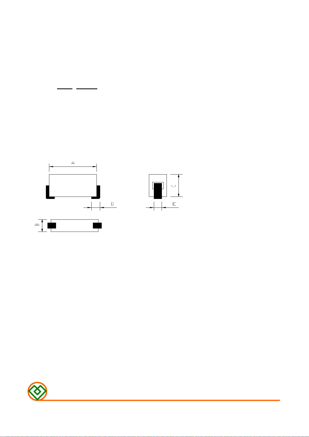
(1) SHAPES AND DIMENSIONS
(2) ELECTRICAL SPECIFICATIONS
(3) CHARACTERISTICS
:
This specification applies to the Pb Free Ferrite Chip Beads
for SMB-853025
PRODUCT INDENTIFICATION
SMB- 853025
① ②
① Product Code
② Dimensions Code
A: 8.5±0.3 mm
B: 3.1±0.15 mm
SEE TABLE 1
TEST INSTRUMENTS
Z : HP 4291B IMPEDANCE ANALYER (or equivalent)
RDC : CHROMA MODEL 16502 MILLIOHMMETER (or equivalent)
(3)-1 Temperature rise ...................... +40℃ Max.
C: 2.54±0.15 mm
D: 1.5 Typ. mm
E: 1.35 Typ. mm
(3)-2 Ambient temperature ................ +60℃ Max.
(3)-3 Operate temperature range ...... -40℃~+85℃
(Including self temp. rise)
(3)-4 Storage temperature range ...... -40℃~+105℃
MAG.LAYERS
SMB-853025 Page 1/7
Page 2

TABLE 1
MAGLAYERS PT/NO.
IMPEDANCE (Ω)
At 25MHz/0.5V (A)Max.
At 100MHz/0.5V
DCR(mΩ)
Max.
IDC
60±25% 90±25%SMB-853025
0.9 10.0
MAG.LAYERS
SMB-853025 Page-2/7
Page 3
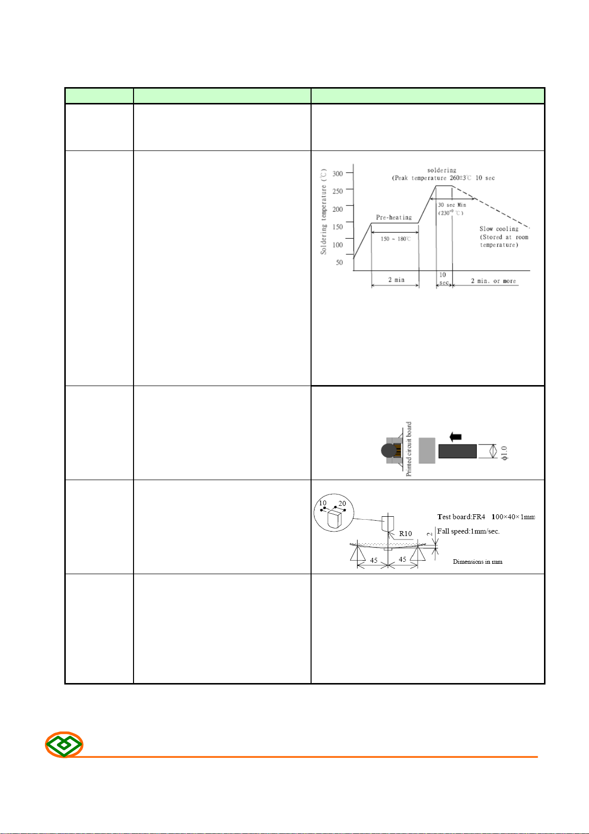
(4) RELIABILITY TEST METHOD
MECHANICAL
TEST ITEM SPECIFICATIONS TEST CONDITIONS
Solder The product shall be connected to the test Apply cream solder to the printed circuit board .
ability circuit board by the fillet (the height Refer to clause 8 for Reflow profile.
is 0.2mm).
Resistance to There shall be no damage or problems. Temperature profile of reflow soldering
Soldering
heat (reflow
soldering)
The specimen shall be passed through the reflow
oven with the condition shown in the above profile for 1 time.
The specimen shall be stored at standard atmospheric conditions for 1 hour, after which the measu-
rement shall be made.
Terminal The terminal electrode and the ferrite must Solder a chip to test substrate , and then
strength not damaged. laterally apply a load 9.8N in the arrow direction.
Strength on The terminal electrode and the ferrite must Solder a chip to test substrate and then apply a load.
PC board not damaged.
bending
High
temperature
resistance
Impedance:Within±20% of the initial value. After the samples shall be soldered onto the test
Insulation resistance and DC resistance on circuit board,the test shall be done.
the specification(refer to clause 2-1) Measurement : After placing for 24 hours min.
shall be met.
The terminal electrode and the ferrite must Applied voltage : Rated voltage
not damaged. Applied current : Rated current
Temperature : +85±2℃
Testing time : 500±12 hours
MAG.LAYERS
SMB-853025
Page-3/7
Page 4
TEST ITEM SPECIFICATIONS TEST CONDITIONS
Humidity Impedance:Within±20% of the initial value. After the samples shall be soldered onto the test
resistance Insulation resistance and DC resistance on circuit board,the test shall be done.
the specification(refer to clause 2-1) Measurement : After placing for 24 hours min.
shall be met.
The terminal electrode and the ferrite must Applied voltage : Rated voltage
not damaged. Applied current : Rated current
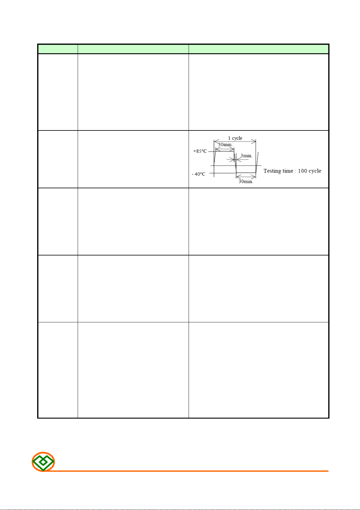
Thermal shock Impedance:Within±20% of the initial value.
Insulation resistance and DC resistance on
the specification(refer to clause 2-1)
shall be met.
The terminal electrode and the ferrite must
not damaged.
Low
temperature
storage
Impedance:Within±20% of the initial value. After the samples shall be soldered onto the test
Insulation resistance and DC resistance on circuit board,the test shall be done.
the specification(refer to clause 2-1) Measurement : After placing for 24 hours min.
shall be met.
The terminal electrode and the ferrite must Testing time : 500±12 hours
not damaged.
Temperature : +60±2℃ , Humidity : 90 to 95 %RH
Testing time : 500±12 hours
Temperature : -40±2℃
Vibration Impedance:Within±20% of the initial value. After the samples shall be soldered onto the test
Insulation resistance and DC resistance on circuit board,the test shall be done.
the specification(refer to clause 2-1) Frequency : 10 to 55 Hz
shall be met. Amplitude : 1.52 mm
The terminal electrode and the ferrite must Dimension and times : X ,Y and Z directions
not damaged. for 2 hours each.
Solderability
New solder More than 75% Flux (rosin, isopropyl alcohol{JIS-K-1522})
shall be coated over the whole of the sample
before hard, the sample shall then be preheated
for about 2 minutes in a temperature of
130~150℃ and after it has been immersed to a
depth 0.5mm below for 3±0.2 seconds fully in
molten solder M705 with a temperature of 245±2℃.
More than 75% of the electrode sections
shall be couered with new solder smoothly when
the sample is taken out of the solder bath.
MAG.LAYERS
SMB-853025 Page-4/7
Page 5

(5) LAND DIMENSION (Ref.)
PCB: GLASS EPOXY t=1.6mm
(5)-1 LAND PATTERN DIMENSIONS
(STANDARD PATTERN)
Unit: mm
(5)-2 FLOW SOLDERING
Temperature(℃ )
300
260
200
150
100
50
Preheating
Solding
260℃
Natural Cooling
Time
10 sec1 to 4 min. more than 2 min.
MAG.LAYERS
SMB-853025 Page-5/7
Page 6
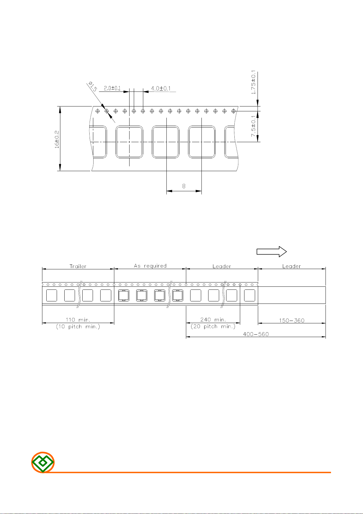
(6) PACKAGING
(6)-1 CARRIER TAPE DIMENSIONS (mm)
(6)-2 TAPING DIMENSIONS (mm)
Unreeling
Direction
MAG.LAYERS
SMB-853025
Page-6/7
Page 7

(6)-3 REEL DIMENSIONS
(6)-4 QUANTITY
500 pcs/Reel
The products are packaged so that no damage will be sustained.
MAG.LAYERS
SMB-853025
Page-7/7
Page 8

TYPICAL ELECTRICAL CHARACTERISTICS
1000
100
Impedance(Ω)
10
1
1 10 100 1000
Frequency(MHz)
MAG.LAYERS
SMB-853025
ATTACHMENT-1
 Loading...