

MagAlpha PCM1704 User Manual
®
PCM1704
49%
PCM1704
FPO
24-Bit, 96kHz
BiCMOS Sign-Magnitude
DIGITAL-TO-ANALOG CONVERTER
FEATURES
● SAMPLING FREQUENCY (fS): 16kHz to 96kHz
● 8X OVERSAMPLING AT 96kHz
● INPUT AUDIO DATA WORD: 20-, 24-Bit
● HIGH PERFORMANCE:
Dynamic Range: K Grade = 112dB typ
SNR: 120dB typ
THD+N: K Grade = 0.0008% typ
● FAST CURRENT OUTPUT: ±1.2mA/200ns
● GLITCH-FREE OUTPUT
● PIN-PROGRAMMABLE DATA INVERSION
● POWER SUPPLY: ±5V
● SMALL 20-LEAD SO PACKAGE
TM
DESCRIPTION
The PCM1704 is a precision, 24-bit digital-to-analog
converter with exceptionally high dynamic performance. The ultra-low distortion and excellent lowlevel signal performance makes the PCM1704 an ideal
candidate for high-end consumer and professional
audio applications. When used with a digital interpolation filter, the PCM1704 supports 8X oversampling
at 96kHz.
The PCM1704 incorporates a BiCMOS sign-magnitude architecture that eliminates glitches and other
nonlinearities around bipolar zero. The PCM1704 is
precision laser-trimmed at the factory to minimize
differential linearity and gain errors.
In addition to high performance audio systems, the
PCM1704 is well-suited to waveform synthesis applications requiring very low distortion and noise.
SBAS097
BCLK
WCLK
DATA
20-BIT
INVERT
REF DC SERVO DC DGND +V
International Airport Industrial Park • Mailing Address: PO Box 11400, Tucson, AZ 85734 • Street Address: 6730 S. Tucson Blvd., Tucson, AZ 85706 • Tel: (520) 746-1111 • Twx: 910-952-1111
Internet: http://www.burr-brown.com/ • FAXLine: (800) 548-6133 (US/Canada Only) • Cable: BBRCORP • Telex: 066-6491 • FAX: (520) 889-1510 • Immediate Product Info: (800) 548-6132
© 1998 Burr-Brown Corporation PDS-1454C Printed in U.S.A. February, 1999
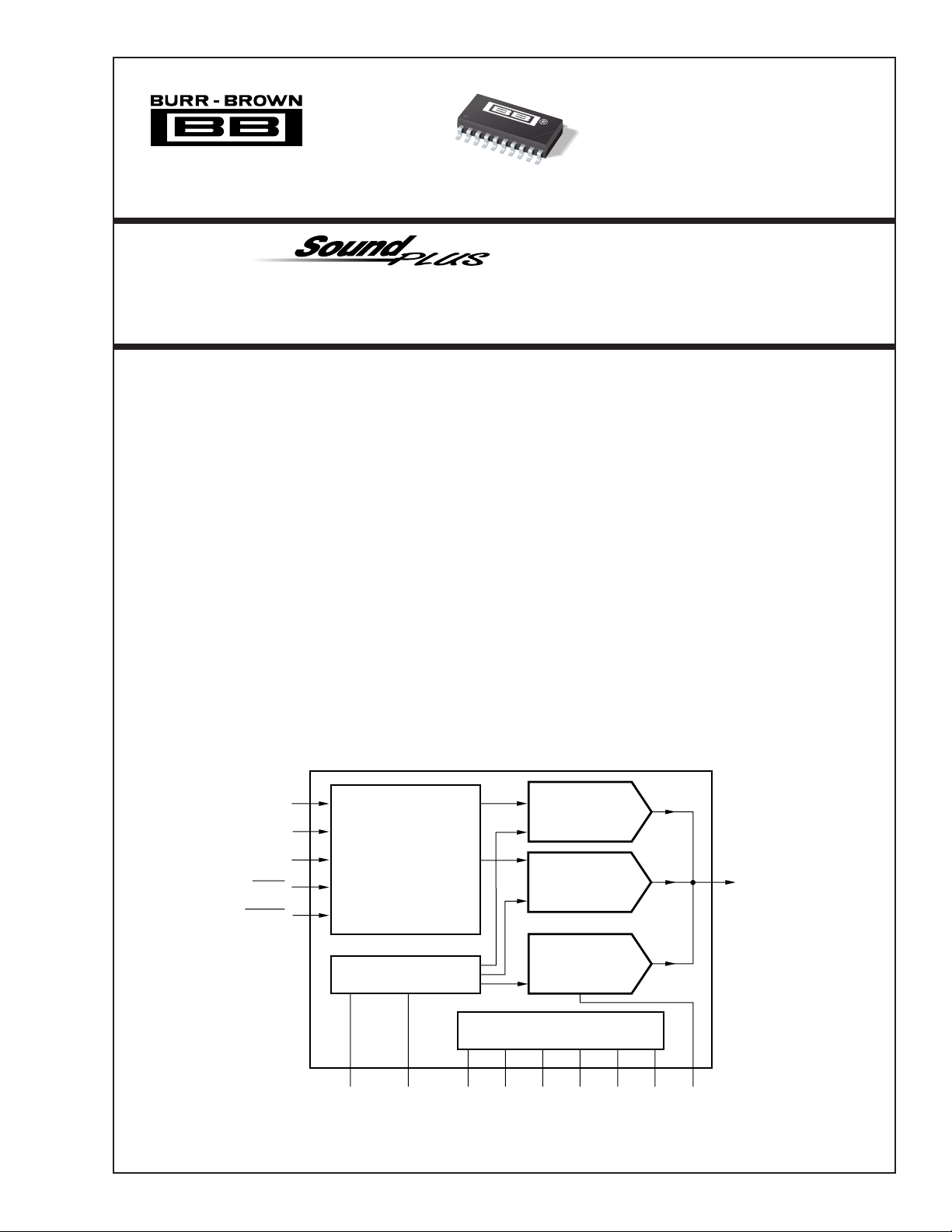
Serial Input
and
Control Logic
Reference and Servo
–V
DD
23-Bit DAC A
23-Bit DAC B I
Bipolar Offset
Power Supply
AGND
DD–VCC
+VCCBPO DC
OUT

SPECIFICATIONS
All specifications at TA = +25°C, ±VCC = ±V
PARAMETER CONDITIONS MIN TYP MAX UNITS
RESOLUTION 24 Bits
DATA FORMAT
Audio Data Interface Format 20-, 24-Bit, MSB-First
Audio Data Code Binary Two’s Complement
Sampling Frequency (f
) 16 96 kHz
S
Input Clock Frequency 25 MHz
DIGITAL INPUT/OUTPUT
Input Logic Level:
(1)
V
IH
(1)
V
IL
(2)
V
IH
(2)
V
IL
Input Logic Current:
(1)
I
IH
(1)
I
IL
(2)
I
IH
(2)
I
IL
DYNAMIC PERFORMANCE(3)
THD+N V
= 0dB PCM1704U 0.0025 0.0030 %
O
V
=–20dB PCM1704U 0.008 0.020 %
O
Dynamic Range EIAJ, A-weighted
Signal-to-Noise Ratio EIAJ, A-weighted 112 120 dB
Low Level Linearity f = 1002Hz at –90dB ±0.5 dB
DC ACCURACY
Gain Error ±1.0 ±3.0 % of FSR
Bipolar Zero Error ±0.5 ±1.0 % of FSR
Gain Drift 0°C to 70°C ±25 ppm of FSR/°C
Bipolar Zero Error Drift 0°C to 70°C ±5 ppm of FSR/°C
ANALOG OUTPUT
Output Range ±1.2 mA
Output Impedance 1.0 kΩ
Settling Time ±0.0003% of FSR, ±1.2mA Step 200 ns
POWER SUPPLY REQUIREMENTS
Voltage Range: +V
Combined Supply Current:+I
= +V
CC
–VCC = –V
DD
DD
CC
–I
CC
TEMPERATURE RANGE
Operation –25 +85 °C
Storage –55 +125 °C
NOTES: (1) BCLK, WCLK, DATA. (2) 20BIT, INVERT. (3) Dynamic performance data is tested with 5534 I/V amp with 7.5kΩ feedback resistor. THD+N data is
tested by Shibasoku 725C with 30kHz external LPF, 400Hz HPF, average mode. Input signal frequency = 1.1kHz.
= ±5V, fS = 768kHz (96kHz • 8), and 24-bit data, unless otherwise noted.
DD
+2.0 +5.0 V
0 +0.8 V
–3.0 0 V
–5.0 –4.2 V
VIH = +V
DD
VIL = 0V ±10 µA
VIH = 0V ±10 µA
VIL = –V
DD
PCM1704U-J 0.0015 0.0025 %
PCM1704U-K 0.0008 0.0015 %
PCM1704U-J 0.007 0.015 %
PCM1704U-K 0.006 0.01 %
PCM1704U, U-J 102 110 dB
PCM1704U-K 106 112 dB
+4.75 +5.0 +5.25 VDC
–4.75 –5.0 –5.25 VDC
+VCC = +VDD = +5.0V 5 8 mA
–VCC = –VDD = –5.0V 30 45 mA
PCM1704U
±10 µA
–100 µA
®
PCM1704
2
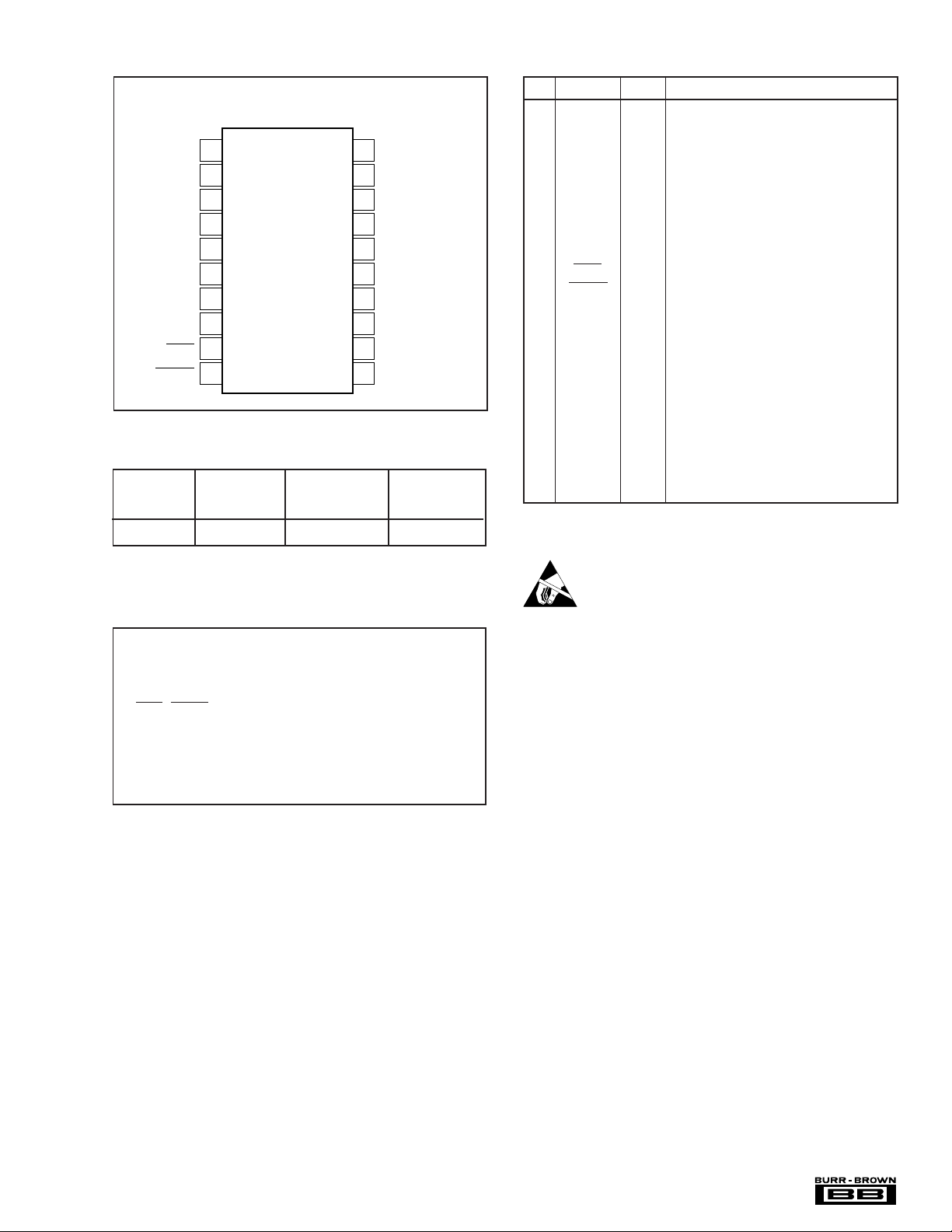
PIN CONFIGURATION
TOP VIEW SOIC
DATA
BCLK
NC
–V
DGND
+V
WCLK
NC
20BIT
INVERT
1
2
3
4
DD
5
6
DD
7
8
9
10
PCM1704U
20
19
18
17
16
15
14
13
12
11
–V
CC
REF DC
NC
SERVO DC
AGND
AGND
I
OUT
NC
BPO DC
+V
CC
PACKAGE INFORMATION
PRODUCT PACKAGE RANGE NUMBER
TEMPERATURE DRAWING
PCM1704U 20-Lead SOIC –25°C to +85°C 248
PACKAGE
PIN ASSIGNMENTS
PIN NAME I/O FUNCTION
1 DATA IN Serial Audio Data Input.
2 BCLK IN Bit Clock Input for Serial Audio Data.
3 NC — No Connection.
4–V
5 DGND — Digital Ground.
6+V
7 WCLK IN Data Latch Enable Input.
8 NC — No Connection.
9 20BIT IN Input Data Word Selection
10 INVERT IN Input Data Polarity Selection
11 +V
12 BPO DC — Bipolar Offset Decoupling Capacitor.
13 NC — No Connection.
14 I
15 AGND — Analog Ground.
16 AGND — Analog Ground.
17 SERVO DC — Servo Amplifier Decoupling Capacitor.
18 NC — No Connection.
19 REF DC — Band Gap Reference Decoupling Capacitor.
(1)
20 –V
NOTE: (1) Internal pull-up resistors. Input level must be a voltage from –V
to DGND.
DD
DD
CC
OUT
CC
— Digital Power, –5V.
— Digital Power, +5V.
(1)
.
(1)
— Analog Power, +5V.
OUT Current Output for Audio Signal.
— Analog Power, –5V.
.
DD
NOTE: (1) For detailed drawing and dimension table, please see end of data
sheet, or Appendix C of Burr-Brown IC Data Book.
ABSOLUTE MAXIMUM RATINGS
Supply Voltage, +VDD ,+VCC............................................................. +6.5V
Supply Voltage Differences .............................................................. ±0.1V
GND Voltage Differences ................................................................. ±0.1V
Digital Input Voltage
(BCLK, WCLK, DATA) ............................ DGND –0.3V to (+V
(20BIT, INVERT).................................... –V
Input Current (any pins except supply pins) ................................... ±10mA
Power Dissipation .......................................................................... 300mW
Operating Temperature Range ......................................... –25°C to +85°C
Storage Temperature...................................................... –55°C to +125°C
Lead Temperature (soldering, 5s) ................................................. +260°C
Package Temperature (reflow, 10s) .............................................. +235°C
– 0.3V to (DGND + 0.3V)
DD
+ 0.3V)
DD
ELECTROSTATIC
DISCHARGE SENSITIVITY
This integrated circuit can be damaged by ESD. Burr-Brown
recommends that all integrated circuits be handled with
appropriate precautions. Failure to observe proper handling
and installation procedures can cause damage.
ESD damage can range from subtle performance degradation
to complete device failure. Precision integrated circuits may
be more susceptible to damage because very small parametric
changes could cause the device not to meet its published
specifications.
3 PCM1704
®
SPECIFICATIONS
All specifications at +25°C, ±VCC and ±VDD = ±5.0V, unless otherwise noted.
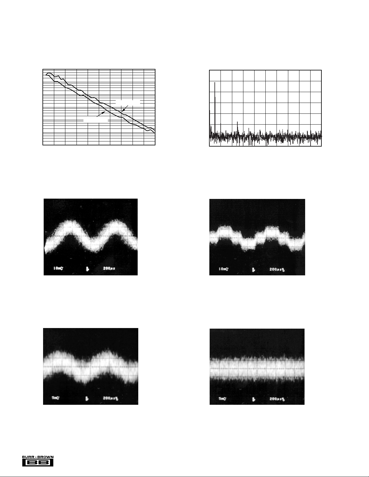
100
10
1
0.1
THD+N (%)
0.10
0.001
0.0001
–100 –90 –80 –70 –60 –40 –30 –10–20–50
THD+N vs LEVEL
24-Bit Data
Output Level (dBFS)
DAC OUTPUT
–110dB, 24-Bit, 96kHz
16-Bit Data
0
–20
–40
–60
THD+N (dB)
–80
–100
–120
0
–80
–90
–100
–110
–120
Amplitude (dB)
–130
–140
–150
20.0 2.02k 4.02k 6.01k 8.01k 10.0k 12.0k 14.0k 16.0k 18.0k 20.0k
–90dB SIGNAL SPECTRUM
Output Frequency (Hz)
DAC OUTPUT
–110dB, 20-Bit, 96kHz
–120dB, 24-Bit, 96kHz
®
PCM1704
DAC OUTPUT
DAC OUTPUT
–120dB, 20-Bit, 96kHz
4
 Loading...