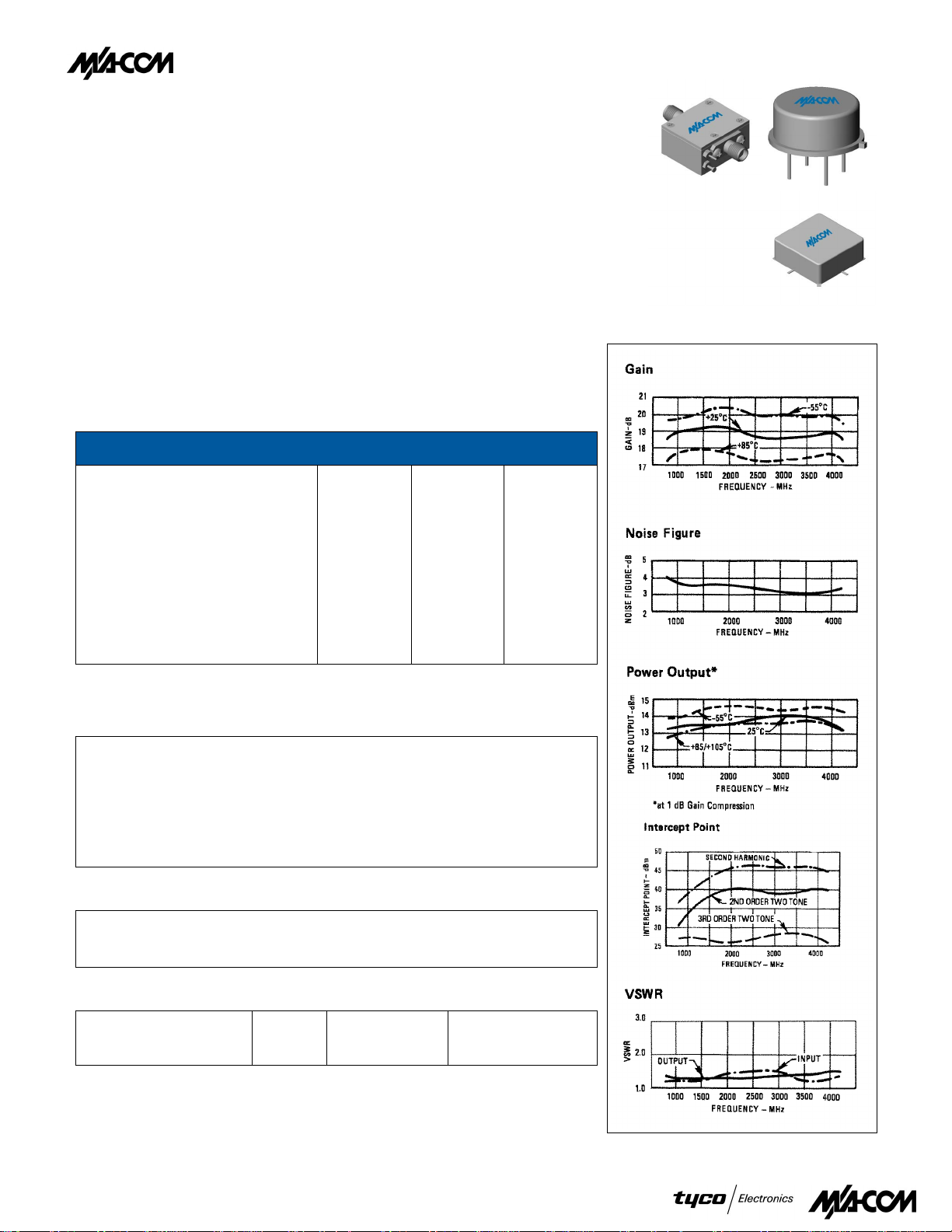
M A COM manufacturer of RF CA45-1, A45-1 Datasheet

· WIDE BANDWIDTH
· HIGH GAIN 17.5 dB (TYP.)
· LOW NOISE: 4.1 dB (TYP.)
· GaAs FET DESIGN
A45-1/SMA45-1
1000 TO 4000 MHz
Specifications (Rev. Date: 1/01)*
* Measured in a 50-ohm system at +5 Vdc Nominal. Subject to change without notice.
BG
AA
CE
0.8-4.2 GHz
17.5 dB
±0.6 dB
36 dB
4.0 dB
13.0 dBm
+26 dBm
+33 dBm
+40 dBm
1.8:1 / 1.8:1
65 mA
1.0-4.0 GHz
16.5 dB
±0.8 dB
12.0 dBm
5.0 dB
12.5 dBm
2.0:1 / 2.0:1
80 mA
1.9:1 / 1.9:1
75 mA
1.0-4.0 GHz
15.5 dB
±1.0 dB
5.5 dB
-65° to +125°C
125°C
+6 Volts
+13 dBm
100 mW
0.25 W
125°C
132°C/W
0.171 W
23°C
A45-1
SMA45-1
CA45-1
Frequency
Small Signal Gain (min.)
Gain Flatness (max.)
Reverse Isolation
Noise Figure (max.)
Power Output @ 1 dB comp. (min.)
IP3
IP2
Second Order Harmonic IP
VSWR Input / Output (max.)
DC Current @ 15 Volts (max.)
0
°°°°
to 50
Guaranteed Characteristics Typical
°°°°
C -54
°°°°
to +85
Typical Performance @ 25°C
°°°°
C
Absolute Maximum Ratings
Storage Temperature
Max. Case Temperature
Max. DC Voltage
Max. Continuous RF Input Power
Max. Short Term RF Input Power (1 minute max.)
Max. Peak Power (3 µsec max.)
“S” Series Burn-in Temperature (Case)
Thermal Data: Vcc = 15 Vdc
Thermal Resistance
Transistor Power Dissipation P
Junction Temperature Rise Above Case T
θ
jc
d
jc
Outline Drawings
Package TO-8 Surface Mount SMA Connectorized
Figure
Model
Specifications subject to change without notice. • North America: 1-800-366-2266
Visit www.macom.com for complete contact and product information.
 Loading...