M A COM V42100TR, V42100 Datasheet

Surface Mount Voltage Controlled Oscillator V42100
M/A-COM Division of AMP Incorporated ■ North America: Tel. (800) 366-2266, Fax (800) 618-8883 ■ Asia/Pacific: Tel.+85 2 2111 8088,
Fax +85 2 2111 8087
■
Europe: Tel. +44 (1344) 869 595, Fax+44 (1344) 300 020
www .macom.com
AMP and Connecting at a Higher Level are trademarks.
Specifications subject to change without notice.
V2.00
Features
•
Miniature SMT Package
•
Low Phase Noise
•
Highly Linear Tuning
•
+3V Operation
Description
The V42100 is a fundamental single ended oscillator designed for
use in cost sensitive wireless applications. The VCO integrates a
bipolar transistor, varactor diode and high Q resonator in a surface
mount package. The standard SMT packaging provides electrical
shielding and easy PCB assembly. The circuit design and component device selection have been optimised for low phase noise
and highly linear tuning performance.
M/A-COM VCOs are manufactured in facilities using advanced
surface mount assembly and automated electr ical test equipment.
This ensures consistent electrical performance and product quality
over volume manufacturing quantities.
Electrical Specifications1, TA = +25°C, VCC = +3V
(unless otherwise stated)
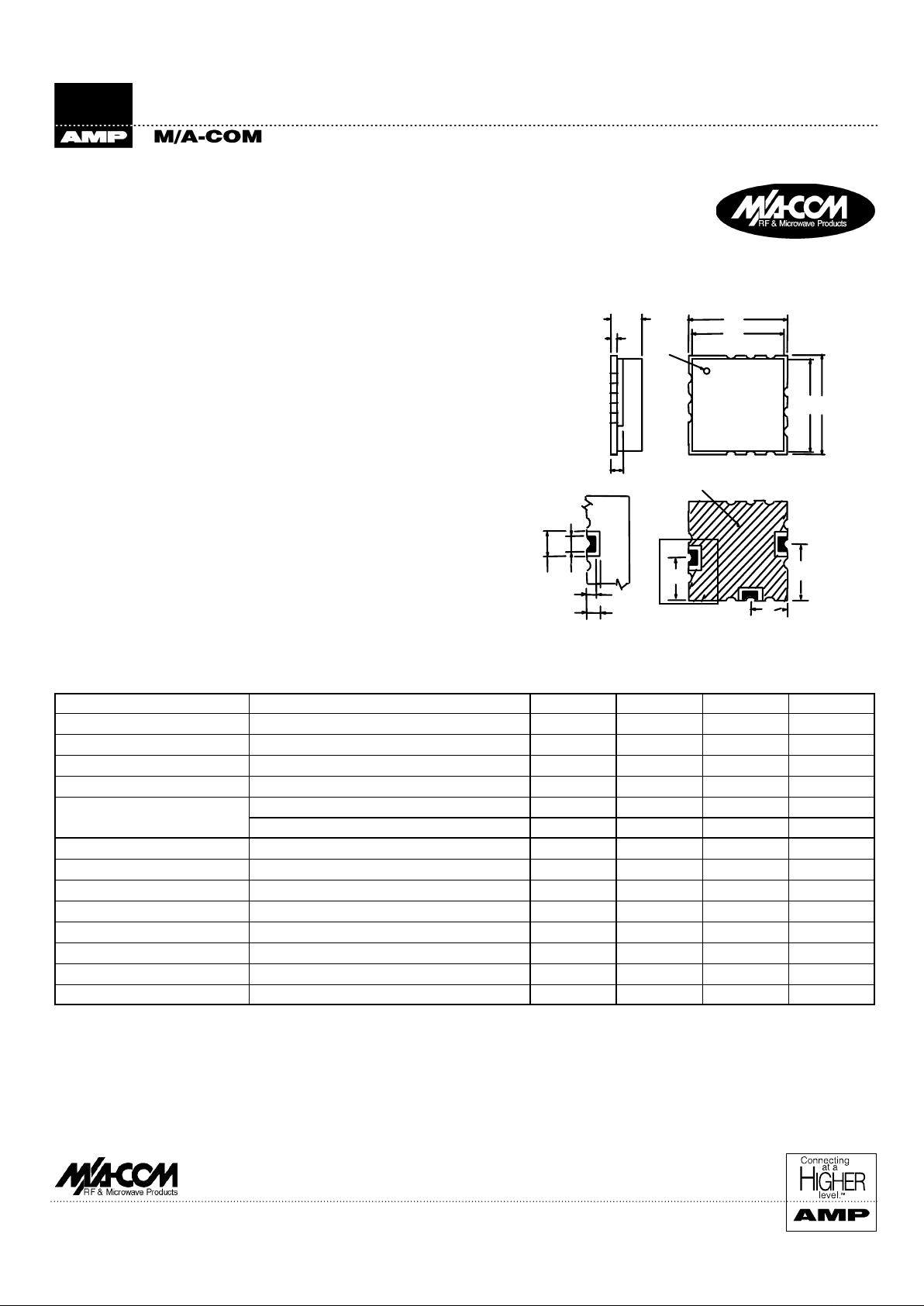
LSM4 Package
4. Non harmonic spurious less than -70 dBc.
5. See plot for typical phase noise at other offset freque ncies.
6. Defined as (2150 - 2050) / (V
T
2150 - VT 2050) MHz/V.
7. The max/min ratio of tuning sensitivity over F
OUT
, see plot for typi-
cal tuning linearity measured over 0.5V intervals
1. All specification limits are indicated values and apply over F
OUT
and
for 50 Ω load impedance.
2. Tuning voltages shown are the minimum and maximum voltages
required to tune the frequency range, including temperature effects
over 0°C to +70°C. Devices will oscillate normally with tuning voltages from 0V to +6V.
3. Output power window includes variation over operating temperature
range (T
OP
) 0°C to +70°C and output frequency range (F
OUT
).
Surface Mount Voltage Controlled Oscillator
WLAN 2050 - 2150 MHz
V42100
1
DETAIL A.
0.5
2.0
1.3
4.6
3.0
3.0
7.6
DETAIL A.
7.6
VT
VCC
RF
6.9
6.9
IDENT
M/ A- COM
PART NO.
PLATED AREA
0.7
1.3
1.0
2.0
3
1
2
Parameter Test Conditions Units Min. Typ. Max.
Frequency Range (F
OUT
)
Over T
OP
MHz 2050 2150
Tuning Voltage (V
T
)
2
Over T
OP
V +0.6 +4.0
RF Output Power (P
OUT
)
3
Over T
OP
dBm +5.0 +10.0
Harmonic Output
4
dBc -20
Phase Noise
5
SSB at 10 kHz offset from carrier dBc/Hz -87 -82
SSB at 100 kHz offset from carrier dBc/Hz -108 -103
Average Tuning Sensitivity
6
MHz/V 100
Tuning Linearity
7
Ratio 1.4
Frequency Pushing
V
CC
+3V ± 0.15V
MHz/V 5 10
Frequency Pulling
Over all phases of a 1.14:1 VSWR load MHz 10 12
Frequency Drift
Over T
OP
MHz/°C
-0.51
Tune Input Capacitance
pF 50
Supply Current (I
CC
)
mA 13 18
Supply Voltage (V
CC
) Recommended operating limit V +2.85 +3.15

Surface Mount Voltage Controlled Oscillator V42100
M/A-COM Division of AMP Incorporated ■ North America: Tel. (800) 366-2266, Fax (800) 618-8883 ■ Asia/Pacific: Tel.+85 2 2111 8088,
Fax +85 2 2111 8087
■
Europe: Tel. +44 (1344) 869 595, Fax+44 (1344) 300 020
www .macom.com
AMP and Connecting at a Higher Level are trademarks.
Specifications subject to change without notice.
V2.00
Absolute Maximum Ratings
1, 2
Environmental Specifications
Devices are designed to function over the operating temperature
range (T
OP
) of 0°C to +70°C and after exposure to the shock,
vibration, thermal shock and moisture conditions typically encountered in base station and subscriber terminal environments.
Functional Configuration
Substrate material is RO4003.
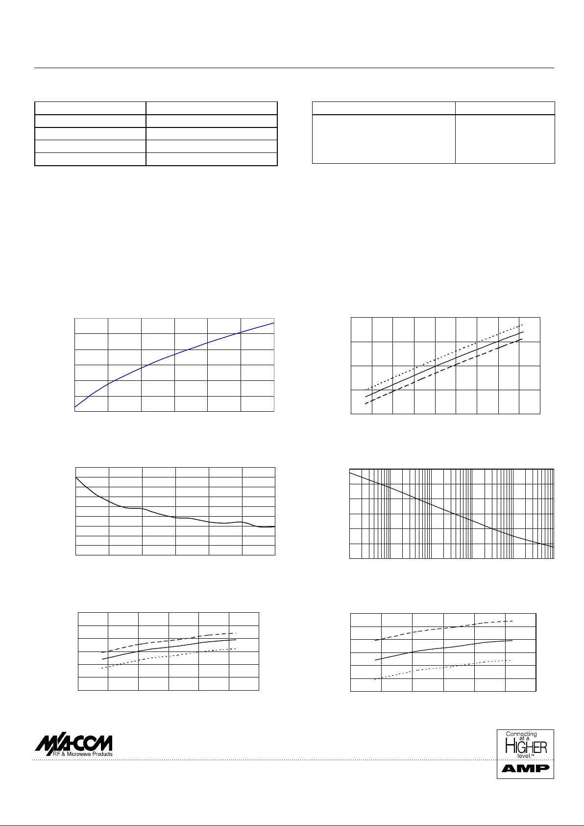
Typical Performance
Tuning Curve vs Temperat ure
Tuning Curve
Output Power vs Supply Volta ge (Vc c)Output Power vs Temperat ur e
Pin Function
1 Tuning Voltage (V
T
)
2RF Output
3 Supply Voltage (V
CC
)
Case/Lid Ground
Parameter Absolute Maximum
Tuning Voltage (V
T
) 0V to +9V
Supply Voltage
(VCC)
3
+5V
Storage Temperature (T
STOR
) -45°C to +125°C
Solder Assembly Temperature See App Note M2032
1. Exceeding these limits may cause permanent damage.
2. Static sensitive, observe appropriate handling precautions.
3. An external series resistor and bypass capacitor will allow operation
at higher supply voltage and will improve power supply decoupling
and noise suppression.
Ordering Information
VCOs are available in either tape and r eel or tube packaging. To
order devices in tape and reel requires the suffix TR be added to
the part number, i.e. V42100TR. Quantity 1500 per 13 inch reel,
see Application Note M2037.
Phase NoiseTuning Linearity
2.4
2.3
2.2
2.1
2.0
1.9
1.8
0.0 1.0 2.0 3.0 4.0 5.0 6.0
TUNING VOLTAGE (V)
FREQUENCY (GHz)
2.20
2.15
2.10
2.05
2.00
1.4 1.6 1.8 2.0 2.2 2.4 2.6 2.8 3.0 3.2
TUNING VOLTAGE (V)
FREQUENCY (GHz)
180
160
140
120
100
80
60
40
20
0
0.0 1.0 2.0 3.0 4.0 5.0 6.0
TUNING VOLTAGE (V)
TUNING SENSITIVITY (MHz/V)
-40
-60
-80
-100
-120
-140
-160
100 1K 10K 100K 1M 10M
FREQUENCY OFFSET FROM CARRIER (Hz)
PHASE NOISE (dBc/Hz)
10.0
9.0
8.0
7.0
6.0
5.0
4.0
1.95 2.00 2.05 2.10 2.15 2.20 2.25
FREQUENCY (GHz)
OUTPUT POWER (dBm)
10.0
9.0
8.0
7.0
6.0
5.0
4.0
1.95 2.00 2.05 2.10 2.15 2.20 2.25
FREQUENCY (GHz)
OUTPUT POWER (dBm)
+70° C
+25° C
0° C
0° C
+25° C
+70° C
3.15 V
3.00 V
2.85 V
 Loading...