M A COM SW65-0014TR, SW65-0014-TB Datasheet

GaAs SPST Absorptive Switch with
V 5.00
ASIC Driver, DC - 3.0 GHz
SW65-0014
Features
n Typical Isolation: 42 dB (2,000 MHz)
n Typical Insertion Loss: 1.8 dB (2,000 MHz)
n Integral ASIC TTL/CMOS Driver
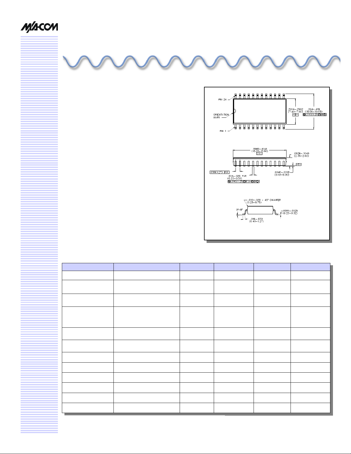
n Plastic, 50 mil Pitch, SOW-24 Lead, Wide Body
n Low DC Power Consumption
n 50 Ohm Nominal Impedance
n Tape and Reel Packaging Available
n Test Boards Available
Description
M/A-COM's SW65-0014 is a GaAs MMIC absorptive
SPST switch with an integral silicon ASIC driver. This
device is in a 24-lead plastic package. This switch offers
excellent broadband performance and repeatability from
DC to 3 GHz, while maintaining low DC power dissipation.
The SW65-0014 is ideally suited for wireless infrastructure
applications. Also available in ceramic package with
improved performance.
SOW-24
Package outline conforms to JEDEC standard MS-013AD.
Electrical Specifications: TA = 25°C
Parameter Test Conditions Units Min Typical Max
Insertion Loss DC - 3.0 GHz dB — 1.8 2.2
Isolation
(All arms off)
VSWR
T
T
rise
Ton T
Transients
1 dB Compression .05 GHz
Input IP3 Two tone inputs 0.05 GHz
Logic “0” Iin = 20 µA max V 0.0 — 0.8
Logic “1” Iin = 20 µA max V 2.0 — 5.0
1. Decoupling capacitors (.01 µF) are required on the power supply lines.
fall
off
VCC — V +4.5 +5.0 +5.5
VEE — V -8.0 -5.0 -4.75
ICC VCC = +5.0V mA — — 4
IEE VEE = -5.0V mA — — -1
DC - 3.0 GHz dB 35 42 —
DC - 3.0 GHz
10%/90%, 90%/10%
50% TTL to 90%/10% RF
In-band (peak to peak)
.5 - 3.0 GHz
Up to +5 dBm 0.5 - 3.0 GHz
1
—
nS
nS
mV
dBm
dBm
dBm
dBm
—
—-
—
—
—
—
—
—
On Off
1.6:1 2.0:1
15
50
50
+20
+27
+35
+46
2.1:1
50
150
150
—
—
—
—

GaAs SPST Absorptive Switch with ASIC Driver, DC - 3.0 GHz
SW65-0014
V 5.00
2,3
Parameter Absolute Maximum
Max. Input Power
0.05 GHz
0.5 - 3.0 GHz
VEE
VCC
Control Voltage 4
2. Operation of this device above any one of these parameters
3. When the RF input is applied to the terminated port, the
4. Standard CMOS TTL interface, latch-up will occur if logic
Bias Voltages
-0.5V to VCC +0.5V
Operating Temperature -40°C to +85°C
Storage Temperature -65°C to +125°C
may cause permanent damage.
absolute maximum power is +30 dBm.
signal is applied prior to power supply.
+27 dBm
+34 dBm
-8.5V
+5.5V
Truth Table
TTL Control Input RF Common To:
C1 RF1
1 On
0 Off
Pin Configuration Absolute Maximum Ratings
Pin # Function Pin # Function
1 RFc 13 C1
2 GND 14 GND
3 GND 15 GND
4 GND 16 GND
5 GND 17 GND
6 GND 18 GND
7 GND 19 RF1
8 V
9 GND 21 GND
10 V
11 GND 23 GND
12 GND 24 GND
EE
CC
20 GND
22 GND
Ordering Information
Part Number Package
SW65-0014 Bulk Packaging
SW65-0014TR Tape and Reel (1K Reel)
SW65-0014-TB Units Mounted on Test Board
Specifications subject to change without notice.
n North America: Tel. (800) 366-2266
n Asia/Pacific: Tel.+81-44-844-8296, Fax +81-44-844-8298
n Europe: Tel. +44 (1344) 869 595, Fax+44 (1344) 300 020
Visit www.macom.com for additional data sheets and product information.
2
 Loading...