M A COM SW65-0003TR, SW65-0003-TB, SW65-0003 Datasheet

GaAs SP8T Reflective Switch,
DC - 2500 MHz
V 3.00
SW65-0003
Features
n Cascadable Port
n Building Block for Switch Matrics
n 23 dB Isolation at 2.5 GHz
n Low DC Power Consumption
n Terminated Common Port
n 50 Ohm Nominal Impedance
Description
M/A-COM’s SW65-0003 is a GaAs MMIC SP8T reflective
switch in a SMT plastic package. The switch has a low loss
growth port, J9, that allows for cascading the device into
larger multi-throw switches. It can be configured for
common arm, J0, match when all the output ports are in
isolation. The switch offers excellent broadband
performance and repeatability from DC to 2.5 GHz, while
maintaining low DC power dissipation. The SW65-0003 is
ideally suited for switch matrix and high volume wireless
infrastructure and applications.
Electrical Specifications: TA = 25°C
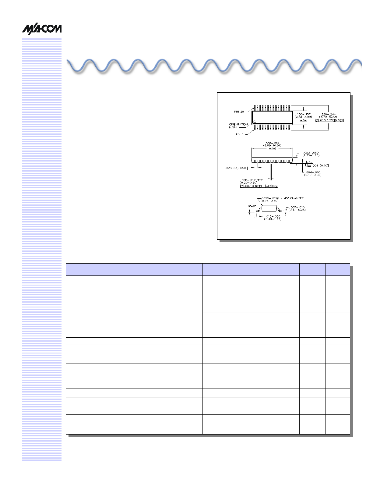
QSOP-28
Package Outline conforms to JEDEC Standard MO-137AF.
Parameter Test Conditions Frequency Units Min. Typ. Max.
Insertion Loss DC - 1.0 GHz
Insertion Loss J9 Port
Isolation
Isolation J9 Port DC - 1.0 GHz
VSWR Input (J0) DC - 2.5 GHz Ratio — 1.2:1 1.5:1
VSWR (All arms off) DC - 1.0 GHz
VSWR Output DC - 1.0 GHz
VSWR (J9) DC - 1.0 GHz
Switching Speed 90% / 10% or 10% / 90% RF nSec — 3 10
1 dB Compression Input Power — dBm +20 +22 —
Input IP2 Two tone inputs to +5 dBm — dBm +65 — —
Input IP3 Two tone inputs to +5 dBm — dBm +45 — —
DC Bias 0V
-5V
DC - 2.0 GHz
DC - 2.5 GHz
DC - 1.0 GHz
DC - 2.0 GHz
DC - 2.5 GHz
DC - 1.0 GHz
DC - 2.5 GHz
DC - 2.5 GHz
DC - 2.0 GHz
DC - 2.5 GHz
DC - 2.5 GHz
DC - 2.5 GHz
—
—
dB
dB
dB
dB
dB
dB
dB
dB
dB
dB
Ratio
Ratio
Ratio
Ratio
Ratio
Ratio
Ratio
µA
µA
—
—
—
—
—
—
28
20
22
15
—
—
—
—
—
—
—
—
—
1.7
2.0
2.5
1.0
1.4
2.0
31
23
25
18
1.1:1
1.8:1
2.0:1
1.2:1
1.3:1
1.0:1
1.3:1
—
—
2.0
2.3
2.8
1.3
1.7
2.3
—
—
—
—
1.4:1
2.1:1
2.3:1
1.5:1
1.6:1
1.3:1
1.6:1
10
100

GaAs SP8T Reflective Switch, DC - 2500 MHz
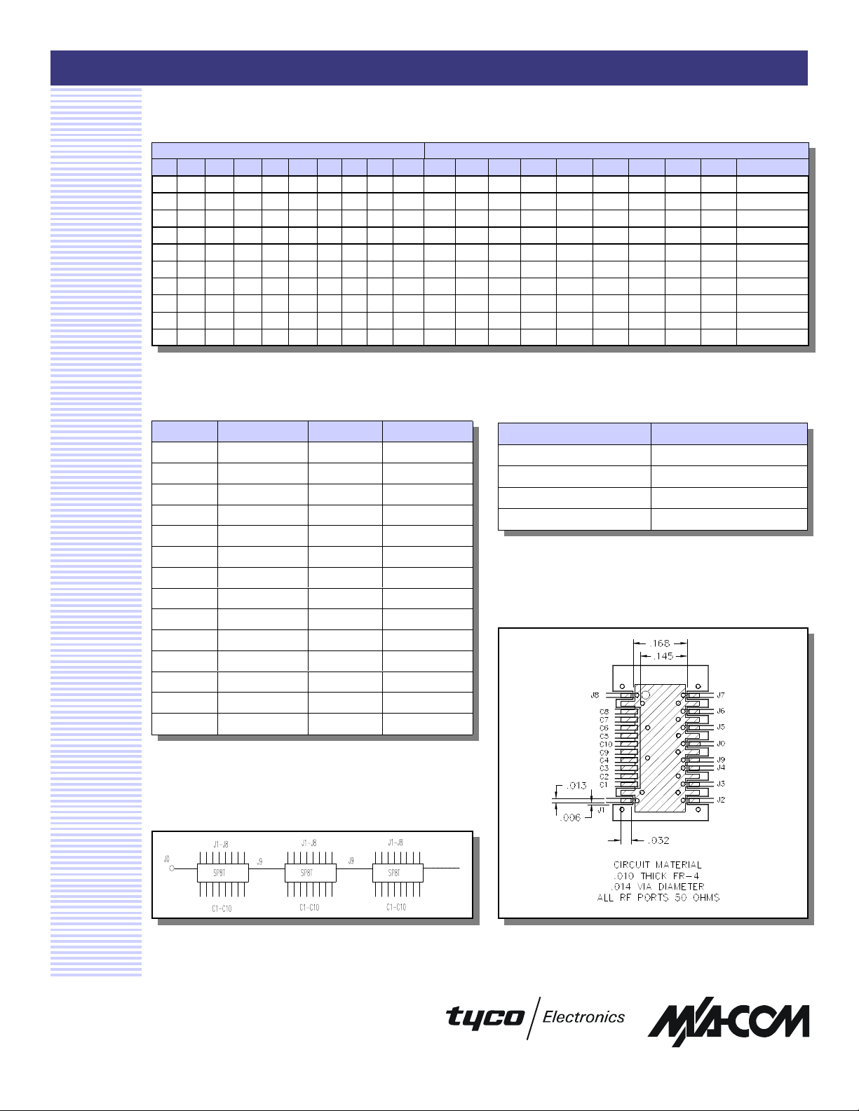
Truth Table
Control Inputs
C1 C2 C3 C4 C5 C6 C7 C8 C9 C10 J1 J2 J3 J4 J5 J6 J7 J8 J9 J10 Match
L H H H H H H H H H On Off Off Off Off Off Off Off Off Off
H L H H H H H H H H Off On Off Off Off Off Off Off Off Off
H H L H H H H H H H Off Off On Off Off Off Off Off Off Off
H H H L H H H H H H Off Off Off On Off Off Off Off Off Off
H H H H L H H H H H Off Off Off Off On Off Off Off Off Off
H H H H H L H H H H Off Off Off Off Off On Off Off Off Off
H H H H H H L H H H Off Off Off Off Off Off On Off Off Off
H H H H H H H L H H Off Off Off Off Off Off Off On Off Off
H H H H H H H H L H Off Off Off Off Off Off Off Off On Off
H H H H H H H H H L Off Off Off Off Off Off Off Off Off On
VIN Low = 0 to -0.2V @ 10µA VIN High = -5V @ 90µA
SW65-0003
V 3.00
Condition of Switch
Pin Configuration
Pin No. Function Pin No. Function
1 J8 15 J2
2 Ground 16 Ground
3 C8 17 J3
4 C7 18 Ground
5 C6 19 J4
6 C5 20 J9
7 C10 21 Ground
8 C9 22 J0
9 C4 23 Ground
10 C3 24 J5
11 C2 25 Ground
12 C1 26 J6
13 Ground 27 Ground
14 J1 28 J7
Cascadable Application
Absolute Maximum Ratings 1
Parameter Absolute Maximum
Input Power +34 dBm
Control Voltage -8.5 volts
Storage Temperature -65°C to +125°C
Operating Temperature -40° to +85°C
1. Operation of this device above any one of these
parameters may cause permanent damage.
PCB Layout
Specifications subject to change without notice.
n North America: Tel. (800) 366-2266
n Asia/Pacific: Tel.+81-44-844-8296, Fax +81-44-844-8298
n Europe: Tel. +44 (1344) 869 595, Fax+44 (1344) 300 020
Visit www.macom.com for additional data sheets and product information.
2
 Loading...