GaAs SPDT Switch
DC - 3.0 GHz
SW-456
Features
n Low Cost Plastic SC-70 (SOT-363) Package
n Low Insertion Loss < 0.3 dB @ 900 MHz
n Low Power Consumption < 15 µA @ +2.3 Volts
n Positive or Negative 2.3 to 8 Volt Control
Description
M/A-COM’s SW-456 is a GaAs monolithic switch in a low
cost SC-70 (SOT-363) surface mount plastic package. The
SW-456 is ideally suited for applications where very low
power consumption, low insertion loss, very small size and
low cost are required. Typical application is in dual band
systems where switching between small signal components
is required such as filter banks, single-band LNA’s,
converters, etc. The SW-456 can be used in applications up
to 0.25 watts in systems such as cellular, PCS, DCS1800,
GSM, CDMA, W-CDMA and other analog/digital wireless
communication systems.
The SW-456 is fabricated using a mature 0.8 micron GaAs
MESFET process. The process features full passivation for
performance and reliability.
Handling Procedures
The following precautions should be observed to avoid
damage:
Static Sensitivity
Gallium Arsenide Integrated Circuits are ESD sensitive
and can be damaged by static electricity. Proper ESD
techniques should be used when handling these devices.
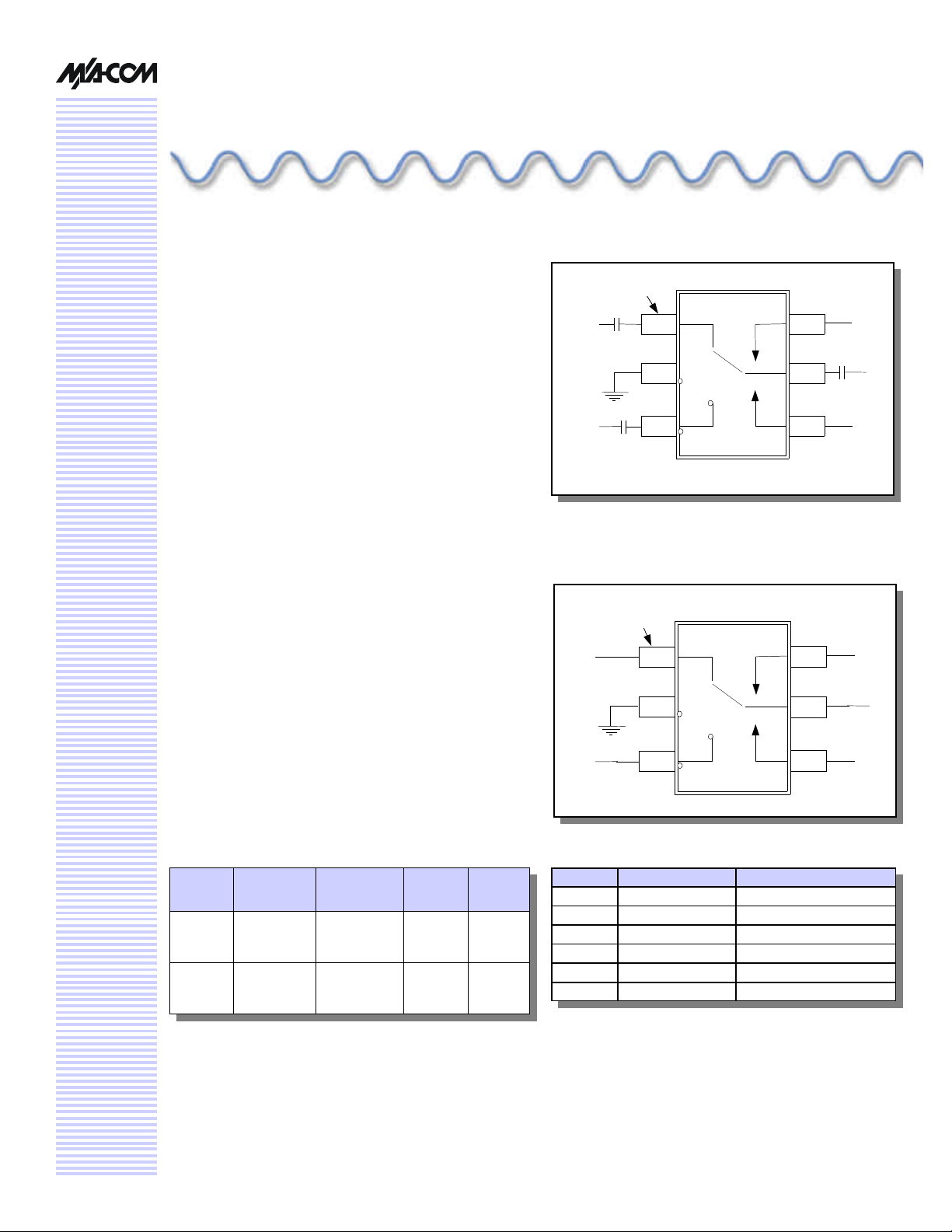
Functional Schematic
Positive Control Voltage
PIN 1
RF1
1000 pF
GND
RF2
1000 pF
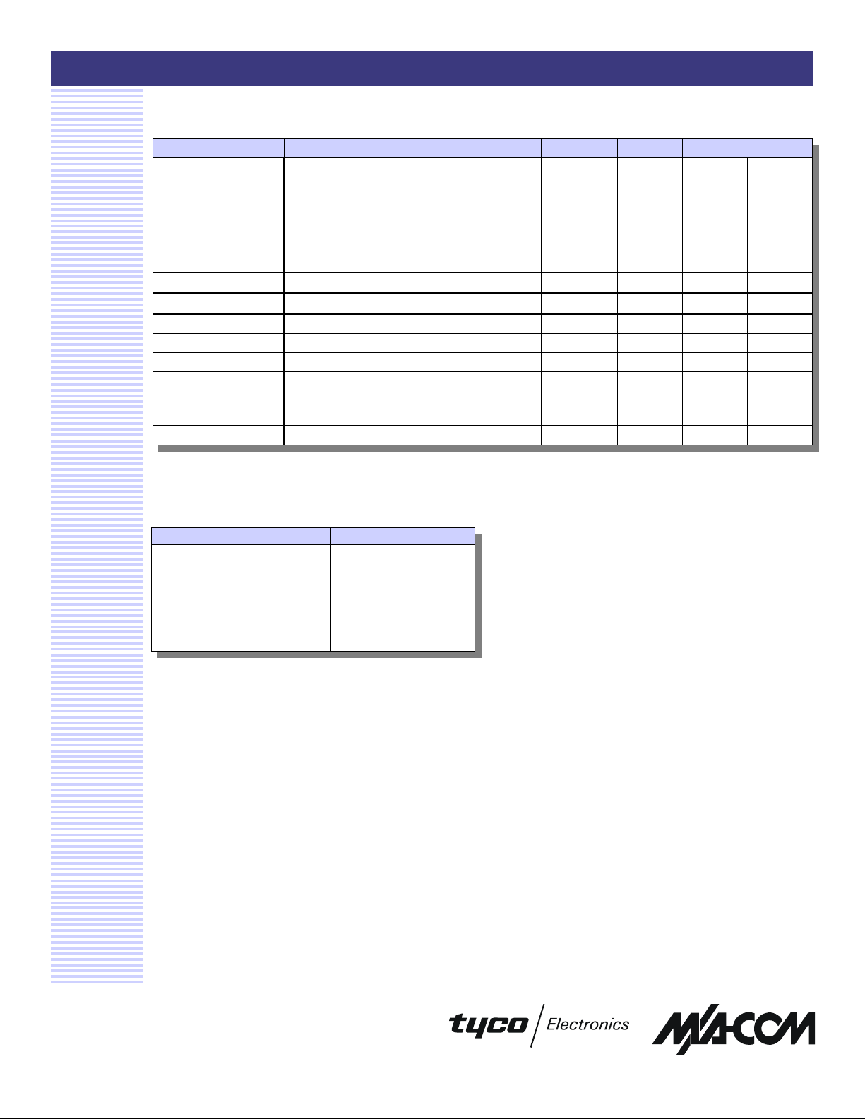
Functional Schematic
Negative Control Voltage
PIN 1
RF1
GND
RF2
V1
RFC
1000 pF
V2
V1
RFC
V2
Truth Table
Mode
(Control)
Positive1 0 ± 0.2 V +2.3 to +8 V Off On
+2.3 to +8 V 0 ± 0.2 V On Off
Negative2 0 ± 0.2 V -2.3 V to –8 V On Off
-2.3 V to -8 V 0 ± 0.2 V Off On
1. External DC blocking capacitors are required on all RF
ports. 1000 pF capacitors used for positive control voltage.
For higher frequency operation, smaller value DC blocking
capacitors can be substituted.
2. If negative control is used, DC blocking capacitors are not
required on RF ports.
V1 V2 RFC -
RF1
RFC -
RF2
PIN Configuration
PIN Function Description
1 RF1 RF In/Out
2 GND RF Ground
3 RF2 RF In/Out
4 V2 V
5 RFC RF Common
6 V1 V
CTRL2
CTRL1

GaAs SPDT Switch, DC - 3.0 GHz
SW-456
V 2.00
Electrical Specifications: T
Parameter Test Conditions Units Min. Typ. Max.
Insertion Loss DC - 1 GHz dB 0.35 0.5
1 - 2 GHz dB 0.45 0.6
2 - 3 GHz dB 0.56 0.8
Isolation DC - 1 GHz dB 20 22
1 - 2 GHz dB 15 17
2 - 3 GHz dB 10 12
V
DC - 3 GHz 1.2:1 1.4:1
SWR
P
(2.3V supply) 500 MHz - 3 GHz dBm 21
1dB
P
(3V supply) 500 MHz - 3 GHz dBm 27
1dB
Input IP2 2-Tone 900 MHz, 5 MHz spacing (3.0 V) dBm 81
Input IP3 2-Tone 900 MHz, 5 MHz spacing (3.0 V) dBm 52
TRISE, TFALL
TON, TOFF
Transients
Gate Leakage V
10% to 90% RF, 90% to 10% RF ns 25
50% Control to 90% RF, Control to 10% RF ns 25
In-Band mV 25
= 2.3 V
CTL
= 25 °C, V
A
= 0, -2.3 volts (unless otherwise specified)
CTL
µA
4 15
Absolute Maximum Ratings1
Parameter Absolute Maximum
Max Input Power (0.5 - 3.0 GHz)
3 V Control
5 V Control +33 dBm
Operating Voltage +8.5 volts
Operating Temperature
Storage Temperature
+30 dBm
-40 °C to +85 °C
-65 °C to +150 °C
1. Exceeding any one or combination of these limits may cause
permanent damage.
Specifications subject to change without notice.
n North America: Tel. (800) 366-2266, Fax (800) 618-8883
n Asia/Pacific: Tel.+81-44-844-8296, Fax +81-44-844-8298
n Europe: Tel. +44 (1344) 869 595, Fax+44 (1344) 300 020
Visit www.macom.com for additional data sheets and product information.
2
 Loading...