M A COM SW-419TR, SW-419RTR, SW-419 Datasheet

GaAs SP4T Terminated Switch
DC - 2 GHz S W- 4 1 9
Features
● Very Low Power Consumption: 100 µW
● Low Insertion Loss: 1 dB
● High Isolation: 25 dB up to 2 GHz
● Very High Intercept Point: 46 dBm IP
● Nanosecond Switching Speed
● Temperature Range: -40˚C to +85˚C
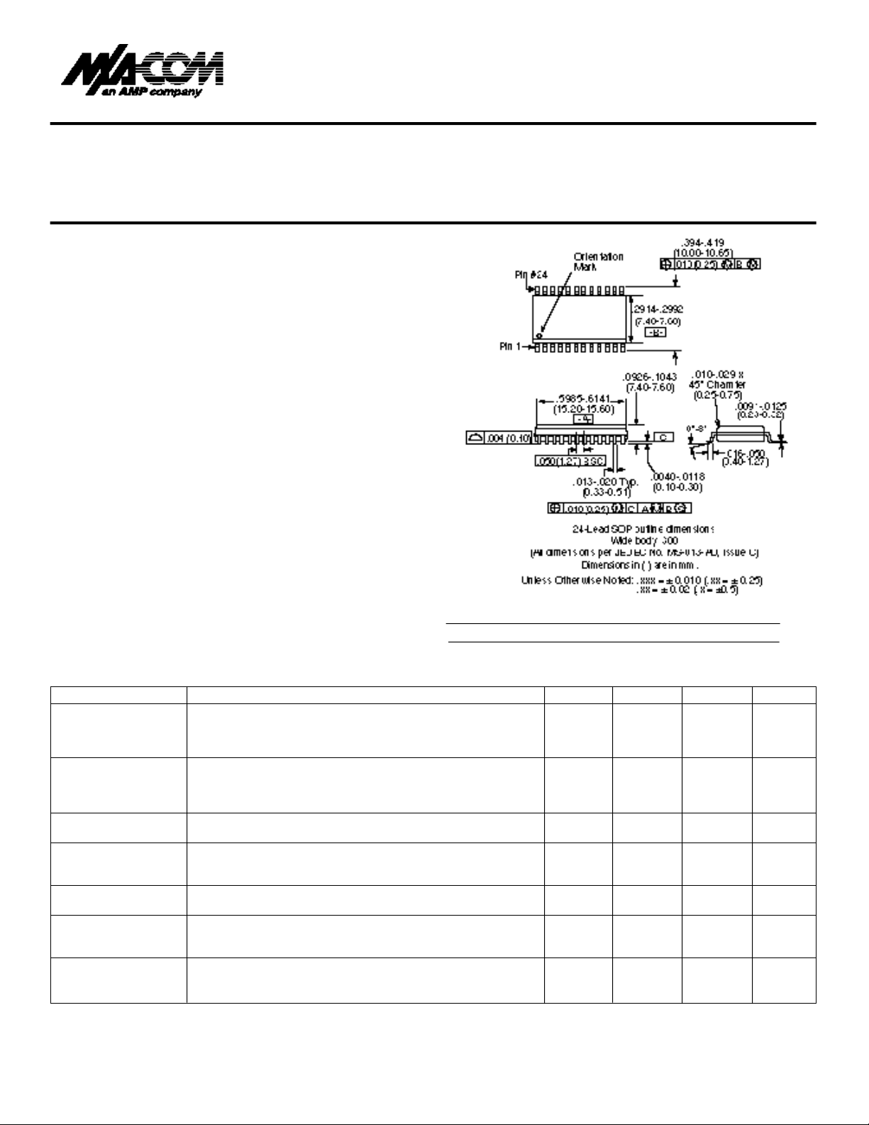
● Low Cost SOIC24 Plastic Package
● Tape and Reel Packaging Available
3
1
SO-24
Description
M/A-COM’s SW-419 is a GaAs MMIC SP4T terminated switch in a
low cost SOIC 24-lead wide body surface mount plastic package.
The SW-419 is ideally suited for use where very low power consumption is re q u i red. Typical applications include switch matrices, and filter banks in systems such as: radio and cellular equipment, PCM, GPS, fiber optic modules, and other battery powere d
radio equipment.
The SW-419 is fabricated with a monolithic GaAs MMIC using a
m a t u re 1-micron process. The process features full chip passivation for increased perf o rmance and re l i a b i l i t y .
Electrical Specifications,TA= +25°C
Parameter Test Conditions
Insertion Loss DC – 0.1 GHz dB 0.8 1.0
Isolation DC – 0.1 GHz dB 54 60
VSWR On 1.3:1
Trise, Tfall 10% to 90% RF, 90% to 10% RF nS 8
Ton, Toff 50% Control to 90% RF, 50% Control to 10% RF nS 16
Transients In Band mV 15
One dB Input Power 0.05 GHz dBm 21
Compression Input Power 0.5 – 2.0 GHz dBm 27
IP
2
IP
3
1. Refer to “Tape and Reel Packaging”Section, or contact factory.
2. All measurements with 0, -5 V control voltages at 1 GHz in a 50Ω system, unless otherwise specified.
Off 1.3:1
Measured Relative 0.05 GHz dBm 45
to Input Power 0.5 – 2.0 GHz dBm 60
(for two-tone input power up to +5 dBm)
Measured Relative 0.05 GHz dBm 35
to Input Power 0.5 – 2.0 GHz dBm 46
(for two-tone input power up to +5 dBm)
O rdering Info r m a t i o n
Part No. Package
SW-419 PIN SOIC 24-Lead Plastic Package
SW-419 TR Forward Tape & Reel
SW-419 RTR Reverse Tape & Reel
2
DC – 0.5 GHz dB 0.8 1.1
DC – 1.0 GHz dB 0.9 1.2
DC – 2.0 GHz dB 1.2 1.4
DC – 0.5 GHz dB 46 51
DC – 1.0 GHz dB 36 39
DC – 2.0 GHz dB 20 24
Unit Min. Typ. Max

Pin No. Description
1 RF Common
2 GND
3 GND
4 RF1
5 GND
6 GND
7 RF2
8 GND
9 A2
10 A1
11 B1
12 B2
Pin No. Description
13 B3
14 B4
15 A4
16 A3
17 GND
18 RF3
19 GND
20 GND
21 RF4
22 GND
23 GND
24 GND
Control Input Condition Of Switch RF
Common to Each RF Port
A1 B1 A2 B2 A3 B3 A4 B4 RF1 RF2 RF3 RF4
1 0 0 1 0 1 0 1 On Off Off Off
0 1 1 0 0 1 0 1 Off On Off Off
0 1 0 1 1 0 0 1 Off Off On Off
0 1 0 1 0 1 1 0 Off Off Off On
“0” – 0 – -0.2 V @ 20 µA max
“1” – -5 V @ 20 µA Typ to -8 V @ 300 µA max.
Absolute Maximum Ratings
1
1.Operation of this device above any one of these parameters may cause permanent damage.
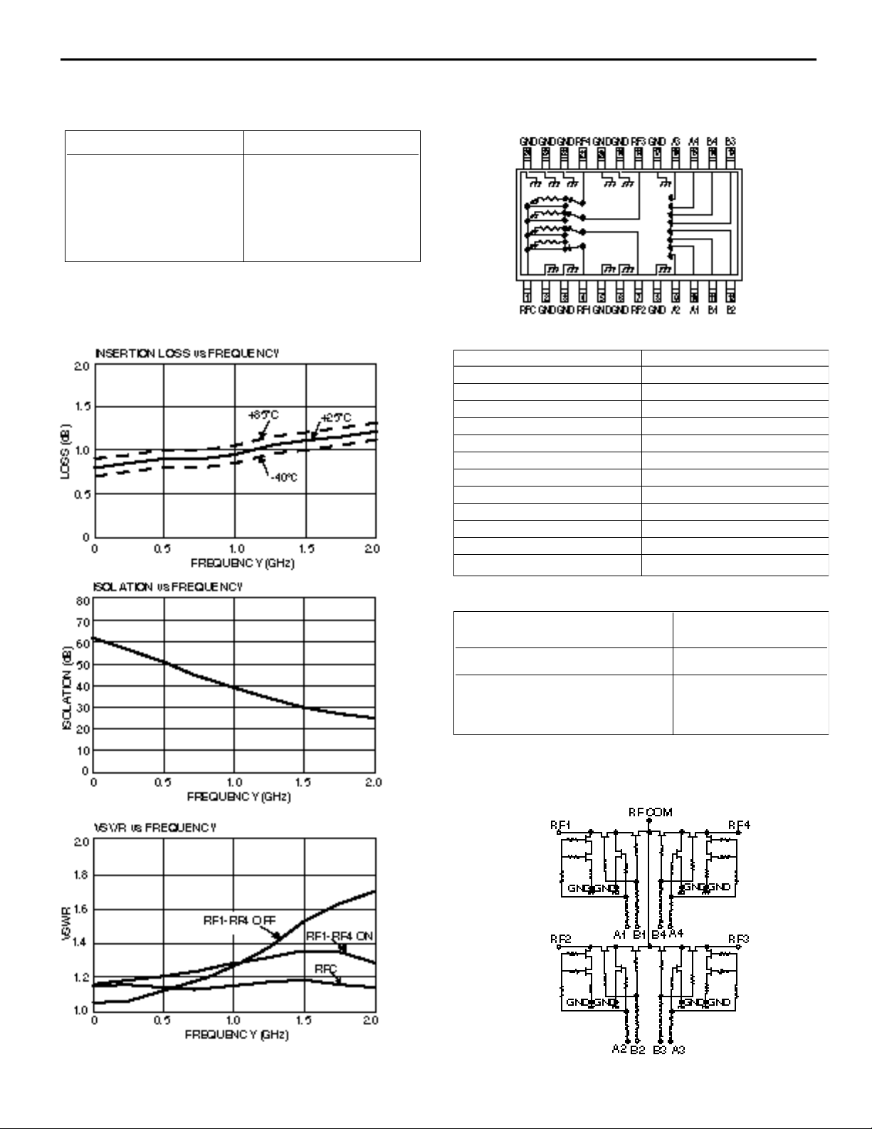
Pin Configuration
Truth Table
Electrical Schematic
GaAs SP4T Terminated Switch SW-419
Functional Schematic
V 2.00
Parameter Absolute Maximum
Max. Input Power
Below 500 MHz +27 dBm
A b ove 500 MHz +30 dBm
Control Voltage +5 V, – 8.5 V
Storage Temperature -65° to +150°C
Typical Performance
 Loading...