M A COM SVC6310 Datasheet

Specifications Subject to Change Without Notice.
M/A-COM Inc. 1
North America: Tel. (800) 366-2266 ♦ Asia/Pacific: Tel. +81 3 3263-8761 ♦ Europe: Tel. +44 (1344) 869-595
Fax (800) 618-8883 Fax +81 3 3263-8769 Fax +44 (1344) 300-020
GaAs Foundry Services
PROCESS PE3 PE3
V2.00
Features
• 0.5 µm MBE MESFET Technology for High Power
Applications
• MMICs up to 18 GHz
• 100 mm wafer diameter
• Layout and design assistance
• Space qualification
• Custom test and packaging
Description
M/A-COM’s PE3 process utilizes molecular beam epitaxy (MBE) to
implement a MESFET active layer structure that achieves high
efficiency and breakdown for multi-watt power applications thru
18GHz. The focus is on products for moderate to high volume
applications. M/A-COM offers a full compliment of foundry
services to meet the requirements for custom designing a MMICbased die or packaged product.
Typical RF Performance
FC06 (6X150) 900 um FET
Param. Test Conditions Freq. Typ. Val.
MAG VDS = 8V, IDS = .40I
DSS
2/12GHz 22/13.5dB
P
SAT
VDS = 8V, IDS = .40I
DSS
2/12GHz 680/525mW/mm
PAE VDS = 8V, IDS = .40I
DSS
2/12GHz 50/41%
ft VDS = 8V, IDS = .40I
DSS
------ 20GHz
Ordering Information
Part Number Description
FE43-0001 PE3 Wafer
SVC6310 Mask Set
Electrical Specifications: T
A
= +25 °°C
Parameter Test Conditions Units Min. Typ. Max.
200um PCM FET
IDSS VDS = 3V, VGS = 0V mA/mm 180 240 310
DC GM VDS = 3V, IDS = 0.5IDSS mS/mm 125 150 185
Vp VDS = 3V, IDS = 0.025IDSS V -1.2 -1.8 -2.2
BVgd IG = 0.1mA/mm V -11 -15 RF GM VDS = 3V, IDS = 0.5IDSS mS 25 32 45
Cgs VDS = 3V, IDS = 0.5IDSS pF .140 .200 .280
Cgd VDS = 3V, IDS = 0.5IDSS pF .015 .022 .028
Cds VDS = 3V, IDS = 0.5IDSS pF .025 .038 .050
Ft VDS = 3V, IDS = 0.5IDSS GHz 20 26 34
Sheet Resistances
NDRS (N- GaAs) l = 20mA Ohms/sq 340 375 410
NCRS (NiCr) l = 10mA Ohms/sq 42 50 58
GFRS (Gate Metal) l = 20mA Ohms/sq - .027 .040
MIM Capacitors
Capacitance/unit area f = 1MHz pF/mm
2
360 400 440
Capacitor Leakage V = 10V µA - - 0.5

GaAs Foundry Services Process PE3
V2.00
Specifications Subject to Change Without Notice.
2 M/A-COM Inc.
North America: Tel. (800) 366-2266 ♦ Asia/Pacific: Tel. +81 3 3263-8761 ♦ Europe: Tel. +44 (1344) 869-595
Fax (800) 618-8883 Fax +81 3 3263-8769 Fax +44 (1344) 300-020
Normalized Nominal Models
Parameter 25% I
DSS
8 V
DS
50% I
DSS
8 V
DS
IDS mA/mm 62.62 127.96
gm mS/mm 140.37 155.44
Cgs pF/mm 1.178 1.303
Cgd pF/mm 0.072 0.059
Cds pF/mm 0.172 0.185
Td pS 5.574 5.502
Ri Ohms-mm 2.093 1.729
Gds mS/mm 9.214 7.929
Ggs mS/mm 0.168 0.093
Rg Ohms/mm 47.996 47.996
Rs Ohms-mm 0.827 0.827
Rd Ohms-mm 0.865 0.865
Lg nH/Finger 0.108 0.108
Ld nH/Finger 0.108 0.108
Cgp pF/mm 0.148 0.148
Cdp pF/mm 0.148 0.148
Mask Layer Assignments
LAYER PROCESS
CODE
PROCESS
DESCRIPTION
3 OH Ohmic
4 BI Boron Isolation
5 RD Resistor Deposition
7 GF Gate Finger
8 GL Gate Interconnect
10 TV Top via
11 OL Overlay
12 AP Air-post
13 AS Air-Span
25 BV Back-via
28 FP Final Passivation
29 ST Saw Street
NOTE: U n u sed layer numbe rs a re res erve d fo r fu ture use.
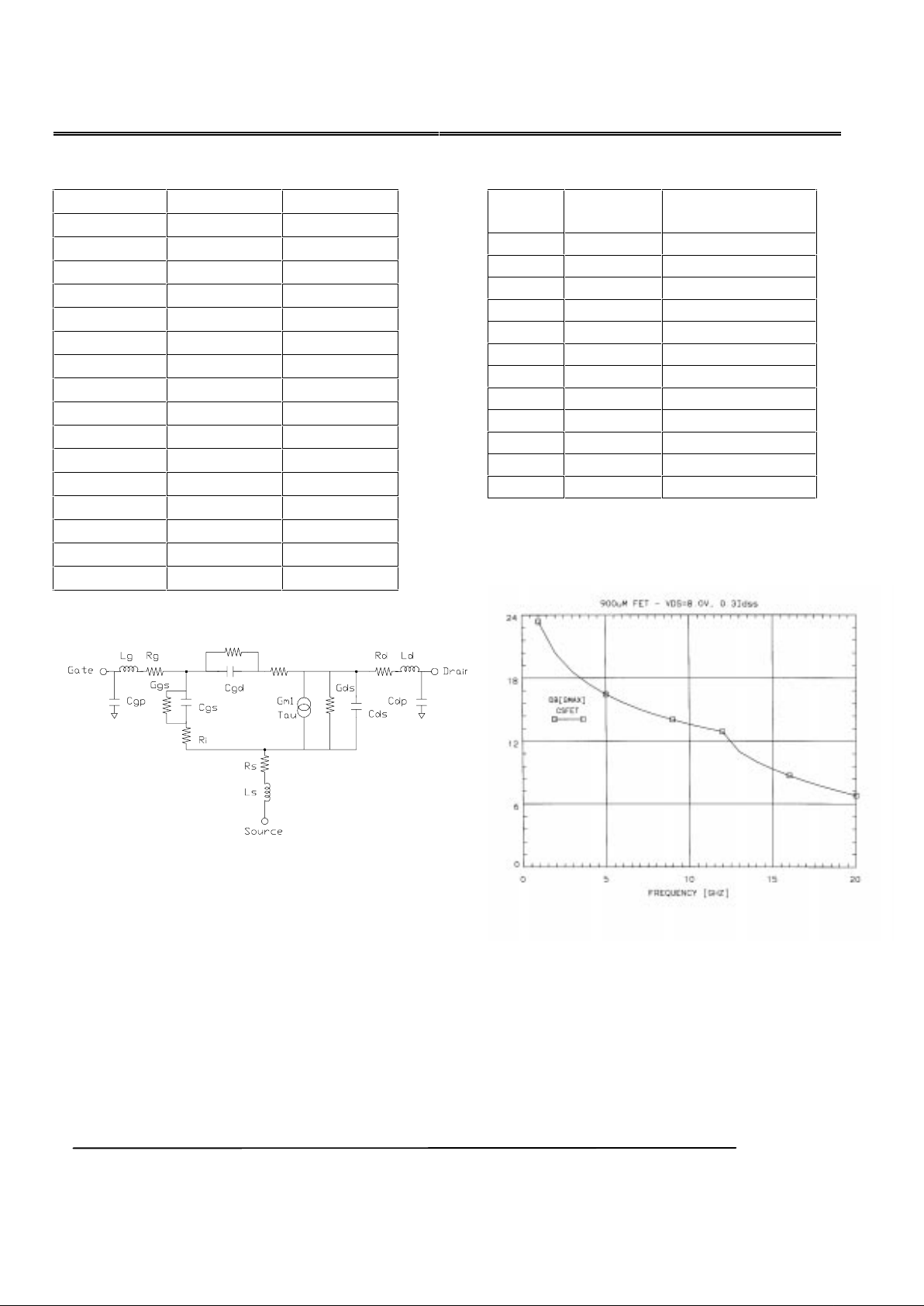
GMAX - 900um FET
 Loading...