M A COM MRF275G Datasheet
SEMICONDUCTOR TECHNICAL DATA
The RF MOSFET Line
Order this document
by MRF275G/D
Power Field-Effect Transistor
N–Channel Enhancement–Mode
Designed primarily for wideband large–signal output and driver stages from
100 – 500 MHz.
• Guaranteed Performance @ 500 MHz, 28 Vdc
Output Power — 150 Watts
Power Gain — 10 dB (Min)
Efficiency — 50% (Min)
100% Tested for Load Mismatch at all Phase Angles with VSWR 30:1
• Overall Lower Capacitance @ 28 V
C
— 135 pF
iss
C
— 140 pF
oss
C
— 17 pF
rss
• Simplified AVC, ALC and Modulation
Typical data for power amplifiers in industrial and
commercial applications:
• Typical Performance @ 400 MHz, 28 Vdc
Output Power — 150 Watts
Power Gain — 12.5 dB
Efficiency — 60%
• Typical Performance @ 225 MHz, 28 Vdc
Output Power — 200 Watts
Power Gain — 15 dB
Efficiency — 65%
G
G
D
(FLANGE)
D
MRF275G
150 W, 28 V, 500 MHz
N–CHANNEL MOS
BROADBAND
100 – 500 MHz
RF POWER FET
S
CASE 375–04, STYLE 2
MAXIMUM RATINGS
Rating Symbol Value Unit
Drain–Source Voltage V
Drain–Gate Voltage
(RGS = 1.0 MΩ)
Gate–Source Voltage V
Drain Current — Continuous I
Total Device Dissipation @ TC = 25°C
Derate above 25°C
Storage Temperature Range T
Operating Junction Temperature T
V
DSS
DGR
GS
D
P
D
stg
J
65 Vdc
65 Vdc
±40 Adc
26 Adc
400
2.27
–65 to +150 °C
200 °C
THERMAL CHARACTERISTICS
Characteristic Symbol Max Unit
Thermal Resistance, Junction to Case R
NOTE – CAUTION – MOS devices are susceptible to damage from electrostatic charge. Reasonable precautions in handling and
packaging MOS devices should be observed.
REV 1
θJC
0.44 °C/W
1
Watts
W/°C
ELECTRICAL CHARACTERISTICS (T
Characteristic
= 25°C unless otherwise noted)
C
OFF CHARACTERISTICS (1)
Drain–Source Breakdown Voltage
(VGS = 0, ID = 50 mA)
Zero Gate Voltage Drain Current
(VDS = 28 V, VGS = 0)
Gate–Source Leakage Current
(VGS = 20 V, VDS = 0)
ON CHARACTERISTICS (1)
Gate Threshold Voltage (VDS = 10 V, ID = 100 mA) V
Drain–Source On–Voltage (VGS = 10 V, ID = 5 A) V
Forward Transconductance (VDS = 10 V, ID = 2.5 A) g
DYNAMIC CHARACTERISTICS (1)
Input Capacitance (VDS = 28 V, VGS = 0, f = 1 MHz) C
Output Capacitance (VDS = 28 V, VGS = 0, f = 1 MHz) C
Reverse Transfer Capacitance (VDS = 28 V, VGS = 0, f = 1 MHz) C
FUNCTIONAL CHARACTERISTICS (2) (Figure 1)
Common Source Power Gain
(VDD = 28 V, P
Drain Efficiency
(VDD = 28 V, P
Electrical Ruggedness
(VDD = 28 V, P
VSWR 30:1 at all Phase Angles)
1. Each side of device measured separately.
2. Measured in push–pull configuration.
= 150 W, f = 500 MHz, IDQ = 2 x 100 mA)
out
= 150 W, f = 500 MHz, IDQ = 2 x 100 mA)
out
= 150 W, f = 500 MHz, IDQ = 2 x 100 mA,
out
Symbol Min Typ Max Unit
V
(BR)DSS
I
DSS
I
GSS
GS(th)
DS(on)
fs
iss
oss
rss
G
ps
η 50 55 — %
ψ
65 — — Vdc
— — 1 mA
— — 1 µA
1.5 2.5 4.5 Vdc
0.5 0.9 1.5 Vdc
3 3.75 — mhos
— 135 — pF
— 140 — pF
— 17 — pF
10 11.2 — dB
No Degradation in Output Power
REV 1
2
A
B
+V
GG
C14
B1
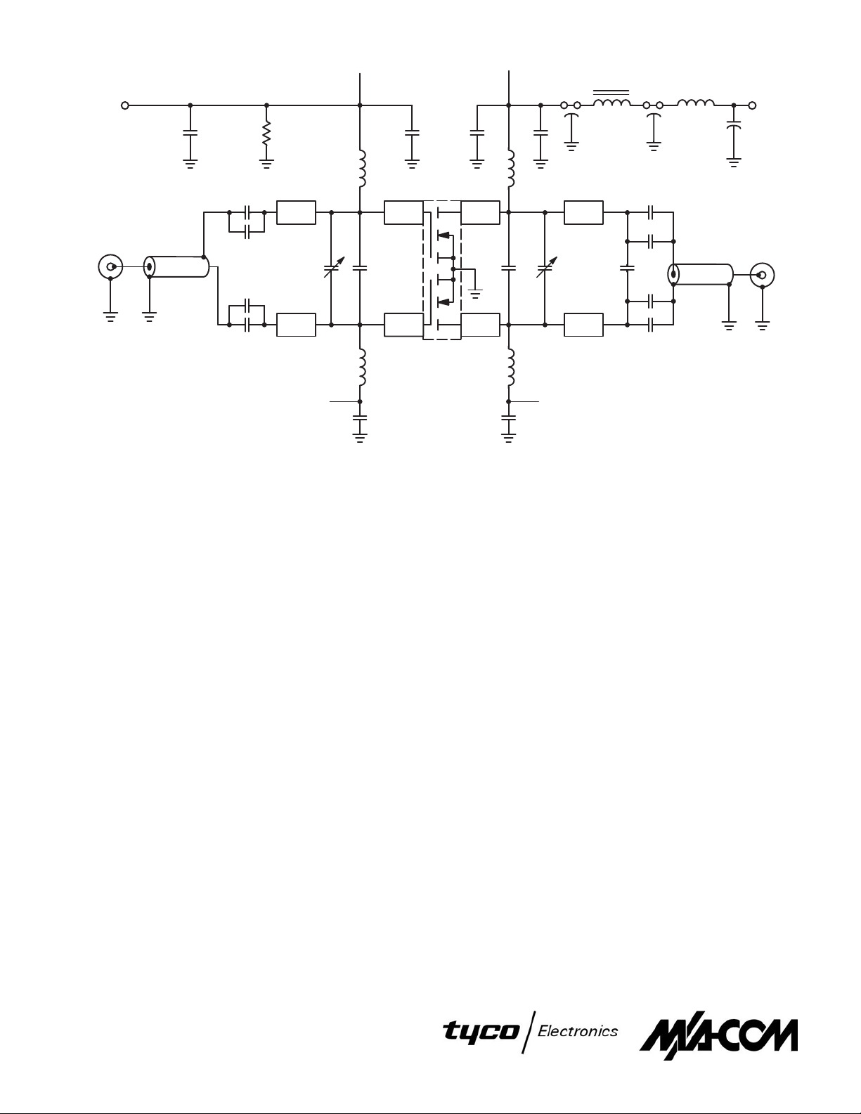
B1 Balun, 50 Ω, 0.086″ O.D. 2″ Long, Semi Rigid Coax
B2 Balun, 50 Ω, Coax 0.141″ O.D. 2″ Long, Semi Rigid
C1, C2, C3, C4,
C10, C11, C12, C13 270 pF, ATC Chip Capacitor
C5, C8 1.0–20 pF, Trimmer Capacitor, Johanson
C6 22 pF, Mini–Unelco Capacitor
C7 15 pF, Unelco Capacitor
C9 2.1 pF, ATC Chip Capacitor
C14, C15, C16,
C20, C21, C22 0.1 µF, Ceramic Capacitor
C17, C18 680 pF, Feedthru Capacitor
C19 10 µF, 50 V, Electrolytic Capacitor, Tantalum
L1, L2 10 Turns AWG #24,
L3, L4 10 Turns AWG #18,
R1
C1
Z1
C2
C5 C6 C7 C8
C3
Z2
C4
0.145″ O.D., 106 nH
T aylor–Spring Inductor
0.340″ I.D., Enameled Wire
C15
L1
Z3 Z7Z5
Z4
L2
C20 C21
C16
D.U.T.
Figure 1. 500 MHz T est Circuit
C11
C12
L6
C19
B2
+28 V
+
C17 C18
L5
C22
L3
C10
C9
Z8Z6
C13
L4
BA
L5 Ferroxcube VK200 20/4B
L6 4 Turns #16, 0.340″ I.D.,
Enameled Wire
R1 1.0 kΩ,1/4 W Resistor
W1 – W4 20 x 200 x 250 mils, Wear Pads,
Beryllium–Copper , (See
Component Location Diagram)
Z1, Z2 1.10″ x 0.245″, Microstrip Line
Z3, Z4, Z5, Z6 0.300″ x 0.245″, Microstrip Line
Z7, Z8 1.00″ x 0.245″, Microstrip Line
Board material 0.060″ Teflon–fiberglass,
εr = 2.55, copper clad both sides, 2 oz. copper.
Points A are connected together on PCB.
Points B are connected together on PCB.
REV 1
3
TYPICAL CHARACTERISTICS
300
250
200
150
100
, OUTPUT POWER (WATTS)
out
P
50
0
515
10
Pin, INPUT POWER (Watts)
225 MHz
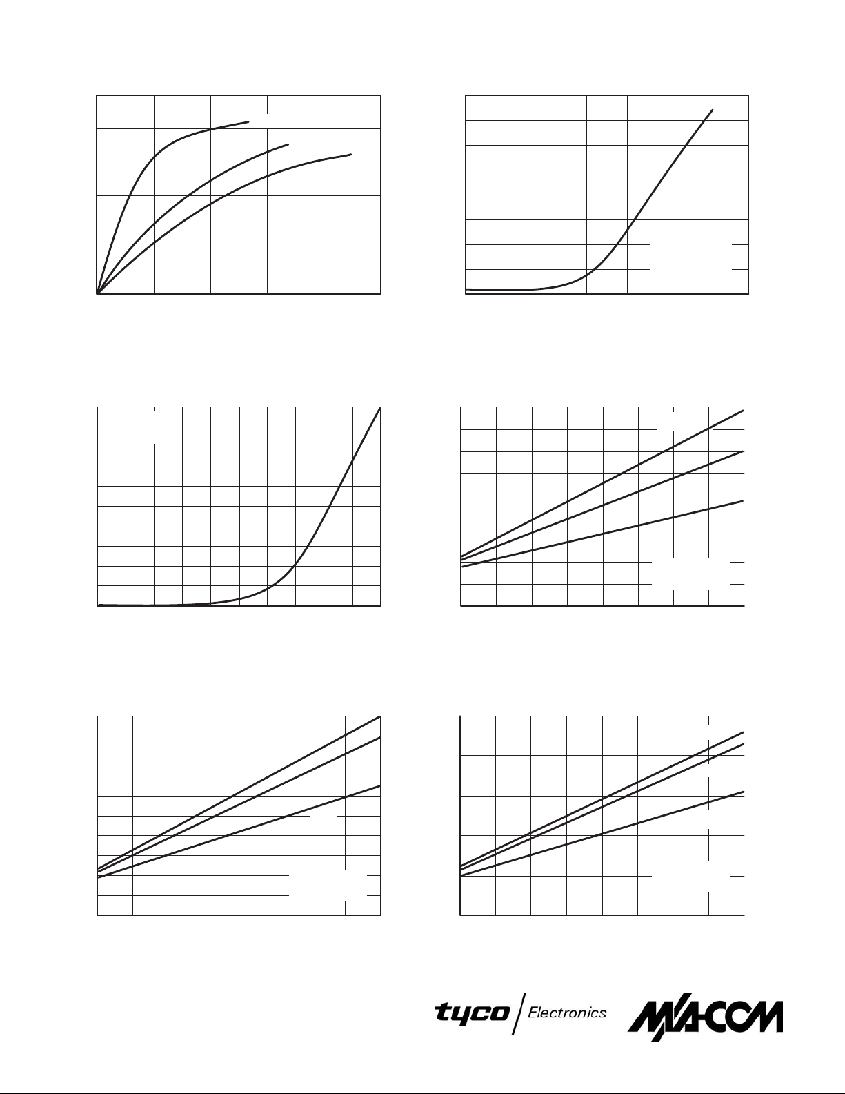
Figure 2. Output Power versus Input Power
10
VDS = 10 V
9
V
= 2.5 V
GS(th)
8
7
6
5
4
3
, DRAIN CURRENT (AMPS)
D
I
2
1
0
0
VGS, GATE–SOURCE VOLTAGE (V)
2
315
400 MHz
IDQ = 2 x 100 mA
VDD = 28 V
20
4
500 MHz
4.52.50.5 3.51.5
160
140
120
100
80
60
–2
VDS = 28 V
IDQ = 2 x 100 mA
Pin = Constant
f = 500 MHz
42
, OUTPUT POWER (WATTS)
40
out
P
20
0
25
–10 00
–8
–6 –4
VGS, GATE–SOURCE VOLTAGE (V)
Figure 3. Output Power versus Gate Voltage
180
Pin = 14 W
10 W
6 W
IDQ = 2 x 100 mA
f = 500 MHz
22 26
24
, OUTPUT POWER (WATTS)
out
P
160
140
120
100
80
60
40
20
0
14 1612
18 20 28
VDD, SUPPLY VOLTAGE (V)
Figure 4. Drain Current versus Gate Voltage
(Transfer Characteristics)
200
180
160
140
120
100
, OUTPUT POWER (WATTS)
out
P
80
60
40
20
0
14 1612 18 20 282422 26
VDD, SUPPLY VOLTAGE (V)
Pin = 14 W
IDQ = 2 x 100 mA
f = 400 MHz
Figure 6. Output Power versus Supply Voltage
REV 1
4
10 W
6 W
Figure 5. Output Power versus Supply Voltage
250
200
150
100
, OUTPUT POWER (WATTS)
out
P
50
0
14 1612 18 20 282422 26
VDD, SUPPLY VOLTAGE (V)
IDQ = 2 x 100 mA
f = 225 MHz
Figure 7. Output Power versus Supply Voltage
12 W
10 W
Pin = 4 W
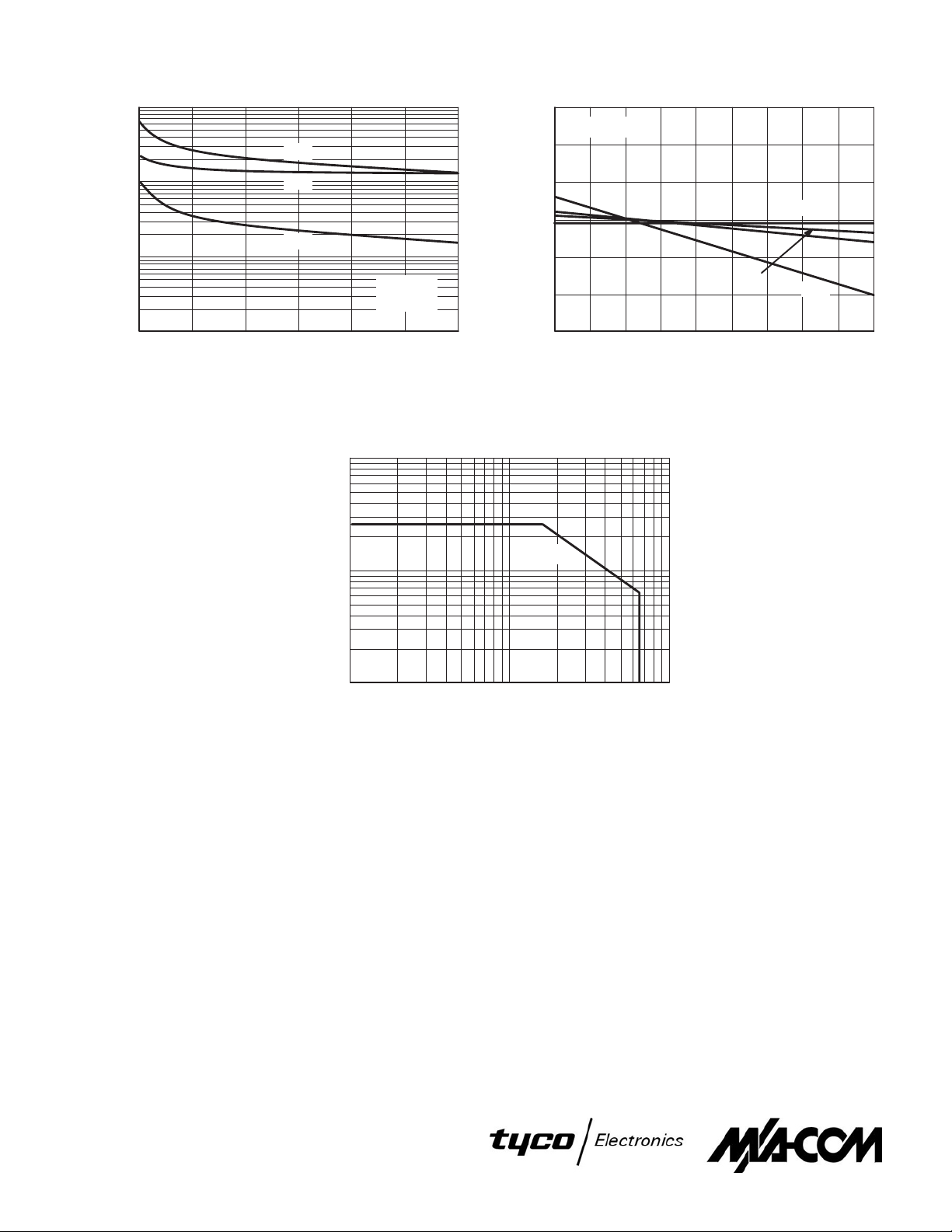
TYPICAL CHARACTERISTICS
1000
C
oss
C, CAPACITANCE (pF)
100
10
1
515
10
VDS, DRAIN–SOURCE VOLTAGE (V)
C
iss
C
rss
VGS = 0 V
f = 1.0 MHz
20
25
Figure 8. Capacitance versus Drain–Source V oltage*
*Data shown applies only to one half of
device, MRF275G
100
10
1.3
VDD = 28 V
1.2
1.1
1
0.9
0.8
, GATE–SOURCE VOLTAGE (NORMALIZED)
GS
V
0.7
30
–25 1750
25
500 100
75 125
TC, CASE TEMPERATURE (°C)
3 A
ID = 4 A
2 A
0.1 A
150
200
Figure 9. Gate–Source V oltage versus
Case T emperature
TC = 25°C
, DRAIN CURRENT (AMPS)
D
I
1
1 100
VDS, DRAIN–SOURCE VOLTAGE (V)
10
Figure 10. DC Safe Operating Area
REV 1
5
 Loading...