M A COM MRF166C Datasheet

SEMICONDUCTOR TECHNICAL DATA
The RF MOSFET Line
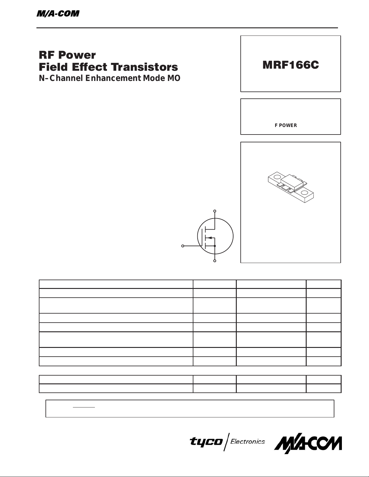
RF Power
Field Effect Transistors
N–Channel Enhancement Mode MOSFETs
Designed primarily for wideband large–signal output and driver from 30–500
MHz.
• MRF166C — Guaranteed Performance at 500 MHz, 28 Vdc
Output Power = 20 W
Gain = 13.5 dB
Efficiency = 50%
• Replacement for Industry Standards such as MRF136, DV2820, BLF244,
SD1902, and ST1001
• 100% Tested for Load Mismatch at all Phase Angles with 30:1 VSWR
• Facilitates Manual Gain Control, ALC and Modulation Techniques
• Excellent Thermal Stability , Ideally Suited for Class A Operation
• Low C
• Circuit board photomaster available upon request by
contacting RF Tactical Marketing in Phoenix, AZ.
— 4.0 pF @ VDS = 28 V
rss
Order this document
by MRF166C/D
MRF166C
20 W, 500 MHz
MOSFET
BROADBAND
RF POWER FETs
G
MAXIMUM RATINGS
Rating Symbol Value Unit
Drain–Gate Voltage V
Drain–Gate Voltage
(RGS = 1.0 MΩ)
Gate–Source Voltage V
Drain Current — Continuous I
Total Device Dissipation @ TC = 25°C
Derate Above 25°C
Storage Temperature Range T
Operating Junction Temperature T
THERMAL CHARACTERISTICS
Characteristic Symbol Max Unit
Thermal Resistance, Junction to Case R
V
D
DSS
DGR
GS
D
P
D
stg
J
θJC
CASE 319–07, STYLE 3
S
65 Vdc
65 Vdc
±20 Adc
4.0 Adc
70
0.4
–65 to 150 °C
200 °C
2.5 °C/W
Watts
W/°C
NOTE — CAUTION — MOS devices are susceptible to damage from electrostatic charge. Reasonable precautions in handling and
packaging MOS devices should be observed.
REV 10
1

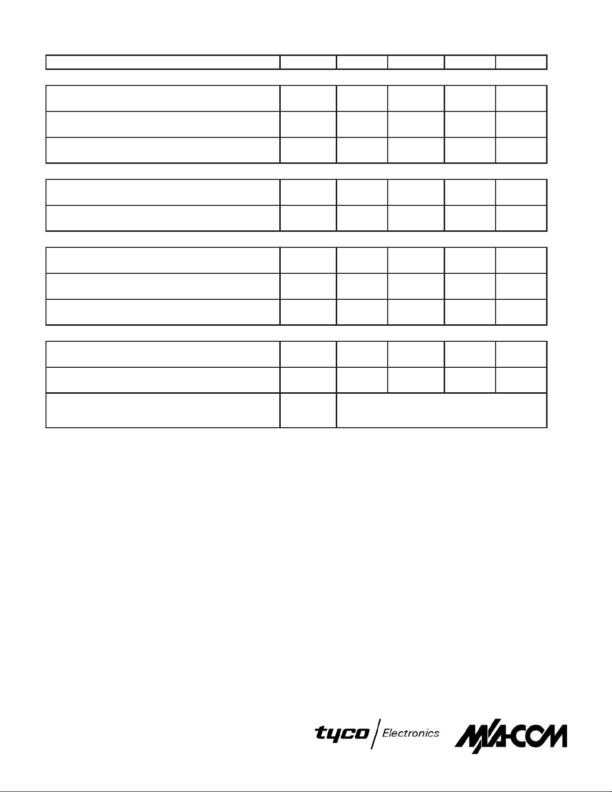
ELECTRICAL CHARACTERISTICS (T
Characteristic Symbol Min Typ Max Unit
OFF CHARACTERISTICS
Drain–Source Breakdown Voltage
(VGS = 0 V, ID = 5.0 mA)
Zero Gate Voltage Drain Current
(VDS = 28 V, VGS = 0 V)
Gate–Source Leakage Current
(VGS = 20 V, VDS = 0 V)
ON CHARACTERISTICS
Gate Threshold Voltage
(VDS = 10 V, ID = 25 mA)
Forward Transconductance
(VDS = 10 V, ID = 1.5 A)
DYNAMIC CHARACTERISTICS
Input Capacitance
(VDS = 28 V, VGS = 0 V, f = 1.0 MHz)
Output Capacitance
(VDS = 28 V, VGS = 0 V, f = 1.0 MHz)
Reverse Transfer Capacitance
(VDS = 28 V, VGS = 0 V, f = 1.0 MHz)
FUNCTIONAL CHARACTERISTICS
Common Source Power Gain
(VDD = 28 V, P
Drain Efficiency
(VDD = 28 V, P
Electrical Ruggedness
(VDD = 28 V, P
Load VSWR 30:1 at All Phase Angles)
= 20 W, f = 500 MHz, IDQ = 25 mA)
out
= 20 W, f = 500 MHz, IDQ = 25 mA)
out
= 20 W, f = 500 MHz, IDQ = 25 mA,
out
= 25°C unless otherwise noted)
C
V
(BR)DSS
I
DSS
I
GSS
V
GS(th)
g
C
C
oss
C
G
ψ No Degradation in Output Power
65 — — V
— — 0.5 mA
— — 1.0 µA
1.5 3.0 4.5 V
fs
iss
rss
ps
η 50 55 — %
0.8 1.1 — mhos
— 28 — pF
— 30 — pF
— 4.0 — pF
13.5 16 — dB
REV 10
2

RF
INPUT
Z3
BIAS
C1
R3
RFC1
C9
C8
R2
C4
RFC2
R1
Z1
C2
C3
DUT
Z2
C5
C10
C6
C7
VDD = 28 V
+
C11
–
OUTPUT
Z4
+
Vdc
–
RF
C1, C7 200 pF, Chip Capacitor
C2, C6 2–10 pF, Trimmer Capacitor, Johansen
C3 27 pF, ATC 100 mil Chip Capacitor
C4, C8 0.1 µF, Chip Capacitor
C5 15 pF, ATC 100 mil Chip Capacitor
C9, C10 680 pF, Feedthru Capacitor
C11 50 µF, 50 V, Electrolytic Capacitor
R1 120 Ω, 1/2 W Resistor
R2 10 kΩ, 1/2 W Resistor
R3 1 kΩ, 1/2 W Resistor
RFC1 Ferroxcube VK200 19/4B
RFC2 10 Turns AWG #18, 0.125″I.D., Enameled
Board Material 0.062″ Teflon Fiberglass
1 oz. Copper Clad Both Sides
εr = 2.56
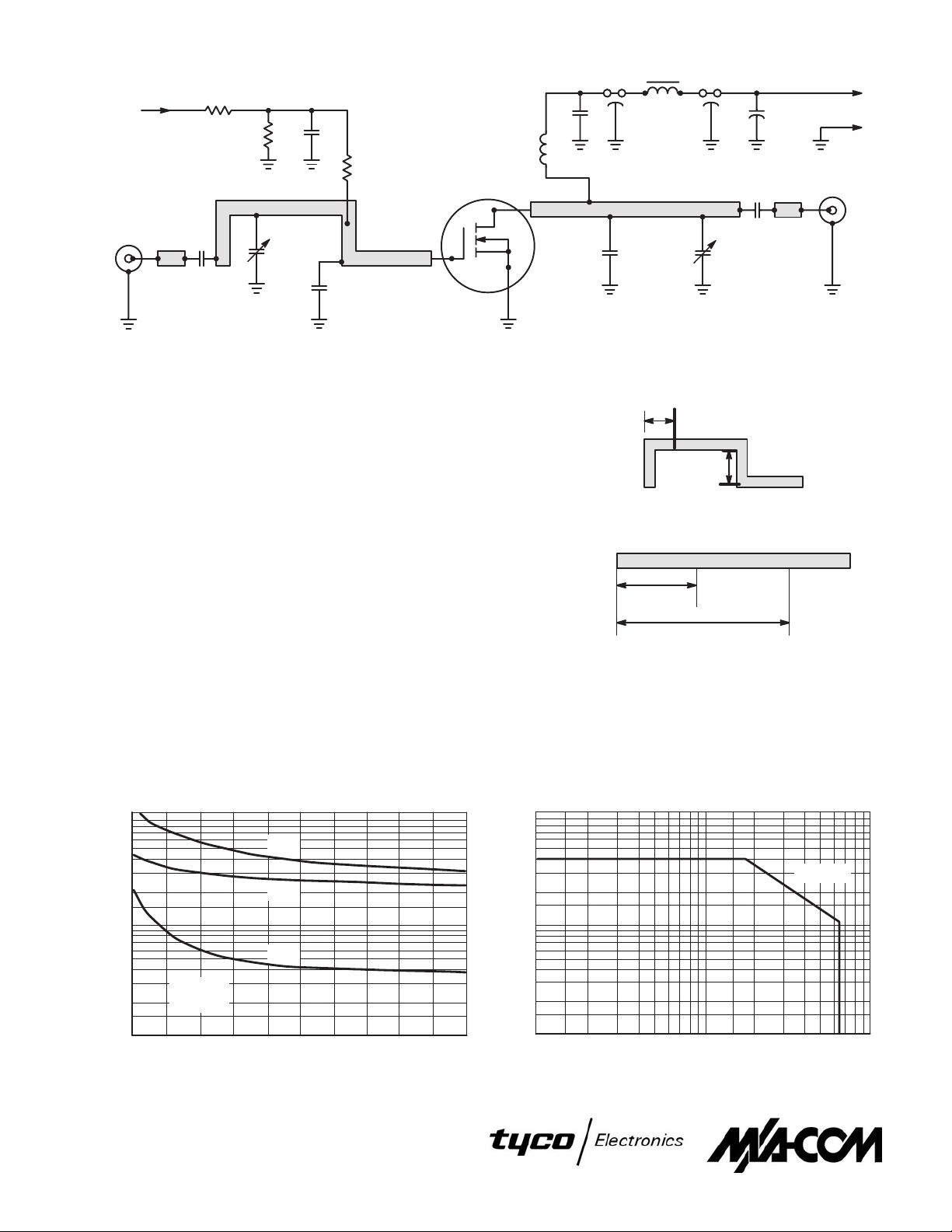
Figure 1. MRF166C 500 MHz T est Circuit
TYPICAL CHARACTERISTICS
100
Z1 0.120″ x 3.3″, Microstrip Line
350 mils
C2
600 mils
C3
Z2 0.120″ x 2.1″, Microstrip Line
C5 C6
825 mils
1650 mils
Z3, Z4 0.120″ x 0.25″, Microstrip Line
10
C
oss
C
iss
C
rss
C, CAPACITANCE (pF)
50
20
10
5
2
1
VGS = 0 V
f = 1 MHz
VDS, DRAIN–SOURCE VOLTAGE (VOLTS)
Figure 2. Capacitance versus Drain–Source V oltage
REV 10
3
TC = 25°C
1
, DRAIN CURRENT (AMPS)
D
I
2520151050
0.1
VDS, DRAIN–SOURCE VOLTAGE (VOLTS)
100100
Figure 3. DC Safe Operating Area
 Loading...