M A COM MLS9204-01745TR, MLS9204-01745 Datasheet

Surface Mount Frequency Synthesizer MLS9204-01745
M/A-COM Division of AMP Incorporated ■ North America: Tel. (800) 366-2266, Fax (800) 618-8883 ■ Asia/Pacific: Tel.+85 2 2111 8088,
Fax +85 2 2111 8087
■
Europe: Tel. +44 (1344) 869 595, Fax+44 (1344) 300 020
www.macom.com
AMP and Connecting at a Higher Level are trademark s.
Specifications subject to change without notice.
V2.00
Parameter Test Conditions Units Min. Typ. Max.
Frequency Range (F
OUT
)
2
Over T
OP
MHz 1710 —- 1780
RF Output Power (P
OUT
)
3
Over T
OP
dBm -3.0 —- +3.0
Harmonic Output dBc —- -19 -10
Spurious Output
Phase comparison fr equency (F
OUT
± ∆F)
dBc —- -80 -60
Reference breakthr ough (F
OUT±FR
) dBc —- -85 —-
Phase Noise
4
SSB at 1 kHz offset fr om carrier dBc/Hz —- -70 - 65
SSB at 10 kHz offset fr om carrier dBc/Hz —- -98 - 90
SSB at 100 kHz offset fr om carrier dBc/Hz —- -118 -110
SSB at 1.25 MHz offset from c arrier dBc/Hz —- -139 —Integrated Phase Noise 300 Hz to 3 kHz bandwidth mrad rms —- 30 —Frequency Switching Time
5,6
Over F
OUT
, measured to within ±500 Hz ms —- 35 —-
VCO Supply Current (I
CC1
)mA—-1720
PLL Supply Current (I
CC2
)mA—-1015
VCO Supply Voltage (V
CC1
) Recommended operating limit V +4.75 —- +5.25
PLL Supply Voltage (V
CC2
) Recommended operating limit V +4.75 —- +5.25
Step Size (∆F)
7
Recommended operating limit kHz —- 50 —Reference Frequency (F
R
)
8
0.5 to 2.0 Vpp sine wave into a. c. coupled
CMOS. Recommended operating limit
MHz 3 —- 20
Features
•
Integrated VCO/PLL
•
Miniature SMT Package
•
Low Phase Noise
•
+5V Operation
Description
The MLS9204-01745 synthesizer design integrates a high performance buffered VCO, PLL circuit and discrete loop filter in a
surface mount package. The SMT packaging provides electrical
shielding, easy PCB assembly and repeatable performance. The
synthesizer is designed for use in PCS CDMA base stations and is
optimised for coverage of the PCS Rx band with 50 kHz step size
and low phase noise.
M/A-COM synthesizers are manufactured in an ISO 9001 certified facility, incorporating surface mount assembly and automated
electrical testing. This ensures consistent electrical performance
and quality over volume production quantities.
Electrical Specifications1, TA = +25°C, VCC = +5V, ∆∆F = 50 kHz, FR = 15 MHz
(unless otherwise stated)
1. All specification limits ar e indicated values and apply over F
OUT
and
for 50Ω load impedance.
2. Programming control is 3 wire serial CMOS or TTL level s, in accordance with National Semiconductor LMX 2325.
3. Output power window includes variation over operating temperature
range (T
OP
) -40°C to +85°C and output frequency range (F
OUT
).
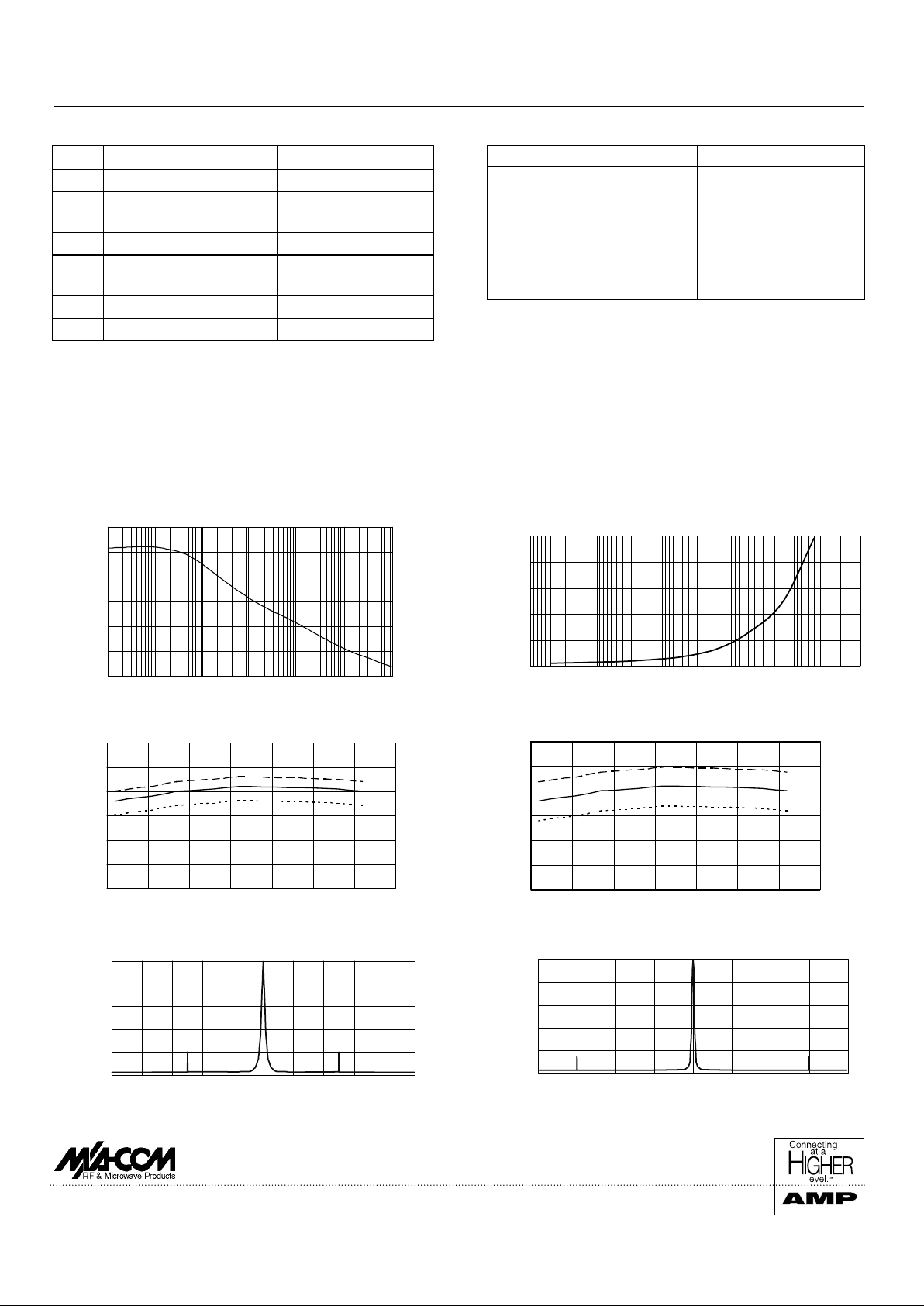
4. See plot for typical phase noise at other frequency offsets.
Surface Mount Frequency Synthesizer
CDMA 1710 - 1780 MHz
MLS9204-01745
5. See plot for typical f ull band switching time measured to within
other offsets from final frequency.
6. Integral PLL lock monitor output, TTL high locked, TTL low unlocked.
7. Device designed for loop bandwidth of 225 Hz.
8. Reference frequency input impedance 10kΩ min.
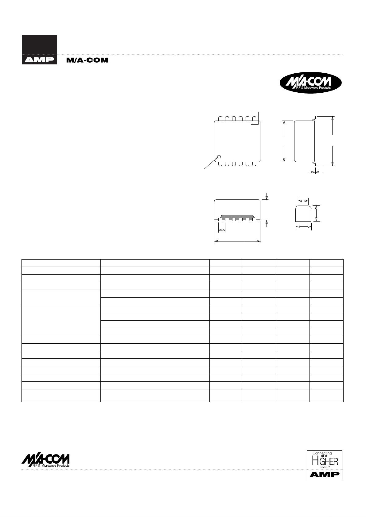
12 Lead Package
1.0
13.2
6.0 MAX
12.0
14.6
0.2
2.0
TYP.in 5 POSITIONS
781112 10 9
64321
DATE CODE
PART NO.
M/ A- COM LTD
IDENT
DETAIL A
0.6
0.8
5
DETAIL A

Surface Mount Frequency Synthesizer MLS9204-01745
M/A-COM Division of AMP Incorporated ■ North America: Tel. (800) 366-2266, Fax (800) 618-8883 ■ Asia/Pacific: Tel.+85 2 2111 8088,
Fax +85 2 2111 8087
■
Europe: Tel. +44 (1344) 869 595, Fax+44 (1344) 300 020
www.macom.com
AMP and Connecting at a Higher Level are trademark s.
Specifications subject to change without notice.
V2.00
Reference Breakthrough Spurious
Phase Noise
4.75 V
5.00 V
5.25 V
Absolute Maximum Ratings
1,2
Parameter Absolute Maximum
VCO Supply Volta
g
e (V
CC1
)
3
+6.5V
PLL Supply Volta
g
e (V
CC2
)
3
+6.5V
Reference Frequency Volta
g
e -0.3V to +6.5V
Data, Clock, Strobe Volta
g
es -0.3V to +6.5V
Stora
g
e Temperature (T
STOR
) -45°C to +125°C
Solder Assembly Temperature See App Note M2032
1. Exceeding these limits may cause permanent damage.
2. Static sensitive, observe appropriate handling precautions.
3. An external series resistor and bypass capacitor will allow operation at higher supply voltage and will improve power supply decoupling and noise suppression.
Environmental Specifications
Devices are designed to function over the operating temperature
range (T
OP
) of -40°C to +85°C and after exposure to the shock,
vibration, thermal shock and moisture conditions typically encountered in base station and other infrastructure environments.
Functional Configuration
Lead Function Lead Function
1 Ground 7 Ground
2 Clock Input 8 Reference
Frequency Input
3V
CC1
(VCO) 9 V
CC2
(PLL)
4 PLL Lock
Monitor Output
10 Data Input
5 RF Output 11 Strobe/Enable Input
6 Ground 12 Ground
Phase Comparator Spurious
Typical Performance
Ordering Information
Synthesizers are available in either tape and reel or tube packaging.
To order devices in tape and reel requires the suffix TR to be
added to the part number, i.e. MLS9204-01745TR. Quantity 500
per 13 inch reel, see Application Note M2030.
Full Band Switching Time
Output Power vs Temperature
Output Power vs Supply Voltage
+25 °C
-40 °C
+85 °C
PHASE NOISE (dBc/Hz)
FREQUENCY OFFSET FROM CARRIER (Hz)
-40
-60
-80
-100
-120
-140
-160
10 100 1K 10K 100K 1M 10M
TIME (ms)
OFFSET FROM FINAL FREQUENCY (Hz)
500
400
300
200
100
0
100K 10K 1K 100 10 1
OUTPUT POWER (dBm)
FREQUENCY (MHz)
3.0
2.0
1.0
0.0
-1.0
-2.0
-3.0
1680 1700 1720 1740 1760 1780 1800 1820
OUTPUT POWER (dBm)
FREQUENCY (MHz)
3.0
2.0
1.0
0.0
-1.0
-2.0
-3.0
SPURIOUS LEVEL (dBc)
FREQUENCY OFFSET FROM CARRIER (kHz)
0
-20
-40
-60
-80
-100
-100 -80 -60 -40 -20 0 20 40 60 80 100
SPURIOUS LEVEL (dBc)
FREQUENCY OFFSET FROM CARRIER (MHz)
0
-20
-40
-60
-80
-100
-20 -15 -10 -5 0 5 10 15 20
1680 1700 1720 1740 1760 1780 1800 1820
 Loading...