M A COM MLO81100-01960 Datasheet

Surface Mount Voltage Controlled Oscillator MLO81100-01960
g
g
g
g
g
g
g
MLO81100-01960
Surface Mount Voltage Controlled Oscillator
PCS 1930 - 1990 MHz
Features
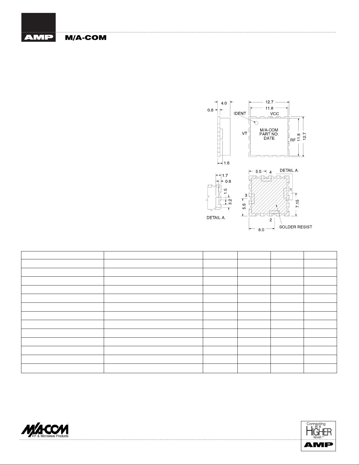
LSM1 Package
• Miniature Size
• Surface Mount Package
• Electrically Shielded
• Low Phase Noise
• Highly Linear Tuning
Description
The MLO81100-01960 is a fundamental single ended oscillator
designed for use in cost sensitive wireless and telemetry applications. The device has been optimized by careful selection of the
bipolar transistor and varactor diode for low phase noise and high
linearity tuning characteristics.
The low profile surface mount package used provides for
electrical shielding, ease of assembly and repeatable performance. M/A-COM’s surface mount manufacturing techniques together with automatic assembly and electrical
testing ensure a high degree of electrical and mechanical
repeatability at low cost and in high volume. Manufacturing
is carried out in an ISO 9000 qualified facility.
Electrical Specifications1, TA = +25°C, VCC = +5V
Parameter Test Conditions Units Min. Typ. Max.
Frequency Ran
Tunin
Voltage (VT)
RF Output Power
Supply Volta
Supply Current (I
Phase Noise
Avera
e Tuning Sensitivity
Tunin
Linearity 1930 - 1990 MHz Ratio — 1.2 2.0
Harmonic Outputs
Frequency Pushin
Frequency Pullin
Frequency Drift -20°C to +70°C MHz/°C — -0.16 —
Tune Input Capacitance — pF — — 50
1. All specifications apply with a 50 ohm load impedance.
2. Tuning voltages shown are the minimum and maximum voltages
required to tune the frequency range including temperature effects 20°C to +70°C. Devices will oscillate normally with tuning voltages
from 0V to +10V.
3. Output power window includes unit to unit variation, temperature
effects -20°C t o +70°C and frequency flatness (typically 0.5 dB at
any constant temperat ure).
e — MHz 1930 — 1990
2
3
4
e (VCC)
)—mA—1315
CC
5
6
7
1930 - 1990 MHz dBm -3.0 — +3.0
SSB at 100 kHz offset from carrier dBc/Hz — -118 -115
1930 - 1990 MHz MHz/V — 31 —
— V +0.5 — +4.5
— V +4.75 +5.00 +5.25
—dBc—-22-15
VCC 4.75V to 5.25V MHz/V — 1.7 3.0
1.5:1 VSWR load, all phases MHz — 4.5 5.5
(unless otherwise stated)
4. Devices may be operated at lower typical supply vol tage with
reduced performance.
5. For typical phase noise at other offsets see phase noise curve.
6. Defined as (1990-1930) / (V
7. Non harmonic spurious less than -70dBc.
1990 - VT 1930) MHz/V.
T
V4.00
www.macom.com
M/A-COM Division of AMP Incorporated ■ North America: Tel. (800) 366-2266, Fax (800) 618-8883 ■ Asia/Pacific: Tel.+85 2 2111 8088,
Fax +85 2 2111 8087
AMP and Connecting at a Higher Level are trademark s.
Specifications subject to change without notice.
■
Europe: Tel. +44 (1344) 869 595, Fax+ 44 (1344) 300 020

Surface Mount Voltage Controlled Oscillator MLO81100-01960
m
g
g
g
z
z
Absolute Maximum Ratings
1
Parameter Absolute Maximum
Tunin
Voltage (VT) 0 to +15V
Supply Volta
Stora
e2 (V
e Temperature -45°C to +100°C
)+6V
CC
Solder Assembly Temperature +230°C for 10 secs
1. Exceeding these limits may cause permanent damage.
2. A series resist or will allow operation at any greater supply voltage.
Used in conjunction with a bypass capacitor this will yield improved
power supply decoupling and noise suppression.
3. Static sensi tive, observe appropri ate precautions.
Environmental Specifications
Devices are designed to operate over the temperature range of
-20°C to +70°C and after exposure to the shock, vibration, thermal
shock and moisture conditions typically encountered in base station and subscriber terminal environments.
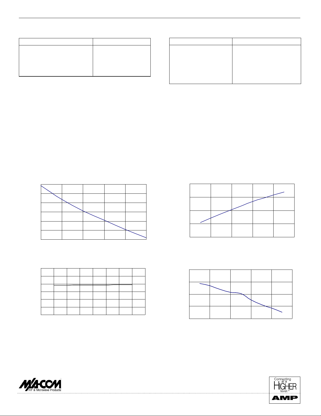
Typical Performance
Phase Noise
-40
@ +25°C and V
CC
+5V
Functional Configuration
Pad Configuration
1 RF Output
2V
3V
4 N/C or Ground
Case / Lid Ground
Substrate Material FR4.
Tuning Curve
2.05
CC
T
-60
-80
-100
-120
-140
PHASE NOISE (dBc/H
PHASE NOISE (dBc/Hz)
-160
100 1k 10k 100k 1M 10M
FREQUENCY OFFSET FROM CARRIER (Hz)
FREQUENCY OFFSET FROM CARRIER (Hz)
Output Power
3.0
2.0
1.0
0.0
-1.0
-2.0
OUTPUT POWER (dB
-3.0
OUTPUT POWER (dBm)
1.92 1.93 1.94 1.95 1.96 1.97 1.98 1.99 2.00
FREQUENCY (GHz)
FREQUENCY (GHz)
2.00
1.95
1.90
FREQUENCY (GH
FREQUENCY (GHz)
1.85
0.0 1.0 2.0 3.0 4.0 5.0
TUNING VOLTAGE (V)
TUNING VOLTAGE (V)
Tuning Sensitivity
40.0
35.0
30.0
25.0
20.0
TUNING SENSITIVITY (MHz/V)
0.0 1.0 2.0 3.0 4.0 5.0
TUNING VOLTAGE (V)
TUNING VOLTAGE (V)
www.macom.com
M/A-COM Division of AMP Incorporated ■ North America: Tel. (800) 366-2266, Fax (800) 618-8883 ■ Asia/Pacific: Tel.+85 2 2111 8088,
Fax +85 2 2111 8087
AMP and Connecting at a Higher Level are trademark s.
Specifications subject to change without notice.
■
Europe: Tel. +44 (1344) 869 595, Fax+ 44 (1344) 300 020
V4.00
 Loading...