M A COM MLO81100-01850 Datasheet

Surface Mount Voltage Controlled Oscillator
DCS 1800 - 1900 MHz
MLO81100-01850
V3.00
M/A-COM Ltd.
North America: Tel. (800) 366-2266 ■ Asia/Pacific: Tel. +85 2 2375 0618 ■ Europe: Tel. +44 (1344) 869 595
Fax (800) 618-8883 Fax +85 2 2375 0350 Fax +44 (1344) 300 020
1
Specifications Subject to Change Without Notice.
Parameter Test Conditions Units Min. Typ. Max.
Frequency Range MHz 1800 1900
Tuning Voltage (VT)
2
V +0.5 +4.5
RF Output Power
3
1800 - 1900 MHz dBm -3.0 +3.0
Supply Voltage (VCC)
4
V +4.75 +5.00 +5.25
Supply Current (ICC)mA1315
Phase Noise
5
SSB at 100 kHz offset from carrier dBc/Hz -118 -114
Average Tuning Sensitivity
6
1800 - 1900 MHz MHz/V 50
Tuning Linearity 1800 - 1900 MHz Ratio 1.5 2.0
Harmonic Outputs
7
dBc -22 -15
Frequency Pushing VCC4.75V to 5.25V MHz/V 1.5 2.5
Frequency Pulling 1.5:1 VSWR load, all phases MHz 4.5 5.5
Frequency Drift -20°C to +70°C MHz/°C -0.15
Tune Input Capacitance pF 50
Electrical Specifications1, T
A
= +25°C, VCC= +5V (unless otherwise stated)
Features
Miniature Size
Surface Mount Package
Electrically Shielded
Low Phase Noise
Highly Linear Tuning
Description
The MLO81100-01850 is a fundamental single ended
oscillator designed for use in cost sensitive wireless and
telemetry applications. The device has been optimised by
careful selection of the bipolar transistor and varactor diode
for low phase noise and high linearity tuning characteristics.
The low profile surface mount package used provides for
electrical shielding, ease of assembly and repeatable
performance. M/A-COM’s surface mount manufacturing
techniques together with automatic assembly and electrical
testing ensure a high degree of electrical and mechanical
repeatability at low cost and in high volume. Manufacturing
is carried out in an ISO 9000 qualified facility.
●
●
●
●
●
1. All specifications apply with a 50 ohm load impedance.
2. Tuning voltages shown are the minimum and maximum voltages
required to tune the frequency range including temperature effects
-20°C to +70°C. Devices will oscillate normally with tuning voltages
from 0V to +10V.
3. Output power window includes unit to unit variation, temperature
effects -20°C to +70°C and frequency flatness (typically 0.5 dB at
any constant temperature).
4. Devices may be operated at lower typical supply voltage with
reduced performance.
5. For typical phase noise at other offsets see phase noise curve.
6. Defined as (1900 - 1800) / (VT1900 - VT1800) MHz/V.
7. Non harmonic spurious less than -70dBc.
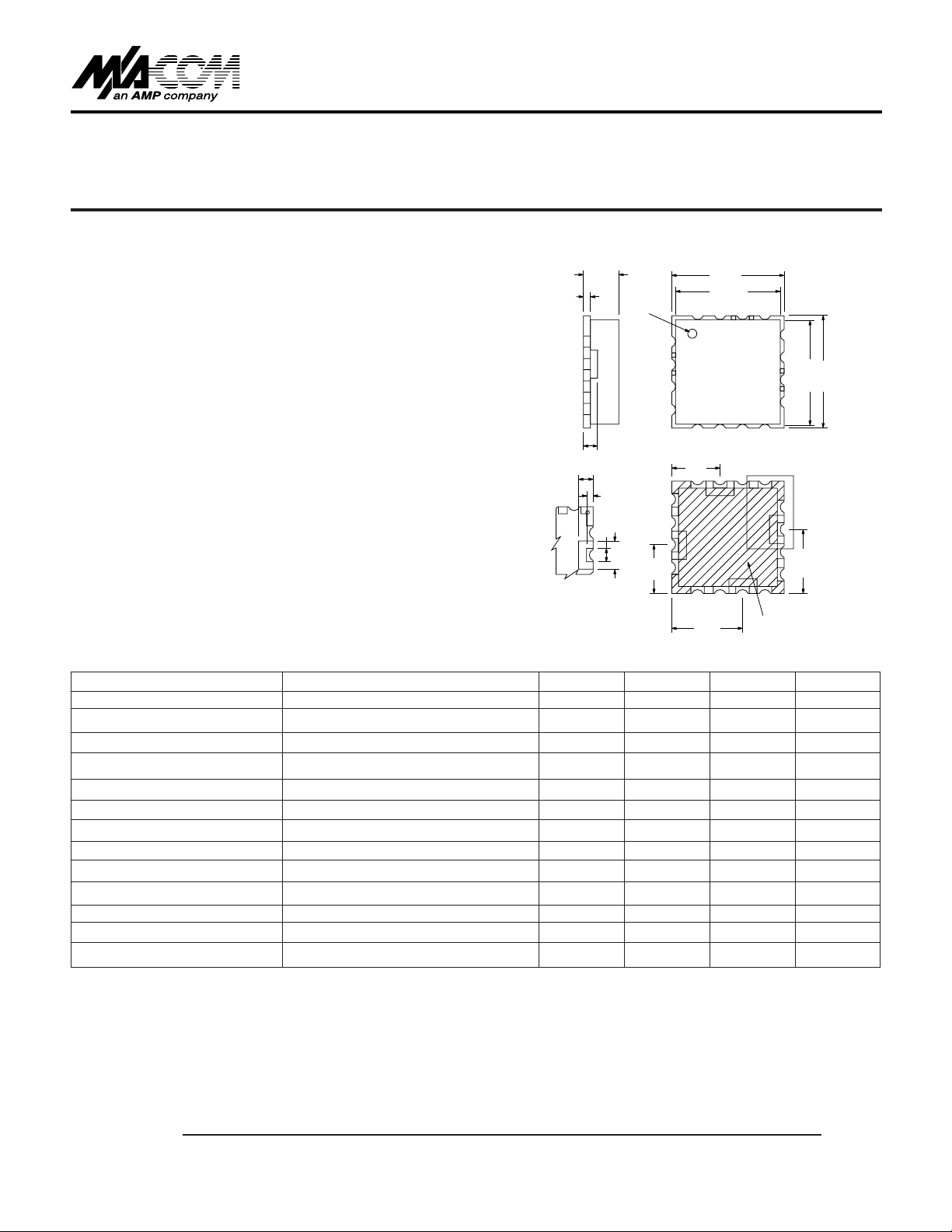
LSM1 Packa ge
0.8
4.0
IDENT
12.7
11.8
VCC
M/A-COM
PART NO.
DATE
VT
RF
11.8
3.2
7.15
5.5
1.5
12.7
1.6
1.7
0.8
3
5.5
4
DETAIL A.
DETAIL A.
1
2
SOLDER RESIST
8.0

Surface Mount Voltage Controlled Oscillator MLO81100-01850
V3.00
M/A-COM Ltd.
North America: Tel. (800) 366-2266 ■ Asia/Pacific: Tel. +85 2 2375 0618 ■ Europe: Tel. +44 (1344) 869 595
Fax (800) 618-8883 Fax +85 2 2375 0350 Fax +44 (1344) 300 020
2
Specifications Subject to Change Without Notice.
Envir onmental Specifications
Devices are designed to operate over the temperature range
of -20°C to +70°C and after exposure to the shock,
vibration, thermal shock and moisture conditions typically
encountered in base station and subscriber terminal
environments.
Substrate Material FR4.
Parameter Absolute Maximum
Tuning Voltage (V
T
) 0 to +15V
Supply Voltage
2
(VCC) +6V
Storage Temperature -45°C to +100°C
Solder Assembly Temperature +230°C for 10 secs
Absolute Maximum Ratings
1
Pad Configuration
1 RF Output
2 V
CC
3 V
T
4 N/C or Ground
Case / Lid Ground
Functional Configuration
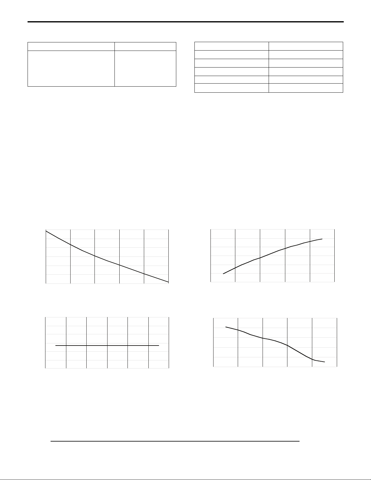
T ypical Performance @ +25°C and V
CC
+5V
OUTPUT POWER
TUNING CURVE
PHASE NOISE
TUNING SENSITIVITY
FREQUENCY (GHz)
OUTPUT POWER (dBm)
3.0
2.0
1.0
0.0
-1.0
-2.0
-3.0
1.79 1.81 1.83 1.85 1.87 1.89 1.91
FREQUENCY OFFSET FROM CARRIER (Hz)
PHASE NOISE (dBc/Hz)
-40
-60
-80
-100
-120
-140
-160
100 1K 10K 100K 1M 10M
TUNING VOLTAGE (V)
TUNING
SENSITIVITY (MHz/V)
75.0
65.0
55.0
45.0
35.0
25.0
0.0 1.0 2.0 3.0 4.0 5.0
TUNING VOLTAGE (V)
FREQUENCY (GHz)
2.00
1.95
1.90
1.85
1.80
1.75
1.70
0.0 1.0 2.0 3.0 4.0 5.0
1. Exceeding these limits may cause permanent damage.
2. A series resistor will allow operation at any greater supply voltage.
Used in conjunction with a bypass capacitor this will yield
improved power supply decoupling and noise suppression.
3. Static sensitive, observe appropriate precautions.
 Loading...