M A COM MD59-0021TR, MD59-0021RTR Datasheet

(1)
PCS CDMA LNA / Downconverter
PCS CDMA LNA / Downconverter
PCS CDMA LNA / DownconverterPCS CDMA LNA / Downconverter
1.8
1.8————2.0 GHz
1.81.8
2.0 GHz
2.0 GHz2.0 GHz
MD59-0021
Features
• High Integrated LNA and Downconverter
• Operates over 2.7 V to 5V Supply Voltage
• Low Noise Figure < 2.7 dB
• High Input Intercept Point -12 dBm
• Optional Control of LNA IP
3
• Low LO Drive Level -10 dBm
• Operates in US and Korean PCS Bands
• Miniature TSSOP-16 Plastic Package
Description
M/A-COM’s MD59-0021 is a fully integrated downconverter IC
with LNA, RF amplifier, downconverting mixer, IF amplifier
and LO buffer amplifier in a miniature TSSOP-16 plastic
package with exposed metal lead frame backside for improved
high frequency grounding.
The MD59-0021 is ideally suited for CDMA handset
applications where wide dynamic range and low power
consumption are important receiver requirements.
The MD59-0021 is fabricated using a M/A-COM’s 0.5 micron
low noise E/D GaAs MESFET process. The process features
full passivation for increased performance and reliability.
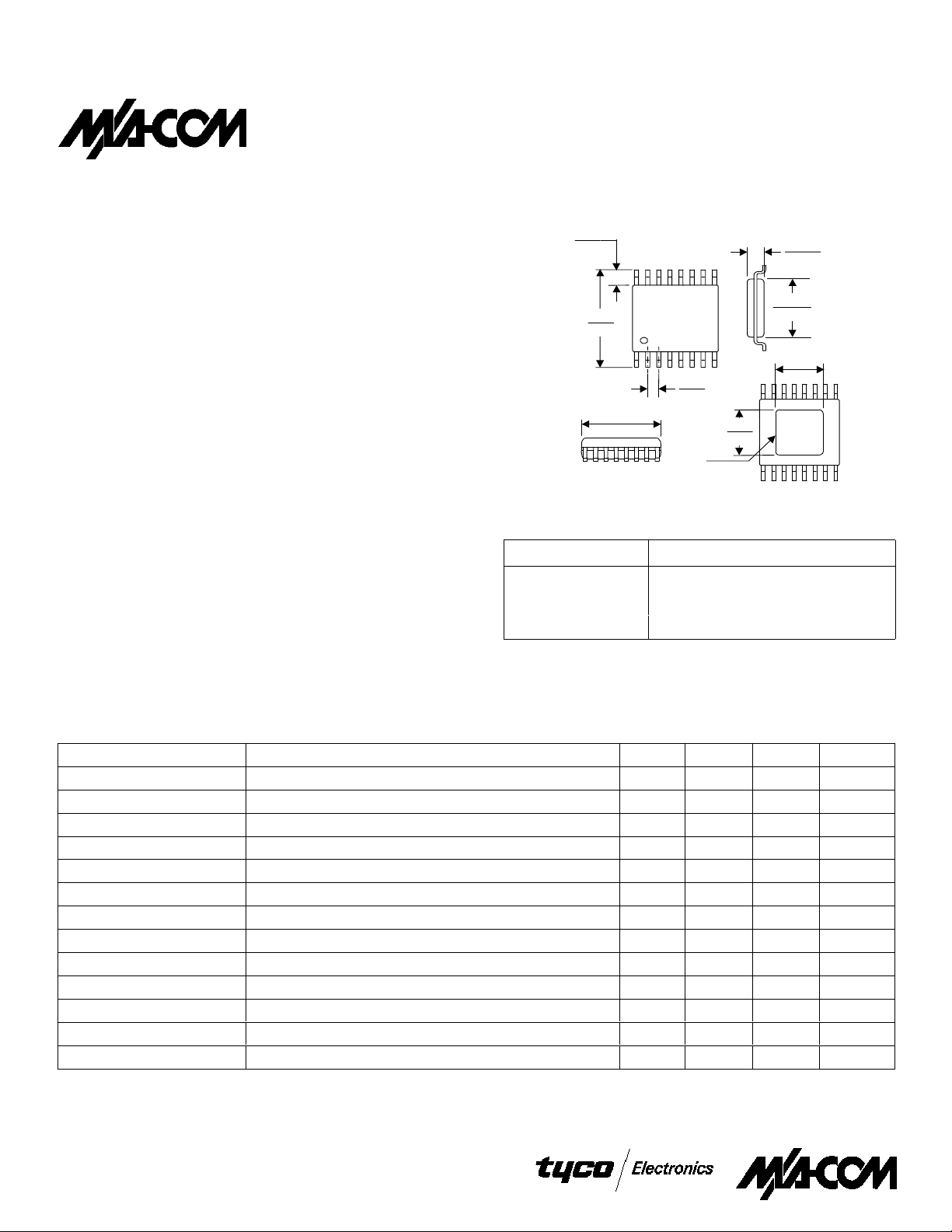
.118
3,0
1
.041/.031
1,05/,80
.177/.169
4,5/4,3
.118
3,0
TSSOP-16 Plastic Package
(.039)
Pin 16
.252
6,4
Pin 1
.201/.193
5,1/4,9
1. Dimensions are: in / mm
.0256
0,65
Exposed
Pad
Ordering Information
Part Number Package
MD59-0021TR Forward Tape and Reel
MD59-0021RTR Reverse Tape and Reel
MD59-0021SMB Sample Board
1. If specific reel size is required, consult factory for part number
assignment.
1
1
Electrical Specifications TA = 25°C, VDD = 3.0V, RF = 1.9 GHz, LO = 1.69 GHz
Parameter Test Conditions Units Min. Typ. Max.
Low Noise Amplifier
Gain Frequency = 1.9 GHz dB 14
Noise Figure dB 1.8
VSWR In/Out 2:1
Input IP
3
I
DD
Complete DownConverter
Conversion Gain dB 22.5 25.4
Noise Figure RF = 1.9 GHz dB 2.7
Input IP
3
LO-to-RF Isolation dB 50
LO-to-IF Isolation dB 24
I
DD
1. Complete downconverter measurements taken with 3 dB pad between LNA output and RFA input.
Specifications subject to change without notice.
North America: Tel. (800) 366-2266, Fax (800) 618-8883
Asia/Pacif ic: Tel.+81-44-844-8296, Fax +81-44-844-8298
Europe: Tel. +44 (1344) 869 595, Fax+44 (1344) 300 020
Visit www.macom.com for additional data sheets and product information.
dBm +6
mA 13
1
LO = 1.69 GHz, LO Level = -10 dBm dBm -12
IF = 210 MHz mA 32
V 2.0

PCS CDMA LNA / Downconverter , 1.8—2.0 GHz
MD59-0021
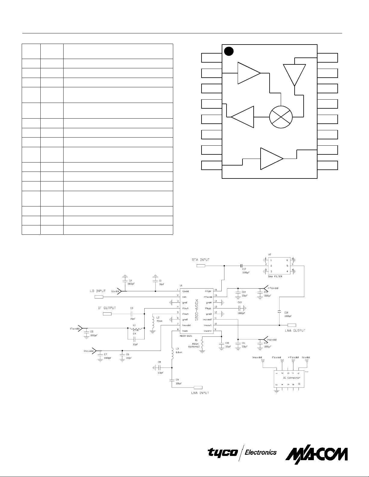
Pin Configuration
PIN No. PIN Description
1 LO V
2 LO In Local Oscillator Input (-10 to -7 dBm) (DC blocked)
3 GND DC and RF ground
4 IF Out IF Output and Downconverter - must be externally
5 IF Match Matching between I FA and Mixer - requires an inductor
6 GND DC and RF ground
7 LNA VDD1 LNA Stage 1 supply voltage. RF bypassing required.
8 LNA In RF Input to LNA. External matching required.
9 LNA SRC Source of LNA output stage FET. RF bypassing
10 LNA Out
11 LNA VDD2 LNA Stage 2 supply voltage. RF bypassing required.
12 GND DC and RF gr ound.
13 IF BYP IF Bypass of Mixer. Required DC block and RF/IF
14 GND DC and RF ground
15 RFA V
16 RFA In
LO Amplifier Supply Voltage. RF bypassing required.
DD
matched to input impedance of IF Filter.
to ground.
required. Off-chip resistor may be used to increase IP
50Ω==Output of LNA. (DC Blocked)
ground.
RFA supply voltage. RF bypassing required.
DD
50Ω==Input of RFA. (DC blocking required)
Block Diagrams
LO V
DD
LO IN
GND
IF OUT
IF MATCH
GND
1
LNA V
DD
.
3
LNA IN
RFA IN
RFA V
GND
IF BYP
GND
LNA V
DD
LNA OUT
LNA SRC 1
DD
2
Sample Board Schematic
1
J1
1. Saw filter characteristics to be determined by customer, depending on band of operation. Sample boards are supplied with 3 dB pi pad installed in
place of saw filter, to emulate typical worst case loss. Data supplied with sample board is measured over US PCS1900 Rx Band.
Specifications subject to change without notice.
North America: Tel. (800) 366-2266, Fax (800) 618-8883
Asia/Pacif ic: Tel.+81-44-844-8296, Fax +81-44-844-8298
Europe: Tel. +44 (1344) 869 595, Fax+44 (1344) 300 020
Visit www.macom.com for additional data sheets and product information.
V 2.0
 Loading...