

Low Cost MMIC Mixer, 800 - 1000 MHz MD54-0005
.
0
.
0
0
±
±
.
-
1
+
+
-
+
1
+
-
-
MD54-0005
Low Cost MMIC Mixer
800 - 1000 MHz
Features
•
+15 dBm Input Power @ 1 dB Compression
•
High Isolation, 35 dB LO to RF
•
+3 to +8 dBm LO Drive Le ve l
•
DC - 200 MHz 3 dB IF Bandwidth
•
Does not require DC bias
•
Ultra-Miniature SOT-25 plastic Package
Description
M/A-COM’s MD54-0005 is a passive mixer that achieves the
performance of a double balanced diode mixer in an ultraminiature SOT-25 package. The MD54-0005 is ideally suited
for use where high level RF signals and very wide dynamic
range are required. Typical applications include frequency
up/down conversion, modulation, and demodulation in receivers
and transmitters for basestation and portable systems.
The MD54-0005 employs GaAs FETs as mixing elements to
achieve a very wide dynamic range in a low cost plastic package. The mixer operates with LO drive levels of +3 d Bm to +8
dBm. The LO port may be externally tuned for operation in
various frequency bands.
M/A-COM's GaAs IC is fabricated using a mature 0.5 micron
gate length GaAs MESFET process. The process features full
passivation for increased performance and reliability.
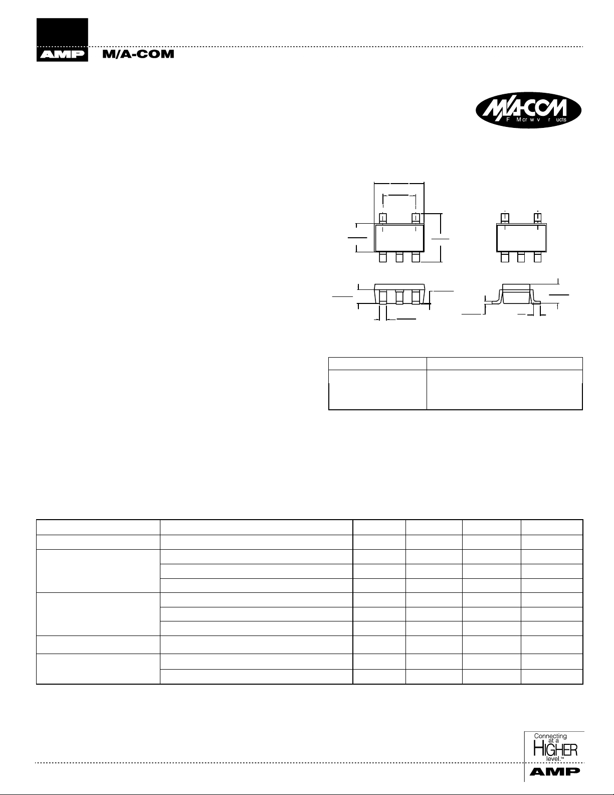
SOT-25 Plastic Package
.114±.008
0.2
2.9
.075±.008
0.20
1.90
.008
063
.031
0.80
.60
+.004
- .007
+0.10
- 0.1 8
004
0.20
0.10
.016
.40
+.004
- .002
+0.10
- 0.0 5
.110±.008
2.80± 0.20
002± .002
.05±0.05
.006
.15
.004
- .00 2
+0.10
- 0.0 5
008 MIN
0.20 MIN
.043
.10
Ordering Information
Part Number Package
MD54-0005 SOT-363 Plastic Package
MD54-0005TR Forward Tape and Reel
MD54-0005SMB Designer’s Kit
1. If specific reel size is required, consult factory for part number
assignment.
1
+.008
.004
0.20
0.10
Electrical Specifications: RF=900 MHz (-10dBm), LO=840 MHz (+5dBm), IF=60 MHz, TA = 25°C
Parameter Test Conditions Units Min. Typ. Max.
Conversion Loss dB 8.0 9.0
Isolation LO to RF dB 25 35
LO to IF dB 25
RF to IF dB 20
VSWR RF Port 2.0:1
LO Port
IF Port 2.0:1
Input 1 dB Compression RF Frequency = 900 MHz, LO = +5 dBm dBm 15
Two-Tone IM Ratio
2
Two Tones at -10 dBm each dBc 55
Tone spacing = 100 kHz, IF = 60 MHz
1. With external LO Port matching. See functional diagram on Page 2.
2. IMR vs. RF Drive can be calculated by the formula: IMR = 40-1.5* P
M/A-COM Division of AMP Incorporated 3 North America: Tel. (800) 366-2266, Fax (800) 618-8883 3 Asia/Pacific: Tel.+81 44 844 8296, Fax +81 44 844 8298
3
Europe: Tel. +44 (1344) 869 595, Fax+44 (1344) 300 020
www.macom.com
AMP and Connecting at a Higher Level are trademarks.
Specifications subject to change without notice.
1
IN
2.0:1
V2.00
Low Cost MMIC Mixer, 800 - 1000 MHz MD54-0005
1
Parameter Absolute Maximum
RF Input Power
Low Drive Power
Storage Temperature
Operating Temperature
1. Exceeding any one or combination of these limits may cause
permanent damage.
2. Ambient Temperature (T
2
2
+27 dBm
+27 dBm
-65°C to +150°C
-40°C to +85°C
) = +25°C.
A
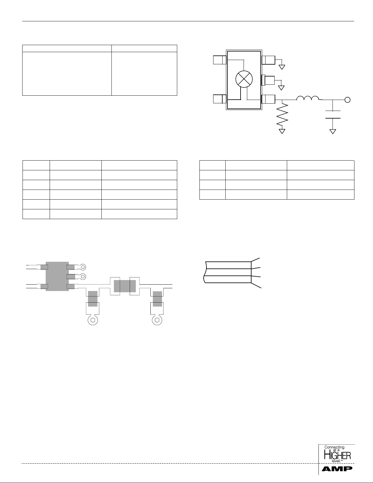
PIN Configuration
PIN No. Function Description
1 RF Port RF Input
2 IF Port IF Output
3 LO Port Lo Input
4 GND Ground
5 GND Ground
Functional Block DiagramAbsolute Maximum Ratings
RF
1
IF
23
R1
External Circuitry Parts List
Part LO = 840 MHz LO = 900 MHz
R1 820 Ohms 820 Ohms
L1 22 nH 18 nH
C1 3.3 pF 4 pF
1. All off-chip components are low-cost surface mount components
obtainable from multiple sources. (.060 in x .030 in or x .050 in)
GND
5
GND
4
L1
C1
1
LO
Recommended PCB Configuration
Layout View
L1
R1
C1
Cross Section View
RF Traces + Components
RF Ground
DC Routing
Customer Defined
The PCB dielectric between RF traces and RF ground layers
should be chosen to reduce RF discontinuities between 50
lines and package pins. M/A-COM recommends an FR-4 dielectric thickness of 0.008”(0.2 mm) yielding a 50 Ω line width of
0.015”(0.38 mm). The recommended metalization thickness is
1 oz. copper.
Ω
M/A-COM Division of AMP Incorporated 3 North America: Tel. (800) 366-2266, Fax (800) 618-8883 3 Asia/Pacific: Tel.+81 44 844 8296, Fax +81 44 844 8298
3
Europe: Tel. +44 (1344) 869 595, Fax+44 (1344) 300 020
www.macom.com
AMP and Connecting at a Higher Level are trademarks.
Specifications subject to change without notice.
V2.00

Low Cost MMIC Mixer, 800 - 1000 MHz MD54-0005
Typical Performance Curves
1, 2
Conversion Loss vs. Frequency VSWR vs. Frequency
11
10.5
10
9.5
9
8.5
8
7.5
CONVERSION LOSS (dB)
7
800 850 900 950 1000
RF FREQUE NCY (MHz)
Two-Tone IMR vs. Frequency
70
65
60
55
50
45
40
35
TWO-TONE IMR (dBc)
30
800 850 900 950 1000
RF FREQUENCY (M Hz)
RF = -10 dBm each tone
5
4.5
4
3.5
3
2.5
VSWR
2
1.5
1
0.5
0
800 850 900 950 1000
LO
RF
RF FREQUENCY (MHz)
Isolation vs. Frequency
50
45
40
35
30
25
20
15
ISOLATION (dB)
10
5
0
800 850 900 950 1000
RF to IF
LO to RF
LO to IF
RF FREQUENCY (MHz)
1. Test Conditions for Down Converter Application: RF=900 MHz (-10 dBm), IF=60 MHz, LO=840 MHz (+5 dBm), LO Port match shown on Page 2.
2. Test Conditions for Up Converter Application: LO=840 MHz (+5 dBm), IF=60 MHz (-10 dBm), RF=900 MHz, LO Port match shown on Page 2.
Spurious Table (dBc)
(n) 4x 23.0 36.5 53.8 63.8 68.6
H
a
r
m
o
n
i
c
10.6 39.9 56.1 58.3 58.8
3x 34.1 21.6 53.9 53.4 67.3
21.3 21.8 57.6 59.3 57.2
2x 17.7 44.0 51.6 65.2 66.2
6.6 44.8 55.5 58.4 56.3
1x 14.3 0 57.0 63.7 67.0
4.0 0 57.6 56.3 56.9
0x X 13.9 50.2 59.1 67.2
X 13.4 53.1 56.5 57.1
of
0x 1x 2x 3x 4x
LO Harmonic of RF (m)
The spurious table shows the spurious signals resulting from the
mixing of the RF and LO input signals assuming down conversion. Mixing products are indicated relative to the IF. The lower
frequency mixing term is shown for two different RF input
levels. The upper number is for an RF input power of 0 dBm;
the lower number is for an RF level of -10 dBm.
|nF
|nF
RF -mFLO
RF - mFLO
|, (RF =0 dBm)
|, (RF = -10 dBm)
RF Frequency = 900 MHz
LO Frequency = 840 MHz
M/A-COM Division of AMP Incorporated 3 North America: Tel. (800) 366-2266, Fax (800) 618-8883 3 Asia/Pacific: Tel.+81 44 844 8296, Fax +81 44 844 8298
3
Europe: Tel. +44 (1344) 869 595, Fax+44 (1344) 300 020
www.macom.com
AMP and Connecting at a Higher Level are trademarks.
Specifications subject to change without notice.
V2.00

Low Cost MMIC Mixer, 800 - 1000 MHz MD54-0005
S
A
L
R
Designer’s Kit MD54-005SMB
The MD54-0005SMB Designer's Kit allows for immediate evaluation of M/A-COM's MD54-0005. The evaluation board consists of an MD54-0005, recommended external surface mount
circuitry, and RF connectors, all mounted to a multi-layer FR-4
PCB. Other items included in the Designer's Kit are a floppy
disk (with typical performance data and a DXF file of the
recommended PCB layout) and any additional Application
Notes. The MD54-0005SMB evaluation PCB and block diagram are illustrated below with all functional ports labeled.
Evaluation PCB & RF Connector Losses
Port Reference Approximate RF Loss
RF Port 0.10 dB @ 900 MHz
LO Port 0.10 dB @ 900 MHz
IF Port 0.05 dB @ 60 MHz
Mixer PCB
F
IF
O
OT MIX ER
V1004 6
V2.00
M/A-COM Division of AMP Incorporated 3 North America: Tel. (800) 366-2266, Fax (800) 618-8883 3 Asia/Pacific: Tel.+81 44 844 8296, Fax +81 44 844 8298
3
Europe: Tel. +44 (1344) 869 595, Fax+44 (1344) 300 020
www.macom.com
AMP and Connecting at a Higher Level are trademarks.
Specifications subject to change without notice.
 Loading...