M A COM MASW6020G Datasheet

GaAs SPST Switch
DC-6 GHz MASW6020G
Features
• Low Insertion Loss,0.6 dB Typical @ 1 GHz
• Fast Switching Speed,10 ns Typical
• Ultra Low DC Power Consumption
• Integral Static Protection
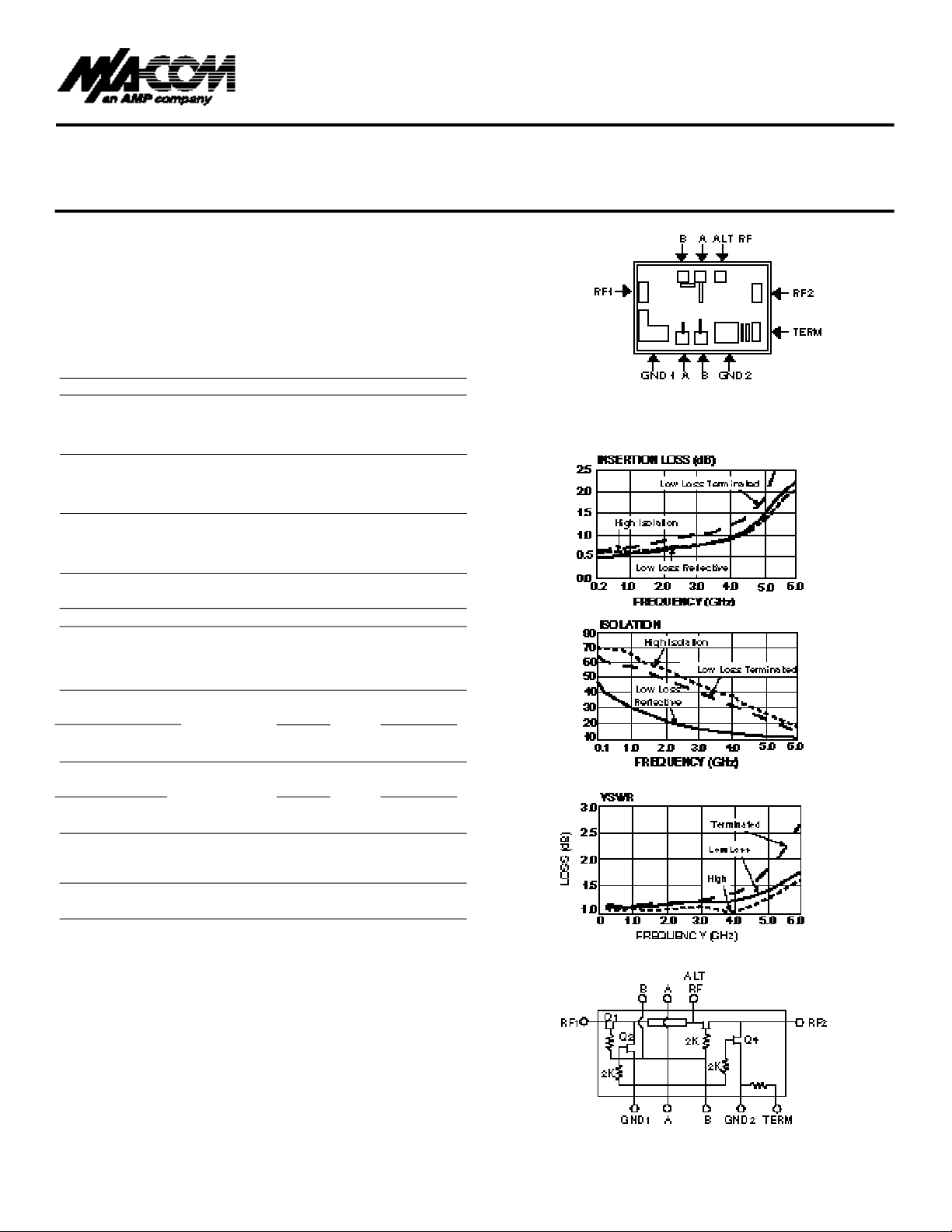
Guaranteed Specifications** @25°C***
Frequency Range DC - 6000 MHz
Insertion Loss (L) Low Loss Low Loss Matched (H) High Isolation
DC-1.0 GHz 0.8 dB 1.0 dB 0.9 dB
DC-2.0 GHz 0.9 dB 1.1 dB 1.0 dB
DC-6.0 GHz 2.5 dB 2.7 dB 2.5 dB
Isolation (L) Low Loss Low Loss Matched (H) High Isolation
DC-1.0 GHz 30 dB 63 dB 64 dB
DC-2.0 GHz 22 dB 46 dB 52 dB
DC-6.0 GHz 11 dB 14 dB 19 dB
VSWR (L) Low Loss Low Loss Matched (H) High Isolation
DC-1.0 GHz 1.1:1 1.1:1 1.1:1
DC-2.0 GHz 1.3:1 1.2:1 1.1:1
DC-6.0 GHz 2.0:1 2.7:1 2.0:1
Operating Characteristics
Impedance 50 Ω Nominal
Switching Characteristics
Trise, Tfall (10%/90% or 90%/10% RF) 10 ns Typ
Ton, Toff (50% CTL to 90%/10% RF) 10 ns Typ
Transients (In-Band) 10 mV Typ
Input Power for 1 dB Compression
Control Voltages (VDC) 0/-5 0/-8
Above 500 MHz +27 dBm +33 dBm Typ
100 MHz +21 dBm +26 dBm Typ
Intermodulation Intercept Point (for two-tone input power up to +5 dBm)
Intercept Points IP2 IP3
Above 500 MHz +68 dBm +46 dBm Typ
100 MHz +62 dBm +40 dBm Typ
Control Voltages (Complementary Logic)
Vin Low 0 to -0.2V @ 20 µA Max
Vin Hi -5V @ 50 µA Typ to -8V @ 300 µA Max
Die Size 0.031" x 0.051" x 0.010"
(0.80 mm x 01.30 mm x 0.25 mm)
* Equivalent to Microelectronics Division (ANZAC) SW210H
** All specifications apply with 50 Ω impedance connected to all RF
ports, 0 and -8 VDC control voltages.
*** Loss change 0.0025 dB/°C. (From -55°C to +85°C)
V 2.00
Typical Performance
Schematic

Handling, Mounting, and Bonding Procedure MASW6020G
Truth Table
Maximum Ratings
Control Voltage (A/B): -8.5 VDC
Max Input RF Power: +34 dBm
(500 MHz - 4 GHz)
Storage Temperature: -65°C to +175°C
Maximum Operating Temperature: +175°C
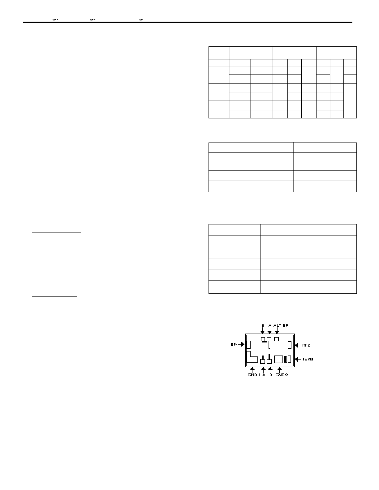
RF1, RF2: 0.004 x 0.006 (0.100 x 0.150)
Alt RF: 0.004 x 0.005 (0.100 x 0.125)
A,B: 0.004 x 0.004 (0.100 x 0.100)
GND1: 0.012 x 0.007 (0.300 x 0.175)
GND2 : 0.009 x 0.008 (0.225 x 0.200)
Term: 0.004 x 0.008 (0.100 x 0.200)
Switch Condition
Option Control Voltage & Bonding Ground Bonds
A B RF1 RF2 ALT GND1 GND2 Term
V Hi V Low on on G G
V Low V Hi off off G G
V Hi V Low on on G G
V Low V Hi off off G G
V Hi V Low on on G G
V Low V Hi off off G G
Handling Precautions
Permanent damage to the MASW6020G may occur if the following
precautions are not adhered to:
A. Cleanliness – The MASW6020G should be handled in a clean
e nv i r o n m e n t . DO NOT attempt to clean unit after the
MASW6020G is installed.
B. Static Sensitivity – All chip handling equipment and personnel
should be DC grounded.
C. Transient – Avoid instrument and power supply transients while
bias is applied to the MASW6020G. Use shielded signal and
bias cables to minimize inductive pick-up.
D. Bias – Apply voltage to either control port A/B or only when the
other is grounded. Neither port should be allowed to “float.”
T
L
H
V 2.00
E. General Handling – It is recommended that the MASW6020G
chip be handled along the long side of the die with a sharp pair
of bent tweezers. DO NOT touch the surface of the chip with
fingers or tweezers.
Mounting
The MASW6020G is back - m e t a l l i zed with Pd/Ni/Au (100/1,000/
30,000Å) metallization. It can be die-mounted with AuSn eutectic
preforms or with thermally conductive epoxy. The package surface
should be clean and flat before attachment.
Eutectic Die Attach:
A. A 80/20 gold/tin preform is recommended with a work surface
temperature of approximately 255°C and a tool temperature of
265°C. When hot 90/10 nitrogen/hydrogen gas is applied, tool
tip temperature should be approximately 290°C.
B. DO NOT expose the MASW6020G to a temperature greater
than 320°C for more than 20 seconds.No more than 3 seconds
of scrubbing should be required for attachment.
Epoxy Die Attach:
A. Electrically conductive epoxy must be used.
B. Apply a minimum amount of epoxy and place the MASW6020G
into position. A thin epoxy fillet should be visible around the
perimeter of the chip.
Bond Pad Dimensions – Inches (mm)
Bond Pad Layout
C. Cure epoxy per manufacturer's recommended schedule.
Wire Bonding
A. Ball or wedge bond with 1.0 mil diameter pure gold wire.T h e rm o -
sonic wirebonding with a nominal stage temperature of 150°C
and a ball bonding force of 40 to 50 grams or wedge bonding
force of 18 to 22 grams is recommended.U l t rasonic energy and
time should be adjusted to the minimum levels to achieve reliabl e
w i r e b o n d s.
B. Wirebonds should be started on the chip and terminated on the
p a ck a g e.
 Loading...