M A COM MASW2040 Datasheet

GaAs DPDT Switch
DC - 2 GHz M A S W 2 0 4 0
V 2.00
●
C a s c a d a b l e
●
Low Insertion Loss
●
Low DC Power Consumption
●
Low Distortion Operation (Quiet Mode)
Useful as a Building Block for
●
– Digital Attenuators
– Digital Delay Lines
– Digital Phase Shifters
– Digital Switched Filter Elements
Guaranteed Specifications** -55°C to +85°C
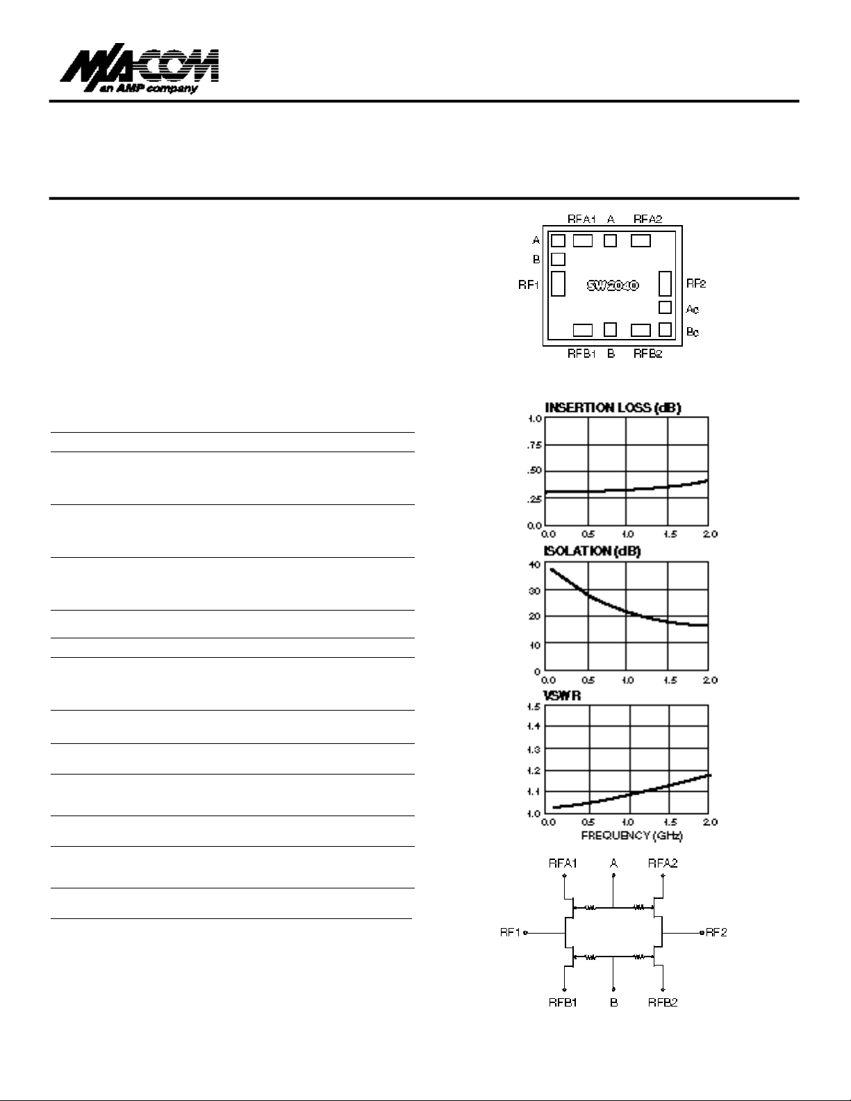
Frequency Range DC – 2.0 GHz
Insertion Loss
DC – 0.5 GHz 0.4 dB Max
DC – 1.0 GHz 0.4 dB Max
DC – 2.0 GHz 0.6 dB Max
VSWR
DC – 0.5 GHz 1.1:1 Max
DC – 1.0 GHz 1.2:1 Max
DC – 2.0 GHz 1.2:1 Max
Isolation
DC – 0.5 GHz 25 dB Min
DC – 1.0 GHz 20 dB Min
DC – 2.0 GHz 15 dB Min
Typical Pe r formance @ +25°C
Operating Characteristics
Impedance 50 Ω Nominal
Switching Characteristics
tRISE, tFALL (10/90% or 90/10% RF) 3 ns Typ
tON, tOFF (50% CTL to 90/10% RF) 6 ns Typ
Transients (In-Band) 20 mV Typ
Input Power for 1dB Compression
Control Voltages (Vdc) 0/–5 0/–8
0.05 GHz +24 dBm +25 dBm Typ
0.5 - 2 GHz +30 dBm +33 dBm Typ
Intermodulation Intercept Point
(for two-tone input power up to +5 dBm)
Intercept Points IP2 IP3
0.05 GHz +62 +39 dBm Typ
0.5 - 2 GHz +68 dBm +46 dBm Typ
Control Voltages (Complementary Logic)
VINLow 0 to –0.2V @ 9 µA Max
VINHi –5V @ 25 µA Typ to –8V @ 75 µA Max
Die Size 0.045" x 0.038" x 0.010"
(1.13mm x 0.97mm x 0.25mm)
**All specifications apply with 50 Ω impedance connected to all RF
ports, 0 and –5 Vdc control voltages.
*** Loss change 0.0025dB/°C (-55°C to +85°C)
S ch e m a t i c

H a n d l i n g ,M o u n t i n g , Bonding Pro c e d u r e M A S W 2 0 4 0
Maximum Ratings
A. Control Value (A or B): –8.5 Vdc
B. Max Input RF Power: +34 dBm
(500 MHz–4 GHz)
C. Storage Temperature: –65°C to +175°C
D. Max Operating Temperature: +175°C
BondPad Dimensions — Inches (mm)
RF1, RF2 0.004 x 0.008 (0.100 x 0.200)
RFA1, RFB1 0.004 x 0.005 (0.100 x 0.125)
RFA2, RFB2 0.004 x 0.005 (0.100 x 0.125)
A, B, Ac, Bc 0.004 x 0.004 (0.100 x 0.100)
Truth Ta bl e
VINLOW= 0.0 TO -0.2V
VINH
I = -0.5V
Die Size — Inches (mm)
0.045 x 0.038 x 0.010 (1.13 x 0.97 x 0.25)
V 2.00
Handling Precautions
Permanent damage to the MASW2040 may occur if the following
precautions are not adhered to:
A. Cleanliness — The MASW2040 should be handled in a clean
environment. DO NOT attempt to clean unit after the
MASW2040 is installed.
B. Static Sensitivity — All chip handling equipment and personnel
should be DC grounded.
C.Transient — Avoid instrument and power supply transients
while bias is applied to the MASW2040.Use shielded signal
and bias cables to minimize inductive pick-up.
D. Bias — Apply voltage to either control port A or B only when
the other is grounded. Neither port should be allowed to
“float”.
E. General Handling — It is recommended that the MASW2040
chip be handled along the long side of the die with a sharp
pair of bent tweezers. DO NOT touch the surface of the chip
with fingers or tweezers.
Mounting
The MASW2040 is back-metallized with Pd/Ni/Au(100/1,000/
10,000Å) metallization. It can be die-mounted with AuSn eutectic
preforms or with thermally conductive epoxy. The package surface should be clean and flat before attachment.
Control Inputs Condition of Switch
A B RF1 - RFA1 RF1 - RFB1 RF2 - RFA2 RF2 - RFB2
VINHIVINL
VINL
OW
OW
VINH
OFF ON OFF ON
I ON OFF ON OFF
Eutectic Die Attach:
A. A 80/20 gold/tin preform is recommended with a work surface
temperature of approximately 255°C and a tool temperature of
265°C.When hot 90/10 nitrogen/hydrogen gas is applied, tool
tip temperature should be approximately 290°C.
B. DO NOT expose the MASW2040 to a temperature greater
than 320°C for more than 20 seconds. No more than 3
seconds of scrubbing should be required for attachment.
Epoxy Die Attach:
A. Apply a minimum amount of epoxy and place the MASW2040
into position. A thin epoxy fillet should be visible around the
perimeter of the chip.
B. Cure epoxy per manufacturer’s recommended schedule.
C. Electrically conductive epoxy may be used but is not required.
Wire Bonding
A. Ball or wedge with 1.0 mil diameter pure gold wire.
Thermosonic wirebonding with a nominal stage temperature
of 150°C and a ball bonding force of 40 to 50 grams or wedge
bonding force of 18 to 22 grams is recommended. Ultrasonic
energy and time should be adjusted to the minimum levels
achieve reliable wirebonds.
B. Wirebonds should be started on the chip and terminated on
the package. GND bonds should be as short as possible; at
least three and no more than four bond wires from ground
 Loading...