M A COM MA4SPS302 Datasheet

MA4SPS302 SurMount Series
Surface Mount Monolithic
PIN Diode Chip
Features
• Surface Mount Diode
• No Wirebonds Required
• Rugged Silicon-Glass Construction
• Silicon Nitride Passivation
• Polymer Scratch Protection
• Low Parasitic Capacitance and Inductance
• High Power Handling (Efficient Heatsinking)
Description
M/A-COM’s MA4SPS302 is a silicon-glass PIN diode
fabricated with M/A-COM’s patented HMIC™ process. This
device features two silicon pedestals embedded in a low loss
glass. The diode is formed on the top of one pedestal and
connections to the backside of the device are facilitated by
making the pedestal side walls conductive. Selective backside
metalization is applied producing a surface mount device. The
topside is fully encapsulated with silicon nitride and has an
additional polymer layer for scratch protection. These
protective coatings prevent damage to the junction and the
anode air-bridge during handling and assembly.
Applications
These devices can be used in series and shunt switches for
wireless circuits where smaller area and profile are required.
Low parasitic values of L and C make additional circuit tuning
unnecessary. 2 RS value @ 1 mA makes the devices suitable
for smaller current consumption applications.
Ω
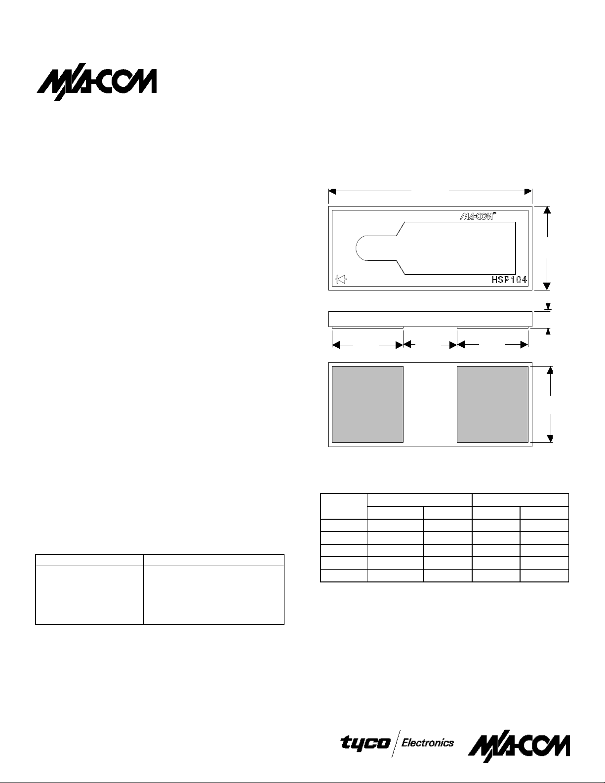
Case Style
ODS-1247
1. Backside metal: 0.1 micron thk. gold.
2. Hatched areas indicate bond pads.
1, 2
A
D E
B
C
D
D
Absolute Maximum Ratings1
@ TA = +25°C (unless otherwise specified)
Parameter Absolute Maximum
Reverse Voltage -70 V
Forward Current 100 mA
Operating Temperature -65°C to +150°C
Storage Temperature -65°C to +150°C
Mounting Temperature +235°C for 10 seconds
1. Exceeding these limits may cause permanent damage.
Specifications subject to change without notice.
n North America: Tel. (800) 366-2266, Fax (800) 618-8883
n Asia/Pacific: Tel.+81-44-844-8296, Fax +81-44-844-8298
n Europe: Tel. +44 (1344) 869 595, Fax+44 (1344) 300 020
Visit www.macom.com for additional data sheets and product information.
INCHES
DIM.
A 0.0520 0.0583 1.320 1.480
B 0.0201 0.0264 0.510 0.670
C 0.0040 0.0080 0.102 0.203
D 0.0180 0.0200 0.457 0.508
E 0.0140 0.0160 0.355 0.406
MIN. MAX. MIN. MAX.
MILLIMETERS
V 2.0
1

Surface Mount Monolithic PIN Diode Chip
MA4SPS302 SurMount Series
Electrical Specifications @ +25°C
Symbol Test Conditions Units Min. Typ. Max.
CT -40 Volts, 1 MHz 1 pF 0.400 0.450
CT -40 Volts, 1 GHz
RS 10 mA, 100 MHz
RS 10 mA, 1 GHz
VF 10 mA V 0.84 1.00
VR
10 µA
IR -70V
TL 10 mA / 6 mA ns 460
1. Total capacitance is equivalent to the sum of junction capacitance Cj and parasitic capacitance.
2. Series resistance R
3. R
and CP is measured on an HP4291A with die mounted in an ODS-186 package with conductive silver epoxy.
S
is equivalent to the total diode series resistance including the junction resistance Rj.
S
1, 3
pF 0.300
2,
2, 3
Ω
Ω
1.0
1.3
V -70 -120
µA
10
Handling Procedures
All semiconductor chips should be handled with care to avoid
damage or contamination from perspiration and skin oils. The
use of plastic tipped tweezers or vacuum pickups is strongly
recommended for individual components. Bulk handling should
insure that abrasion and mechanical shock are minimized.
ESD
These devices very susceptible to ESD and are rated Class 0
(0-199V) per HBM MIL-STD-883, method 3015.7 [C = 100pF
±10%, R = 1.5kΩ ±1%]. Even though tested die pass 100V
ESD, they must be handled in a static-free environment.
Bonding Techniques
Attachment to a circuit board is made simple through the use of
surface mount technology. Mounting pads are conveniently
located on the bottom surface of these diodes and are removed
from the active junction locations. These diodes are well suited
for solder attachment onto hard and soft substrates. The use of
80/20 Au/Sn and 60/40 Sn/Pb solder is recommended.
Conductive epoxy paste for attachment may also be used, this
can be silk-screened, or used with a conductive sheet apoxy.
When soldering these diodes to a hard substrate, hot gas die
bonding is preferred. We recommend utilizing a vacuum tip and
a force of 60 to 100 grams applied normal to the top surface of
the part. When soldering to soft substrates, it is recommended
to use a lead-tin interface at the circuit board mounting pads.
Position the die so that its mounting pads are aligned with the
circuit board’s mounting pads Reflow the solder by heating the
circuit trace near the mounting pad while applying 60 to 100
grams of force perpendicular to the top surface of the die.
Since the HMIC™ glass is transparent, the edges of the
mounting pads closest to each other can be visually inspected
through the die after attach is completed.
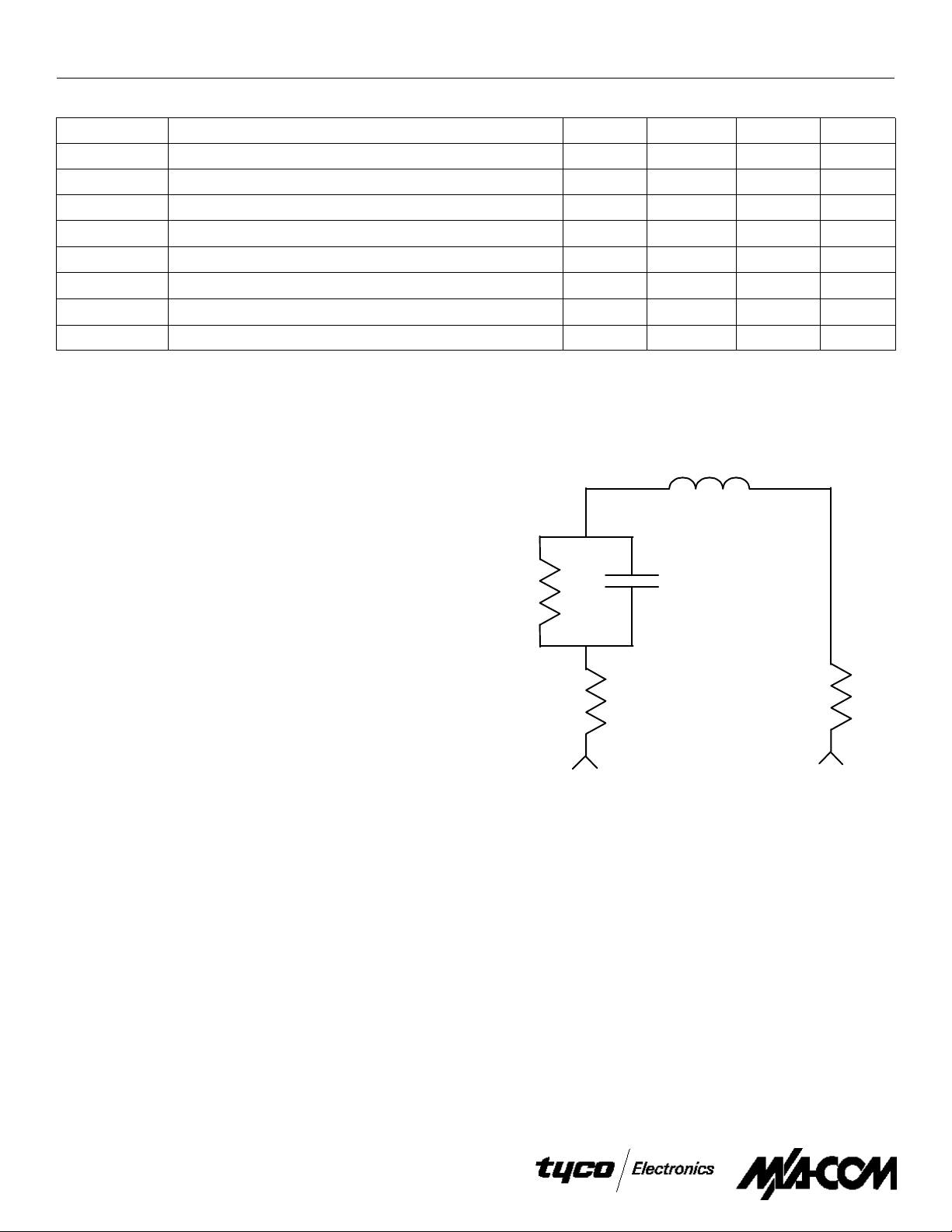
Functional Schematic1
Cp
Rp
Rvia
-
1. Rs = 2 * Rvia + Rp
Ls
Rvia
+
Specifications subject to change without notice.
n North America: Tel. (800) 366-2266, Fax (800) 618-8883
n Asia/Pacific: Tel.+81-44-844-8296, Fax +81-44-844-8298
n Europe: Tel. +44 (1344) 869 595, Fax+44 (1344) 300 020
Visit www.macom.com for additional data sheets and product information.
V 2.0
2
 Loading...