M A COM MA4BPS201, MA4BPS101, MA4BPS301 Datasheet

PIN Diode Chips With Offset Bond Pads MA4BPS101, MA4BPS201, MA4BPS301
g
MA4BPS101, MA4BPS201, MA4BPS301
PIN Diode Chips with
Offset Bond Pads
Features
•
Bond Pads Removed From Active Junction
•
Large Bond Pads Support Multiple Bond Wires
•
Rugged Silicon-Glass Construction
•
Silicon Nitride Passivation
•
Polyimide Scratch Protection
Description
These silicon - glass PIN diode chips are fabricated with
M/A-COM’s patented HMIC™ process. They contain a single
shunt silicon PIN diode embedded in a glass s ubstrate with dual
75 x 150 micron bond pads located near the chip edges. The large
pads allow use of multiple bond wires. The location of these pads
on a glass substrate results in low parasitic capacitance. The
diode junction is passivated with silicon nitride and a layer of
polyimide has been added for scratch protection during assembly.
The devices are available on industry standard tape frame for
automatic insertion and assembly in high volume applications.
Applications
These diodes are designed for use as general PIN elements in
switches and switched pad attenuators. The chips can handle up
to 10 watts of RF power, and are well suited for use in T/R
switches for subscriber phones, particularly the higher power and
higher frequency systems for satellite based systems. They are
also useful for the switching element in phased array radar applications. The larger bond pad allows for two (2) 1 mil dia contact
wires which reduces the bond wire inductance almost in half.
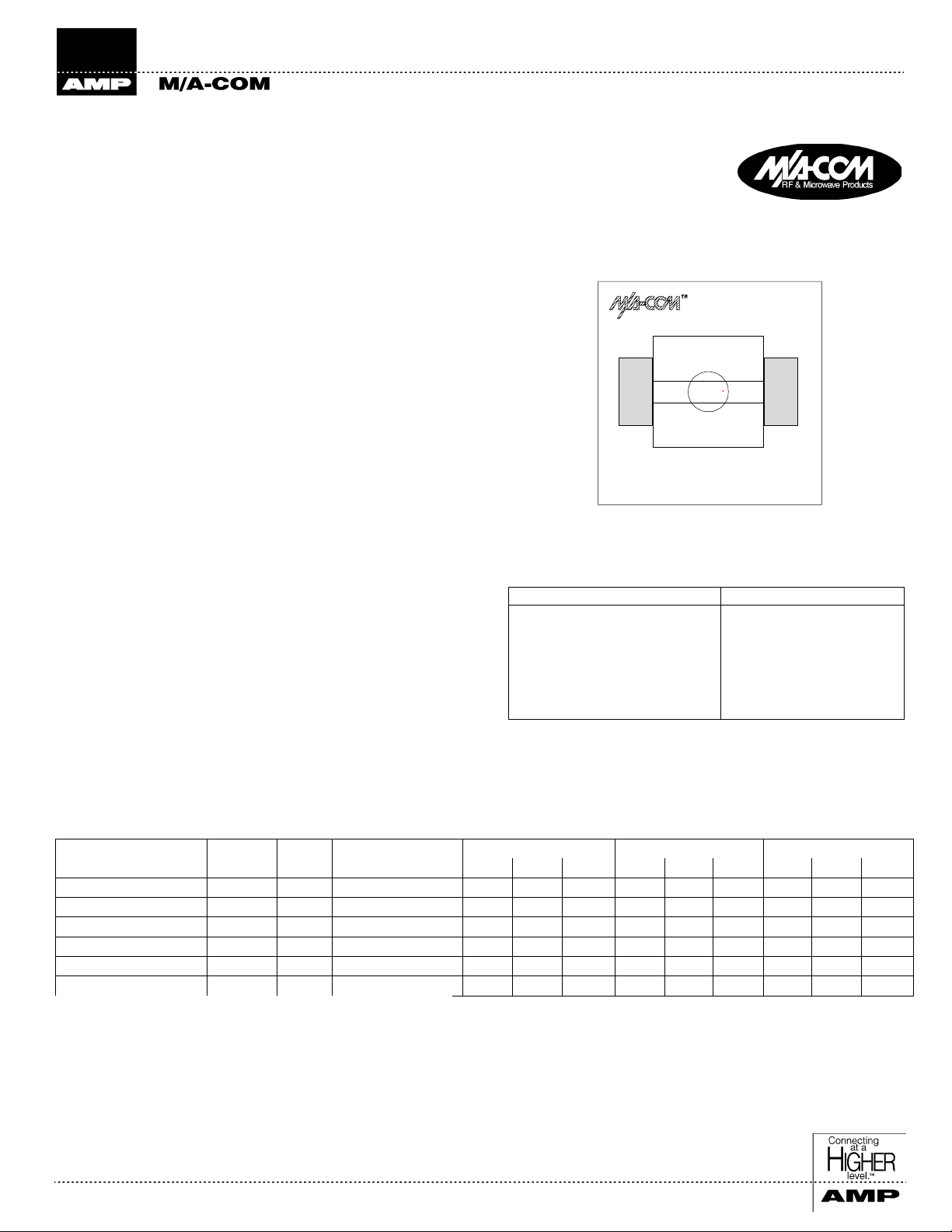
Chip Layout
Absolute Maximum Ratin
Parameter Absolute Maximum
Operating Temperature
Storage Temperature
Forward Current 100mA
Reverse Voltage 70 V
Incident RF Power +40 dBm (CW)
Mounting Temperature
1. Exceeding these limits may cause permanent damage.
1
-60°C to +150°C
-65°C to +175°C
+320°C for 10 seconds
Electrical Specifications @ +25°C
MA4BPS101 MA4BPS201 MA4BPS301
Parameters Symbol Units Test Conditions M in. Typ. Max. Min. Typ. Max. Min. Typ. Max.
Total Capacitance C
Series Resistance
Parallel Resistance
Breakdown Voltage Vb Volts -10 uA 70 110 70 110 70 110
Carrier Lifetime
Thermal Impedance
1. Guaranteed by correlation to 2 MHz on-wafer measurements.
2. Tested on a sample basis only.
M/A-COM Division of AMP Incorporated Q North America: Tel. (800) 366-2266, Fax (800) 618-8883 Q Asia/Pacific: Tel.+85 2 2111 8088, Fax +85 2 2111 8087
Q Europe: Tel. +44 (1344) 869 595, Fax+44 (1344) 300 020
www.macom.com
1
2
2
2
T
Rs
Rp
T
L
jc
θ
AMP and Connecting at a Higher Level are trademarks.
Specifications subject to change without notice.
pF -5 Volts at 1 MHz 0.13 0.17 0.20 0.25 0.30 0.35
Ω
+10 mA at 1 GHz 1.9 2.4 1.0 1.3 0.9 1.2
K
Ω
0 Volts at 1 GHz 14 6 6
nS +10mA/-6mA 300 300 300
C/W
°
1A/.01A, 10 mS 38 28 24
V2.01

PIN Diode Chips With Offset Bond Pads MA4BPS101, MA4BPS201, MA4BPS301
)
(
)
Hanlding and Mounting Information
Handling
All semiconductor dice should be handled with care to avoid
damage or contamination. For an individual die, the use of
plastic tipped tweezers or vacuum pick-up tool is recommended.
When using automatic pick and place, abrasion and mechanical
shock should be minimized.
Mounting
The dice have Ti-Pt-Au back metal, with a final gold thickness
of 0.1 micron. They can be die mounted with a gold-tin eutectic
solder preform or conductive epoxy. The mounting surface
must be clean and flat.
Eutectic Die Attachment
An 80/20 gold-tin eutectic solder preform is recommended with
a work surface temperature of 255
°
of 265
should be 290
tures greater than 320
C. When hot gas is applied, the tool tip temperature
°
C. The chip should not be exposed to tempera-
°
C for more than 20 seconds. No more
than three seconds should be required for attachment.
Epoxy Die Attachment
A minimum amount of epoxy should be used. A thin epoxy
fillet should be visible around the perimeter of the chip after
placement. Cure epoxy per manufacturer’s schedule.
Wire Bonding
The two bond pads on these die have a Ti-Pt-Au metalization
scheme, with a final gold thickness of 2.5 microns. Th e pa ds are
75 x 150 microns; up to two wires or a 100 micron wide ribbon
can be bonded to each pad. Thermosonic wedge wire bonding of
0.001” diameter gold wire is recommended with a stage temperature of 150
°
C and a force of 25 to 40 grams. Ultra sonic e n e rgy
should be adjusted to the minimum required.
°
C and a tool tip temperature
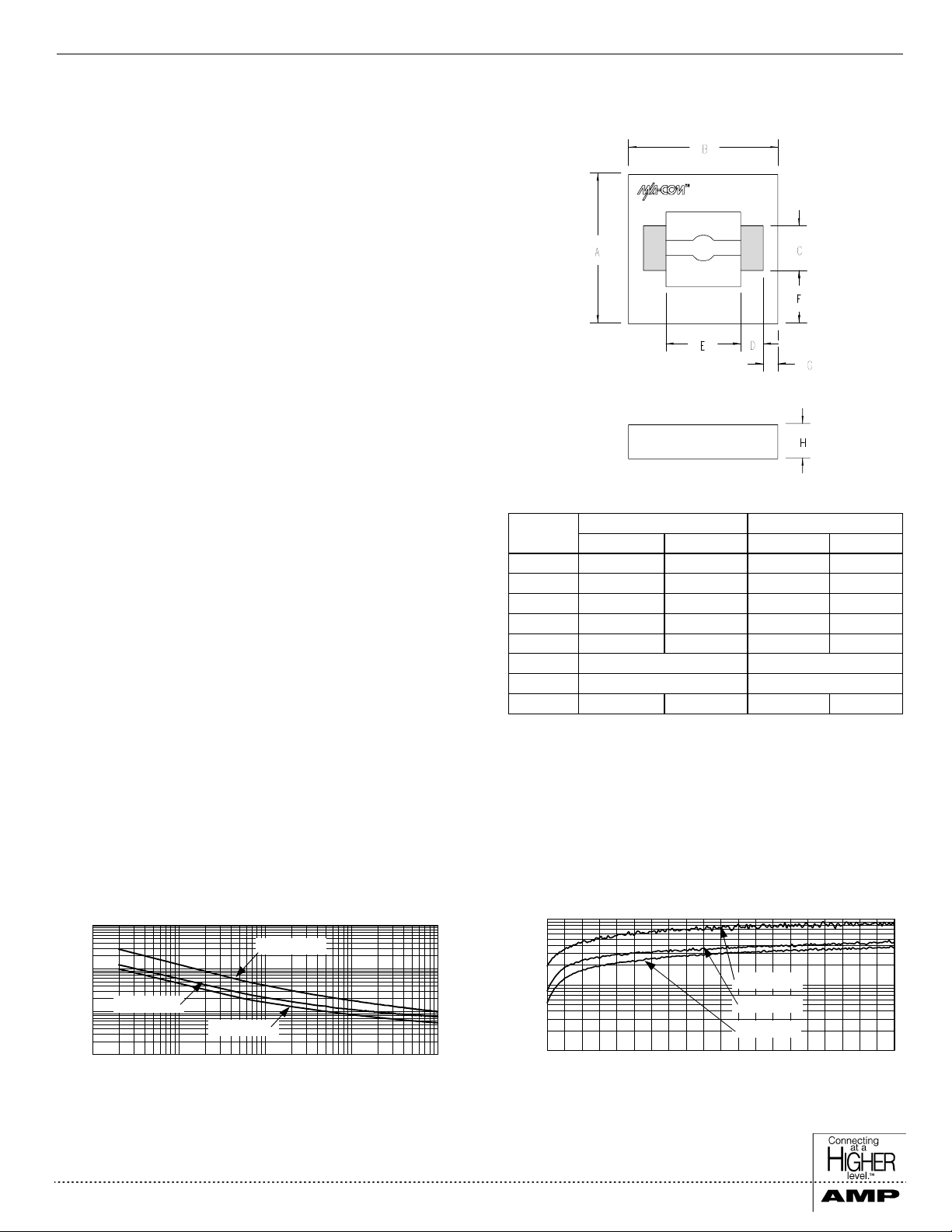
Chip Outline Drawing (ODS-1244
INCHES MILLIMETERS
DIM
A
B
C
D
E
F
G
H
Notes: 1. Bond pad material: 2.5 micron thick gold.
MIN MAX MIN MAX
0.019 0.0213 0.480 0.540
0.019 0.0213 0.480 0.540
0.0055 0.0063 0.140 0.160
0.0026 0.0033 0.065 0.085
0.0094 0.0102 0.240 0.260
0.007 Ref. 0.180 Ref.
0.002 Ref. 0.050 Ref.
0.0043 0.0055 0.110 0.140
2. Shaded areas indicate wire bonding pads
3. Backside metal: 0.1 micron thick gold.
Typical Resistance Curves
Series Resistance vs. Forward Current at 1 GHz Parallel Resistance vs. Reverse Voltage at 1 GHz
100.0
MA4BPS101
10.0
MA4BPS201
1.0
Series Resistance (Ohms)
0.1
0.0 0.1 1.0 10.0 100.0
M/A-COM Division of AMP Incorporated Q North America: Tel. (800) 366-2266, Fax (800) 618-8883 Q Asia/Pacific: Tel.+85 2 2111 8088, Fax +85 2 2111 8087
Q Europe: Tel. +44 (1344) 869 595, Fax+44 (1344) 300 020
www.macom.com
MA4BPS301
F o r w a r d C u r r e n t ( m A )
AMP and Connecting at a Higher Level are trademarks.
Specifications subject to change without notice.
100,000
Ohms
10,000
Parallel Resistance
1,000
0.0 2.0 4.0 6.0 8.0 10.0
R e v e r s e V o l t a g e ( V o l t s )
MA4BPS101
MA4BPS201
MA4BPS301
V2.01
 Loading...