M A COM MA02305AK-SMB, MA02305AK-R7 Datasheet

3.0 V 100 mW RF Power Amplifier
IC for Bluetooth
V 1.00
MA02305AK
Features
n 20 dB Gain – dramatically increases range of your low
power Bluetooth devices
n Single 3.0V positive supply – operates over a wide
range of supply voltages
n Extremely small size – 6 pin SOT plastic package -
3 mm x 1.75 mm body size
n Output power easily controllable via V
n 45% Power Added Efficiency
n 100% Duty Cycle
n 2000 to 2900 MHz Operation
n Self-Aligned MSAG
®
-Lite MESFET Process
DD1
Description
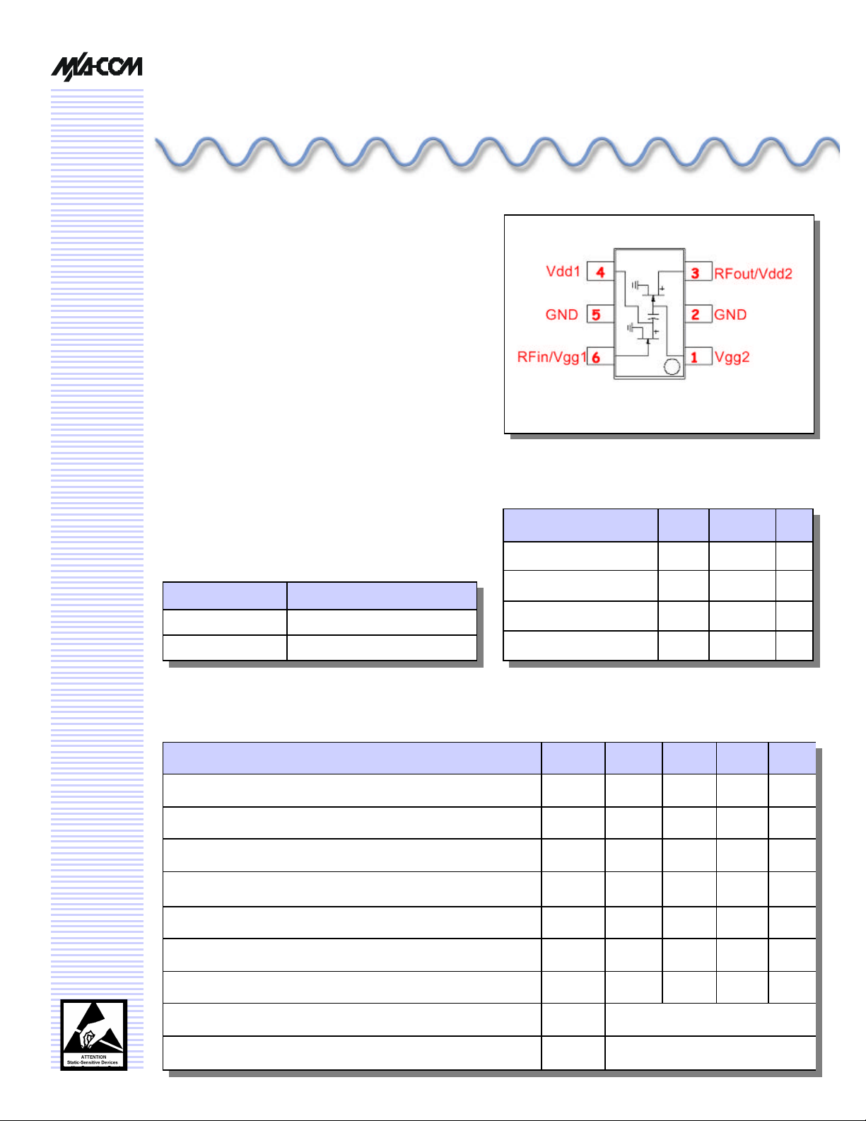
The MA02305AK is an RF power am plifier based on M/ACOM’s Self-Aligned MSAG MESFET Process. This
product is designed for use in 2.4 GHz ISM products as a
booster for high power Bluetooth devices. Output power
can be controlled to meet Bluetooth requirements via varying input power or the voltage on V
DD1
.
Ordering Information
Part Number Package
MA02305AK-R7 7 inch, 3000 Piece Reel
MA02305AK-SMB MA02305AK Test Board
MA02305AK
Maximum Ratings (T
Rating
DC Supply Voltage VDD 5.5 V
RF Input Power PIN 10 mW
Junction Temperature TJ 150 °C
Storage Temperature Range T
= 25 °C unless otherwise noted)
A
Symbol Value Unit
-40 to +150 °C
STG
Electrical Characteristics: V
Characteristic Symbol Min Typ Max Unit
Frequency Range ƒ 2400 2500 MHz
Output Power f = 2450 MHz P
Power Added Efficiency f = 2450 MHz η 40 45 %
Harmonics 2ƒ
Input VSWR - 1.5 2.0 :1
Off Isolation (VDD=0 V) S21 -25 dB
Thermal Resistance, junction to soldering point (pin 2) RTH 180 °C/W
Load Mismatch (VDD = 5.5 V, VSWR = 8:1, PIN = 0 dBm) - No Degradation in Power Output
Stability (P
= 0dBm, VDD = 0-5.5 V, Load VSWR = 5:1, fixed phases) - All non-harmonically related outputs
IN
= 2.5 V, V
DD1
= 3 V, P
DD2
= +0 dBm, Duty Cycle = 100%, T
IN
18.7 20 dBm
OUT
3ƒ
-30
-27
more than 60 dB below desired signal
A
-26
-22
= 25°C
dBc

3.0 V 100 mW RF Power Amplifier IC for Bluetooth
Output Power (dBm)
Pout (dBm), PAE
Pout (dBm), PAE
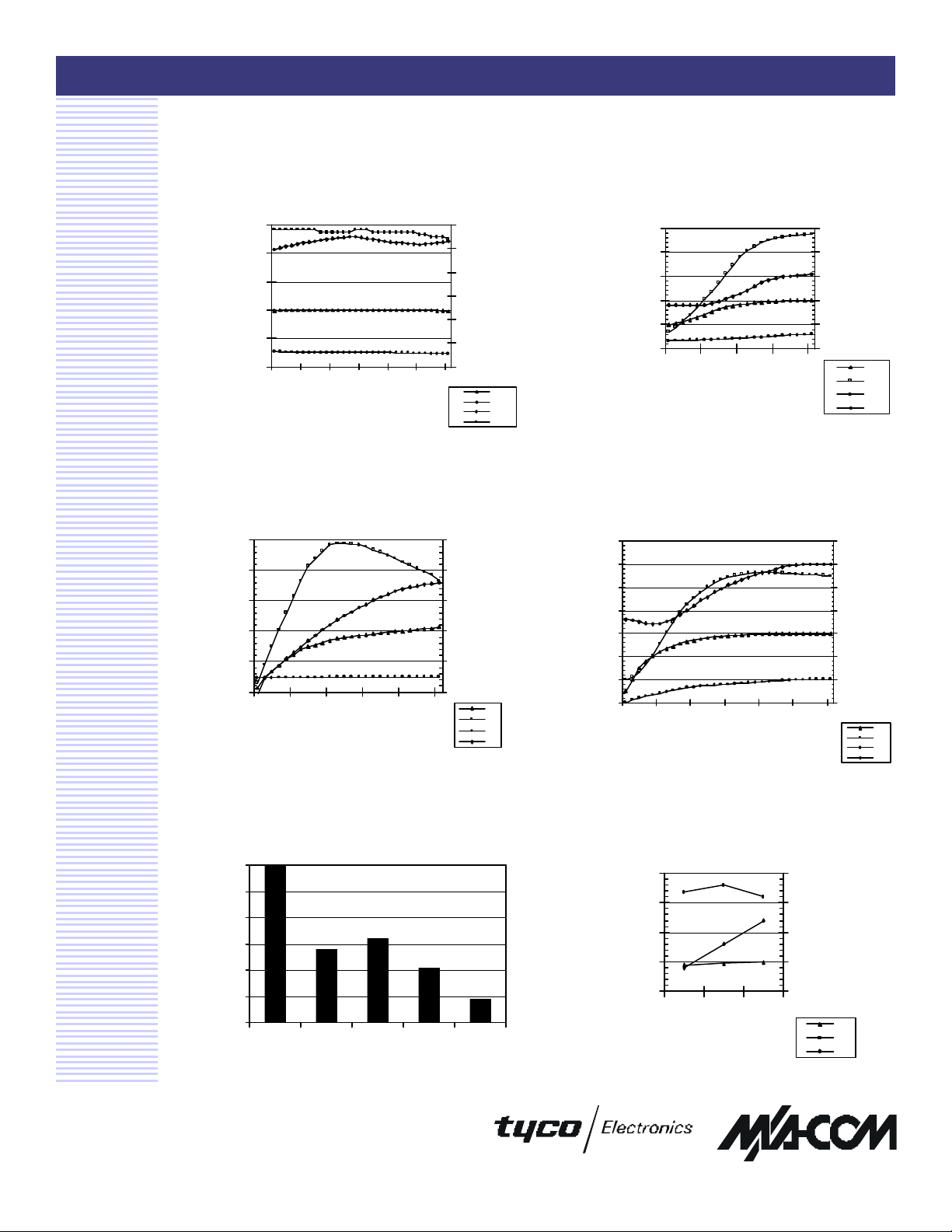
Typical Performance Curves
Output Power, Drain Currents, and Efficiency vs.
Frequency V
DD2
= 3 V , V
= 2.5 V, P
DD1
= 0 dBm
IN
MA02305AK
V 1.00
Output Power, Drain Currents and Efficiency vs.
Input Power V
= 3 V , ƒ = 2450 MHz, V
DD2
DD1
= 2.5V
50
40
30
65
55
45
35
20
10
Pout (dBm), PAE (%)
0
2300 2350 2400 2450 2500 2550 2600
Frequency (MHz)
25
15
5
Pout
PAE
Id1
Id2
Output Power, Drain Currents and Efficiency vs.
Supply Voltage
P
= 0 dBm , ƒ = 2450 MHz, V
IN
50
40
30
20
10
DD1
= 2.5 V
100
80
60
40
20
Pout (dBm), PAE (%)
0
0 1 2 3 4 5
VD2 (volts)
0
Pout
PAE
Id1
Id2
Id1, Id2 (mA)
Output Power, Drain Currents and Efficiency vs.
V
P
IN
Id1, Id2 (mA)
50
40
30
(%)
20
10
0
-15 -10 -5 0 5
Input Power (dBm)
for Power Control
DD1
= 0 dBm , ƒ = 2450 MHz, V
60
50
40
30
20
10
0
Pout (dBm), PAE (%)
-10
0.0 0.5 1.0 1.5 2.0 2.5 3.0
VD1 (volts)
DD2
= 3 V
100
80
60
40
20
0
70
60
50
40
30
20
10
0
Id1, Id2 (mA)
Pout
PAE
Id1
Id2
Id1, Id2 (mA)
Pout
PAE
Id1
Id2
Specifications subject to change without notice.
n North America: Tel. (800) 366-2266
n Asia/Pacific: Tel.+81-44-844 -8296, Fax +81-44-844-8298
n Europe: Tel. +44 (1344) 869 595, Fax+44 (1344) 300 020
Visit www.macom.com for additional data sheets and product information.
Harmonics
P
= 0 dBm , ƒ0 = 2450 MHz, V
IN
20
10
0
-10
-20
-30
-40
fo 2fo 3fo 4fo 5fo
= 2.5V, V
DD1
DD2
= 3V
Output Power, Input Return Loss and Efficiency
vs. Temperature
P
= 0 dBm , ƒ = 2450 MHz, V
IN
50
40
30
(%)
20
10
-40 25 80
Temperature (C)
= 2.5 V, V
DD1
= 3 V
DD2
-10
-15
-20
-25
-30
Input Return Loss (dB)
Pout
PAE
IRL
 Loading...