M A COM MA02303GJ-SMB, MA02303GJ-R7, MA02303GJ-R13 Datasheet

RF Power Amplifier IC
for 2.4 GHz ISM
MA02303GJ
Features
• Perfect for 802.11B, HOP, SWAP, HOMERF,
Bluetooth, WDECT, MDS, MMDS
• Single Positive Supply
• Power Added Efficiency As High As 55 Percent
• IP
= +43 dBm
3
• Output Power 26.5 dBm @ 3.3 V
• Output Power 28.5 dBm @ 5.0 V
• 100 Percent Duty Cycle
• 2200 to 2600 MHz Operation
• 8 Pin MSOP Full Downset Plastic Package
• Operates Over Wide Ranges of Supply Voltage
• Self-Aligned MSAG
®
-Lite MESFET Process
Description
The MA02303GJ is an RF power amplifier based on
M/A-COM’s Self-Aligned MSAG MESFET Process.
This product is designed for use in 2.4 GHz ISM
products. For booster applications, it features a low
power “bypass” mode and output power control
Ordering Information
Part Number Description
MA02303GJ-R7 7 inch, 1000 piece reel
MA02303GJ-R13 13 inch, 3000 piece reel
MA02303GJ-SMB Sample test board
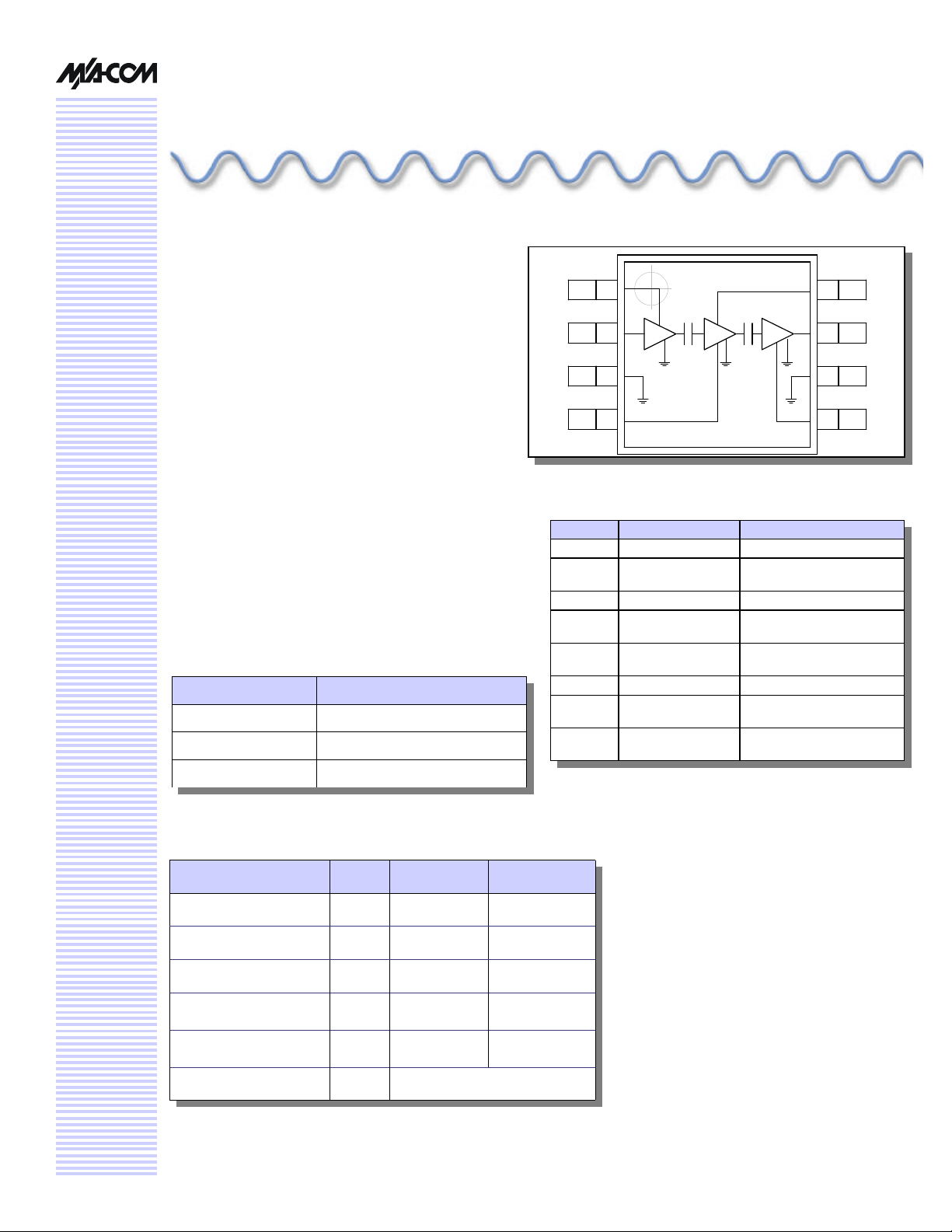
Functional Schematic
PIN 1
PIN Configuration
PIN Function Description
1
2
3 GND Ground
4
5
6 GND Ground
7
8
Package bottom is electrical and thermal ground
V
RF
V
V
RF
V
D1
G2
G3
D2
IN
OUT
/ V
/ V
G1
D3
Drain voltage, first stage
RF input and drain
voltage for first stage
Gate bias voltage,
second stage
Gate bias voltage,
third stage
RF output and drain
voltage for third stage
Drain voltage for
second stage
PIN 8
Absolute Maximum Ratings 1
Rating Symbol Value Unit
DC Supply Voltage
RF Input Power
Junction Temperature
Storage Temperature
Operating Temperature
Moisture Sensitivity
1. Beyond these limits, the device may be damaged or device reliability
reduced. Functional operation at absolute-maximum-rated conditions is
not implied.
VDD
P
IN
T
J
T
STG
T
OPER
JEDEC Level 1
5.5 V
10 mW
150 °C
-40 to +150 °C
-40 to +100 °C

RF Power Amplifier IC for 2.4 GHz ISM
MA02303GJ
Electrical Specifications: V
= +3.3 V, P
DD
= -2 dBm, Duty Cycle = 100 %,
IN
TS = 37 °C (Note 1), measured on evaluation board shown in Figure 11.
Characteristic Symbol Min. Typ. Max. Unit
Frequency Range
Output Power, ƒ = 2450 MHz
Power Added Efficiency, ƒ = 2450 MHz η
Current, ƒ = 2450 MHz
Current for linear operation, ƒ = 2450 MHz,
PIN adjusted for P
= 20.0 dBm +/- 0.2 dBm
OUT
Gain, ƒ = 2450 MHz,
PIN adjusted for P
= 20.0 dBm +/- 0.2 dBm
OUT
Harmonics, ƒ = 2450 MHz
Input VSWR, ƒ = 2450 MHz
Off Isolation (V
DD
=0 V)
Thermal Resistance, junction to package bottom
Third Order Intercept Point
Load Mismatch (V
Stability (P
IN
= 5.5 V, VSWR = 8:1, PIN = 0 dBm)
DD
= -2 to 2 dBm, VDD = 0-5.5 V, Load VSWR = 5:1,
all phases)
ƒ 2400 2500 MHz
P
OUT
I
DD
I
DD
G 29.5 dB
2ƒ, 3ƒ, 4 ƒ -40 dBc
— — 2.0:1 —
— 40 dB
R
TH
IP
3
—
—
25.3 26.5 — dBm
51 %
265 415 mA
415 mA
25
43 dBm
No Degradation in Power Output
All non-harmonically related outputs more
than 60 dB below desired signal
°C/W
1. TS is the temperature measured at the soldering point of the downset paddle on the bottom of the IC.
Specifications subject to change without notice.
n North America: Tel. (800) 366-2266
n Asia/Pacific: Tel.+81-44-844-8296, Fax +81-44-844-8298
n Europe: Tel. +44 (1344) 869 595, Fax+44 (1344) 300 020
Visit www.macom.com for additional data sheets and product information.
2

RF Power Amplifier IC for 2.4 GHz ISM
B
DD
B
DD
B
B
DD
B
DD
DD1
DD2
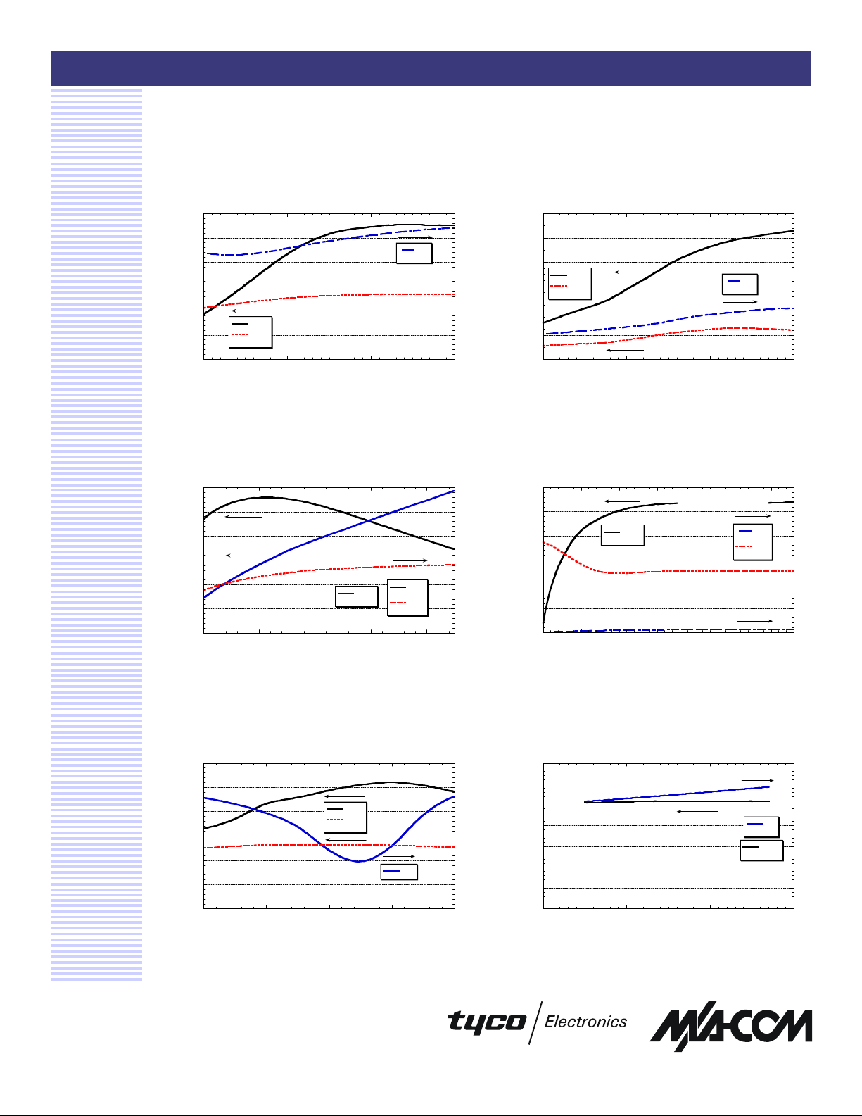
Typical Characteristics
(Measured data from process nominal devices)
MA02303GJ
Output Power, Drain Current and
Efficiency vs. Input Power
60
50
40
30
20
(dBm), PAE (%)
OUT
10
P
0
-10 -5 0 5
PAE
P
OUT
V
= 3.3 V
DD1, 2, 3
F = 2450 MHz
PIN (dBm)
Output Power, Drain Current and Efficiency
vs. Supply Voltage
60
50
40
30
20
(dBm), PAE (%)
OUT
10
P
0
PAE
P
OUT
PIN = -2 dBm
F = 2450 MHz
P
OUT
I
DD
1 2 3 4 5
PIN (dBm)
PAE
I
DD
Output Power, and Drain Current vs. Input
Power for Low Current “Bypass” Mode
(V
= 3.3 V, V
DD1,2
300
250
I
DD
200
150
100
50
0
(mA)
I
(dBm), PAE (%)
OUT
P
12
10
8
PAE
6
P
OUT
4
2
0
-10 -5 0 5
= 0.0 V)
DD3
V
= 3.3 V, V
DD1, 2
F = 2450 MHz
DD3
= 0.0 V
300
250
200
I
DD
150
100
(mA)
I
50
0
PIN (dBm)
Output Power, Drain Current and Efficiency
for Power Control
DD1
P
OUT
600
500
I
I
DD1
DD2
400
300
200
(mA)
, I
I
100
0
V
(V)
DD1
0.35
0.30
0.25
0.20
0.15
0.10
0.05
(A)
I
vs. V
30
25
20
15
(dBm)
OUT
10
P
5
0
0.0 0.5 1.0 1.5 2.0 2.5 3.0
Output Power, Input Return Loss and
Efficiency vs. Frequency
60
50
40
30
20
(dBm), PAE (%)
OUT
P
P
= - 2 dBm
IN
VDD = 3.3 V
10
0
2200 2300 2400 2500 2600
FREQUENCY (MHz)
Specifications subject to change without notice.
PAE
P
OUT
IRL
0
-5
-10
-15
-20
-25
-30
IRL (dB)
Output Power and Drain Current vs.
Temperature at VDD = +3.0 V
35
30
25
20
(dBm)
15
OUT
P
PIN = - 2 dBm
10
VDD - 3.0 V
5
F = 2450 MHz
0
-50 0 50 100
Temperature, TS (oC)
350
300
250
I
200
DD
P
OUT
150
(mA)
I
100
50
0
3
n North America: Tel. (800) 366-2266
n Asia/Pacific: Tel.+81-44-844-8296, Fax +81-44-844-8298
n Europe: Tel. +44 (1344) 869 595, Fax+44 (1344) 300 020
Visit www.macom.com for additional data sheets and product information.
 Loading...