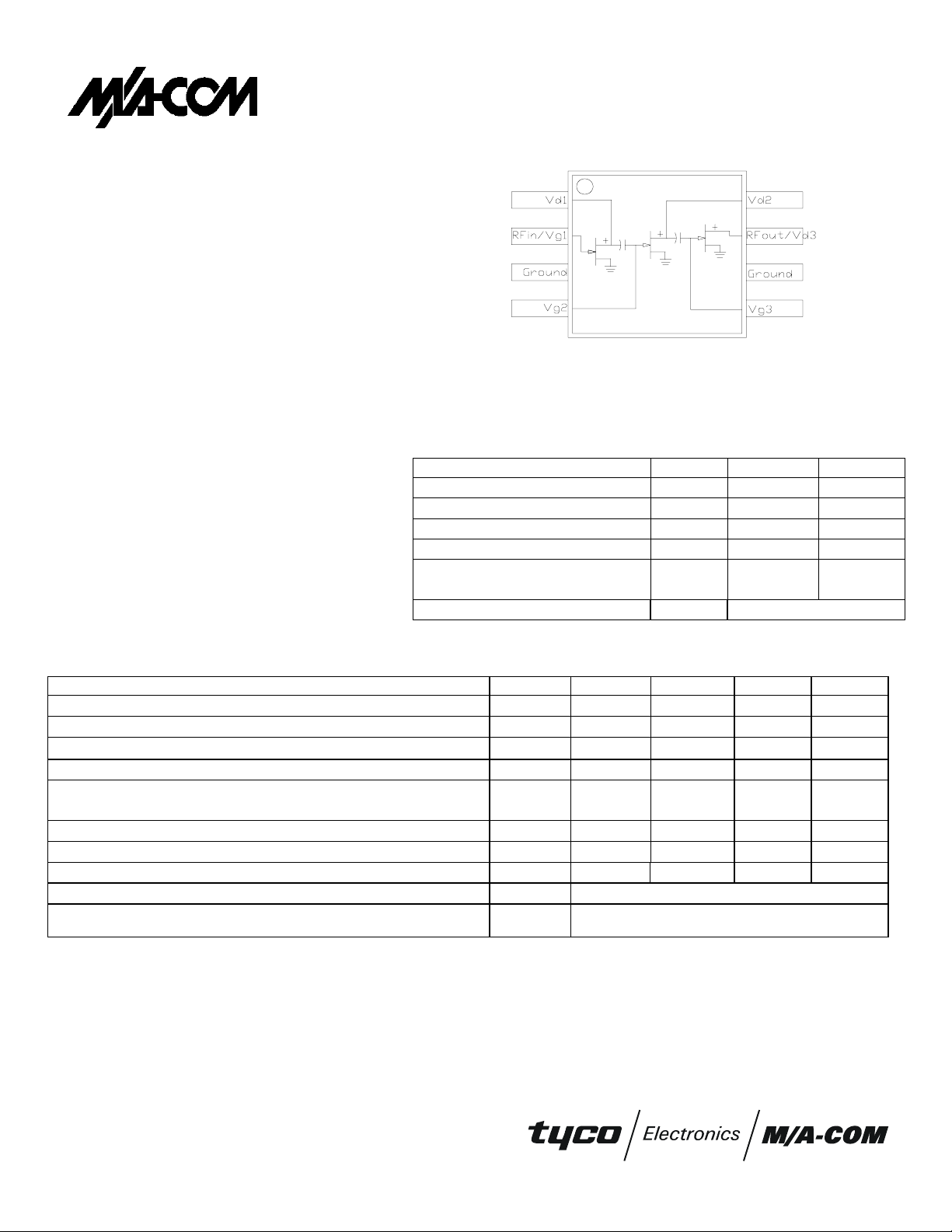
M A COM MA02206GJ Datasheet

MA02206GJ
3.6V 0.5W RF Power Amplifier IC
for DECT
FEATURES
•= Single Positive Supply
•= 57% Power Added Efficiency
•= Operation down to 1.2 V
•= 100% Duty Cycle
•= 1800 to 2000 MHz Operation
•= 8 Pin Full Downset MSOP Plastic Package
•= Accommodates Battery Charging Conditions up to
5.6 Volts
•= Self-Aligned MSAG
®
-Lite MESFET Process
8 Lead MSOP Package
Package bottom is electrical and thermal ground
DESCRIPTION MAXIMUM RATINGS (Beyond these limits, the device may be damaged or device
reliability reduced. Functi onal operation at absolute–maximum–rated conditions is not implied.)
The MA02206GJ is a DECT Power amplifier
based on M/A-COM’s Self-Aligned MSAG
MESFET Process. This product is designed
for use in 3.6 V DECT handsets and base
stations.
Rating Symbol Value Unit
DC Supply Voltage VDD 6.0 V
RF Input Power PIN 10 mW
Junction Temperature TJ 150 °C
Storage Temperature Range T
Operating Temperature
T
STG
OPER
-40 to +150
-40 to +100
Range
Moisture Sensitivity
JEDEC Level 1
ELECTRICAL CHARACTERISTICS V
board shown in Figure 9.
Characteristic Symbol Min Typ Max Unit
= +3.6 V, PIN= -2 dBm, Duty Cycle = 100 %, TS = 37 °C (Note 1), measured on evaluation
DD
Frequency Range ƒ 1880 1900 1930 MHz
Output Power (1900 MHz)
Power Added Efficiency (1900 MHz)
Drain Current (1900MHz)
Harmonics
P
25.9 26.9 27.9 dBm
OUT
η
52 57 %
IDD 228 330 mA
2ƒo
3ƒ
-37
o
-38
-30
-34
Input VSW R — 1.3:1 2.0:1 —
Off Isolat ion (V
Thermal Resistance, Junct i on to soldering point (T
Load Mismatch (V
Stability (P
Note 1: T
Note 2: Output power and efficiency have been optimized for input drive levels between –2 to +2 dBm. Stability is only specified within this range. For
is the temperature m easured at the soldering point of the downset paddl e on the bottom of the IC.
s
operation outside of this range, contact the fact ory.
=0 V) — 38 44 dB
DD
= 4.5 V, VSW R = 5: 1, P
DD
= -2 to 2 dBm, V
IN
) (Note 1) —
s
= -2 dBm) —
IN
= 0-5.0 V, Load VSWR = 5:1, all phases) —
DD
No Degradation in Power Output
All non-harmonically related outputs more than
25
60 dB below desired signal
°C
°C
dBc
°C/W
Specifications subject to change without notice.
North America: Tel. (800)366-2266, Fax (800)618-8883
Asia/Pacific: Tel. +81-44-844-8296, Fax +81-44-844-8298
Europe: Tel. +44 (1344) 869 595, Fax +44 (1344) 300 020
Visit www.macom.com for additional data sheets and product information
902407 E

3.6V 0.5W RF Power Amplifier IC for DECT MA02206GJ
TYPICAL CHARACTERISTICS (Measured data from process nomi nal devi ces)
6
5
OUT
- P
4
DD3
* V
3
DD3
2
(W) = I
DISS
P
1
0
-50 0 50 100 150
Temperature, T
(°C)
S
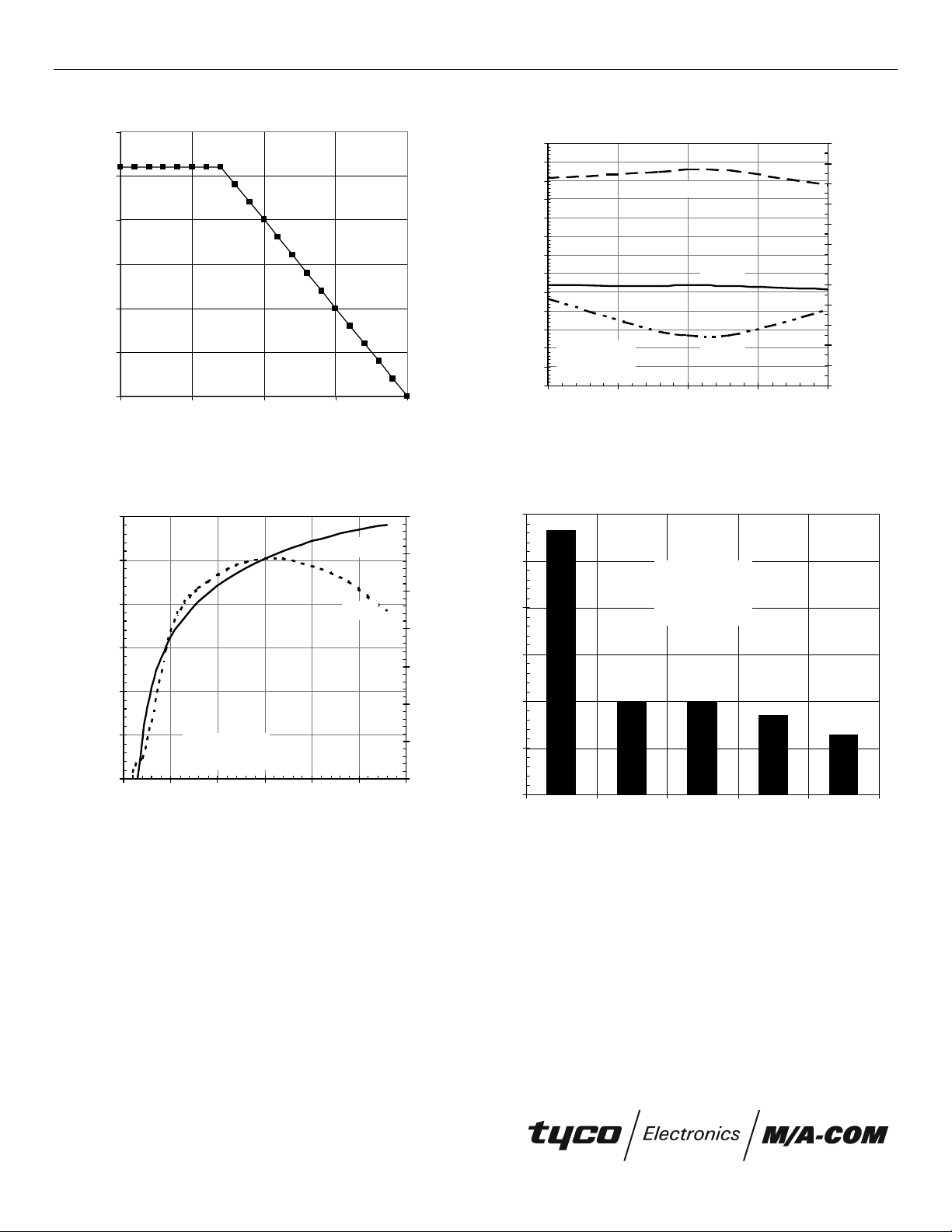
Figure 1. Maximum operating temperature (TS) to
maintain <150°C junction temperature.
65
60
55
50
45
40
35
30
25
20
15
Pout (dBm) and PAE (%)
10
VDD = 3.6 V
5
P
= -2 dBm
IN
0
1800 1850 1900 1950 2000
PAE
P
OUT
VSWR
Frequency (MHz)
6.0
5.5
5.0
4.5
4.0
3.5
3.0
2.5
2.0
1.5
1.0
0.5
0.0
VSWR
Figure 2. Output power, power added efficiency, and
input VSWR vs. frequency
30
25
P
OUT
70
60
50
20
PAE
40
15
(dBm)
OUT
P
30
PAE (%)
10
20
5
PIN = -2 dBm
10
f = 1900 MHz
0
0
0123456
Supply Voltage (Volts)
Figure 3. Output power and power added efficiency vs.
supply voltage
30
20
10
-10
-20
-30
VDD = 3.6 V
P
= -2 dBm
IN
f
= 1900 MHz
o
0
ƒο 2ƒο 3ƒο 4ƒο 5ƒο
Figure 4. Harmonics
Specifications subject to change without notice.
North America: Tel. (800)366-2266, Fax (800)618-8883
Asia/Pacific: Tel. +81-44-844-8296, Fax +81-44-844-8298
Europe: Tel. +44 (1344) 869 595, Fax +44 (1344) 300 020
Visit www.macom.com for additional data sheets and product information
902407 E
 Loading...