M A COM MA02205AF Datasheet

MA02205AF
3.6V 0.5W RF Power Amplifier IC
for DECT
Applications
DECT
PCS
Personal Wireless Telephony (PWT)
Cordless PBX
Radio/Wireless Local Loop (RLL/WLL)
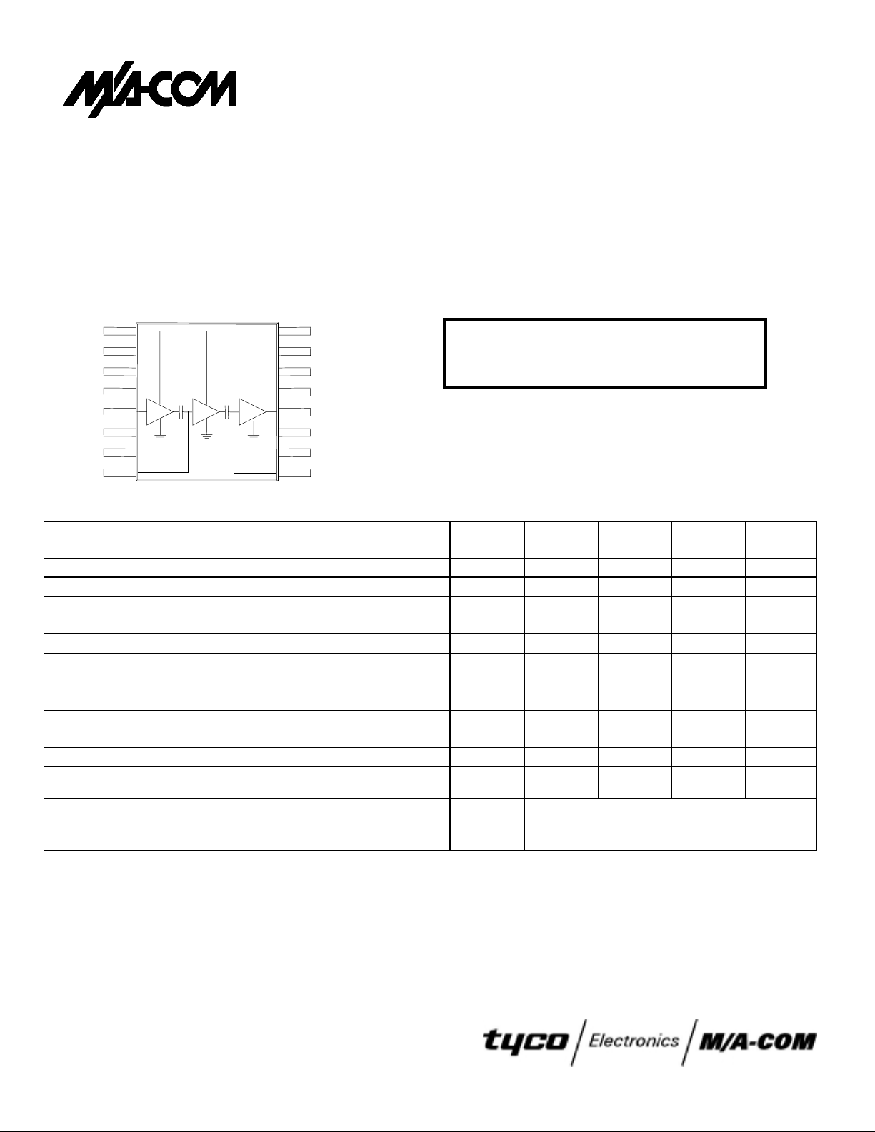
V
DD1
N/C
GND
GND
RFIN/V
GG1
GND
GND
V
GG2
ELECTRICAL CHARACTERISTICS V
Characteristic Symbol Min Typ Max Unit
Frequency Range ƒ 1880 1930 MHz
Output Power, f = 1900 MHz P
Power Gain GP 29.3 dB
Gain Slope, f=1930 to 1880 MHz — 0.008 0.012 dB/MH
Power Added Efficiency, f = 1900 MHz
Drain Current IDD 270 mA
Harmonics 2ƒ
Input VSW R (V
(V
Off Isolat ion (V
Thermal Resistance (Junction of 3
13)
Load Mismatch (V
Stability (P
Load VSWR = 5:1)
= -2 dBm, VDD = 0-5.5 V, TS= -40 to +85 °C,
IN
= 0.0 V)
DD
= 3.6 V)
DD
=0 V) — 40 dB
DD
= 5.5 V, VSW R = 8: 1, P
DD
rd
stage FET to solder point of pin
V
DD2
GND
GND
GND
RF
OUT/VDD3
GND
GND
V
GG3
= -2 dBm) —
IN
= 3.6 V, PIN= -2 dBm, TA=25 °C, Output externally matched to 50 Ω
DD
Features
•= Single Positive Supply
•= 54% Power Added Efficiency
•= 100% Duty Cycle
•= 1.2:1 Input VSWR in both On and Off states
•= 1800 to 2000 MHz Operation
•= 16 Pin TSSOP Plastic Package
•= Accommodates Battery Charging Conditions up to 5.5 Volts
•= Self-Aligned MSAG
®
-Lite MESFET Process
54% PAE
100% Duty Cycle
26.2 27.2 28.2 dBm
OUT
z
η
o
3ƒo
—
—
51 °C/W
R
TH J-S
—
49 54 %
-34
-38
1.2:1
1.2:1
No Degradation in Power Output
All non-harmonically related outputs more than
60 dB below desired signal
-30
-34
2.0:1
2.0:1
dBc
dBc
—
—
Specifications subject to change without notice.
North America: Tel. (800)366-2266, Fax (800)618-8883
Asia/Pacific: Tel. +81-44-844-8296, Fax +81-44-844-8298
Europe: Tel. +44 (1344) 869 595, Fax +44 (1344) 300 020
Visit www.macom.com for additional data sheets and product information
901981 E

3.6V 0.5W RF Power Amplifier IC for DECT MA02205AF
MAXIMUM RATINGS (T
Rating Symbol Value Unit
DC Supply Voltage (Pins 1, 12, 16) V
RF Input Power PIN 3 mW
Junction Temperature TJ 150 °C
Storage Temperature Range T
APP LICATION INFORMATION
+V
DD
= 25 °C unless otherwise noted)
A
5.5 Vdc
DD
-40 to +150 °C
STG
T4
C4
L3
RF
T5
C6
C5
9
RF
1
C1 C2
IN
C3
T1
R1
T2
L1
T3
L2
N/C
2
3
4
5
6
7
8
16
15
14
13
12
11
10
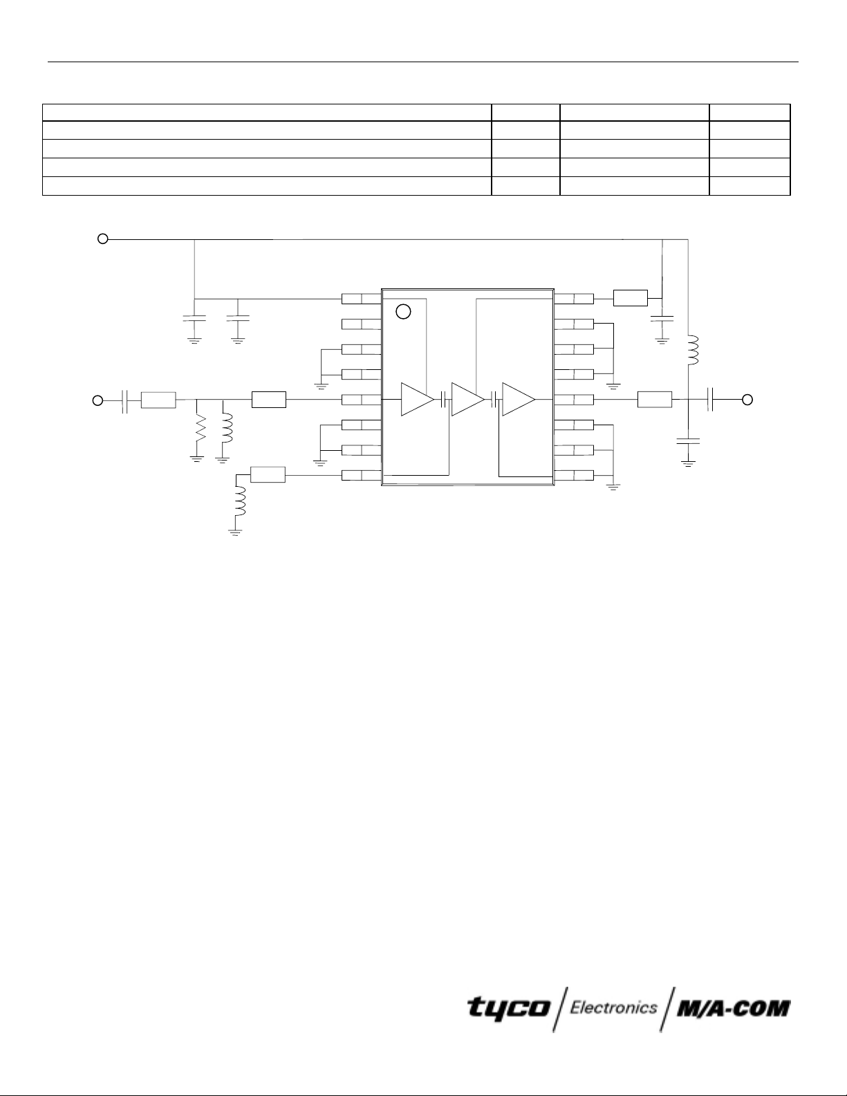
Figure 1. Evaluation Board Schematic
List of components:
C1 = 100 pF DLI multilayer ceramic chip capacitor (C11AH101K5TX L)
C2 = 10 pF DLI multilayer ceramic chip capacitor (C11AH1R0B5TX L)
C3 = 0.7 pF DLI multilayer ceramic chip capacitor (C11AH0R7B5T XL)
C4 = 10 pF DLI multilayer ceramic chip capacitor (C11AH1R0B5TX L)
C5 = 2.2 pF DLI multilayer ceramic chip capacitor (C11AH2R2B5T XL)
C6 = 100 pF DLI multilayer ceramic chip capacitor (C11AH101K5TX L ) ( DC blocking capacitor)
L1 = 2.7 nH Toko chip inductor (T KS2362CTND)
L2 = 3.3 nH Toko chip inductor (T KS2363CTND)
L3 = 27 nH Coilcraft chip inductor (1008CS.270XMBB)
R1 = 300 Ω chip resistor
T1 = 0.19" of 50 Ω==g r ounded coplanar waveguide (60 m il GETEK board)
T2 = 0.12" of 50 Ω==g r ounded coplanar waveguide (60 m il GETEK board)
T3 = 0.39" of 75 Ω==g r ounded coplanar waveguide (60 m il GETEK board)
T4 = 0.11" of 75 Ω==g r ounded coplanar waveguide (60 m il GETEK board)
T5 = 0.14" of 50 Ω==g r ounded coplanar waveguide (60 m il GETEK board)
Component layout and printed circuit board drawing for RF IC evaluation board are shown in Figure 9.
OUT
Specifications subject to change without notice.
North America: Tel. (800)366-2266, Fax (800)618-8883
Asia/Pacific: Tel. +81-44-844-8296, Fax +81-44-844-8298
Europe: Tel. +44 (1344) 869 595, Fax +44 (1344) 300 020
Visit www.macom.com for additional data sheets and product information
901981 E
 Loading...