M A COM MA02204AF Datasheet

MA02204AF
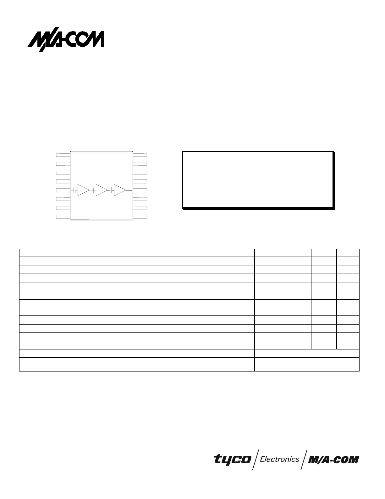
3.3V 0.5W RF Power Amplifier IC
for DECT
Applications
DECT
PCS
Personal Wireless Telephony (PWT)
Cordless PBX
Radio/Wireless Local Loop (RLL/WLL)
V
DD1
N/C
GND
GND
RF
IN
GND
GND
N/C
V
DD2
GND
GND
GND
RF
GND
GND
N/C
OUT/VDD3
Features
•= Single Positive Supply
•= 16 Pin TSSOP Plastic Package
•= Class AB Bias
•= 1700 to 2200 MHz Operation
•= 50 Ω Input Impedance
•= Simple Output Match
•= Accommodates Battery Charging Conditions up to 5 Volts
•= Self-Aligned MSAG
®
-Lite MESFET Process
•= Guaranteed Stability and Ruggedness
Typical 3.3 Volt Performance
27 dBm Output Power
32 dB Power Gain
42% Power Added Efficiency
-40 dBc 2nd Harmonic
-45 dBc 3
rd
Harmonic
ELECTRICAL CHARACTERISTICS V
Characteristic Symbol Min Typ Max Unit
Frequency Range ƒ 1880 1905 1930 MHz
Output Power P
Power Gain GP 31 32 33 dB
Power Added Efficiency
Drain Current IDD — 360 470 mA
Harmonics 2ƒ
Input VSW R — — 1.3:1 2.0:1 —
Off Isolat ion (V
Thermal Resistance (Junction of 3
Load Mismatch (V
Stability (P
Note 1: Ts is the temperature m easured at the soldering point of pin 13, mounted on 60 mil GETEK evaluation board in a free air condition with
ambient room temperature T
room temperature conditions , operating at 500 mW of load power (V
=0 V) — 35 40 — dB
DD
= 5 V, VSWR = 6:1, P
DD
= -6 to +5 dBm, VDD = 0-5 V, T
IN
rd
stage FET to solder point of pin 13) R
IN
= -40 to +85 °C, Load VSW R = 6: 1) —
S
=25°C. The electrical data pres ented herein was taken with the evaluation board shown in Figures 1 & 6, under
A
= 3.3 V, PIN= -5 dBm, TS=55 °C (Note 1), Output externally matc hed to 50 Ω
DD
26 27 28 dB
OUT
η
o
3ƒo
TH J-S
= +5 dBm) —
= 3.3 V), unless otherwise spec i fied.
DD
38 42 — %
—
—
-40
-45
— — 60 °C/
No Degradation in Power Output
All non-harmonically related outputs
more than 60 dB below desired signal
-34
-38
dBc
dBc
W
Specifications subject to change without notice.
North America: Tel. (800)366-2266, Fax (800)618-8883
Asia/Pacific: Tel. +81-44-844-8296, Fax +81-44-844-8298
Europe: Tel. +44 (1344) 869 595, Fax +44 (1344) 300 020
Visit www.macom.com for additional data sheets and product information
901642 K

3.3V 0.5W RF Power Amplifier IC for DECT MA02204AF
V
MAXIMUM RATINGS (T
Rating Symbol Value Unit
DC Supply Voltage (Pins 1, 12, 16) V
RF Input Power PIN 3 mW
Junction Temperature TJ 150 °C
Storage Temperature Range T
APPLICATION INFORMATION
+
DD (+3.3V)
= 25 °C unless otherwise noted)
A
C1 C2
5 Vdc
DD
-40 to +150 °C
STG
INPU T
RF
1
2
N/C
3
4
5
6
7
8
N/C N/C
16
15
14
13
12
T1
11
10
9
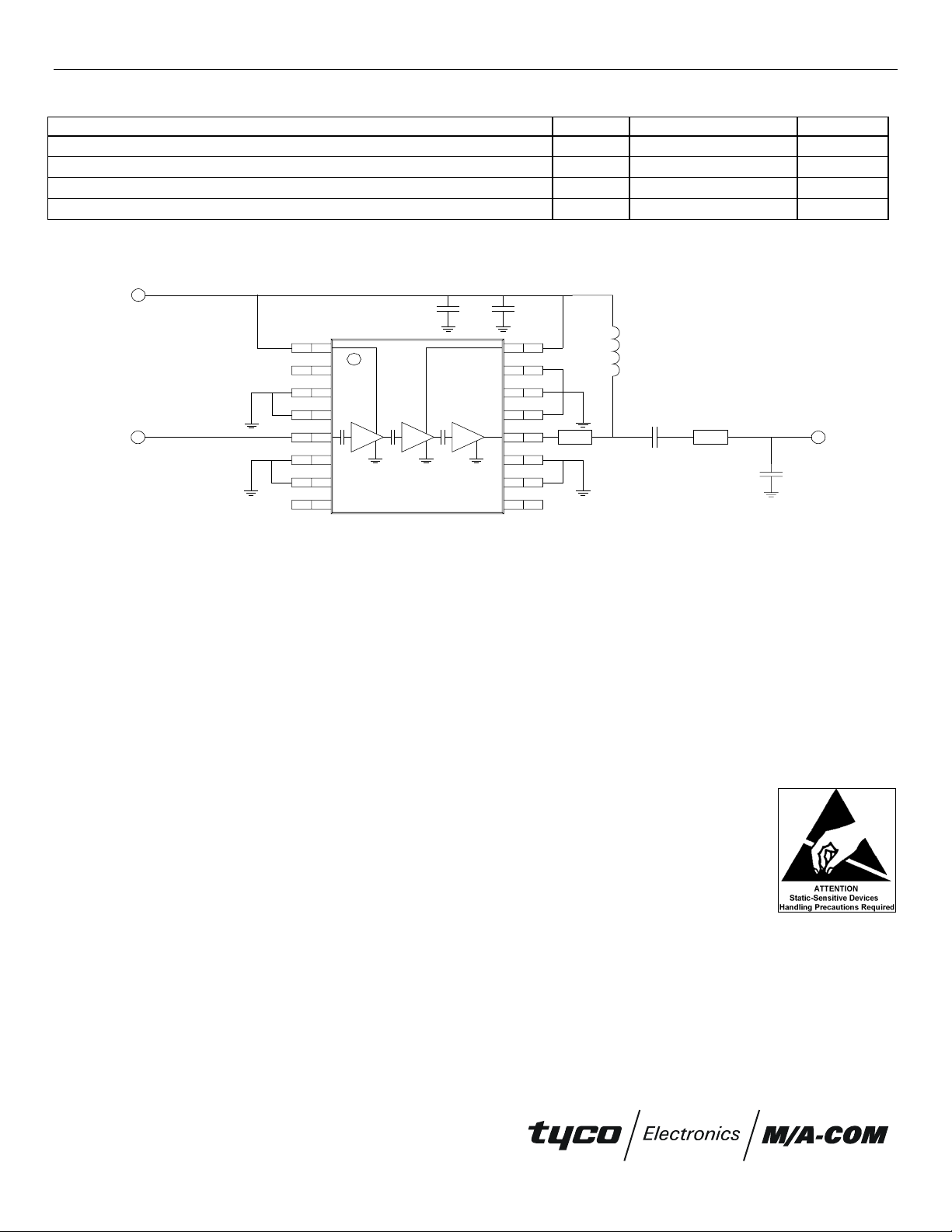
Figure 1. Evaluation Board Schematic
List of components:
C1 = 0.1µF Kemet multilayer ceramic chip capacitor (C1206C104K5RAC)
C2 = 4700 pF Kemet multilayer ceramic chip capacitor (C0805C472K5RAC)
C3 = 6.2 pF DLI multilayer ceramic chip capacitor (C11AH6R2B5TXL)
C4 = 2 pF DLI multilayer ceramic chip capacitor (C11AH2R0B5TXL)
L1 = 39 nH Coilcraft chip inductor (1008CS.390XMBB)
T1 = 0.10" of 50
T2 = 0.07" of 50
Ω==grounded coplanar waveguide (60 mil GETEK board)
Ω==grounded coplanar waveguide (60 mil GETEK board)
L1
C3
T2
OUTPUT
RF
C4
Component layout and printed circuit board drawing for RF IC evaluation board are shown in Figure 6.
Specifications subject to change without notice.
North America: Tel. (800)366-2266, Fax (800)618-8883
Asia/Pacific: Tel. +81-44-844-8296, Fax +81-44-844-8298
Europe: Tel. +44 (1344) 869 595, Fax +44 (1344) 300 020
Visit www.macom.com for additional data sheets and product information
901642 K
 Loading...