

3.4 V, 1.2 W RF Power Amplifier IC
V 1.0
DD1
MA02107AF
Features
§ Ideal for Pager Applications
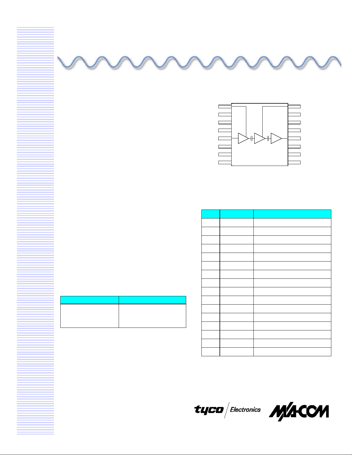
Functional Schematic
§ +30.8 dBm Output Power
DD2
§ 30.8 dB Power Gain
§ Single Positive Supply
§ Class AB Bias
§ 50 Ohm Input Impedance
§ Single Capacitor Output Match
Description
The MA02107AF is a three stage power amplifier,
V
N/C
GND
GND
RF IN
GND
GND
N/C
designed for paging applications to have an output
power of +30.8 dBm with an input power of 0 dBm.
This power amplifier operates at +3.4 volts with
55% typical power added efficiency. The
MA02107AF is mounted in a standard outline 16-pin
TSSOP plastic package.
The MA02107AF is fabricated using M/A-COM’s
self-aligned MSAG®-Lite MESFET process for a low
single supply voltage, high power efficiency, and
excellent reliability.
Ordering Information
Part Number Description
MA02107AF-R7 7 inch, 1000 piece reel
MA02107AF-R13
MA02107AF-SMB
13 inch, 3000 piece reel
Sample Test Board
Pin Configuration
Pin Function Description
1 V
2 N/C Not Connected
3 GND Ground
4 GND Ground
5 RFIN RF Input
6 GND Ground
7 GND Ground
8 N/C Not Connected
9 N/C Not Connected
10 GND Ground
11 GND Ground
12 RF
13 GND Ground
14 GND Ground
15 GND Ground
16 V
First Stage Supply Voltage
DD1
OUT/VDD3
RF Output/Third Stage Supply
Second Stage Supply Voltage
DD2
V
GND
GND
GND
RF OUT/VDD3
GND
GND
N/C
Specifications subject to change without notice.
n North America: Tel. (800) 366-2266
n Asia/Pacific: Tel.+81-44-844-8296, Fax +81-44-844-8298
n Europe: Tel. +44 (1344) 869 595, Fax+44 (1344) 300 020 1
Visit www.macom.com for additional data sheets and product information.
Part Description
V 1.0
< +85ºC, RBW
3.4 V, 1.2 W RF Power Amplifier IC MA02107AF
Electrical Specifications: TS = 35 °C1, Z0 = 50 Ω Ω
Parameter Test Conditions Units Min Typ Max
Frequency MHz 900 942
Output Power dBm 30.0 30.8
Power Gain dB 30.8
Power Added Efficiency % 45 55
Input Return Loss dB 10 15
2nd Harmonics dBc -35 -29
3rd Harmonics dBc -50 -45
Thermal Resistance 3rd Stage FET to solder point of pin 13
+3.0 V < V
Stability
1. Ts is the temperature measured at the soldering point of pin 13.
2. Unless otherwise specified, input power is 0 dBm, VDD is +3.45 V, and test frequency is 900 MHz.
3. The output is externally matched to 50 ohms.
VSWR < 5:1, -40ºC < T
= 3 MHz max hold
< +5.0 V, P
CC
< +31 dBm,
OUT
C
2,3
o
C/W 41
All spurs < -60 dBc
Absolute Maximum Ratings1
Parameter Absolute Maximum
Max Input Power +6 dBm
Operating Voltages +5.0 volts
Operating Temperature, Ts
Channel Temperature +150 °C
Storage Temperature -40 °C to +150 °C
1. Exceeding any one or combination of these limits may cause permanent damage.
-40 °C to +70 °C
Application Information
Static Sensitivity
Gallium arsenide integrated circuits are ESD sensitive and can be damaged by static electricity. Use proper ESD precautions when
handling these devices.
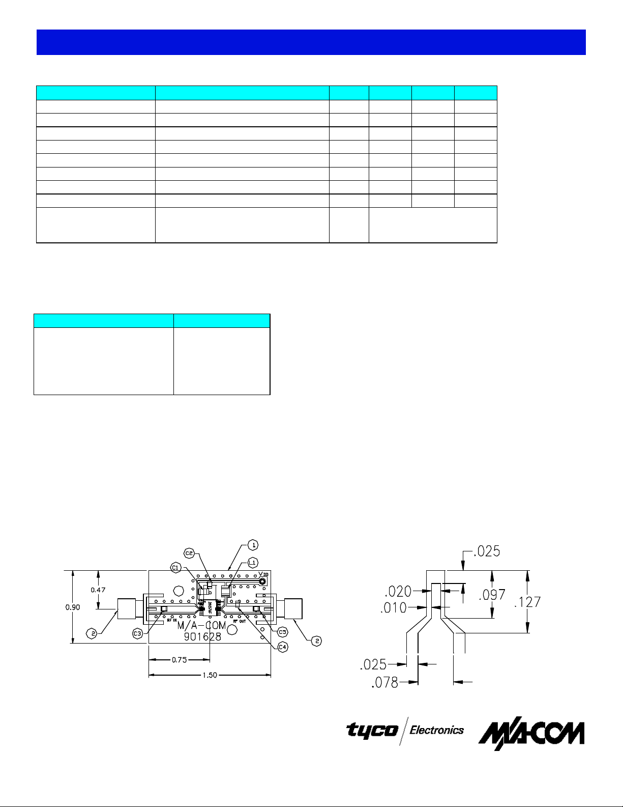
Board Layout
Sample Test Board 50 Ohm Lead Transition
Specifications subject to change without notice.
n North America: Tel. (800) 366-2266
n Asia/Pacific: Tel.+81-44-844-8296, Fax +81-44-844-8298
n Europe: Tel. +44 (1344) 869 595, Fax+44 (1344) 300 020 2
Visit www.macom.com for additional data sheets and product information.

Part Description
V 1.0
η
VSWR
3.4 V, 1.2 W RF Power Amplifier IC MA02107AF
Output Match Impedance (as seen from pin 12)
170
0.2
0
0.5
1
180
900 MHz
8.4 - j9.2
ΩΩ
-170
-160
925 MHz
850 MHz
-150
-140
-130
-120
-110
-100
-90
-80
Typical Performance Curves
Output Power and PAE vs. Input Power
40
35
60
50
Output Power, PAE, and VSWR vs. Fequency
60
50
η
3:1
30
25
20
, Output Power (dBm)
OUT
P
15
10
-10 -5 0 5
P
OUT
PIN, Input Power (dBm)
ƒ = 901 MHz
VDD = 3.4 V
Output Power and PAE vs. Supply Voltage
35
30
25
20
15
, Output Power (dBm)
10
OUT
P
5
η
POUT
ƒ
= 901 MHz
PIN = 0 dBm
40
30
20
Pwr Added Efficiency
10
0
70
60
50
40
30
20
η, Pwr Added Efficiency (%)
10
40
30
(dBm) and (%)
20
OUT
P
10
0
800 850 900 950 1000
ƒ, Frequency (MHz )
P
OUT
Harmonics
40
30
20
10
0
-10
, Output Power (dBm)
OUT
-20
P
-30
ƒο = 901 MHz
PIN = 0 dBm
VDD = 3.4 V
2:1
1:1
0
0.0 0.5 1.0 1.5 2.0 2.5 3.0 3.5 4.0
VDD, Supply Voltage (Volts)
0
-40
ƒο 2ƒο 3ƒο 4ƒο 5ƒο
Frequency
Specifications subject to change without notice.
n North America: Tel. (800) 366-2266
n Asia/Pacific: Tel.+81-44-844-8296, Fax +81-44-844-8298
n Europe: Tel. +44 (1344) 869 595, Fax+44 (1344) 300 020 3
Visit www.macom.com for additional data sheets and product information.

Part Description
V 1.0
RF
INPUT
+
VDD(+3.4V)
RF
OUTPUT
T1
12345
678910
1112131415
16
3.4 V, 1.2 W RF Power Amplifier IC MA02107AF
Application Schematic
C1 C2
L1
N/C
C3
N/C N/C
List of components:
C1 = 0.1µF Kemet multilayer ceramic chip capacitor (C1206C104K5RAC)
C2 = 4700 pF Kemet multilayer ceramic chip capacitor (C0805C472K5RAC)
C4 = 6.8 pF DLI multilayer ceramic chip capacitor (C11AH7R5B5TXL)
C3 = C5 = 100 pF DLI multilayer ceramic chip capacitor (DC Block; C11AH101K5TXL)
L1 = 39 nH Coilcraft chip inductor (1008CS.390XMBB)
T1 = 0.19" of 50 ohm grounded coplanar waveguide (60 mil GETEK board)
TSSOP-16 Package
Dimensions in
millimeters
SYMBOL MIN NOM MAX MIN NOM MAX
A 1.05 1.10 1.20 0.041 0.043 0.047
A1 0.05 0.10 0.15 0.002 0.004 0.006
A2 — 1.00 1.05 — 0.039 0.041
b 0.20 0.25 0.28 0.008 0.010 0.011
C — 0.127 — — 0.005 —
D 4.90 5.075 5.10 0.193 0.200 0.201
E 6.20 6.40 6.60 0.244 0.252 0.260
E1 4.30 4.40 4.50 0.169 0.173 0.177
e — 0.65 — — 0.025 —
L 0.50 0.60 0.70 0.020 0.024 0.028
L1 0.90 1.00 1.10 0.035 0.039 0.043
y — — 0.10 — — 0.004
θ
0° 4° 8° 0° 4° 8°
Dimensions in inches
C5
C4
NOTES:
1. Controlling dimension: mm
2. Lead frame material: EFTEC 64
3. Dimension “D” does not include mold flash, protrusions or gate burrs
4. Dimension “E” does not include interlead flash or protrusions
5. Tolerance: ±0.254 mm (±0.010″) unless otherwise specified
6. End flash max: 0.12 mm (0.005 ″)
Specifications subject to change without notice.
n North America: Tel. (800) 366-2266
n Asia/Pacific: Tel.+81-44-844-8296, Fax +81-44-844-8298
n Europe: Tel. +44 (1344) 869 595, Fax+44 (1344) 300 020 4
 Loading...